proof of concept implementation with the spartan 3e …jharris/research/super_project/... · proof...
TRANSCRIPT

Proof of Concept Implementation With the
SPARTAN 3E FPGA Evaluation Board for the
CAL POLY SuPER Project
By
Tony Wonsyld
Senior Project
ELECTRICAL ENGINEERING DEPARTMENT
California Polytechnic State University
San Luis Obispo
2008

2
TABLE OF CONTENTS
Section Page
Acknowledgments………………………..………………………4
I. Introduction…………………………………………………...5
II. Background……………………………………………………7
III. Requirements………………………………………………….9
IV. Hardware Design and Configuration ………………………..11
A. PWM Signal and Timer/Counter………………………………..11
B. Sensor ADC and Pre-Amp……………………………………...13
C. MUX Layout and Control……………………………………....14
D. Data Logging and Memory Control…………………………….17
E. Load Switch Control and LED Verification…………………....20
F. LCD User Display……………………………………………....21
V. Software Integration………………………………………………23
VI. Testing and Verification………………………………………….25
A. ADC and MUX………………………………………………….25
B. Memory…………………………………………………………26
C. PWM Output..…………………………………………………..27
D. Overall Timing………………………………………………….28
VII. Recommendations……………………………………………….31
VIII. Conclusions………………………………………………………33
Appendices
A: Bibliography……………………………………………………………32
B: UCF File………………………………………………………………..33
C: C Software File and Headers…………………………………………...35
1. Main.c…………………………………………………………….35
2. Lcd.c and Lcd.h…………………………………………………..39
3. Inputs.c and Inputs.h……………………………………………
4. Output.h…………………………………………………………..
5. IntC.c and IntC.h……………………………………………………
6. Spi.c and Spi.h…………………………………………………….
D: Senior Project Analysis……………………………………………….

3
List of Figures
Figures Page
Figure 2.1: Current Phase 1 Block Diagram………………………………………..6
Figure 2.2: Projected Block Diagram Using A Spartan 3E FPGA………………..8
Figure 3.1: Spartan 3E FPGA Development Kit…………………………………..10
Figure 4.1: Analog-to-Digital Converter Interface………………………………..13
Figure 4.2: Detailed View of Analog Capture Circuit……………………………..14
Figure 4.3: Functional Diagram and Truth Table For The LF 13508 MUX……16
Figure 4.4: DDR Controller Clocking Option For Asynchronous System………18
Figure 4.5: Functional Block Diagram For On-Board DDR SDRAM…………..19
Figure 4.6: Character Display Address Map For The LCD……………………...21
Figure 4.7: Sectioned LCD Screen Design…………………………………………22
Figure 5.1: Software Flow Diagram………………………………………………...24
Figure 6.2: Excerpt From main.c Program for Memory Test……………………26
Figure 6.3: PWM Output……………………………………………………………27
List of Table
Figures Page
Table 4.1: Programmable Gain Settings For The Pre-Amp………………….…..15
Table 6.1: A/D Conversion Accuracy………………………………………………25
Table 6.2: Elapsed Time for a Single Poll…………………………………………29
Table 6.2: Lower Time Bound of System …………………………………………30

4
Acknowledgments
I would like to thank Dr. Harris for bringing me on-board and letting me be
involved in this wonderful program. I cannot tell you how much I‟ve learned. Also, my
family who have all been so supportive, especially my mother and father, who I have
everything to thank because of them. I love you so much. Lastly, I would like to thank
Tom Hickock, for all of your help and wisdom. Your knowledge is priceless.

5
I. Introduction
In 2005, Dr. James Harris presented his white paper discussing a proposed
activity to develop a low-cost, sustainable source of solar power with a 20 year life
cycle[1]. The project is intended to help financially troubled regions with high levels of
solar radiation. In an ever-growing weak global economy, where government aid and
humanitarian projects lack funding, a possible solution has been brought to research by
the members of Cal Poly‟s Sustainable Power for Electronic Resources (SuPER).
With solar technology and energy conversion efficiency increasing every year,
Dr. Harris, along with Dr. Ali Shaban and various EE and CPE students have started a
prototype that aims to solve the fundamental problem of power distribution and
affordability. The idea is to harness solar energy via a solar panel to bring energy to
household necessities such as lighting and refrigeration for a cost of under $500.
Currently the project is still in Phase 1 and the estimated price tag is about $1500, but
great strides and improvements have been made along the way.
This project will help move into Phase 2 by producing a proof of concept that will
dramatically reduce overhead by replacing the current laptop with an FPGA device. The
lab top acts as the central device that stabilizes the entire system and processes all the
data and controlling algorithms. Technology has brought the FPGA industry into the
high performance market of computers, yet can be reprogrammed rapidly to adapt to
changing circumstances and environments. For greater control and reliability, progress is
currently underway to install an OS onto the FPGA [12]. This project focuses on the
actual interface functions for the FPGA to handle.

6
II. Background
The system is currently controlled by a laptop computer. The laptop is the
interface between data acquisition, the PIC microcontroller, the DC-DC converter, and
the MOSFET switches, shown in Figure 2.1. It is an integral component to the
functionality of the SuPER design, but consumes a large portion of power and is also
very costly.
Figure 2.1: Current Phase 1 Block Diagram [7]
7
In order to make the design more economically feasible, an FPGA is proposed to
substitute for the laptop. An FPGA offers a powerful alternative in terms of accessibility,
cost, and speed. The Spartan 3E development board is capable of performing all the
necessary control and acquisition requirements at a fraction of the cost. Not only will the
laptop be replaced but also several other components: TTL-to-Serial Converter, PIC
Microcontroller, and two NiDAQ 6009‟s.
The Spartan 3E runs at 50MHz and can be tailored to the users‟ demands. The
only significant drawbacks are to the user interface and available on-board memory. The
system uses the Xilinx‟s EDK to configure the FPGA‟s hardware and create and update
the software. The Spartan 3E comes with an LCD display and is the only available
interface for the user to verify and check data and address values. It is limited in physical
size, but along with other troubleshooting and measurement devices, such as scope
probes and logic analyzers, the designer can gather enough information to verify the
systems functionality. With all of its on-board hardware, the development kit satisfies
current demands as well as possible future additions such as a PS2 module for a keyboard
or other user interface I/O.
Below, in Figure 2.2, is a simplified block diagram with the Spartan 3E as the
central controlling component. As you can see, several parts are cut out of the design and
will be replaced with on-board devices and internal modules. Other additions have been
added to the overall project, like the pyrometer and thermocouple, which need new
routed signals for future operation. Two multiplexers will be added to handle all sensor
signals, instead of the NiDAQ 6009‟s, because the Spartan 3E has a limited A/D
interface.

8
FPGA
PV Array
DC/DC
Converter
Battery
Thermocouple
PWM
Signal
LED’s
DC Motor TV
Fridge
Pyrometer
32:1 MUX
5
Note: Does not show
sensor placement or
MOSFET switch outputs
from FPGA
Sensors
Figure 2.2: Projected Block Diagram With A Spartan 3E FPGA

9
Requirements:
As stated in his thesis, Eral Tan [8] understood and realized the importance of
replacing the PC with an FPGA. The entire system could efficiently be controlled and
thereby limit the power consumption and wiring complexity. Brian Estrada and Patrick
Mariano [3] furthered this idea with their senior project porting UClinux to the Spartan-
3E development board from Digilent Inc. Thus, the requirements for the system are:
Ensure the battery is being charged/discharged properly via switch control
and sensor monitoring.
Adjust the PWM signal to the DC-DC converter according to the MPPT
algorithm.
Create multiplexing and interfacing design to handle all sensor data lines.
Allow user to select desired loads via the on-board switches.
Allow for emergency shut-off to all loads and hardware to protect against
reversed currents and current overload with a response time of 1/100
seconds.
Log and display all sensor data.
Do all above requirements within a period of at least 1/10 of a second or
faster.
Due to the flexibility of the Spartan-3E board we will be able to replace several
expensive components and ultimately lower the wiring complexity and simplify the user
interface. The Spartan 3E will allow the designers to remove with the PIC

10
microcontroller and TTL-to-serial converter, along with the USB interface consisting of
the two National Instrument 6009 DAQ‟s.
Figure 3.1: Spartan 3E FPGA Development Kit
The Spartan-3E development board has over 100 I/O‟s that can handle all of the
systems proposed 32 signals according to Estrada and Mariano [3]. Due to the design of
the FPGA, half of those I/O‟s are shared with the FX2. In reality, there are only about 50
usable pins to interface the system. This allows us to either directly connect each system
signal line to the board or to create a generic MUX design to handle the multiplexing.
This latter approach would significantly reduce the number of I/O signals coming off the
board to a few data lines, but would also require several MUX selector lines if the design
is external to the board. The Spartan-3E has on-board ADC and DAC to handle the
sensor conversions. The sensors will require a simple voltage divider to bring the voltage
level within a 0-5V range and can easily be implemented with an additional PCB design.
The Spartan-3E has 16Mbytes of RAM and 4Mbytes of Flash. Estrada and
Mariano [2] suggested that uCLinux operating platform will require a major portion of

11
the flash memory and further stated that an external memory device may need to be
implemented to store a reasonable amount of senor data. This will not be a large
expense, but a necessary one. In order to log a sufficient amount of the sensor data,
including time stamps, the on-board memory devices, such as SDRAM, would not be a
viable solution. Converting and logging the sensor data, as well as monitoring the
MOSFET switches, can easily be performed to satisfy the timing requirements above.
The Spartan-3E‟s clock can be varied to run at 25, 50, or 100MHz, so timing constraints
should not be a factor and should allow ample time to cycle through the design program.
The Xilinx‟s MicroBlaze (uBlaze) Embedded Development Kit (EDK) will be the
softcore-based operating platform. MicroBlaze EDK has numerous IP cores that give
designers pre-made modules through user friendly software. The platform allows the
user to custom tailor their designs by adding modules and adjusting their parameters to fit
their design needs. In particular, there is a timer/counter IP core that can be designed
specifically as a PWM generator. This module will produce the required PWM scheme
according to the MPPT algorithm, and can connect to the high-side driver that drives the
DC-DC converter.

12
Hardware Design and Configuration
PWM Signal and Timer/Counter
As stated in the last section, the MicroBlaze EDK supports a Timer/Counter IP
core that can operate in several timing modes. The IP core can be configured using two
separate counter registers within the core architecture that act as a PWM‟s period and
duty-cycle. Witts[9] had found the ideal operating frequency to be 25 kHz for the DC-
DC converter; therefore, this system was modeled according to that specification. The
PWM core also offers an interrupt signal which is connected to the Interrupt Controller IP
core to maximize the codes efficiency, since the system will not have to poll the PWM to
check its status. The interrupt is sent to the uBlaze processor and the proper interrupt
service routine (ISR) is followed. Within this routine, a pseudo-MPPT algorithm was
created to adjust the duty-cycle according to a specific power supply voltage acting as a
system sensor. The original MPPT algorithm is very complicated and requires several of
the systems status signals and sensor readings in order to calculate the proper operating
mode and duty-cycle adjustment.
Another requirement of the design is providing all acquired sensor and system
data a time-stamp. This allows to the user/designer to add a timeline to the gathered
information. It is important to be able to distinguish different data points, and plot trend
lines for error correction, power, and comparisons. Since the system has a desired duty
cycle of at least 1/10 of a second, an internal clock is implemented with .1s period
increments, which will provide sufficient accuracy and precision. The easiest solution is
use the 25 kHz PWM generated signal and implement a simple software algorithm that
increments a counter every 250 times the PWM ISR is accessed:

13
(1/25 kHz) * 2500 = .1s
Every logged data point will be concatenated with this count value. The counter width
will have a maximum width of 16 bits (due to the memories data interface). This will
give a rollover time of:
(2^16 – 1) * .1s = 1.82 Hours
That allows plenty of time to gather sufficient data before the system backs up all saved
data to another larger storage device or simply begin writing over pre-existing entries. It
should be noted, though, that if the PWM desing frequency changes, the timer in software
must be adjusted as well. As of now, the timer accuracy is dependent of PWM frequency
and should be changed future stages of the FPGA integration into the SuPER system.
Sensor ADC and Pre-Amp
The Spartan 3E development kit has an ADC, DAC, and a pre-amp chip on-board.
For the purposes of this project, only the ADC and pre-amp will be used (see Figure 4.1).
The ADC is a LTC 1407A-1 and the pre-amp is a LTC 6912-1, and they work
concurrently when sampling analog data using a serial peripheral interface (SPI). The
maximum sampling rate is approximately 1.5MHz, which is a total sample period
(conversion + acquisition period) of 667ns for the ADC [3].
Figure 4.1: Analog-to-Digital Conversion Interface [3]

14
It requires 34 SCK cycles (SPI clock) to convert a sample analog input to digital data,
including conversion and acquisition times. The SCK, therefore, can operate at
maximum of 50 MHz. The Pre-Amp has a clock limitation of 10MHz [6], so the
maximum system clock to SCK ratio is 5:1. The SPI IP core in Xilinx‟s EDK allows for
several parameterized configuration options regarding the two clock ratios. A ratio of 16
(system clock / SCK) was chosen to allow for extra design leeway, but, if necessary, a
higher ratio of 8 can be implemented. The complete analog capture circuit below
demonstrates the SPI interface with both devices and the Spartan 3E pin assignments.
The SPI has a tri-stated output and is configured as the master, while each subsequent
device are defined as one-hot encode slaves to the master, thereby ensuring only one
device is selected at a time and won‟t block communication on the bus.
Figure 4.2: Detailed View of Analog Capture Circuit [3]

15
The ADC is a dual channel device which samples two separate signals during the
same SPI read cycle. For system testing purposes, channel 0 is used solely while the
other channel is left unconnected. It should be noted that during the SPI read cycle, both
14-bit samples are properly placed into separate channel variables within the C code of
the project.
Table 4.1: Programmable Gain Settings for the Pre-Amp [3]
A gain of -1 was chosen primarily because it offered the largest input voltage
range, which, in return, will make scaling the input sensor voltages much easier. The
ADC output is a two‟s complement value where the output is equated by:
In order to make it more readable, some data processing must be implemented to
solve for the actual Vin voltage. By solving for Vin, the user can compare the result
directly with an oscilloscope or voltmeter to check the accuracy.
The old system used two NiDAQ 6009‟s which interfaced between the sensors
and the laptop and each input sensor was multiplexed via software over the USB
connection. The two possible solutions for multiplexing the data using the FPGA are:
1. Connect each signal to I/O pin on the board and multiplex using C or a VHDL
state diagram.
16
2. Use an external N:1 MUX connected to the ADC (or N/2:1 using both ADC
channels) , which requires a certain amount of selector lines.
Due to the lack (i.e. over-lapping) usable I/O pins, it was decided to use solution
2, an external MUX, which will also reduce the complexity of the FPGA‟s internal
software algorithm and also allow for easier signal troubleshooting.
MUX Layout and Control
The current SuPER design uses 21 sensors and 11 switches to monitor and control
the entire system. There are plans to add at least an additional three signals for the ultra-
capacitor, and more for other components. Therefore, to allow for the additions, this
design recommends planning for 32 individual input sensors. Since the ADC offers two
channels, the most efficient MUX solution would be implementing two separate selector
devices to maximize throughput. This will require two 16:1 MUX‟s, each requiring four
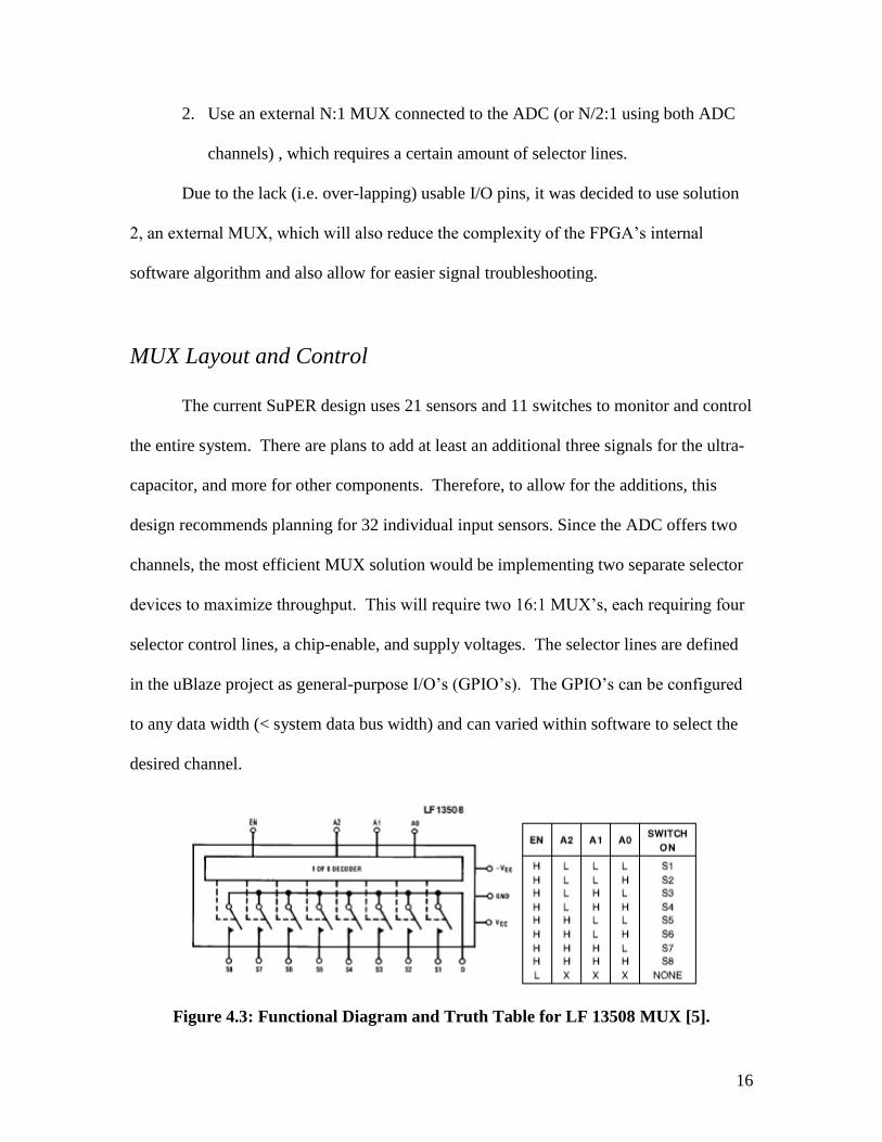
selector control lines, a chip-enable, and supply voltages. The selector lines are defined
in the uBlaze project as general-purpose I/O‟s (GPIO‟s). The GPIO‟s can be configured
to any data width (< system data bus width) and can varied within software to select the
desired channel.
Figure 4.3: Functional Diagram and Truth Table for LF 13508 MUX [5].
17
As a proof of concept, this design used an available analog MUX from the EE
department. Two LF 13508 8-channel analog multiplexers, in Figure 4.3, were acquired
and wired to a bread board that comes with the Hirose FX2-100P-1.27DS expansion
kit[3] . To show that the system can handle switching between different sensors, two
MUX input lines were connected to separate power supplies so act as voltages coming
from two separate sensors. The other MUX input lines were grounded in order to make
sure the device did not malfunction due to floating pins.
This particular MUX has a worst case switching speed of 1.8µs, therefore, an
entire sweep of all sixteen inputs causes a delay of:
16 * 1.8µs = 28.8µs
This delay can be minimized by switching the control lines in the program when
other processes are being performed that don‟t require the current value of the sensor data
such as data processing or memory writes and reads. The inputs will be simply changed
by incrementing the value of the GPIO MUX register value in software. The width is
pre-parameterized to equal to 3 and the output will follow the truth table shown above.
Once „111‟ has been sampled and stored, incrementing it will start the address back over
to „000‟.
Data Logging and Memory Control
The Spartan 3E has a Micron (MT46V32M16) 64Mbyte DDR SDRAM chip, 16-
bit data interface that can be accessed through a DDR SDRAM IP Memory Controller
core within uBlaze. Since the controller requires two fast clocks, out of sync by 180
degrees, two additional Digital Clock Managers (DCM) (Figure 4.4) are needed to

18
ensure proper timing and eliminate clock skewing. Clocking is the most important issue
facing the memory interface, and below is the clocking scheme used to connect the DDR
SDRAM Controller to memory and the FPGA.
The “External Clock” below was used as the OBP clock initially, which caused
problems due to clock lagging through the top DCM. By switching the OPB clock to the
output of the top DCM, the system resembled the recommended clocking setup more
precisely and worked accordingly. The DCM‟s also require buffers for the clock outputs
to clean up the signals before being passed to the DDR SDRAM controller. Because the
clock rate is so high, it is very susceptible to noise which can comprimise the signal.
Figure 4.4: DDR Controller Clocking Option for Asynchronous System [11]
The DDR SDRAM Controller acts as an intermediate device which connects the
OPB bus and all other necessary control lines to the on-board memory device. The
physical connections can be viewed in Appendix B, the UCF file, that uBlaze uses to
route the net signals to external pins. As aforementioned, the A/D values are 14-bit, and

19
can fit into one memory address, but offer little extra room for the time stamp. For each
sensor value, its time stamp will be stored in the address space above it. With a
maximum of 32 sensors, this leaves a total of: 32M/32 = 1M individually logged data
samples, before the DDR SDRAM is full. The address is 15-bit addressable, which
includes the two bits to signify which bank is being accessed. The memory device itself
is broken into four banks and the details of which are handled by the DDR SDRAM
Controller internally. The memory can be easily written to and read from through
assignment statements in software.
Figure 4.5: Functional Block Diagram For On-Board DDR SDRAM [4]
After initialization, which is handled by the controller, the memory goes through a
software check to ensure all addresses are being accessed and all data is being read/write

20
properly. Since the memory device is double data rate (DDR) and has a parallel
connection (Figure 4.5), the read/write times are on the order of eight clock cycles,
where the clock rate is the system clock, running at 50MHz. This will amount to a delay
of less than .2µs per memory write.
Load Switch Control and LED Verification
As with the MUX control lines, the load switch control lines are treated as
GPIO‟s that are mapped to specific I/O pins on the FPGA. These load lines act as the
MOSFET switch signals that allow the loads to turn on, while being powered by the
battery. The idea behind the design is for the on-board LED‟s to act as visual verifiers to
the status of the selected loads. The Spartan 3E comes with four on-board switches that
are active high in the up position. The user can select a desired load to be turned by
flipping a switch and the corresponding LED will illuminate. Part of the requirement is
to shut-off a load if a given threshold is reached, be it a current, voltage or temperature
warning level.
The basic algorithm takes into account the switch position and corresponding
sensor information for a particular load. If the sensor information is within safe operating
conditions, then the LED will illuminate, and the mapped I/O pin will output 3.3 V when
in the “ON” position. If the threshold is breached, then regardless of the switch position,
the LED will deactivate and MOSFET load control signal will be brought to ground, 0V.
Throughout the main polling software algorithm, the status of the switches and
corresponding sensor data will be checked and subsequently turn ON/OFF the LED‟s and
MOSFET switches accordingly.

21
At this moment, there are a five system loads and the Spartan 3E has only four
switches. For experimental purposes this offers enough user input to conduct the proof of
concept design, but will need additional hardware to be able to interface the entire SuPER
system design. The Spartan 3E I/O‟s have a switching speed of 5ns, much faster than the
system clock frequency. This ensures that when emergency shut-off levels are reached
the system will disable the MOSFET switch control lines and protect the system devices
and circuitry.
LCD User Display
The Spartan 3E Development Kit features an LCD that comes with an internal
controller with which the FPGA communicates with the display. The controller uses
three control lines and four data lines to interface with the device. Older Spartan versions
had an eight-bit data line interface; in order to communication properly, the controller is
fed two four-bit nibbles to via the data interface. The display itself is limited in size and
can handle a total of 32 characters (Figure 4.6).
Figure 4.6: Character Display Addresses Map For The LCD [3]
Therefore, the design is limited to how much information the user can display at
one time. For our purpose, the screen was split into four sections shown in Figure 4.7.

22
ADC Channel 0 Output
ADC Channel 0 From Memory
ADC Channel 1 Output
ADC Channel 0 Time Stamp
From Memory
Figure 4.7.: Sectioned LCD Screen Design
This configuration allows the designer to monitor important sensors and time
values for verification purposes. The big drawback is not allowing user input to change
the data being displayed. This is a static display design for proof of concept purposes
only. Later, the report will offer possible solutions and recommendations.

23
V. Software Integration
After building the uBlaze project with the described components above, software
must be added to make each module communicate with each other and external devices.
It produces a VHDL file that specifies names associated with each module. By using
those pre-defined names in software, the programmer can interface with each of the
components via the OPB bus. The EDK platform is capable of quickly adding pre-made
C files and header files. Each I/O pin has a specific pin value that is associated with
certain module components and GPIO. These pins are declared in the UCF and lets
uBlaze know where to be expecting the signals, while EDK takes care of all of the
routing.
Figure 5.1 shows the flow diagram for the entire system design. Most of the
modules used within uBlaze, as mentioned before, require some initialization. Appendix
C includes C files and headers in full detail with comments to explain the process better.
Included in the ISR is the pseudo MPPT algorithm, which better explains how the PWM
is changed depending on “battery” voltage levels. The start-up mode increases the duty
cycle much faster to reach normal range, where the MPPT is truly needed and most
efficient. That is why it increments using 5% steps until it reaches 35%, then the
increase/decrease step becomes about .5%. Since the ISR is entered at a frequency of 25
KHz, the small step size can still have a major effect in the overall duty cycle compared
to the systems 1/10 second polling period. The quicker the PWM can adjust to the
isolation levels of the PV array, along with battery power level, the more responsive the
DC-DC converter.

24
Main:
Initialize Timer/
Counter
to 25KHz PWM
Mode
Initialize Interrupt
Controller, LCD,
and SPI
Set LED, MUX,
and LOAD GPIO’s
as Outputs
Set SWITCH
GPIO as Input
Set Pre-Amp Gain
to -1 Via SPI Write
Enable MicroBlaze
and IntC Interrupts
Sample A/D
Channels
Process A/D
Values
Display A/D
Values on LCD
Write A/D
Value(addr = i)
and Time
Stamp(addr = i+1)
to Memory
Increment MUX by
1 and Mem. Addr
by 4
Read Back From
Memory (data and
time)
ISR
Is in Start-
Mode?
Increment
Duty Cycle by
5%
Duty Cycle
is <35%?
Switch to
Monitor
Mode
Is Battery
<1.5V?
Increment Duty
Cycle by ~.5%
1.5V <=
Battery < 2V?
Duty Cycle =
0%
Duty Cycle
Unchanged
Battery < 2.5V
Decrement
Duty Cycle by
~.5%
Clear
Interrupt Bit
Return
N
Y
Y Y Y
Y
N N N
N
Figure 5.1: Software Flow Diagram
Once all initializations are completed and interrupts are enabled, the program
enters into its polling algorithm. Here, the MUX selects the proper analog signals to pass
through to the ADC where they are sampled, processed, and stored. For user verification
purposes, those stored memory values are read back out to compare them acutal ADC
values on the LCD, along with the time stamp. The memory address MUX control lines
are then incremented before the process begins all over again.

25
VI. Testing and Verification
Sensor ADC and MUX
Two separate power supplies were connected to S0 and S15 on the MUX while
the system polled through all sixteen MUX inputs and the LCD only displayed the two
operating inputs. Table 6.1 shows the accuracy of A/D conversion and data processing
results. The actual voltage was read using an oscilloscope probe. The lower limit for the
ADC was found to be at about .78 volts, rather than .4 volts specified in the Spartan 3E
data sheet[3]. The high limit was around 2.9V, which agrees with the spec sheet.
CH 0 (V) CH 1 (V) Actual (V) %error (CH0) %error (CH1)
0.8 0.78 0.74 8.11% 5.41%
0.88 0.85 0.81 8.64% 4.94%
0.93 0.92 0.88 5.68% 4.55%
1.04 1.04 1 4.00% 4.00%
1.21 1.24 1.21 0.00% 2.48%
1.46 1.43 1.4 4.29% 2.14%
1.77 1.74 1.74 1.72% 0.00%
2.05 2.06 2.01 1.99% 2.49%
2.28 2.29 2.25 1.33% 1.78%
2.53 2.54 2.5 1.20% 1.60%
2.79 2.8 2.76 1.09% 1.45%
2.92 2.85 2.89 1.04% 1.38%
Table 6.1: A/D Conversion Accuracy
The results verify that ADC is working properly, yet there is relative error (>5%)
associated with some data points. One reason of excess error is due to the 15V analog
power supplies used in the test. They are not capable of accurate output voltages below
1V, which is seen in the lower ADC readings. As the voltages are increased, the error

26
seems to be diminished. One solution would be to use a voltage divider or potentiometer
with a constant 5V to get more accurate voltage readings from the power supplies.
Memory
The DDR SDRAM memory passed all initialization tests during the start-up of the
system. The test below in Figure 6.2 is an excerpt from the main.c software file
(Appendix C) that writes to every address and reads back from that address to verify the
proper data was stored.
for (a = 0; a < SDRAM_MAX; a++){
SDRAM[a] = a & 0xFFFF; //stores value „a‟ at address „a‟
if ((a&0xFFFF) !=SDRAM[a]) //checks each address for correct value
fail = true; //if wrong, fail = true
}
while(fail){ //displays -1, repeatedly on LCD
display_num(-1)
}
Figure 6.2: Excerpt From main.c Program For Memory Test
If this test ever fails, a „-1‟ will appear in the upper left of the LCD. The test
passed every time the program was loaded onto the board, and has yet to fail. The
variable „a‟ is masked with 0xFFFF to ensure that any data being passed to SDRAM is
only 16-bit wide. After passing the test, the program enters into the polling algorithm
where sensor data is stored, along with the time stamp, in the address above it. The LCD
verified this result as well. The value in memory matched exactly to the input voltage
applied to the ADC. The SDRAM memory appears to work and do so quickly enough to
pass the requirements stated.

27
One small glitch occurs and a fix has not been found yet. There is threshold of
around 1.6 volts and below where LCD periodically adds 130mV‟s to ADC value. Both
of those values are related to the ADC conversion equation and were factoring into the
software‟s conversion of the data. The problem was solved by introducing temporary
variables to do all data processing and manipulation. The temporay variables passed the
processed sensor data to variables that only were called by the LCD displays and memory
R/W‟s.
PWM Output
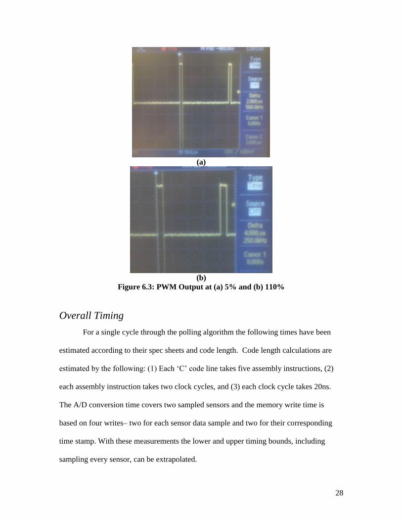
The PWM output signal performed as designed, according to the pseudo-MPPT
algorithm. In order to get a better visualization of the signal, the PWM period was
slowed down to 25Hz so measurements could be taken of the duty cycle step size.
During the start-up mode, the duty-cycle increases by 5% until 35% was reached, at
which point, by adjusting the incoming channel 0 ADC voltage, the duty cycle could be
increased or decreased by ~.25% steps. Figure 6.3 are snapshots of the PWM right at
start-up, and the increase can be seen quite clearly. The top is the initial 5% duty-cycle
followed by the next ISR iteration, (b), where the duty cycle is 10%. Furthermore, as the
voltage is raised above 2.5V, not only does the PWM duty-cycle drop to zero, the LED
corresponding to that battery load line shuts off, demonstrating the emergency shut-off
requirement was also met. The purpose was to show that a clean PWM signal can be
produced and adjusted in real-time to increase efficiency and this point was well verified.
28
(a)
(b)
Figure 6.3: PWM Output at (a) 5% and (b) 110%
Overall Timing
For a single cycle through the polling algorithm the following times have been
estimated according to their spec sheets and code length. Code length calculations are
estimated by the following: (1) Each „C‟ code line takes five assembly instructions, (2)
each assembly instruction takes two clock cycles, and (3) each clock cycle takes 20ns.
The A/D conversion time covers two sampled sensors and the memory write time is
based on four writes– two for each sensor data sample and two for their corresponding
time stamp. With these measurements the lower and upper timing bounds, including
sampling every sensor, can be extrapolated.

29
The PWM ISR contains as estimated 20 lines of code. Therefore, the PWM ISR
will take:
(20 lines) * (5 insn/line) * (2 cycle/insn) * (20 ns/cycle) = 6us
Like wise, the remainder of the polling loop contains an estimated 15 lines of code, not
including verification tests such as LCD writes and memory reads. The code is
comprismised of data processing and emergency tests. The approximated elapsed time
is:
(15 lines) * (5 insn/line) * (2 cycle/insn) * (20 ns/cycle) = 3us
As stated before, the ADC sample period is estimated at 10.25us and a memory write is
estimated at .2us per write. Table 6.2 is a summation of the software polling loop.
A/D
Conversion Memory
Writes (X4) Other Code
Polling Cycle Time
Time (us) 10.25 0.8 3 14.5
Table 6.2: Elapsed Time for a Single Poll
The lower bound, i.e. the quickest the system could sample of the sensors, can be
calculated by taking the single polling duty cycle time and multiplying it by the number
of iterations to sample the remaining sensors:
(14.5 us/sample) * (16 samples) = .232 ms
During the above elapsed time, the PWM ISR will be called every 40us, thereby being
executed:
(.232ms) / (40us) = 5.8 times,
totaling a time of:
5.8 * 6us = 34.8us

30
Table 6.3 is a summation of lowest possible limit the system can operate
approprieately.
Polling Cycle
Time Total
Sampling Time ISR Time Lower Bound
Time 14.5us 0.234ms 3.48us .267ms
Table 6.3: Lower Time Bound of System
Therefore, the system could theoretically process all of the information and
control signals in .267ms, which is well below this projects timing requirements of 1/10
of second.
On the other end of the spectrum, if the design sticks with the proposed system
duty cycle time of 1/10 of a second, the design team could take multiple samples of each
sensor and only store the average value. This idea has merit because it would store a
more accurate reading of the sensors actual value. By taking an averaging, each sensors
data is effectively smoothed out from any discrepancies or spikes that might appear in the
signals. Therefore, each sensor can be sampled approximately:
100ms/.234ms = 375 times
More testing would need to be made, of course, because this is only a preliminary
estimation according to the data gathered as of yet. The above number will turn out to be
too large for the actual system because as the complexity of the software increases, the
single polling duty cycle will as well. Yet, taking multiple samples for each sensor will
increase the reliability of the overall system and help ensure proper control of the external
devices.

31
VII. Recommendations
Though the Spartan 3E has real potential for replacing the current laptop and
other hardware, there are still a few items that need to be worked out. First, the current
data logging scheme based solely on the on-board DDR SDRAM requires attention.
Since the memory is static, data will be lost every time the system is shut-down, thereby
losing valuable experimental data. To circumvent the static memory, it would be
recommended to use an additional external non-volatile memory device that the DDR
SDRAM can dump its data into after reaching capacity. The FPGA offers a few ports
that could be interfaced to allow this transaction, but would come at a cost to the
performance of the overall system. In order to transfer the sensor data and timing
information, a new process must be implemented into software to control the operation.
This would cause a momentary lapse in the system monitoring process that could allow
for adverse consequences. It is possible to elegantly set up the “memory dump” using
interrupts instead of polling to minimize the systems break from system control.
Secondly, it is recommended that the software take multiple samples of the
sensors and then average out their values. The upper bound of 375 samples per sensor is
a little unrealistic. As mentioned before, the polling algorithm will definitely increase as
the design becomes more complicated and that upper bound will shrink. This will
ultimately save memory which, as already stated, will be an issue.
Thirdly, as stated by Mariano and Estrada [2], adding a monitor and keyboard
would offer a much better user interface. While the LCD allows for some data
verification, the size and real-time configurability can be vastly improved. In order to
look at different data, the entire project must be programmed, complied, and downloaded

32
to see the results. Adding an OS will give the user much more control via a monitor and
keyboard to actively access control algorithms and make changes without rebooting the
system, thereby losing memory data. The Spartan 3E has a PS2 and COM port already
built on, so some additional hardware would not be needed. The EDK design would need
to add a few modules, possible a UART or other communication core to interface to these
components, but overall would not affect the size or speed too much if interrupts are
used.
Lastly, the Spartan 3E has an output logic high voltage of 3.3V, which is not high
enough to drive the MOSFETS or DC-DC converter. Additional circuitry will be
required to boost the output signals to their required level by use of buffers. On the other
side, step down voltage circuits must also be made to ensure all sensor voltage levels are
within the required range of .7V-2.9V. New software must be implemented to make sure
voltage conversions are accurately calculated in reference to the MPPT algorithm and
emergency shut-off thresholds.

33
VIII. Conclusions
It was found that Spartan 3E Development Kit board is strongly suited for
reproducing the capabilities of the current laptop controlling the SuPER system. The cost
alone is a great reason to continue on with an FPGA centralized design. The Spartan 3E
evaluation board retails for around $150, compared to $600 laptop. This will bring the
price down much closer to the target price of $500. The other major system requirements
reliability and lower power consumption are satisfied. The fewer number of parts used,
the less the chance of something breaking. Reducing the number of components is
directly correlated to reducing failure. The FPGA industry has proven to produce reliable
and low power devices, and continue to improve upon the design.
The next step is to get the OS onto the FPGA. More work has been done this
quarter, but there are still many hurdles to overcome due to the lack of documentation
and experimental research. Once the FPGA has an OS, it can better emulate the laptop‟s
functionality within the system. As for now, it has been shown that the I/O abilities of
the Spartan 3E are capable of controlling all of the external components within the
system.
The research and data gathered from this project will give the next generation of
SuPER students a strong base to build upon. The major requirements are now known to
be satisfied, but some need adjustment and further investigation in regards to the
performance limits and user interface. None the less, the vision of low-cost, sustainable
energy is moving closer to reality and hopefully this, along with other SuPER research
projects can help pave the way.

34
Appendix A
Bibliography
[1] Harris, James G. “White Paper for Sustainable Power for Electrical Resources -
SuPER”
[http://courseware.ee.calpoly.edu/~jharris/research/super_project/white_paper_
super.pdf]
[2] Estrada, Brain and Mariano, Patrick “Development of UCLinux Platform for Cal Poly
SuPER Project”
[http://courseware.ee.calpoly.edu/~jharris/research/super_project/be_pm_sp.pdf]
[3] Spartan-3E Board User Guide
[http://www.xilinx.com/support/documentation/boards_and_kits/ug230.pdf]
[4] MT46V32M16 (32M x 16) DDR SDRAM Data Sheet
[http://download.micron.com/pdf/datasheets/dram/ddr/512MBDDRx4x8x16.pdf]
[5] LF 13508 MUX Data Sheet
[http://rbsfm.ej.am/Downloads/Datasheet/LF/LF13508.PDF]
[6] LTC6912 Dual Programmable Gain Amplifiers with Serial Digital Interface
[http://www.linear.com/pc/downloadDocument.do?navId=H0,C1,C1154,C1009,C
1121,P7596,D5359]
[7] Sheffield, Tyler “Cal Poly SuPER System Simulink Model and Status of Control
System”
[http://courseware.ee.calpoly.edu/~jharris/research/super_project/ts_thesis.pdf]
[8] Tal, Eran “SuPER System Prototype Design and Implementation”
[http://courseware.ee.calpoly.edu/~jharris/research/super_project/et_thesis.pdf]
[9] Joseph Witts “Cal Poly SuPER System Photovoltaic Array Universal DC-DC Step
Down Converter”
[http://courseware.ee.calpoly.edu/~jharris/research/super_project/jw_thesis.pdf]
[10] Digilient Inc. Tech Support Email
[11] MicroBlaze OPB Double Data Rate (DDR) SDRAM Controller (v2.00b)
[http://www.xilinx.com/support/documentation/ip_documentation/opb_ddr.pdf]

35
Appendix B
# UCF for SuPER Prototype Project #
# #
# Created by: Tony Wonsyld #
###################################
NET "sys_clk" LOC = "C9" ;
# No pulldown in schematic, needed here
NET "sys_reset" LOC = "K17" | PULLDOWN;
#Feedback clk for DCM
NET "fb_clk_pin" LOC = "B9" |IOSTANDARD = LVCMOS25;
NET "led_pin<7>" LOC = "F12" ; # LED 0
NET "led_pin<6>" LOC = "E12" ; # LED 1
NET "led_pin<5>" LOC = "E11" ; # LED 2
NET "led_pin<4>" LOC = "F11" ; # LED 3
NET "led_pin<3>" LOC = "C11" ; # LED 4
NET "led_pin<2>" LOC = "D11" ; # LED 5
NET "led_pin<1>" LOC = "E9" ; # LED 6
NET "led_pin<0>" LOC = "F9" ; # LED 7
NET "lcd_pin<6>" LOC = "R15" ; # LCD Data 0
NET "lcd_pin<5>" LOC = "R16" ; # LCD Data 1
NET "lcd_pin<4>" LOC = "P17" ; # LCD Data 2
NET "lcd_pin<3>" LOC = "M15" ; # LCD Data 3
NET "lcd_pin<2>" LOC = "M18" ; # LCD E
NET "lcd_pin<1>" LOC = "L18" ; # LCD RS
NET "lcd_pin<0>" LOC = "L17" ; # LCD RW
NET "spi_SCK_pin" LOC = "U16" ; #SPI clock
NET "spi_MOSI_pin" LOC = "T4" ; #SPI Write pin
NET "spi_MISO_pin" LOC = "N10" ; #SPI Read pin
NET "spi_SS_pin<0>" LOC = "P11" ; # AD_CONV for ADC
NET "spi_SS_pin<1>" LOC = "N7" ; # Preamp Chip Select
NET "spi_SS_pin<2>" LOC = "N8" ; # DAC
NET "spi_SS_pin<3>" LOC = "U3" ; # Serial Flash
NET "spi_SS_pin<4>" LOC = "C18" ; #
NET "pwm_pin" LOC = "D7" ; #PWM out signal
NET "buttons_pin<4>" LOC = "V16" | PULLDOWN ; # ROT_CENTER
NET "buttons_pin<3>" LOC = "K18" | PULLUP ; # ROT_A
NET "buttons_pin<2>" LOC = "G18" | PULLUP ; # ROT_B
NET "buttons_pin<1>" LOC = "D18" | PULLDOWN ; # BTN_WEST
NET "buttons_pin<0>" LOC = "H13" | PULLDOWN ; # BTN_EAST
NET "switches_pin<3>" LOC = "L13" | PULLUP ; #Switch 0
NET "switches_pin<2>" LOC = "L14" | PULLUP ; #Switch 1
NET "switches_pin<1>" LOC = "H18" | PULLUP ; #Switch 2
NET "switches_pin<0>" LOC = "N17" | PULLUP ; #Switch 3

36
NET "mux_pin<2>" LOC = "A6" ; #MUX controll line 0
NET "mux_pin<1>" LOC = "B6" ; #MUX controll line 1
NET "mux_pin<0>" LOC = "E7" ; #MUX controll line 2
NET "loads_pin<3>" LOC = "B4" ; #Load lines 0
NET "loads_pin<2>" LOC = "A4" ; #Load lines 1
NET "loads_pin<1>" LOC = "D5" ; #Load lines 2
NET "loads_pin<0>" LOC = "C5" ; #Load lines 3
#SRAM Addrs pins
NET "sd_a_pin<0>" LOC = "P2" | IOSTANDARD = SSTL2_I;
NET "sd_a_pin<1>" LOC = "N5" | IOSTANDARD = SSTL2_I;
NET "sd_a_pin<2>" LOC = "T2" | IOSTANDARD = SSTL2_I;
NET "sd_a_pin<3>" LOC = "N4" | IOSTANDARD = SSTL2_I;
NET "sd_a_pin<4>" LOC = "H2" | IOSTANDARD = SSTL2_I;
NET "sd_a_pin<5>" LOC = "H1" | IOSTANDARD = SSTL2_I;
NET "sd_a_pin<6>" LOC = "H3" | IOSTANDARD = SSTL2_I;
NET "sd_a_pin<7>" LOC = "H4" | IOSTANDARD = SSTL2_I;
NET "sd_a_pin<8>" LOC = "F4" | IOSTANDARD = SSTL2_I;
NET "sd_a_pin<9>" LOC = "P1" | IOSTANDARD = SSTL2_I;
NET "sd_a_pin<10>" LOC = "R2" | IOSTANDARD = SSTL2_I;
NET "sd_a_pin<11>" LOC = "R3" | IOSTANDARD = SSTL2_I;
NET "sd_a_pin<12>" LOC = "T1" | IOSTANDARD = SSTL2_I;
#SRAM data pins
NET "sd_dq_pin<0>" LOC = "H5" | IOSTANDARD = SSTL2_I;
NET "sd_dq_pin<1>" LOC = "H6" | IOSTANDARD = SSTL2_I;
NET "sd_dq_pin<2>" LOC = "G5" | IOSTANDARD = SSTL2_I;
NET "sd_dq_pin<3>" LOC = "G6" | IOSTANDARD = SSTL2_I;
NET "sd_dq_pin<4>" LOC = "F2" | IOSTANDARD = SSTL2_I;
NET "sd_dq_pin<5>" LOC = "F1" | IOSTANDARD = SSTL2_I;
NET "sd_dq_pin<6>" LOC = "E1" | IOSTANDARD = SSTL2_I;
NET "sd_dq_pin<7>" LOC = "E2" | IOSTANDARD = SSTL2_I;
NET "sd_dq_pin<8>" LOC = "M6" | IOSTANDARD = SSTL2_I;
NET "sd_dq_pin<9>" LOC = "M5" | IOSTANDARD = SSTL2_I;
NET "sd_dq_pin<10>" LOC = "M4" | IOSTANDARD = SSTL2_I;
NET "sd_dq_pin<11>" LOC = "M3" | IOSTANDARD = SSTL2_I;
NET "sd_dq_pin<12>" LOC = "L4" | IOSTANDARD = SSTL2_I;
NET "sd_dq_pin<13>" LOC = "L3" | IOSTANDARD = SSTL2_I;
NET "sd_dq_pin<14>" LOC = "L1" | IOSTANDARD = SSTL2_I;
NET "sd_dq_pin<15>" LOC = "L2" | IOSTANDARD = SSTL2_I;
#SRAM control lines
NET "sd_ba_pin<1>" LOC = "K5" | IOSTANDARD = SSTL2_I;
NET "sd_ba_pin<0>" LOC = "K6" | IOSTANDARD = SSTL2_I;
NET "sd_cas_pin" LOC = "C2" | IOSTANDARD = SSTL2_I;
NET "sd_clk_n_pin" LOC = "J4" | IOSTANDARD = SSTL2_I;
NET "sd_clk_p_pin" LOC = "J5" | IOSTANDARD = SSTL2_I;
NET "sd_cke_pin" LOC = "K3" | IOSTANDARD = SSTL2_I;
NET "sd_cs_pin" LOC = "K4" | IOSTANDARD = SSTL2_I;
NET "sd_ras_pin" LOC = "C1" | IOSTANDARD = SSTL2_I;
NET "sd_we_pin" LOC = "D1" | IOSTANDARD = SSTL2_I;
NET "sd_dqs_pin<1>" LOC = "L6" | IOSTANDARD = SSTL2_I;
NET "sd_dqs_pin<0>" LOC = "G3" | IOSTANDARD = SSTL2_I;

37
NET "sd_dm_pin<1>" LOC = "J2" | IOSTANDARD = SSTL2_I;
NET "sd_dm_pin<0>" LOC = "J1" | IOSTANDARD = SSTL2_I;
#prohibited IO's
CONFIG PROHIBIT = D2;
CONFIG PROHIBIT = G4;
CONFIG PROHIBIT = J6;
CONFIG PROHIBIT = L5;
CONFIG PROHIBIT = R4;

38
Appendix C
/*****************************************
* main.c
*
* Core program for the SuPER FPGA prototype
*
* By: Tony Wonsyld
*
*
* Purpose: Declares global variables, calls all initialization
* functions, sets up ISR, and contains polling loop
* to gather and store data.
*
*****************************************/
#include <xio.h>
#include <xparameters.h>
#include "lcd.h"
#include "outputs.h"
#include "intc.h"
#include "timer.h"
#include "spi.h"
#include "inputs.h"
unsigned int frequency = 25000; // 25kHz
unsigned int clock_freq = 50000000; // 50 MHz clock
volatile unsigned int duty_cycle = 0x62; // %5 intitial duty cycle
volatile unsigned int duty_step_start = 0x62; // %5 step size
volatile unsigned int duty_step_normal = 0x04; //~.25% step size
volatile unsigned int milli_count = 0;
volatile unsigned int milli_sec = 0;
volatile unsigned int ch_1 = 0;
volatile unsigned int ch_0 = 0;
volatile unsigned int count=0;
#define SDRAM ((volatile unsigned int *)(XPAR_DDR_MEM0_BASEADDR))
unsigned int button_array[5];
unsigned int switch_array[3];
unsigned int slow_down = 0;
/* Function prototype for ISR */
void mainISR() __attribute__((interrupt_handler));
/* mainISR: main interrupt service routine
* for the interrupt controller */
void mainISR()
{
/* If a timer interrupt is pending, run
* the timer ISR */
if(pendingIntc(XPAR_TIMER_INTERRUPT_MASK))
{ timerISR();

39
IAR = 0x03;
if (milli_count == 2500)
{ milli_sec++;
milli_count=0;
}
milli_count++;
}
}
/* main: core function to run the S3E demo */
int main(void)
{
int i=0, j=0, k=0;
unsigned char adc[5];
unsigned int status, a, b;
unsigned int button_pushed;
unsigned int fail = 0;
/* Initialize the various interfaces
* and components */
initLcd(); // Setup LCD for 4-bit communication
initSwitches(); // Set SWITCHES's to output
initLoads(); // Set LOAD lines to output's
initMux(); // Set MUX selector lines to output
initLeds(); // Set LEDs to outputs
initButtons(); // Set Buttons to inputs
initSPI(); // Setup SPI module
initIntc(); // Enable Interrupt Controller
initTimer((clock_freq / frequency) - 2, 1);
// Enable Timer. Generate interrupt
/* Turn on alternate LEDs as
* part of the S3E demo */
LEDS = 0x00;
/* Enable interrupts */
microblaze_enable_interrupts();
sendAmp(0x01, 0x01);
//Set the Pre-Amp gain to -1
writeLcd(LCD_CMD, 0x02);
//return home on LCD
MUX = 0x00; //Set initial MUX address to "000"
//Memory test
for (a = 0; a < 0x3FFFFFF; a++){
SDRAM[a] = a & 0xFFFF; //stores value address
if ((a&0xFFFF) !=SDRAM[a]) //checks each address for
fail = 1; // correct value
}
while(fail)
display_num(-1);
//if fails; displays -1 via LCD write func.
//End Memory Test

40
readSPI(SPI_ADC, adc, 5);
//dummy sample to align MEM and ADDR
for(;;) // Infinite loop
{
//microblaze_disable_interrupts();
//writeLcd(LCD_CMD, 0x02); //Move cursor to begginning
readSPI(SPI_ADC, adc, 5);
ch_0 = ((adc[0]<<8)&0x3F00) | (adc[1]&0x00FF);
if(a&0x2000) // Check sign bit
ch_0|=~0x1FFF; // Sign extend
ch_1 = ((adc[2]<<8)&0x3F00) | (adc[3]&0x00FF);
if(b&0x2000) // Check sign bit
ch_1|=~0x1FFF; // Sign extend
//Conversion to eliminate gain, offset and multiplier
ch_0 = (((-ch_0)-1)+0x2000)&0x3FFF;
ch_0 = ((ch_0)*250)/(0x3FFF)+43; //convert to mV's
ch_1 = (((-ch_1)-1)+0x2000)&0x3FFF;
ch_1 = ((ch_1)*250)/(0x3FFF)+43; //convert to mV's
//Write vaules and time stamp to SRAM
SDRAM[a] = ch_0&0xFFFF;
SDRAM[a+1] = milli_sec&0xFFFF;
SDRAM[a+2] = ch_1&0xFFFF;
SDRAM[a+3] = milli_sec&0xFFFF;
// Only display to the two channels that are applied voltages.
if(MUX == 0x00)
{
writeLcd(LCD_CMD, 0x80);
//display channel 0 value on top line of LCD
display_hex(ch_0);
for(i=0; i<5; ++i)
writeLcd(LCD_CHAR,' ');
//Move cursor over to display channel 1
display_num(ch_1);
//Display channel 1
writeLcd(LCD_CMD, 0xC0);
//Move Cursor to bottom line of LCD
//Disaplay ADC value and time stamp from SRAM
display_hex(SDRAM[a]);
for(i=0; i<5; ++i)
writeLcd(LCD_CHAR,' ');
display_num(SDRAM[a+1]);
//increase address pointer and mask
a=(a+4)&0x3FFFFFF;
writeLcd(LCD_CMD, 0x02);

41
}
MUX++; //Increase MUX address
//Emergency shut-off check and Load/LED status update
if(ch_0<250)
{
LEDS=SWITCHES;
LOADS=LEDS;
}
else
{
LEDS=SWITCHES&0x0E;
LOADS=LEDS;
}
}
return 0;
}
/*****************************************
* lcd.c
*
* LCD Main Functions
*
* By: Tony Wonsyld
*
*
* Purpose: Handles all the functions to initialize, display, and
* convert data.
*
*****************************************/
#include <xparameters.h>
#include "lcd.h"
/* readLcdStatus: gets the status from the LCD */
int readLcdStatus()
{
int i, r;
LCD_DD=LCD_DATA; // Set data lines to inputs
LCD=LCD_RW; // First read cycle (first 4 bits)
LCD=LCD_RW|LCD_E; // ~125ns
r=(LCD&LCD_DATA); // ~125ns (E high for ~250ns)
for(i=0; i<5; ++i) // Wait ~750ns
LCD=LCD_RW;
// Second read cycle (second 4 bits)
r<<=4;
LCD=LCD_RW|LCD_E; // ~125ns
r|=(LCD&LCD_DATA); // ~125ns (E high for ~250ns)
for(i=0; i<5; ++i) // Wait ~750ns
LCD=LCD_RW;
LCD_DD=0; // Set data direction back to outputs
return r&0xFF;
}

42
/* sendLcd: send the given int as an
* instruction or data (depnds on RS)
* to the LCD */
void sendLcd(int rs, int d)
{
int i;
LCD=rs;
// First write cycle
LCD=rs|LCD_E|d; // ~125ns
LCD=rs|LCD_E|d; // ~125ns total E high for ~250ns
LCD=rs|d; // ~125ns Hold time
for(i=0; i<5; ++i) // Wait ~750ns
LCD=rs;
}
/* Writes the given int to the LCD for
* both instructions and data (depends
* on RS) */
void writeLcd(int rs, int value)
{
int i, d;
/* RS is set */
if(rs)
rs=LCD_RS;
while(readLcdStatus()&LCD_BUSY);
// Wait for LCD to not be busy
sendLcd(rs, (value>>4)&LCD_DATA); // Send High nibble
sendLcd(rs, value&LCD_DATA); // Send Low nibble
for(i=0; i<10; ++i) // Wait ~1000ns
LCD=0;
}
/* initLcd: Performs the power initialization
* and entry for the LCD to read/write 8 bits */
void initLcd()
{
int i;
/* Power initialization to prepare LCD
* to read/write 8 bits as 2 4-bit nibbles */
LCD_DD=0; // Set to outputs
for(i=0; i<20*5500; ++i) LCD=0; // ~20ms delay
sendLcd(LCD_CMD, 0x03); // Set to 8-bit Operation
for(i=0; i<500; ++i) LCD=0; // ~91us delay
sendLcd(LCD_CMD, 0x03); // Set to 8-bit Operation
for(i=0; i<500; ++i) LCD=0; // ~91us delay
sendLcd(LCD_CMD, 0x03); // Set to 8-bit Operation

43
for(i=0; i<500; ++i) LCD=0; // ~91us delay
sendLcd(LCD_CMD, 0x02); // Set to 4-bit Operation
for(i=0; i<500; ++i) LCD=0; // ~91us delay
writeLcd(LCD_CMD, 0x28); // Function Set
writeLcd(LCD_CMD, 0x0C); // Display On
writeLcd(LCD_CMD, 0x01); // Clear Screen
writeLcd(LCD_CMD, 0x06); // Set Entry Mode
}
/* printLcd: Prints out the given string to
* the LCD */
void printLcd(char *msg)
{
while(*msg)
writeLcd(LCD_CHAR, *(msg++));
}
/* display_num: displays the given 4 digit number to the LCD */
void display_num(int n)
{
int i;
if(n<0)
{
writeLcd(LCD_CHAR, '-');
n=-n;
}
for(i=10000; i; i/=10)
writeLcd(LCD_CHAR, (n/i)%10 + '0');
}
#define NUMDIGITS 4
void display_hex(int n)
{
int i, v;
for(i=0; i<NUMDIGITS; ++i)
{
v=(n>>(4*((NUMDIGITS-1)-i)))&0x0F;
if(v<10)
writeLcd(LCD_CHAR, '0'+v);
else
writeLcd(LCD_CHAR, 'A'+v-10);
}
}
/***************************************
* lcd.h
*
* LCD Header File
*
* By: Tony Wonsyld
*

44
*
* Purpose: Defines registers, commands, and prototypes
* for use of the LCD
***************************************/
#ifndef LCD_H
#define LCD_H
/* Register defitions */
#define LCD (*(volatile unsigned long
*)(XPAR_LCD_BASEADDR+0x00))
// Data register
#define LCD_DD (*(volatile unsigned long
*)(XPAR_LCD_BASEADDR+0x04))
// Data direction register
/* LCD instruction and data commands */
#define LCD_DATA 0x0F
#define LCD_E 0x10
#define LCD_RS 0x20
#define LCD_RW 0x40
#define LCD_BUSY 0x80
#define LCD_CMD 0x00
#define LCD_CHAR LCD_RS
/* Function prototypes */
void initLcd();
void writeLcd(int rs, int value);
void printLcd(char *msg);
void display_num(int n);
void display_hex(int n);
#endif

45
Appendix D
1. The system clock net connections
2. ADC sample valued takes an entire sampling period before data is valid