progress in thin film solar photovoltaic technologies
TRANSCRIPT

SERIJTPa211-3604 UC Category: 270 DE89009513
Progress in Thin Film Solar Photovoltaic Technologies
H.S. Ullal K.Zweibel
December 1989
Prepared for the 9th Miami International Congress on Energy and Environment Miami Beach, Florida 11-13 December, 1989
Prepared under Task No. PV 040301
Solar Energy Research Institute A Division of Midwest Research Institute
1617 Cole Boulevard Golden, Colorado 80401-3393
Prepared for the
U.S. Department of Energy Contract No. DE-AC02 -83CH1 0093

NOTICE This report was prepared as an account of work sponsored by an agency of the United States government. Neither the United States government nor any agency thereof, nor any of their employees, makes any warranty, express or implied, or assumes any legal liability or responsibility for the accuracy, completeness, or usefulness of any information, apparatus, product, or process disclosed, or represents that its use would not infringe privately owned rights. Reference herein to any specific commercial product, process, or service by trade name, trademark, manufacturer, or otherwise does not necessarily constitute or imply its endorsement, recommendation, or favoring by the United States government or any agency thereof. The views and opinions of authors expressed herein do not necessarily state or reflect those of the United States government or any agency thereof.
Printed in the United States of America Available from:
National Technical Information Service U.S. Department of Commerce
5285 Port Royal Road Springfield, VA 22161
Price: Microfiche A01 Printed Copy A02
Codes are used for pricing all publications. The code is determined by the number of pages in the publication. Information pertaining to the pricing codes can be found in the current issue of the following publications which are generally available in most libraries: Energy Research Abstracts (ERA); Government Reports Announcements and Index ( GRA and I); Scientific and Technical Abstract Reports (STAR); and publication NTIS-PR-360 available from NTIS at the above address.

Abstract
PROGRESS IN THIN FILM SOLAR PHOTO VOLTAIC TECHNOLOGIES
Harin S. Ullal and Kenneth Zweibel Solar Energy Research Institute
1617 Cole Boulevard Golden, CO 80401, U.S.A..
(303) 231-1841
TP-3604
This paper focuses on the rapid recent advances made by thin fllm solar cell technologies, namely, amorphous silicon, copper indium diselenide, and cadmium telluride. It also indicates the several advantages of thin fllms. Various consumer products and power . applications using thin film solar cells are also discussed. The increasing interest among the utilities for PV system applications is also elucidated.
1. INTRODUCTION
The widespread utilization of photovoltaics (PV) for large-scale applications requires higher efficiency, lower-cost, and increased reliability of the devices. Accordingly, much of the research and development in the past decade has focused on high-efficiency, lowcost thin film solar cells. Other PV technologies, such as crystalline silicon, polycrystalline silicon, sheet and ribbon silicon, gallium arsenide, and concentrator solar cells are also being investigated as PV options by several research organizations [1].
This paper focuses on the rapid advances made by thin film solar cells, such as amorphous silicon (a-Si), copper indium diselehide (CuinS�, CIS), and cadmium telluride (CdTe) in the past few years. Figure 1 shows the progress of these thin film solar cell technologies.
Advantages of Thin Films
The main advantage of thin films is the minimum amount of material requirements. For example, in the crystalline silicon technology the film thickness of the cell is roughly 300 microns, whereas in the case of the thin film solar cells the film thickness is 1-3 microns. This is primarily due to the high optical absorption of thin fum materials. This reduced material requirement results in considerable cost savings. In addition, several low-cost, high throughput and scalable methods such as plasma enhanced chemical vapor deposition, electrodeposition, spraying, sputtering and selenization are available for fabricating the thin film solar cells. Also, low-cost substrates such as soda lime glass and plastic are used in large-area modules. Module fabrication is further simplified by monolithic interconnection of cells during the actual fabrication process. Thin film solar cells can also be used in both single and multijunction configurations with 15% - 20% efficiency ranges expected for optimal cell designs. Finally, the use of glass as the top encapsulant in a superstrate structure eliminates the problem of degradation of polymers such as EVA and PVB since they are not exposed to sunlight.
1

55�1,-, 2. AMORPHOUS Sll..ICON
TP-3604
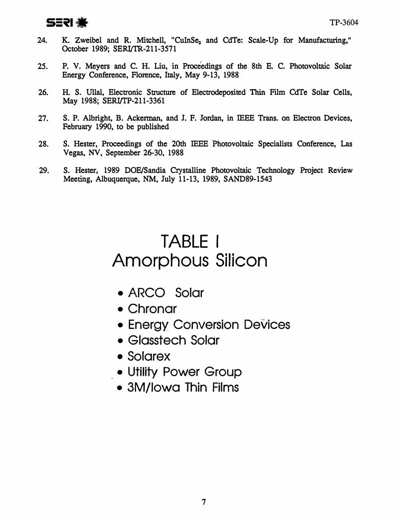
For the past several years, since the first a-Si solar cell was reported by Carlsonand Wronski in 1976 [2], there has been a great deal of progress in improving the efficiency of a-Si devices, fabricating large-area modules, and increasing the infrastructure for research and development. To-date, 26 groups around the world have reported efficiency in excess of 10% for small-area devices. The highest efficiency a-Si solar cell is a multijunction device with a conversion efficiency of 13.3% (active area) that has been fabricated by Energy Conversion Devices (BCD). The bandgaps of the three lightabsorbing layers of this device are 1.7 eV, 1.7 eV and 1.45 eV9 respectively. The top two cells are silicon based, while the bottom cell is a silicon=germanium alloy. ECD has also fabricated a 8.4% efficient square foot multijunction module using a silicon-germanium alloy. In the U.S. alone there are at least seven (7) companies that are actively involved in taking the a-Si technology from the lab to the market place. Table I summarizes the major players in this area.
In terms of technical performance, ARCO Solar has fabricated a 9.4% efficientsemitransparent single junction a-Si square-foot module with a white back reflector. Most recently, Chronar has fabricated the world's largest 2.6 ft x 5 ft single junction monolithic module (Fig. 2) with a power output of 61.76 W tested outdoors at an insolation of 1043.93 W/m2, which has been verified by SERI. The module parameters are Isc = 1.7 amperes, Voc = 57.9 volts, FF = 0.628, and Eff = 5.22%. There are 77 cells connected in series in this module, which is part of a 10 MW- Eureka project [3].
The most critical issue facing the a-Si technology is stability. Ever since the frrst report of the so-called "Staebler-Wronski" effect was published in 1977 [4], researchers have aggressively addressed this problem. Although progress has been made over the years [5], the average degradation observed in actual field testing is approximately 20% [6,7], whereas laboratory devices exhibit a 10%�15% degradation using multijunction structures. The use of multijunction device structure represents an acceptable engineering solution [8]. Most manufacturers of a-Si are engaged in research on multijunction modules which may result in cost effective thin film a-Si modules.
3. COPPER INDIUM DISELENIDE
Copper indium diselenide (CuinS�, CIS) is presently the leading thin fllm PVmaterial in terms of efficiency and reliability for terrestrial PV applications [9-12].
The fll'St 10% efficient thin film CuinS� solar cell was reported by R. A. Mickelsen and W. S. Chen of Boeing in 1982 [13]. Since then ARCO Solar, the Institute of Energy Conversion at the University of Delaware, International Solar Electric Technology, the Solar Energy Research Institute, and the University of Stuttgart have all reported efficiency over 10%. In the past few years, the rate of progress has improved dramatically at both the cell and module level. Table II lists the various deposition methods for the growth of CuinS� films. Innovative cell design, directed at improving CuinSe,. cell blue response, was first proposed by Choudary et al. [14] of ARCO Solar. It was reduced to practice by Potter et al. [15], who increased the cell efficiency to 12.5%. Further addition of Ga ( < 10%) has enhanced the cell efficiency to 14.1% (active area) for a 3.5 cm2 device alsomade by ARCO Solar [11]. Boeing has also improved their cell efficiency to 12.9% (active area) by the addition of Ga [16]. The Ga content in their device is about 27%. The most significant improvement was in the V oc of 550 m V, which is a major
improvement for this technology. Projected efficiencies for CulnS� solar cells are in the
2

TP-3604
range of 15%-20% [17,18].
Substantial technical progress has been made by ARCO Solar in the area of CulnS� module fabrication. Using the sputtering/selenization method [19 ,20], efficiency of 11.1% for a square-foot module has been verified at SERI, and 9.1% �or a four-square feet module shown in Fig. 3 with a power output of 35.8 W has been reported so far [21]. Tested outdoor for 240 days at SERI under natural sunlight under both load and opencircuit conditions, ARCO Solar's CulnSez modules have. demonstrated excellent reliability [22], as is shown in Fig. 4. This is a major accomplishment for the thin film CulnSez technology. ·
4. CADMIUM TELLURIDE
Cadmium telluride normally referred to as the "darkhorse" of thin film solar cells,has shown considerable improvement in performance in the past few years. In fact, it was
. under development before a-Si and CulnS� and made some advances in the 1970s and early 1980s.
Y.S. Tyan and E.A. Perez-Albueme of Kodak were the first to report 10% thin film CdTe solar cells in 1982 [23]. Since then several groups such as Ametek, ARCO Solar, BP Solar, Georgia Institute of Technology, Jet Propulsion Laboratory, Monosolar, International Solar Electric Technology, Photon Energy, SOHIO, Southern Methodist University, and Matsushita Battery have reported efficiencies of over 10%. A number of methods are used for depositing the CdTe thin-films, and are listed in Table III. The most promising low-cost approaches are electrodeposition and spraying. Screening printing has had limited·success so far, ·due to limitations in module processing [24].
One of the·::key technology issues for CdTe devices is the contact stability. Ametek has circumventea this problem with a novel cell design [25,26]. In this device structure, the undoped CdTe film is sandwiched between n-CdS and p-ZnTe. There is no direct metal contact to the high resistivity CdTe films. The device structure and band diagram is shown in Fig. 5 and 6, respectively. The thin film CdTe in this case is deposited by electrodeposition, a potentially low-cost technique. Using this method, Ametek has been successful in fabricating 11.2% efficient devices. Ametek has also tested their cells and modules under illumination and load, and they have reported no change in performance after 3000 hours of exposure under controlled indoor testing conditions.
Another potentially low-cost approach for fabricating large-area CdTe thin film modules is spraying. Since 1984, Photon Energy has been actively pursuing this method to manufacture product-sized photovoltaic modules [27]. In 1988, with DOE and SERI support, they made a 7.3% square-foot thin film CdTe module [Fig. 7]. They have also fabricated four-square-foot prototype CdTe mQdules. Photon Energy has very aggressive near-term goals to enter the PV power production markets. Their cost estimates suggest that they may potentially be one of the lowest cost module manufacturers. They do not appear to require the same levels of manufacturing scale-up (i.e., 10 MW) to achieve economiesof-scale. In fact, they claim that they will achieve low cost ($1-$2/W modules) at a production level of about 3 MW/year.
One of the critical issues hindering the CdTe technology is the prescence of cadmium. However, environmental issues are closely associated with "elemental Cd," but most of the processing of CdTe technology does not require elemental Cd. All processing steps can use Cd-based compounds, which are at least a 100 times safer than elemental Cd.
3
TP-3604
Manufacturers believe that Cd can be appropriately handled in the workplace. Another issue is the product disposal at the end of 30 years lifetime. A possible solution is to return the modules to smelters, who could separate out the various chemical compounds and recycle the Cd, Te, and/or glass. Several other options are also possible. It is important to realize that the amount of Cd, in these modUles is small. For instance, on the basis of producing energy, a CdTe module will produce 1 MWh for each gram of Cd, while a coal plant inadvertent releases the same amount of Cd, i.e., 1 gram/MWh (Cd present in coal). A coal plant also produces 120 gram of arsenic per MWh, as well as numerous other pollutants which are not present in PV modules. As with any strategies, one must weigh the risks and the rewards of new options against the ones o( the existing technologies they are aimed at displacing.
·
5. THIN Fll.M SOLAR CELL APPLICATIONS
Consumer Products
In the early 1980s, a number of consumer products based primarily on a-Si thin film solar cells were introduced to the market by Japanese companies. Among them, calculators, clocks, watches, etc., were the most popular products. Since then other interesting applications like battery chargers, semi-transparent car sunroofs, garden or patio lights. battery chargers for RV vehicles, and billboard lights have found increasing acceptance by consumers of the thin film solar cell based products. In fact, in 1988 a-Si products accounted for 40% of the world market share in photovoltaic shipment, primarily for consumer applications.
PV Power Applications
In the past few years, thin film solar modules have also been used for a number of solar power applications. Among them are water pumping, irrigation, street lighting, railroad signals, and small demonstration systems by utilities (4 KW - 55 KW). The most recent one is the Photovoltaics for Utility Scale Applications (PVUSA, Fig.8) projects. System sizes varying from 20 KW to 400 KW have been installed or will be installed next year at Davis. CA using a�Si. CdTe, and CulnS� for evaluation and field testing [28,29]. Thin film solar cells are making rapid progress towards helping us solve energy and environmental problems as we enter the 1990s.
6. NOMENCLATURE
A ASI a-Si a-Si:Ge a-Si:H BP Cd CdS CdTe CIS CuinS� DOE ECD
ampere(s) ARCO Solar, Inc. amorphous silicon amorphous silicon germanium hydrogenated amorphous silicon British Petroleum cadmium cadmium sulphide cadmium telluride copper indium diselenide copper indium diselenide U.S. Department of Energy Energy Conversion Devices
4

Eff EMT-1 EMT-2 EVA FF Ga GSI IEC IIC ISET JPL Jsc KW MW MWh PEl PV PVUSA Si SMU Te UPG USF US-1 voc w
Efficiency Emerging Materials Technology - 1 Emerging Materials Technology - 2 Ethylene Vinyl Acetate Fill Factor gallium Glasstech Solar, Inc. Institute of Energy Conversion short circuit current International Solar Electric Technology Jet Propulsion Laboratory short circuit current density kilowatt(s) megawatt(s) megawatt-hour Photon Energy, Inc. Photovoltaic(s) Photovoltaics for Utility Scale Applications silicon
·
Southern Methodist University tellurium Utility Power Group University of South Florida Utility Scale - 1 open circuit voltage watt(s)
Acknowledgments
TP-3604
This ·work was supported by the U.S. Department of Energy under contract # DEAC02-83CH10093.
7. REFERENCES
1. Five Year Research Plan 1987-1991, National Photovoltaics Program, U.S.Department of Energy, May 1987, DOE/CH10093-7
2. D. E. Carlson and C. R. Wronski, Appl. Phys. Lett., 2R, 671 (1976)
3. E. S. Sabisky, Z. Kiss, F. Ellis, E. Eser, S. Gau, F. Kampas, J. van Dine,and H. Weakliem, Proceedings of the 9th E. C. Photovoltaic Solar EnergyConference, Freiburg, F.R. Germany, September 25-29, 1989
4. D. L. Staebler and C. R. Wronski, Appl. Phys. Lett., ll.. 292 (1977)
5. H. S. Ullal, D. L. Morel, D. R. Willett, D. Kanani, P. C. Tyalor and C. Lee,Proceedings of the 17th IEEE Photovoltaic Specialists Conference,Kissimmee, FL, May 1-4, 1984
6. L. Mrig, Proceedings of the 24th Intersociety Energy Conversion EngineeringConference, August 6-11, 1989, Washington, D.C.
5

TP-3604
7. G. H. Atmaram and C. Herig, Proceedings of the 1989 American SolarEnergy Annual Conference, Denver, CO, June 19-22, 1989
8. W. Wallace, J. Ohi, W. Luft, B. Stafford, and E. Sabisk.y, Proceedings of the20th IEEE Photovoltaic Specialists Conference, Las Vegas, NV, September26-30, 1988
9. H. S. Ullal, K. Zweibel, and R. L. Mitchell, MRS 1989 Fall Meeting, Boston,MA, November 27 - December 2, 1989; SERI/I'P-211-3595
10. K. Zweibel, H. S. Ullal, and R. L. Mitchell, Proceedings of the 20th IEEEPhotovoltaic Specialists Conference, Las Vegas, NV, September 25-29, 19889
11. K. Zweibel and H. S. Ullal, Proceedings of the 24th Intersociety EnergyConversion Engineering Conference, Wa�hington, D.C., August 6-11, 1989
12. H. S. Ullal (Ed.), Proceedings of the Polycrystalline Thin Film ProgramMeeting, Lakewood, CO, August 16-17; SERI/CP-211-3550
13. R. A. Mickelsen and W. S. Chen, Proceedings of the 16th IEEE PhotovoltaicSpecialists Conference, San Diego, CA, September 27-30, 1982
14. U. V. Choudary, Y. H. Shing, R. R. Potter, J. R. Ermer, and V. K. Kapur,U.S. Patent No. 4,611,091, September 9, 1986
15. R. R. Potter, C. Eberspacher, L. B. Fabick, Proceedings of the 18th IEEEPhotovoltaic Specialists Conference, Las Vegas, NV, October 21-25, 1985
16. W. E. Devaney, W. S. Chen, J. M. Stewart, and R. A. Mickelsen, IEEETrans. on Electron Devices, February 1990, to be published
17. J. R. Sites, Proceedings of the 20th IEEE Photovoltaic SpecialistsConference, Las Vegas, NV, September 26-30, 1988
18. K. W. Mitchell, Proceedings of the 9th E. C. Photovoltaic Solar EnergyConference, Freiburg, F.R. Germany, September 25-29, 1989
19. R. B. Love and U. V. Choudary, U.S. Patent No. 4,465,575, August 14, 1984
20. J. R. Ermer and R. B. Love, U.S. Patent No. 4,798,660, January 17, 1989
21. J. Ermer, C. Fredric, K. Pauls, D. Pier, K. Mitchell and C. Eberspacher,Proceedings of the 4th International Photovoltaic Science and EngineeringConference, Sydney, Australia, February 14-17, 1989
22. L. Mrig and S. Rummel, in H. S. Ullal (Ed.), Proceedings of thePolycrystalline Thin Film Program Meeting, Lakewood, CO, August 16-17,1989; SERI/CP-211-3550
23. Y. S. Tyan and E. A. Perez-Albuerne, Proceedings of the 16th IEEE PhotovoltaicSpecialists Conference, San Diego, CA, September 27-30, 1982
6
TP-3604
24. K. Zweibel and R. Mitchell, "CuinSez and CdTe: Scale-Up for Manufacturing,"October 1989; SERI/I'R-211-3571
25. P. V. Meyers and C. H. Liu, in Proceedings of the 8th E. C. Photovoltaic SolarEnergy Conference, Florence, Italy, May 9-13, 1988
26. H. S. Ullal, Electronic Structure of Electrodeposited Thin Film CdTe Solar Cells,May 1988; SERI/fP-211-3361
27. S. P. Albright, B. Ackerman, and J. F. Jordan, in IEEE Trans. on Electron Devices,February 1990, to be published
28. S. Hester, Proceedings of the 20th IEEE Photovoltaic Specialists Conference, LasVegas, NV, September 26-30, 1988
29. S. Hester, 1989 DOE/Sandia Crystalline Photovoltaic Technology Project ReviewMeeting, Albuquerque, NM, July 11-13, 1989, SAND89-1543
TABLE I Amorphous Silicon
• ARCO Solar
• Chronar
• Energy Conversion Devices
• Glasstech Solar
• Solarex
. • Utility Power Group
• 3M/Iowa Thin Films
7

TABLE fl. CoinS� Processing
• Coevaporation
• Electrodeposition/selenization
• Electron beam/selenization
• Hybrid evaporation/sputtering
• Sputtering/selenization
• Reactive sputtering
• Close space vapor transport
• Metal organic chemical vapor deposition
• Sputtering/laser assisted annealing
• Sputtering/rapid isothermal processing
• Spraying
TABLE Ill CdTe Processing
• Electrodeposition • Laser assisted evaporation
• Spraying • Thermal evaporation
• Close space vapor transport • Sputtering
TP-3604
• Screen printing • Sputtering/laser assisted annealing
• Chemical vapor deposition
• Hot wall evaporation
• Ion assisted evaporation
• Molecular beam epitaxy
• Metal organic chemical vapordeposition
8

s=�•'*' TP-3604
- 16 � 0
DOE module efficiency goal (15%) cU 14CD ... as
12CD ... ::l -
10... (]) 0. as
8->. 0 c: 6CD ·a :;:
4 -CD CD ::l 2"C 0 :2 0
1980 1985 1990 0 SEAl measured
All modules 1000 cmz area or more
Figure 1 Progress in thin film solar photovoltaic module technologies
Figure 2 A 2.6 ft x S ft very large a-Si module fabricated by Chronar with a power output of 61.67 W ··
9

TP-3604
3r----------------------------------------------ZnO/CdS/CuGalnSe2/Mo/Giass
-en a. 2E Area = 3916 cm2 � -c Q) .... .... ::J 0
Figure 3
Figure 4
lsc = 2.54Amps
voc = 23.53 Volts
1 FF = 0.598 Eff = 9.1%
Power = 35.8 Watts
0�------------------------------------------_.� 0 5 10 15 20 25
Voltage (Volts)
Light I - V characteristics of a 3916 cm2 CuinSe, ARCO Solar power module with an output of 35.8 W
12r--------------------------------------- �
� CulnSe2 Modules a �w i � Load c � 8 ��====�======================== :t: Open CiFC�:Jit w 6as Area: = 1 056 cm2 e <( 4e ::J -Q) 2a. <(
0�--------------------------------� 0 40 80 120 160 200 240 280
Exposure Time (Days)
Stability performance of CuinSez modules tested outdoors at SERI under load and open circuit conditions
10

Figure 5
� ->a
� c w c e 0<D iii
TP-3604
hv� � �
) Glass ) �
0.4J..1.rT1' Sn02 ) 0.15 J..l.ffi CdS n
I 2.0J..I.m CdTe i
) 0.1 J.lffi ZnTe p ) t:o.os J..l.m Ni
Solar cell structure of a n-i-p thin film CdTe solar cell with a device configuration of Glass/SnO:JCdS/CdTe/ZnTe/Ni
OhmicContact I..-. "--..·1·------.t-·1· �p ·I
OhmicContact
I
Figure 6 Simplified band diagram of a n-i-p thin fllm CdTe solar cells
11

0.6 I CdTe Module I 0.48
�
Q) 0.36 Aperture area = 838 cm2 .... Temperature = 25°C Q)c. E 0.24
V oc = 20.5 volts � I sc = 0.52 amps FF = 0.57
0.12 Efficiency = 7.3% Pmax = 6.1 W
0 0 5 10 15 20 25
Vo lts
Figure 7 Light I � V characteristics of a 838 cm1 CdTe Photon Energy power module
Figure 8 Artist rendition of the PVUSA project at Davis, CA
12