programmable state-variable filter with wide frequency … · 2.2ghz, and q range from 2 to ......
TRANSCRIPT
Programmable State-Variable Filter with Wide
Frequency and Q Tuning Range
Alma Delić-Ibukić, Steven Mikes, Zhiguo Lai, and Dev V. Gupta Newlans, Inc., Acton, MA, USA
Email: {adelic, smikes, zlai, dgupta}@newlans.com
Abstract—This paper presents a state-variable bandpass
filter with wide frequency range coverage and wide Q
tuning range. The state-variable filter was chosen because it
can be easily extended to a universal biquad filter structure
[1]. A digital tuning technique with a novel Q-tuning
algorithm was implemented in Verilog-A, and a real-time
tuning of center frequency fc and Q was demonstrated. The
technique is accurate as long as there is no phase error in
the system. In the presence of phase error and for high Q
filter requirements, tuning algorithm based on magnitude
detection was demonstrated. A bandpass filter was
simulated in 45nm CMOS technology using RF components
for more accurate modeling of the fets. Filter simulation
results showed frequency range coverage from 520MHz to
2.2GHz, and Q range from 2 to 400. For a filter with Q=33,
simulation results showed a dynamic range of 55dB over a
3dB bandwidth at fc=1.5GHz. The current consumption of
the designed filter is 75mA at 1.2V.
Index Terms—programmable filter, calibration, biquad,
analog signal processing
I. INTRODUCTION
Programmable continuous-time universal filter
structures are still actively researched due to interest in
applications such as analog signal processing,
communication, and neural networks [2]-[6]. The most
common approach in designing tunable active filters is by
using transconductor-capacitor (Gm-C) circuits (i.e.,
integrators) [3], [4], [7]-[12]. Integrator structures
suitable for high frequencies that can provide filters with
good linearity have been reported in [8], [12]. In [8] a
tunable integrator based on inverters and suitable for GHz
applications was reported, and in [12] it was shown that
the given integrator structure can be optimized for
linearity. Also, different digital tuning techniques have
been reported [8], [13]-[15] that have shown to be
effective in tuning the center frequency fc and the quality
factor Q of the filter.
In this paper, a programmable state-variable filter with
wide frequency and Q tuning range is proposed. Such a
filter can be expanded to a universal filter structure and
cascaded to realize higher order filters. Using 45nm
CMOS technology, basic building blocks of the state-
variable filter are designed and optimized to work at high
frequencies. A novel Q-tuning algorithm is proposed and
Manuscript received April 15, 2014; revised June 27, 2014.
real-time digital tuning of fc and Q is demonstrated using
Verilog-A blocks.
This paper is organized as follows: In Section II, the
proposed state-variable filter implementation is discussed
and simulation results are presented. In Section III, the
digital tuning algorithm is discussed and simulation
results showing real-time tuning are presented. This is
followed by the summary in Section IV.
II. STATE-VARIABLE FILTER
A. Implementation
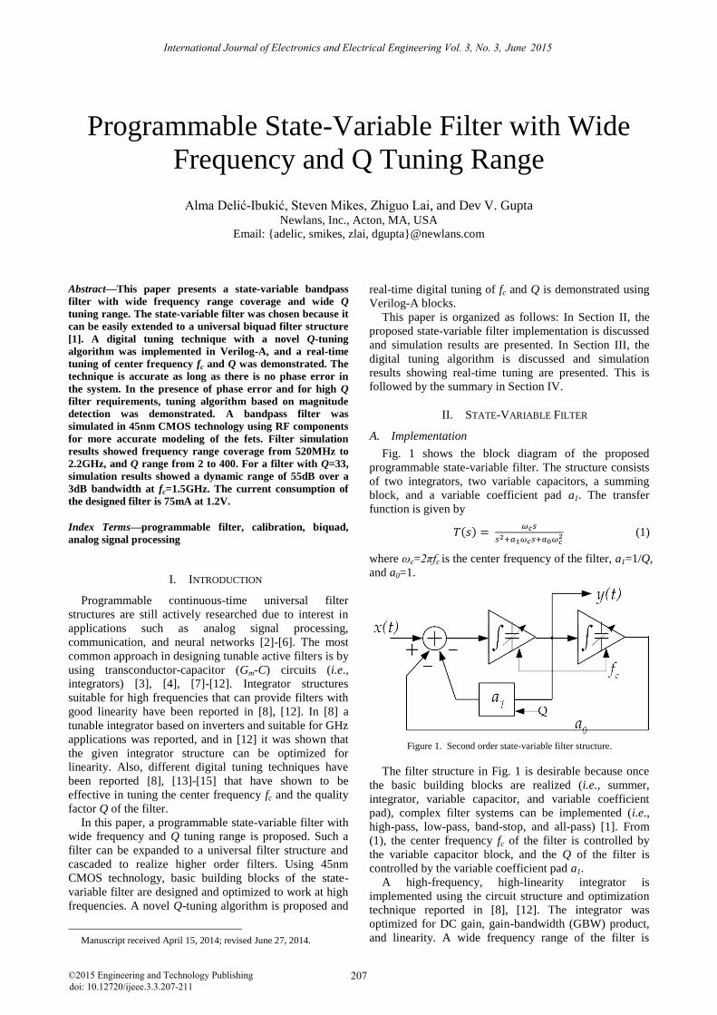
Fig. 1 shows the block diagram of the proposed
programmable state-variable filter. The structure consists
of two integrators, two variable capacitors, a summing
block, and a variable coefficient pad a1. The transfer
function is given by
( )
(1)
where ωc=2πfc is the center frequency of the filter, a1=1/Q,
and a0=1.
Figure 1. Second order state-variable filter structure.
The filter structure in Fig. 1 is desirable because once
the basic building blocks are realized (i.e., summer,
integrator, variable capacitor, and variable coefficient
pad), complex filter systems can be implemented (i.e.,
high-pass, low-pass, band-stop, and all-pass) [1]. From
(1), the center frequency fc of the filter is controlled by
the variable capacitor block, and the Q of the filter is
controlled by the variable coefficient pad a1.
A high-frequency, high-linearity integrator is
implemented using the circuit structure and optimization
technique reported in [8], [12]. The integrator was
optimized for DC gain, gain-bandwidth (GBW) product,
and linearity. A wide frequency range of the filter is
©2015 Engineering and Technology Publishing 207doi: 10.12720/ijeee.3.3.207-211
International Journal of Electronics and Electrical Engineering Vol. 3, No. 3, June 2015
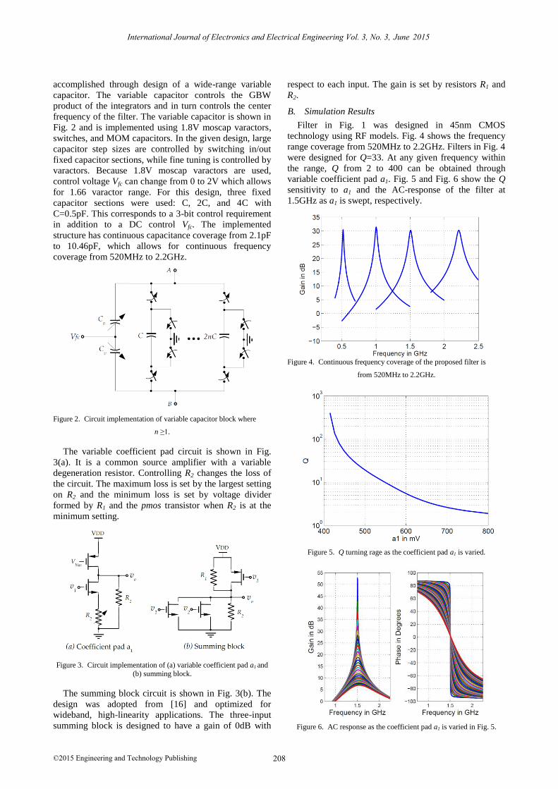
accomplished through design of a wide-range variable
capacitor. The variable capacitor controls the GBW
product of the integrators and in turn controls the center
frequency of the filter. The variable capacitor is shown in
Fig. 2 and is implemented using 1.8V moscap varactors,
switches, and MOM capacitors. In the given design, large
capacitor step sizes are controlled by switching in/out
fixed capacitor sections, while fine tuning is controlled by
varactors. Because 1.8V moscap varactors are used,
control voltage Vfc can change from 0 to 2V which allows
for 1.66 varactor range. For this design, three fixed
capacitor sections were used: C, 2C, and 4C with
C=0.5pF. This corresponds to a 3-bit control requirement
in addition to a DC control Vfc. The implemented
structure has continuous capacitance coverage from 2.1pF
to 10.46pF, which allows for continuous frequency
coverage from 520MHz to 2.2GHz.
Figure 2. Circuit implementation of variable capacitor block where
n ≥1.
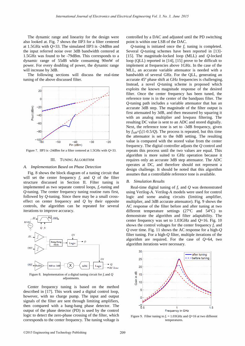
The variable coefficient pad circuit is shown in Fig.
3(a). It is a common source amplifier with a variable
degeneration resistor. Controlling R2 changes the loss of
the circuit. The maximum loss is set by the largest setting
on R2 and the minimum loss is set by voltage divider
formed by R1 and the pmos transistor when R2 is at the
minimum setting.
Figure 3. Circuit implementation of (a) variable coefficient pad a1 and
(b) summing block.
The summing block circuit is shown in Fig. 3(b). The
design was adopted from [16] and optimized for
wideband, high-linearity applications. The three-input
summing block is designed to have a gain of 0dB with
respect to each input. The gain is set by resistors R1 and
R2.
B. Simulation Results
Filter in Fig. 1 was designed in 45nm CMOS
technology using RF models. Fig. 4 shows the frequency
range coverage from 520MHz to 2.2GHz. Filters in Fig. 4
were designed for Q=33. At any given frequency within
the range, Q from 2 to 400 can be obtained through
variable coefficient pad a1. Fig. 5 and Fig. 6 show the Q
sensitivity to a1 and the AC-response of the filter at
1.5GHz as a1 is swept, respectively.
Figure 4. Continuous frequency coverage of the proposed filter is
from 520MHz to 2.2GHz.
Figure 5. Q turning rage as the coefficient pad a1 is varied.
Figure 6. AC response as the coefficient pad a1 is varied in Fig. 5.
©2015 Engineering and Technology Publishing 208
International Journal of Electronics and Electrical Engineering Vol. 3, No. 3, June 2015
The dynamic range and linearity for the design were
also looked at. Fig. 7 shows the IIP3 for a filter centered
at 1.5GHz with Q=33. The simulated IIP3 is -24dBm and
the input referred noise over 3dB bandwidth centered at
1.5GHz was found to be -79dBm. This corresponds to a
dynamic range of 55dB while consuming 90mW of
power. For every doubling of power, the dynamic range
will increase by 3dB.
The following sections will discuss the real-time
tuning of the above discussed filter.
Figure 7. IIP3 is -24dBm for a filter centered at 1.5GHz with Q=33.
III. TUNING ALGORITHM
A. Implementation Based on Phase Detection
Fig. 8 shows the block diagram of a tuning circuit that
will set the center frequency fc and Q of the filter
structure discussed in Section II. Filter tuning is
implemented as two separate control loops, fc-tuning and
Q-tuning. The center frequency tuning routine runs first,
followed by Q-tuning. Since there may be a small cross-
effect on center frequency and Q by their opposite
controls, the algorithm can be repeated for several
iterations to improve accuracy.
Figure 8. Implementation of a digital tuning circuit for fc and Q adjustments.
Center frequency tuning is based on the method
described in [17]. This work used a digital control loop,
however, with no charge pump. The input and output
signals of the filter are sent through limiting amplifiers,
then compared with a bang-bang phase detector. The
output of the phase detector (PD) is used by the control
logic to detect the zero-phase crossing of the filter, which
corresponds to the center frequency. The tuning voltage is
controlled by a DAC and adjusted until the PD switching
point is within one LSB of the DAC.
Q-tuning is initiated once the fc tuning is completed.
Several Q-tuning schemes have been reported in [13]-
[15]. The magnitude-locked loop (MLL) and Q-locked
loop (QLL) reported in [14], [15] prove to be difficult to
implement at frequencies above 1GHz. In the case of the
MLL, an accurate variable attenuator is needed with a
bandwidth of several GHz. For the QLL, generating an
accurate 45º phase shift at GHz frequencies is challenging.
Instead, a novel Q-tuning scheme is proposed which
exploits the known magnitude response of the desired
filter. Once the center frequency has been tuned, the
reference tone is in the center of the bandpass filter. The
Q-tuning path includes a variable attenuator that has an
accurate 3dB step. The magnitude of the filter output is
first attenuated by 3dB, and then measured by squaring it
with an analog multiplier and lowpass filtering. The
resulting DC value is sent to an ADC and stored digitally.
Next, the reference tone is set to -3dB frequency, given
by f3dB=fc(1-0.5/Q). The process is repeated, but this time
the attenuator is set to the 0dB setting. The resulting
value is compared with the stored value from the center
frequency. The digital controller adjusts the Q control and
repeats this process until the two values are equal. This
algorithm is more suited to GHz operation because it
requires only an accurate 3dB step attenuator. The ADC
operates at DC, and therefore should not represent a
design challenge. It should be noted that this algorithm
assumes that a controllable reference tone is available.
B. Simulation Results
Real-time digital tuning of fc and Q was demonstrated
using Verilog-A. Verilog-A models were used for control
logic and some analog circuits (limiting amplifier,
multiplier, and 3dB accurate attenuator). Fig. 9 shows the
AC response of the filter before and after tuning at two
different temperature settings (27ºC and 54ºC) to
demonstrate the algorithm and filter adaptability. The
center frequency was set to 1.03GHz and Q=16. Fig. 10
shows the control voltages for the center frequency fc and
Q over time. Fig. 11 shows the AC response for a high-Q
filter tuning. For a high-Q filter, multiple iterations of the
algorithm are required. For the case of Q=64, two
algorithm iterations were necessary.
Figure 9. Filter tuning to fc = 1.03GHz and Q=16 at two different temperatures.
©2015 Engineering and Technology Publishing 209
International Journal of Electronics and Electrical Engineering Vol. 3, No. 3, June 2015
Figure 10. Tuning algorithm settling time at two different temperatures for the filter shown in Fig. 9.
Figure 11. Filter tuning to fc=1.03GHz and Q =64.
C. Implementation and Results Based on Magnitude
Detection
The issue with the above discussed algorithm is that
the center frequency is set by using a phase detector and
searching for a zero degree phase frequency point. This
works well at low Q, but for high Q the phase error
causes significant fc and Q deviations. To mitigate this
problem, the magnitude detection for both, center
frequency and Q adjustments can be used.
Fig. 12 shows a tuning algorithm based on magnitude
detection. This requires the ability to have accurate tones
at center frequency and ±3dB frequencies. A binary
search is used to find the initial value for the variable
capacitor Vfc that sets the center frequency. At each Vfc
setting, the input tone is set to first -3dB frequency, then
to +3dB frequency. The magnitudes are compared and the
sign of the difference is used to adjust the Vfc. If the
absolute value of the difference is within a set tolerance,
the search is considered finished.
Figure 12. Implementation of a digital tuning circuit for fc and Q adjustments using magnitude detector.
To adjust the Q, the tone is swept between the three
points: f-3dB, fc, and f+3dB. Also, at fc, the 3dB attenuator is
switched on. For the correct Q the three frequencies
should agree in magnitude (or be within some specified
tolerance). If the values at f-3dB and f+3dB fall out of this
tolerance, the center frequency of the filter is assumed to
have changed (due to change in VQ), and therefore Vfc
needs to be adjusted accordingly. Initially, VQ is set to a
value known to yield a low Q, then gradually adjusted
towards higher Q settings, stopping when the correct
value is reached. This method avoids crossing into an
unstable region for the biquad.
Fig. 13 shows the AC response for the tuning
algorithm implemented using magnitude detection. The
center frequency was fixed at 1.5GHz and filter was
tuned to three different Q settings, namely 10, 50, and
100.
IV. CONCLUSION
In this paper a tunable filter with wide frequency and
Q tuning range was discussed and demonstrated. The
filter has a frequency tuning range from 520MHz to
2.2GHz and Q-tuning range from 2 to 400. Also, a digital
tuning technique (with novel Q-tuning) that accurately
sets fc and Q was discussed and demonstrated. For high Q
filters, additional tuning technique is discussed that relies
only on magnitude detection. Simulation results showed a
dynamic range of 55dB measured over the 3dB
bandwidth at the fc.
Figure 13. Filter tuning to fc = 1.5GHz and different Q values.
The discussed state-variable filter can be easily
extended to a reconfigurable universal filter structure by
introducing a set of b coefficients and an additional
summing block [1]. Furthermore, this is a voltage mode
filter which makes it ideal for cascading to obtain higher
order filter structures.
REFERENCES
[1] D. Gupta, D. V. Gupta, Z. Lai, I.-S. Shin, A. Mathew, and P. Kelly,
“State-variable wideband tunable filter,” presented at the SDR
Technical Conference and Product Exposition, Washington, DC, December 2009.
[2] D. Kamat, P. A. Mohan, and K. G. Prabhu, “Current-mode
operational transconductance amplifier-capacitor biquad filter structures based on tarmy-ghausi active-rc filter and second-order
©2015 Engineering and Technology Publishing 210
International Journal of Electronics and Electrical Engineering Vol. 3, No. 3, June 2015
digital all-pass filters,” IET Circuits, Devices, and Systems, vol. 4, pp. 346-364, Jul. 2010.
[3] M. Kumngerrn, P. Suwanjan, and K. Dejhan, “Electronically
tunable voltage mode SIMO OTA-C universal biquad filter,” in Proc. Asia-Pacific Conference on Communications, Malaysia, Oct.
2011, pp. 774-777.
[4] S. Maheshwari, S. Sing, and D. Chauhan, “Electronically tunable low-voltage mixed-mode universal filter,” IET Circuits, Devices,
and Systems, vol. 5, pp. 149-158, May 2011.
[5] S. Mahershwari, “Analog signal processing applications using a new circuit topology,” IET Circuits, Devices, and Systems, vol. 3,
pp. 106-115, Jun. 2009.
[6] H. Kuntman, “New trends in circuit design for analog signal processing,” in Proc. International Conference on Applied
Electronics, Pilsen, Sep. 2012, pp. 1-9.
[7] E. Sanchez-Sinencio and J. Silva-Martinez, “CMOS transconductance amplifiers, architectures and active filters: a
tutorial,” IEE Proceedings on Circuits, Devices, and Systems, vol.
147, pp. 3-12, Feb. 2012. [8] B. Nauta, “A CMOS transconductance-C filter technique for very
high frequencies,” IEEE Journal of Solid-State Circuits, vol. 27,
pp. 142-153, Feb. 1992. [9] A. Zjajo and M. Song, “Digitally programmable continuous time
biquad filter in 65nm CMOS,” in Proc. IEEE International
symposium on Radio-Frequency Integration Technology, Singapore, Dec. 2009, pp. 339-341.
[10] Y. Chen and Y. Zhou, “A low power CMOS mixed-integrator
based continuous time filter,” in Proc. IEEE 8th International Conference on ASIC, Changsha, Hunan, Oct. 2009, pp. 274-276.
[11] Y. Choi and H. C. Loung, “A hig-Q and wide dynamic range 70-
MHz CMOS bandpass filter for wireless receivers,” IEEE Transactions on Circuits and Systems-II, vol. 48, pp. 433-440,
May 2011.
[12] P. Crombez, J. Craninckx, P. Wambacq, and M. Steyaert, “Linearity guidelines for gm-C biquad filter design using
architecture optimization with volterra analysis,” in Proc. 18th
European Conference on Circuit Theory and Design, Seville, Aug. 2007, pp. 216-219.
[13] J.-M. Stevenson and E. Sanches-Sinencio, “An accurate quality factor tuning scheme for IF and high Q continuous time filters,”
IEEE Journal of Solid-State Circuits, vol. 33, pp. 1970-1978, Dec.
1998. [14] A. Kumar, “A wide dynamic range high-Q high-frequency
bandpass filter with an automatic quality factor tuning scheme,”
Ph.D. dissertation, Dept. Elect. And Comp. Eng., Georgia Institute of Technology, Atlanta, GA, 2009.
[15] C. S. Park and R. Schaumann, “Design of a 4-MHz analog
integrated CMOS transconductance-C bandpass filter,” IEEE Journal of Solid-State Circuits, vol. 23, pp. 987-996, Aug. 1988.
[16] A. Monpapassorn, “High frequency/low voltage CMOS adder,”
Thammasat International Journal of Science and Technology, vol. 5, pp. 49-52, May 2000.
[17] H. Liu and A. I. Karsilayan, “A high frequency bandpass
continuous-time filter with automatic frequency and Q-factor tuning,” in Proc. IEEE International Symposium on Circuits and
Systems, Sydney, NSW, May 2001, pp. 328-331.
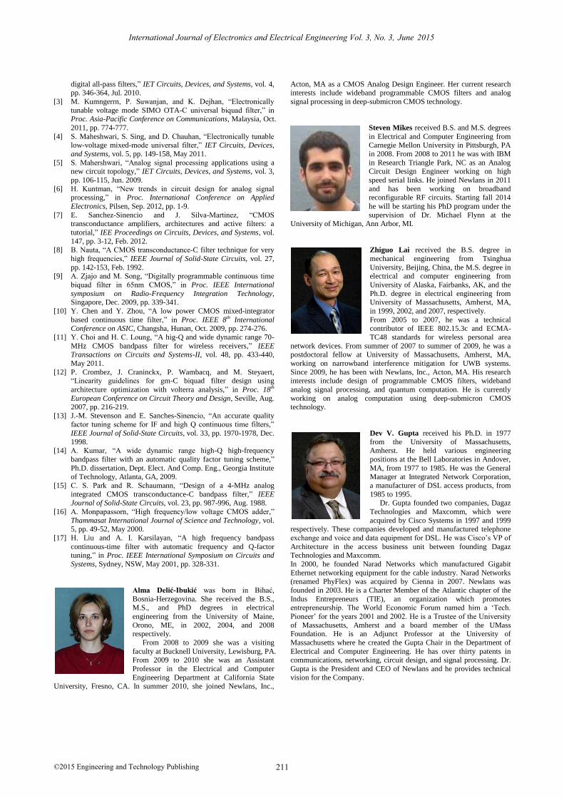
Alma Delić-Ibukić was born in Bihać,
Bosnia-Herzegovina. She received the B.S., M.S., and PhD degrees in electrical
engineering from the University of Maine,
Orono, ME, in 2002, 2004, and 2008 respectively.
From 2008 to 2009 she was a visiting
faculty at Bucknell University, Lewisburg, PA. From 2009 to 2010 she was an Assistant
Professor in the Electrical and Computer
Engineering Department at California State University, Fresno, CA. In summer 2010, she joined Newlans, Inc.,
Acton, MA as a CMOS Analog Design Engineer. Her current research interests include wideband programmable CMOS filters and analog
signal processing in deep-submicron CMOS technology.
Steven Mikes received B.S. and M.S. degrees
in Electrical and Computer Engineering from Carnegie Mellon University in Pittsburgh, PA
in 2008. From 2008 to 2011 he was with IBM
in Research Triangle Park, NC as an Analog Circuit Design Engineer working on high
speed serial links. He joined Newlans in 2011
and has been working on broadband reconfigurable RF circuits. Starting fall 2014
he will be starting his PhD program under the
supervision of Dr. Michael Flynn at the University of Michigan, Ann Arbor, MI.
Zhiguo Lai received the B.S. degree in
mechanical engineering from Tsinghua
University, Beijing, China, the M.S. degree in electrical and computer engineering from
University of Alaska, Fairbanks, AK, and the
Ph.D. degree in electrical engineering from University of Massachusetts, Amherst, MA,
in 1999, 2002, and 2007, respectively.
From 2005 to 2007, he was a technical contributor of IEEE 802.15.3c and ECMA-
TC48 standards for wireless personal area
network devices. From summer of 2007 to summer of 2009, he was a postdoctoral fellow at University of Massachusetts, Amherst, MA,
working on narrowband interference mitigation for UWB systems.
Since 2009, he has been with Newlans, Inc., Acton, MA. His research interests include design of programmable CMOS filters, wideband
analog signal processing, and quantum computation. He is currently
working on analog computation using deep-submicron CMOS technology.
Dev V. Gupta received his Ph.D. in 1977
from the University of Massachusetts, Amherst. He held various engineering
positions at the Bell Laboratories in Andover,
MA, from 1977 to 1985. He was the General Manager at Integrated Network Corporation,
a manufacturer of DSL access products, from
1985 to 1995. Dr. Gupta founded two companies, Dagaz
Technologies and Maxcomm, which were
acquired by Cisco Systems in 1997 and 1999 respectively. These companies developed and manufactured telephone
exchange and voice and data equipment for DSL. He was Cisco’s VP of
Architecture in the access business unit between founding Dagaz Technologies and Maxcomm.
In 2000, he founded Narad Networks which manufactured Gigabit
Ethernet networking equipment for the cable industry. Narad Networks (renamed PhyFlex) was acquired by Cienna in 2007. Newlans was
founded in 2003. He is a Charter Member of the Atlantic chapter of the
Indus Entrepreneurs (TIE), an organization which promotes entrepreneurship. The World Economic Forum named him a ‘Tech.
Pioneer’ for the years 2001 and 2002. He is a Trustee of the University
of Massachusetts, Amherst and a board member of the UMass Foundation. He is an Adjunct Professor at the University of
Massachusetts where he created the Gupta Chair in the Department of
Electrical and Computer Engineering. He has over thirty patents in communications, networking, circuit design, and signal processing. Dr.
Gupta is the President and CEO of Newlans and he provides technical
vision for the Company.
©2015 Engineering and Technology Publishing 211
International Journal of Electronics and Electrical Engineering Vol. 3, No. 3, June 2015