product technical specification and customer design guidelines for airprime mc8090 and mc8092
TRANSCRIPT

4110931
001
October 25, 2011
AirPrime MC8090/MC8092
Product Technical Specification
& Customer Design Guidelines

4110931 Rev 001 October 25, 2011 2
Product Technical Specification & Customer Design Guidelines
Important Notice
Safety and Hazards
Note: Some airlines may permit the use of cellular phones while the aircraft is on the ground and the door is open. Sierra Wireless modems may be used at this time.
Limitations of Liability

4110931 Rev 001 October 25, 2011 3
Product Technical Specification & Customer Design Guidelines
Patents
Copyright
Trademarks
™ ™
™ ™
Contact Information
Sales Desk:
Phone: 1-604-232-1488
Hours: 8:00 AM to 5:00 PM Pacific Time
E-mail: [email protected]
Post:
Sierra Wireless
13811 Wireless Way
Richmond, BC
Canada V6V 3A4
Fax: 1-604-231-1109
Web: www.sierrawireless.com
www.sierrawireless.com
4110931 Rev 001 October 25, 2011 4
Product Technical Specification & Customer Design Guidelines
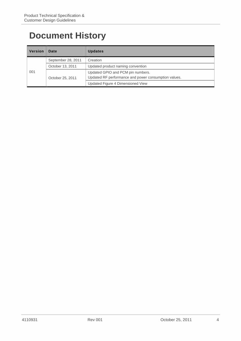
Document History
Version Date Updates
001
September 28, 2011 Creation
October 13, 2011 Updated product naming convention
October 25, 2011
Updated GPIO and PCM pin numbers.
Updated RF performance and power consumption values.
Updated Figure 4 Dimensioned View

4110931 Rev 001 October 25, 2011 5
Contents
1. INTRODUCTION ................................................................................................ 12
1.1. General Features ............................................................................................................ 12
1.2. Support Feature............................................................................................................... 16
1.3. Support Tools .................................................................................................................. 16
1.4. Accessories ..................................................................................................................... 16
1.5. Hardware Development Components ............................................................................. 16
1.6. Ordering Information ....................................................................................................... 16
1.7. Environmental Issues ...................................................................................................... 17
1.7.1. RoHS Directive Compliant ....................................................................................... 17
1.7.2. Disposing of the Product .......................................................................................... 17
2. FUNCTIONAL SPECIFICATIONS ...................................................................... 18
2.1. Functional Architecture .................................................................................................... 18
2.1.1. Chipsets ................................................................................................................... 18
2.2. Extended AT Commands ................................................................................................ 18
3. TECHNICAL SPECIFICATIONS ........................................................................ 19
3.1. Power Supply .................................................................................................................. 19
3.1.1. Burst Emission Current Requirements ..................................................................... 19
3.1.2. Power Input (VCC_3V6) ........................................................................................... 20
3.1.3. Start-up Current ....................................................................................................... 20
3.2. Decoupling of Power Supply Signals .............................................................................. 21
3.3. Mechanical Specifications ............................................................................................... 21
3.3.1. Mechanical Illustrations ............................................................................................ 21
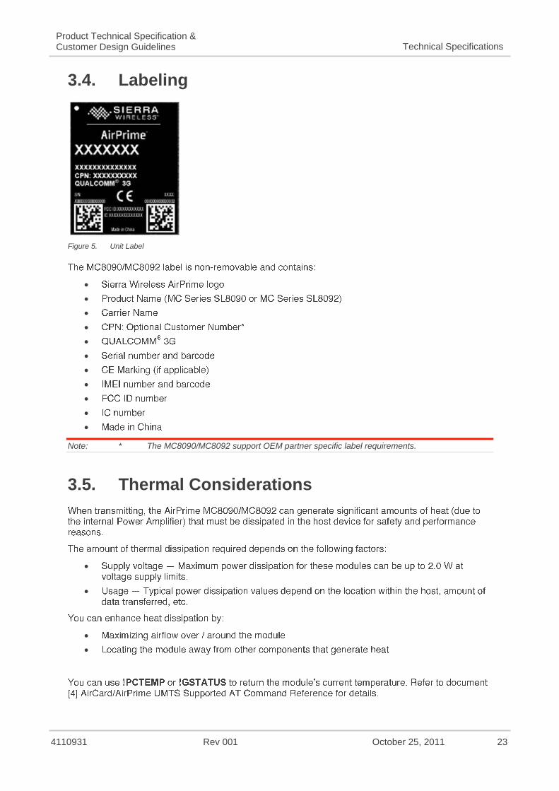
3.4. Labeling ........................................................................................................................... 23
3.5. Thermal Considerations .................................................................................................. 23
3.6. Firmware Upgrade ........................................................................................................... 24
4. INTERFACES ..................................................................................................... 25
4.1. System Design ................................................................................................................ 25
4.1.1. Pin Description ......................................................................................................... 26
4.2. Digital I/O Electrical Information ...................................................................................... 31
4.2.1. Electrical Characteristics .......................................................................................... 31
4.2.2. Pin Types ................................................................................................................. 31
4.2.3. Signal Reset States .................................................................................................. 32
4.3. General Purpose Input/Output ........................................................................................ 32
4.3.1. Pin Description ......................................................................................................... 32
4.4. Main Serial Link (UART1) ................................................................................................ 33
4.4.1. Available Services .................................................................................................... 33
4.4.2. Pin Description ......................................................................................................... 34
4.4.3. Full UART Implementation ....................................................................................... 34
4.4.4. Level Shifter Implementation.................................................................................... 35

4110931 Rev 001 October 25, 2011 6
Product Technical Specification & Customer Design Guidelines
4.4.5. Configure the UART Interface .................................................................................. 35 4.4.5.1. Low Power Operation.................................................................................................... 36
4.4.6. Lock the UART Interface .......................................................................................... 36
4.5. USIM Interface................................................................................................................. 36
4.5.1. Pin Description ......................................................................................................... 37
4.5.2. Application ................................................................................................................ 37 4.5.2.1. USIM Socket Pin Description ........................................................................................ 37
4.6. USB 2.0 Interface ............................................................................................................ 38
4.6.1. Pin Description ......................................................................................................... 38
4.6.2. Electrical Characteristics .......................................................................................... 38
4.6.3. USB Configurations .................................................................................................. 39
4.6.4. Application ................................................................................................................ 39
4.6.5. USB Host Drivers ..................................................................................................... 39 4.6.5.1. Host Driver Requirements ............................................................................................. 39
4.7. RF Interface ..................................................................................................................... 40
4.7.1. RF Connections ....................................................................................................... 40
4.7.2. RF Performance ....................................................................................................... 41
4.7.3. GPS Specifications .................................................................................................. 43 4.7.3.1. Standalone GPS ........................................................................................................... 43 4.7.3.2. gpsOneXTRA
TM ............................................................................................................ 43
4.7.3.3. A-GPS Features ............................................................................................................ 43 4.7.3.4. Enhanced Navigation 2.0 Feature ................................................................................. 44 4.7.3.5. NMEA............................................................................................................................ 44 4.7.3.6. Software ........................................................................................................................ 44
4.7.4. Antenna Specifications ............................................................................................. 44 4.7.4.1. Application .................................................................................................................... 44
4.7.5. Radiated Emissions ................................................................................................. 45
4.7.6. Radiated Sensitivity Measurement .......................................................................... 45
4.8. Digital Audio Interface (PCM) .......................................................................................... 45
4.8.1. Pin Description ......................................................................................................... 46
4.8.2. PCM Waveforms ...................................................................................................... 47
4.9. Short Message Service (SMS) ........................................................................................ 48
4.10. UMTS Radio Access Bearers Supported ........................................................................ 48
5. SIGNALS AND INDICATORS ............................................................................ 49
5.1. Reset Signal (SYSTEM_RESET_N) ............................................................................... 49
5.1.1. Pin Description ......................................................................................................... 49
5.1.2. Electrical Characteristics .......................................................................................... 50
5.1.3. Application ................................................................................................................ 50 5.1.3.1. Reset Sequence ........................................................................................................... 50 5.1.3.2. General Notes ............................................................................................................... 50
5.2. Wake Host Signal (WAKE_N) ......................................................................................... 51
5.2.1. Pin Description ......................................................................................................... 51
5.2.2. Electrical Characteristics .......................................................................................... 52
5.2.3. Application ................................................................................................................ 52
5.3. Wireless Disable Signal (W_DISABLE_N) ...................................................................... 52
5.3.1. Pin Description ......................................................................................................... 52
5.3.2. Electrical Characteristics .......................................................................................... 53
5.3.3. Application ................................................................................................................ 53 5.3.3.1. Signal Timing ................................................................................................................ 53
4110931 Rev 001 October 25, 2011 7
Product Technical Specification & Customer Design Guidelines
5.4. Flash LED (LED_FLASH) ................................................................................................ 54
5.4.1. Pin Description ......................................................................................................... 54
5.4.2. Electrical Characteristics .......................................................................................... 54
6. POWER CONSUMPTION .................................................................................. 55
6.1. Power States ................................................................................................................... 57
6.1.1. Power State Transitions ........................................................................................... 58
7. NETWORK TECHNOLOGY SPECIFICATIONS ................................................ 59
7.1. UMTS WCDMA FDD Specifications................................................................................ 59
7.2. Supported Specifications ................................................................................................. 60
7.3. UMTS (WCDMA)/GSM Specifications ............................................................................ 65
8. RELIABILITY COMPLIANCE AND RECOMMENDED STANDARDS ............... 68
8.1. Reliability Compliance ..................................................................................................... 68
8.2. Applicable Standards ...................................................................................................... 68
8.3. Environmental Specifications .......................................................................................... 69
8.3.1. Function Status Classification .................................................................................. 70
8.4. Reliability Prediction Model ............................................................................................. 70
8.4.1. Life Stress Test ........................................................................................................ 70
8.4.2. Environmental Resistance Stress Tests .................................................................. 71
8.4.3. Corrosive Resistance Stress Tests .......................................................................... 72
8.4.4. Thermal Resistance Cycle Stress Tests .................................................................. 72
8.4.5. Mechanical Resistance Stress Tests ....................................................................... 73
8.4.6. Handling Resistance Stress Tests ........................................................................... 74
9. DESIGN GUIDELINES ....................................................................................... 76
9.1. SIM Interface Routing Constraint .................................................................................... 76
9.2. EMC and ESD Recommendations .................................................................................. 76
9.3. Mechanical Integration .................................................................................................... 77
9.4. Operating System Upgrade ............................................................................................. 77
10. EMBEDDED TESTABILITY ............................................................................... 78
10.1. Testing Assistance Provided by Sierra Wireless ............................................................. 78
10.2. Integration Requirements ................................................................................................ 78
10.3. IOT/Operator ................................................................................................................... 78
10.4. Module Testing Recommendations ................................................................................. 78
10.5. Serial Link Access ........................................................................................................... 79
10.6. RF Output Accessibility ................................................................................................... 79
11. CERTIFICATION COMPLIANCE AND RECOMMENDED STANDARDS ......... 80
11.1. UMTS Compliance Acceptance and Certification ........................................................... 80
11.2. Certification Compliance ................................................................................................. 80
11.3. Applicable Standards ...................................................................................................... 81
11.3.1. Important Notice ....................................................................................................... 81

4110931 Rev 001 October 25, 2011 8
Product Technical Specification & Customer Design Guidelines
11.3.2. Safety and Hazards .................................................................................................. 81
11.3.3. Important Compliance Information for North American Users ................................. 82
11.3.4. EU Regulatory Conformity ....................................................................................... 82
12. CUSTOMIZATION .............................................................................................. 83
13. SIGNAL REFERENCE SCHEMATICS ............................................................... 84
14. REFERENCES ................................................................................................... 85
14.1. Web Site Support ............................................................................................................ 85
14.2. Reference Documents ..................................................................................................... 85
14.2.1. Sierra Wireless Documentation................................................................................ 85
14.2.2. Industry/ Other Documentation ................................................................................ 85
14.3. List of Abbreviations ........................................................................................................ 86
15. SAFETY RECOMMENDATIONS (FOR INFORMATION ONLY) ....................... 89
15.1. RF Safety ......................................................................................................................... 89
15.1.1. General ..................................................................................................................... 89
15.1.2. Exposure to RF Energy ............................................................................................ 89
15.1.3. Efficient Terminal Operation..................................................................................... 89
15.1.4. Antenna Care and Replacement .............................................................................. 89
15.2. General Safety................................................................................................................. 90
15.2.1. Driving ...................................................................................................................... 90
15.2.2. Electronic Devices .................................................................................................... 90
15.2.3. Vehicle Electronic Equipment .................................................................................. 90
15.2.4. Medical Electronic Equipment .................................................................................. 90
15.2.5. Aircraft ...................................................................................................................... 90
15.2.6. Children .................................................................................................................... 91
15.2.7. Blasting Areas .......................................................................................................... 91
15.2.8. Potentially Explosive Atmospheres .......................................................................... 91

4110931 Rev 001 October 25, 2011 9
List of Figures
Figure 1. Functional Architecture .................................................................................................... 18
Figure 2. Power Supply During Burst Emission ............................................................................. 20
Figure 3. AirPrime MC8090/MC8092 Mini Card ............................................................................ 21
Figure 4. Dimensioned View ........................................................................................................... 22
Figure 5. Unit Label ........................................................................................................................ 23
Figure 6. AirPrime MC8090/MC8092 Interface Areas .................................................................... 25
Figure 7. UART RS-232 Level Shifter Implementation ................................................................... 35
Figure 8. AirPrime MC8090/MC8092 RF Connections .................................................................. 40
Figure 9. PCM_Sync Timing ........................................................................................................... 47
Figure 10. PCM_CODEC to MC8090/MC8092 with PCM Timing .................................................... 47
Figure 11. MC8090/MC8092 with PCM to PCM_CODEC Timing .................................................... 47
Figure 12. Reset Sequence Waveform ............................................................................................ 50
Figure 13. Example of SYSTEM_RESET_N Pin Connection with Switch Configuration ................. 51
Figure 14. Example of SYSTEM_RESET_N Pin Connection with Transistor Configuration ........... 51
Figure 15. W_DISABLE_N Signal Timing ........................................................................................ 53
Figure 16. Automatic (―Triggered‖) Power State Transitions ............................................................ 58
Figure 17. Recommended Thermocouple Location ......................................................................... 79
Figure 18. USB Interface .................................................................................................................. 84
Figure 19. SIM Interface ................................................................................................................... 84

4110931 Rev 001 October 25, 2011 10
List of Tables
Table 1. Supported Bands/Connectivity ........................................................................................ 12
Table 2. MC8090/MC8092 Mini Card Features ............................................................................ 12
Table 3. Power and Ground Specifications ................................................................................... 19
Table 4. Power Supply Requirements ........................................................................................... 19
Table 5. Radio Burst Rates – Connected Mode ............................................................................ 20
Table 6. Start-up Current Peak Range .......................................................................................... 20
Table 7. Mechanical Specifications ............................................................................................... 21
Table 8. Available Interfaces and Signals ..................................................................................... 25
Table 9. AirPrime MC8090/MC8092 Pin Assignments ................................................................. 26
Table 10. Electrical Characteristics of a 1.8V Type (1V8) Digital I/O .............................................. 31
Table 11. Pin Type Codes ............................................................................................................... 31
Table 12. Reset State Definition ...................................................................................................... 32
Table 13. GPIO Interface Features ................................................................................................. 32
Table 14. GPIO Pin Description ...................................................................................................... 32
Table 15. UART1 Interface Features .............................................................................................. 33
Table 16. 4-wire UART1 Pin Description ......................................................................................... 34
Table 17. Additional Signals for an 8-wire UART ............................................................................ 34
Table 18. Configuration for Supporting a Full UART ....................................................................... 35
Table 19. USIM Interface Features ................................................................................................. 36
Table 20. USIM Pin Description ...................................................................................................... 37
Table 21. SIM Socket Pin Description ............................................................................................. 37
Table 22. USB 2.0 Interface Features ............................................................................................. 38
Table 23. USB Pin Description ........................................................................................................ 38
Table 24. USB Interface Electrical Characteristics ......................................................................... 38
Table 25. Supported USB Configurations ....................................................................................... 39
Table 26. RF Interface Features ..................................................................................................... 40
Table 27. Band Support, Conducted Tx Power and Conducted Rx Sensitivity .............................. 41
Table 28. Main RF Antenna Specification ....................................................................................... 44
Table 29. PCM Audio Interface Features ........................................................................................ 45
Table 30. Audio Pin Description ...................................................................................................... 46
Table 31. Digital Audio Interface Timing Parameters ...................................................................... 47
Table 32. Available Signals ............................................................................................................. 49
Table 33. Reset Signal Features ..................................................................................................... 49
Table 34. Reset Signal Pin Description ........................................................................................... 49
Table 35. Reset Signal Electrical Characteristics ........................................................................... 50
Table 36. Reset Settings ................................................................................................................. 51
Table 37. Wake Host Signal Features ............................................................................................. 51

4110931 Rev 001 October 25, 2011 11
Product Technical Specification & Customer Design Guidelines
Table 38. Wake Signal Pin Description ........................................................................................... 51
Table 39. Wake Signal Electrical Characteristics ............................................................................ 52
Table 40. Wireless Disable Signal Features ................................................................................... 52
Table 41. Wireless Disable Signal Pin Description ......................................................................... 52
Table 42. Wireless Disable Signal Electrical Characteristics .......................................................... 53
Table 43. W_DISABLE_N Signal Timing Parameters ..................................................................... 53
Table 44. LED Signal Features ....................................................................................................... 54
Table 45. LED_FLASH Pin Description ........................................................................................... 54
Table 46. LED_FLASH Signal Electrical Characteristics ................................................................ 54
Table 47. Averaged Standby DC Power Consumption (Preliminary/Estimated Values) ................ 55
Table 48. Averaged Call Mode Data DC Power Consumption ....................................................... 55
Table 49. Miscellaneous DC Power Consumption (Preliminary Values) ........................................ 56
Table 50. Supported GPRS/EDGE Power Classes ........................................................................ 56
Table 51. Supported MC8090/MC8092 Power States .................................................................... 57
Table 52. Power State Transitions (including voltage/temperature trigger levels) .......................... 58
Table 53. Supported WCDMA FDD Specifications ......................................................................... 59
Table 54. Supported Specifications ................................................................................................. 60
Table 55. UMTS (WCDMA)/GSM Specifications ............................................................................ 65
Table 56. Standards Conformity for the AirPrime MC8090/MC8092 Mini Card .............................. 68
Table 57. Applicable Standards and Requirements ........................................................................ 68
Table 58. Operating Class Temperature Range ............................................................................. 69
Table 59. ISO Failure Mode Severity Classification ........................................................................ 70
Table 60. Life Stress Test................................................................................................................ 70
Table 61. Environmental Resistance Stress Tests ......................................................................... 71
Table 62. Corrosive Resistance Stress Tests ................................................................................. 72
Table 63. Thermal Resistance Cycle Stress Tests ......................................................................... 72
Table 64. Mechanical Resistance Stress Tests .............................................................................. 73
Table 65. Handling Resistance Stress Tests .................................................................................. 74
Table 66. ESD Specifications .......................................................................................................... 77
Table 67. Standards Conformity for the MC8090/MC8092 Mini Card ............................................ 80
Table 68. Customizable Features ................................................................................................... 83

4110931 Rev 001 October 25, 2011 12
1. Introduction
Table 1. Supported Bands/Connectivity
Band/Connectivity MC8090 MC8092
GSM850
EGSM900
DCS1800
PCS1900
Band 1 (UMTS2100)
Band 2 (UMTS1900)
Band 5 (UMTS850)
Band 8 (UMTS900)
RX diversity Band 1 (UMTS2100)
RX diversity Band 2 (UMTS1900)
RX diversity Band 5 (UMTS850)
RX diversity Band 8 (UMTS900)
GPS (1575.42MHz)
1.1. General Features
Table 2. MC8090/MC8092 Mini Card Features
Feature Description
Physical
Small form factor—conforms to F1 as specified in PCI Express
Mini Card Electromechanical Specification Revision 1.
Three U.FL RF connector jacks
Electrical Single supply voltage (VCC) — 3.3V–4.3V
Complete body shielding — No additional shielding required
4110931 Rev 001 October 25, 2011 13
Product Technical Specification & Customer Design Guidelines Introduction
Feature Description
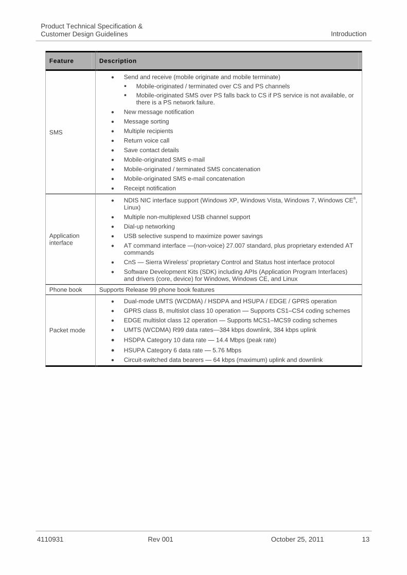
SMS
Send and receive (mobile originate and mobile terminate)
Mobile-originated / terminated over CS and PS channels
Mobile-originated SMS over PS falls back to CS if PS service is not available, or there is a PS network failure.
New message notification
Message sorting
Multiple recipients
Return voice call
Save contact details
Mobile-originated SMS e-mail
Mobile-originated / terminated SMS concatenation
Mobile-originated SMS e-mail concatenation
Receipt notification
Application interface
NDIS NIC interface support (Windows XP, Windows Vista, Windows 7, Windows CEa,
Linux)
Multiple non-multiplexed USB channel support
Dial-up networking
USB selective suspend to maximize power savings
AT command interface —(non-voice) 27.007 standard, plus proprietary extended AT commands
CnS — Sierra Wireless' proprietary Control and Status host interface protocol
Software Development Kits (SDK) including APIs (Application Program Interfaces) and drivers (core, device) for Windows, Windows CE, and Linux
Phone book Supports Release 99 phone book features
Packet mode
Dual-mode UMTS (WCDMA) / HSDPA and HSUPA / EDGE / GPRS operation
GPRS class B, multislot class 10 operation — Supports CS1–CS4 coding schemes
EDGE multislot class 12 operation — Supports MCS1–MCS9 coding schemes
UMTS (WCDMA) R99 data rates—384 kbps downlink, 384 kbps uplink
HSDPA Category 10 data rate — 14.4 Mbps (peak rate)
HSUPA Category 6 data rate — 5.76 Mbps
Circuit-switched data bearers — 64 kbps (maximum) uplink and downlink

4110931 Rev 001 October 25, 2011 14
Product Technical Specification & Customer Design Guidelines Introduction
Feature Description
Connectivity / GSM
Multiple (up to 16) cellular packet data profiles
Traditional modem COM port support for DUN, CSD, and AT commands (concurrent with NDIS)
Suspend / Resume
Sleep mode for minimum idle power draw
SIM application tool kit with proactive SIM commands
Enhanced Operator Name String (EONS)
Profile list. Typical carrier profiles are available in a drop-down list in Watcher; the user can select a profile rather than enter all the parameters.
Automatic GPRS attach at power-up
GPRS detach
Combined GPRS / IMSI detach; MS-initiated and network-initiated detach
Mobile-originated PDP context activation / deactivation
Support QoS profile
Release 99 QoS negotiation—Background, Interactive, and Streaming
Release 97—Precedence Class, Reliability Class, Delay Class, Peak Throughput, Mean Throughput
Static and Dynamic IP address. The network may assign a fixed IP address or dynamically assign one using DHCP (Dynamic Host Configuration Protocol).
PAP and CHAP support
PDP context type (IPv4). IP Packet Data Protocol context
RFC1144 TCP/IP header compression
Interaction with existing GSM services (MO/MT SMS voice calls) while:
GPRS is attached, or
In a GPRS data session (class B GPRS suspend / resume procedures)
Support for EAP-SIM authentication and PC / SC. EAP-SIM is available through:
The API
AT commands
The PC / SC interface
Voice (Digital Audio)
b
Supports:
All GSM vocoders, Enhanced Full Rate (EFR), Full Rate (FR), Half Rate (HR), and WCDMA Adaptive Multirate (AMR) encoders
MO and MT calling
Echo cancellation and noise reduction
Emergency calls (112, 110, 911, etc.)
Incoming call notification
TTY/TDD compatibility
Supplementary Services
b
Call Barring
Call Forwarding
Call Hold
Caller ID
Call Waiting
Multi-party service
USSD
4110931 Rev 001 October 25, 2011 15
Product Technical Specification & Customer Design Guidelines Introduction
Feature Description
GPS
Provides:
Standalone GPS functionality
gpsOneXTRA™
A-GPS features
NMEA support
Note: GPS specifications are preliminary targets that are subject to change without notice. Actual GPS functionality is dependent on the firmware version, and on module configuration.
Network selection
Network selection procedures described in 3G 22.011, R5 (June 2005), 3G 23.122 (June 2005), and 3G 43.022, R4
RRC connection reject message to redirect from a 3G system to a 2G system, according to 25.331, R5 (June 2004)
A CPHS Customer Service Profile-like feature [PLMN Mode bit] on a USIM / SIM that hides network selection related menus
Initial HPLMN scan at two minutes after power on
An HPLMN rescan irrespective of the serving MCC
Selective disabling of any 2G or 3G frequency band
Equivalent PLMN
Network selection generally within 30 seconds of power up
Enhanced network selection (ENS)
RF
Quad-band GSM / GPRS /EDGE (850 MHz, 900 MHz, 1800 MHz, 1900 MHz)
Dual-band UMTS WCDMA FDD
MC8092: 900 MHz, 2100 MHz
Tri-band UMTS WCDMA FDD
MC8090: 850 MHz, 1900 MHz, 2100MHz
GPS (1575.42 MHz)
Environmental
Operating temperature ranges:
Class A: -30°C to +70°C
Class B: -40°C to +85°C
Interfaces
1.8 V digital section
3 V / 1.8 V SIM interface
Serial (UART1)
Digital Audio (PCM)
USIM
USB 2.0 Slave
Operating system
Full GSM or GSM / GPRS / EGPRS operating system stack
a Contact Sierra Wireless for platform-specific Windows CE support details.
b Voice (Digital Audio)/Supplementary services on PCM variants of the MC8090/MC8092.

4110931 Rev 001 October 25, 2011 16
Product Technical Specification & Customer Design Guidelines Introduction
1.2. Support Feature
1.3. Support Tools
1.4. Accessories
1.5. Hardware Development Components
1.6. Ordering Information

4110931 Rev 001 October 25, 2011 17
Product Technical Specification & Customer Design Guidelines Introduction
1.7. Environmental Issues
1.7.1. RoHS Directive Compliant
1.7.2. Disposing of the Product

4110931 Rev 001 October 25, 2011 18
2. Functional Specifications
2.1. Functional Architecture
Figure 1. Functional Architecture
2.1.1. Chipsets
2.2. Extended AT Commands

4110931 Rev 001 October 25, 2011 19
3. Technical Specifications
3.1. Power Supply
Table 3. Power and Ground Specifications
Pin # Signal Name Type Specification Parameter Min. Typ. Max. Unit
2, 24, 39, 41, 52
VCC_3V6* V Voltage range VCC 3.30 3.60 4.30 V
4, 9, 15, 18, 21, 26, 27, 29, 34, 35, 37, 40, 43, 50
GND V - 0 - V
* Host-provided input voltage should provide 3 A instantaneous (lasting 5 ms). Refer to Table 48 Averaged Call Mode Data DC Power Consumption.
Table 4. Power Supply Requirements
Requirement Type Value
Power supply 3.6 V (nominal)
Voltage range (Vmin–Vmax) 3.3–4.3 V
Current (instantaneous (5 ms)) 3 A
Current (continuous) Refer to Table 48 Averaged Call Mode Data DC Power Consumption.
Power input capacitor(s) Add capacitance to host power rail (100 µF) to keep module operational with Vin in range.
Additional capacitance may be required if the host cannot meet the module‘s current requirements.
Conditioning capacitor (1µF, 0.1µF, 10 nF and 1 nF) recommended close to the power input for decoupling.
Note: The host must provide safe and continuous power to the mini card; the mini card does NOT have protection circuits to guard against electrical overstress.
3.1.1. Burst Emission Current Requirements

4110931 Rev 001 October 25, 2011 20
Product Technical Specification & Customer Design Guidelines Technical Specifications
Table 5. Radio Burst Rates – Connected Mode
GSM/GPRS Multislot Class
RF Power Amplifier Current
Burst Duration Period Rising Time
Class 2 (2 Rx / 1 Tx) 3.0 A peak
577 µs 4.615 ms 10 µs
Class 10 (3 Rx / 2 Tx) 1154 µs 4.615 ms
Figure 2. Power Supply During Burst Emission
3.1.2. Power Input (VCC_3V6)
µ µ
3.1.3. Start-up Current
Table 6. Start-up Current Peak Range
Current Peak at Ambient Temperature (25°C)
VCC_3V6min (3.3V)
VCC_3V6typ (3.6V)
VCC_3V6max (4.3V)
tStartup ~183mA ~177 mA ~162 mA

4110931 Rev 001 October 25, 2011 21
Product Technical Specification & Customer Design Guidelines Technical Specifications
3.2. Decoupling of Power Supply Signals
µ
3.3. Mechanical Specifications
Table 7. Mechanical Specifications
Specification Details
Form factor The MC8090/MC8092 are PCI-Express Mini Cards, comprised of an AirPrime SL809x embedded module mounted on the MC_SL adapter board.
Dimensions (nominal) Length: 50.85 mm
Width: 29.85 mm
Thickness: 4.30 mm (typical, including label thickness)
Weight: approximately 11 g
3.3.1. Mechanical Illustrations
Figure 3. AirPrime MC8090/MC8092 Mini Card

4110931 Rev 001 October 25, 2011 22
Product Technical Specification & Customer Design Guidelines Technical Specifications
Figure 4. Dimensioned View
4110931 Rev 001 October 25, 2011 23
Product Technical Specification & Customer Design Guidelines Technical Specifications
3.4. Labeling
Figure 5. Unit Label
Note: * The MC8090/MC8092 support OEM partner specific label requirements.
3.5. Thermal Considerations

4110931 Rev 001 October 25, 2011 24
Product Technical Specification & Customer Design Guidelines Technical Specifications
3.6. Firmware Upgrade

4110931 Rev 001 October 25, 2011 25
4. Interfaces
4.1. System Design
Table 8. Available Interfaces and Signals
Name Driven by AT Commands
General Purpose Input/Output
Main Serial Link (UART1) or Digital Audio Interface (PCM)
USIM Interface
USB 2.0 Interface
RF Interface
Figure 6. AirPrime MC8090/MC8092 Interface Areas

4110931 Rev 001 October 25, 2011 26
Product Technical Specification & Customer Design Guidelines Interfaces
4.1.1. Pin Description
Table 9. AirPrime MC8090/MC8092 Pin Assignments
Pin # Signal Name Description Active State Input/Output of MC8090/MC8092
Voltage (V) Type
Minimum Typical Maximum
1 NC Not connected
2 VCC_3V6 3.6 V supply Power Input 3.30 3.60 4.30 Power
3 NC Not connected
4 GND Ground GND GND - - -
5 NC Not connected
6 GPIO_0 General purpose I/O High / Low Input High 1.23 1.80 2.00 Digital
Input Low -0.30 0.59
Output High 1.25 1.80 1.90
Output Low 0 0.45
7 NC Not connected
8 EXT_VREG_USIM USIM VCC supply Power Output (1.8 V) 1.70 1.80 1.90 Power
Output (3.0 V) 2.95 3.00 3.05
9 GND Ground GND GND - - -
10 EXT_USIM_DATA USIM I/O pin Low Input High (1.8 V) 1.26 1.80 2.10 Digital
Input Low (1.8 V) 0 0.40
Output High (1.8 V) 1.26 1.80 2.10
Output Low (1.8 V) 0 0.40
Input High (3.0 V) 2.10 3.00 3.30
Input Low (3.0 V) 0 0.60

4110931 Rev 001 October 25, 2011 27
Product Technical Specification & Customer Design Guidelines Interfaces
Pin # Signal Name Description Active State Input/Output of MC8090/MC8092
Voltage (V) Type
Minimum Typical Maximum
Output High (3.0 V) 2.10 3.00 3.30
Output Low (3.0 V) 0 0.60
11 VREF_1V8 1.8 V LDO High (when module is on)
Output 1.70 1.80 1.90 Power
12 EXT_USIM_CLK USIM clock High Output High (1.8V) 1.26 1.80 2.10 Digital
Output Low (1.8V) 0 0.40
Output High (3.0V) 2.10 3.00 3.30
Output Low (3.0V) 0 0.60
13 NC Not connected
14 EXT_USIM_RESET USIM reset Low Output High (1.8V) 1.44 1.80 2.10 Digital
Output Low (1.8V) 0 0.40
Output High (3.0V) 2.40 3.00 3.30
Output Low (3.0V) 0 0.60
15 GND Ground GND GND - - -
16 NC Not connected
17 NC Not connected
18 GND Ground GND GND - - -
19 NC Not connected
20 W_DISABLE_N Wireless disable High / Low Input High 1.23 1.80 2.00 Digital
Input Low -0.30 0.59
21 GND Ground GND GND - - -
22 NC Not connected
23 NC Not connected
24 VCC_3V6 3.6 V supply Power Input 3.30 3.60 4.30 Power
25 NC Not connected
26 GND Ground GND GND - - -

4110931 Rev 001 October 25, 2011 28
Product Technical Specification & Customer Design Guidelines Interfaces
Pin # Signal Name Description Active State Input/Output of MC8090/MC8092
Voltage (V) Type
Minimum Typical Maximum
27 GND Ground GND GND - - -
28 NC Not connected
29 GND Ground GND GND - - -
30 NC Not connected
31 NC Not connected
32 WAKE_N* Wake Host Interface Low Output High 1.25 1.80 1.90 Digital
Output Low 0 0.45
33 SYSTEM_RESET_N Reset High / Low Input High 1.23 1.80 2.00 Digital
Input Low -0.30 0.59
34 GND Ground GND GND - - -
35 GND Ground GND GND - - -
36 USB_D- USB data negative (Low / Full speed)
Input High 2.00 3.30 3.60 Differential
Input Low 0 0.80
Output High 2.80 3.30 3.60
Output Low 0.30
USB data negative (High speed)
Input High 0.30 0.44
Input Low 0 0.01
Output High 0.36 0.38 0.44
Output Low 0 0.01
37 GND Ground GND GND - - -
38 USB_D+ USB data positive (Low / Full speed)
Input High 2.00 3.30 3.60 Differential
Input Low 0 0.80
Output High 2.80 3.30 3.60
Output Low 0.30
USB data positive (High speed)
Input High 0.30 0.44
Input Low 0 0.01

4110931 Rev 001 October 25, 2011 29
Product Technical Specification & Customer Design Guidelines Interfaces
Pin # Signal Name Description Active State Input/Output of MC8090/MC8092
Voltage (V) Type
Minimum Typical Maximum
Output High 0.36 0.38 0.44
Output Low 0 0.01
39 VCC_3V6 3.6 V supply Power Input 3.30 3.60 4.30 Power
40 GND Ground GND GND
41 VCC_3V6 3.6 V supply Power Input 3.30 3.60 4.30 Power
42 LED_FLASH LED driver Open Drain Output
Output Low 0 Open Drain Digital
43 GND Ground GND GND
44 GPIO_1* General purpose I/O High / Low Input High 1.23 1.80 2.00 Digital
Input Low -0.30 0.59
Output High 1.25 1.80 1.90
Output Low 0 0.45
45 UART1_CTS_N/ PCM_CLK**
UART Clear To Send/ PCM Clock
High / Low Output High 1.25 1.80 1.90 Digital
Output Low 0 0.45
46 GPIO_3* General purpose I/O High / Low Input High 1.23 1.80 2.00 Digital
Input Low -0.30 0.59
Output High 1.25 1.80 1.90
Output Low 0 0.45
47 UART1_RTS_N/ PCM_DIN**
UART Request To Send/ PCM Data In
High / Low Input High 1.23 1.80 2.00 Digital
Input Low -0.30 0.59
48 GPIO_2* General purpose I/O High / Low Input High 1.23 1.80 2.00 Digital
Input Low -0.30 0.59
Output High 1.25 1.80 1.90
Output Low 0 0.45
49 UART1_RXD/ PCM_DOUT**
UART Receive Data/ PCM Data Out
High / Low Output High 1.25 1.80 1.90 Digital
Output Low 0 0.45

4110931 Rev 001 October 25, 2011 30
Product Technical Specification & Customer Design Guidelines Interfaces
Pin # Signal Name Description Active State Input/Output of MC8090/MC8092
Voltage (V) Type
Minimum Typical Maximum
50 GND Ground GND GND
51 UART1_TXD/ PCM_SYNC**
UART Transmit Data/PCM Sync Out
High / Low Input High 1.23 1.80 2.00 Digital
Input Low -0.30 0.59
52 VCC_3V6 3.6 V supply Power Input 3.30 3.60 4.30 Power
* This pin may be reconfigured for use in a full UART implementation. Refer to section 4.4.3 Full UART Implementation for more information.
** The MC8090/MC8092 can either have PCM or UART; the function of this pin varies depending on whether the mini card is an MC8090/MC8092 with PCM or with UART.

4110931 Rev 001 October 25, 2011 31
Product Technical Specification & Customer Design Guidelines Interfaces
4.2. Digital I/O Electrical Information
4.2.1. Electrical Characteristics
Table 10. Electrical Characteristics of a 1.8V Type (1V8) Digital I/O
Parameter* I/O Type Minimum Typical Maximum Condition
Input/Output Pin
VIL CMOS -0.30 V 0.59 V
VIH CMOS 1.23 V 2.00 V
VOL CMOS 0.45 V IOL = -2 mA
VOH CMOS 1.25 V 1.90 V IOH = 2 mA
IOH 2 mA
IOL -2 mA
* ‗IL‘—Input Low; ‗IH‘—Input High; ‗OL‘—Output Low; ‗OH‘—Output High
4.2.2. Pin Types
Table 11. Pin Type Codes
Parameter Definition
A Analog pin
I Input
NP No Pull
O Digital Output
PU Pull Up
PD Pull Down
V Power or Ground pin

4110931 Rev 001 October 25, 2011 32
Product Technical Specification & Customer Design Guidelines Interfaces
4.2.3. Signal Reset States
Table 12. Reset State Definition
Parameter Definition
0 Set to GND
1 Set to supply 1V8
Pull-down Internal pull-down with ~60 kΩ resistor (TBD)
Pull-up Internal pull-up with ~60 kΩ resistor to supply 1V8 (TBD)
Z High impedance
Undefined Caution: Undefined must not be used in an application if a special state is required at reset. These pins may be toggling a signal(s) during reset.
4.3. General Purpose Input/Output
Table 13. GPIO Interface Features
Feature Details
Purpose OEM-configurable general purpose I/O (control, signaling, monitoring, etc.)
Implementation Defaults to digital output
Power 1.8V (use VREF_1V8 as logic reference)
Output drive current up to 2 mA.
Note: These pins can only be used as either GPIO or additional UART pins.
4.3.1. Pin Description
Table 14. GPIO Pin Description
Pin # Signal Name I/O Type Reset State Description
46 GPIO_3* 1V8
Configurable general purpose I/O 48 GPIO_2* 1V8
44 GPIO_1* 1V8
6 GPIO_0 1V8
* This pin may be reconfigured for use in a full UART implementation. Refer to section 4.4.3 Full UART Implementation for more information.

4110931 Rev 001 October 25, 2011 33
Product Technical Specification & Customer Design Guidelines Interfaces
Caution: Sierra Wireless reserves the right to dedicate any of these pins for specific purposes in the future. Use at your own risk.
4.4. Main Serial Link (UART1)
Note: MC8090/MC8092 with UART mini cards may be provisioned with the ability to use the UART interface to communicate with peripheral devices. Contact Sierra Wireless for further information.
Table 15. UART1 Interface Features
Feature Details
Purpose Serial host–module communication
Dependent on provisioning, communication with peripheral devices. Contact Sierra Wireless for further information.
Implementation Four-wire serial interface based on TIA-232 (RS232 protocol)
An RS-232 level shifter device may be required, as described in section 4.4.4 Level Shifter Implementation.
Optional full UART configuration as described in section 4.4.3 Full UART Implementation.
Data rates supported High speed (up to 4 Mbps)
Optional functionality Dependent on provisioning, module may be able to communicate with peripheral devices. Contact Sierra Wireless to discuss possible firmware support.
Note: This interface is NOT AVAILABLE in the MC8090/MC8092 with PCM variants.
4.4.1. Available Services
–
4110931 Rev 001 October 25, 2011 34
Product Technical Specification & Customer Design Guidelines Interfaces
4.4.2. Pin Description
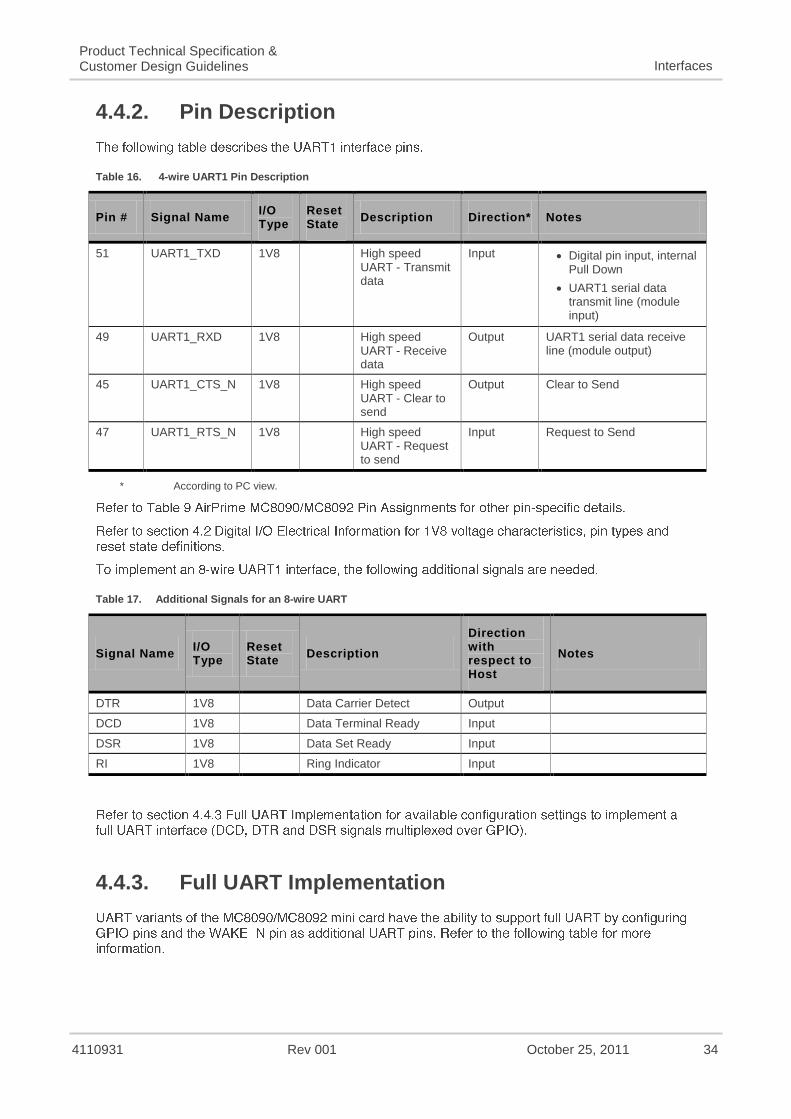
Table 16. 4-wire UART1 Pin Description
Pin # Signal Name I/O Type
Reset State
Description Direction* Notes
51 UART1_TXD 1V8 High speed UART - Transmit data
Input Digital pin input, internal Pull Down
UART1 serial data transmit line (module input)
49 UART1_RXD 1V8 High speed UART - Receive data
Output UART1 serial data receive line (module output)
45 UART1_CTS_N 1V8 High speed UART - Clear to send
Output Clear to Send
47 UART1_RTS_N 1V8 High speed UART - Request to send
Input Request to Send
* According to PC view.
Table 17. Additional Signals for an 8-wire UART
Signal Name I/O Type
Reset State
Description
Direction with respect to Host
Notes
DTR 1V8 Data Carrier Detect Output
DCD 1V8 Data Terminal Ready Input
DSR 1V8 Data Set Ready Input
RI 1V8 Ring Indicator Input
4.4.3. Full UART Implementation

4110931 Rev 001 October 25, 2011 35
Product Technical Specification & Customer Design Guidelines Interfaces
Table 18. Configuration for Supporting a Full UART
Additional UART Signal GPIO Pins Used for an Extended UART Configuration
Signal Name Function Value Pin # Signal Name Function
DCD Data Carrier Detect 1V8 output 44 GPIO_1 General Purpose I/O
DTR Data Terminal Ready 1V8 input 48 GPIO_2 General Purpose I/O
DSR Data Set Ready 1V8 output 46 GPIO_3 General Purpose I/O
RI Ring Indicator 1V8 output 32 WAKE_N Wake Host Interface
4.4.4. Level Shifter Implementation
Figure 7. UART RS-232 Level Shifter Implementation
Note: The U1 chip also protects the AirPrime MC8090/MC8092 mini card against ESD at 15kV (air discharge).
4.4.5. Configure the UART Interface

4110931 Rev 001 October 25, 2011 36
Product Technical Specification & Customer Design Guidelines Interfaces
4.4.5.1. Low Power Operation
4.4.6. Lock the UART Interface
4.5. USIM Interface
Table 19. USIM Interface Features
Feature Details
Purpose Communicate with USIM socket on host device
Implementation Four-wire interface
Voltage levels comply with 3GPP standards
Power 1.8 V (3G) or 3.0 V (2G) operation. Compliant with GSM 11.11 recommendations concerning SIM functions.
Host must keep current draw 10mA

4110931 Rev 001 October 25, 2011 37
Product Technical Specification & Customer Design Guidelines Interfaces
4.5.1. Pin Description
Table 20. USIM Pin Description
Pin # Signal Name I/O Type
Description Notes
8 EXT_VREG_USIM USIM power supply 1.8 V (3G) or 3 V (2G).
Maximum allowed current draw = 10 mA.
14 EXT_USIM_RESET USIM reset signal
10 EXT_USIM_DATA USIM data Requires a 15–25 kΩ pull-up resistor to EXT_VREG_USIM.
Filtering cap in pF range may be needed.
12 EXT_USIM_CLK USIM clock Typically 4 MHz at EXT_VREG_USIM level.
Host should minimize rise time (< 50 ns) by adjusting trace capacitance and filtering needs as required.
4.5.2. Application
4.5.2.1. USIM Socket Pin Description
Table 21. SIM Socket Pin Description
Pin # Signal Name Description
1 VCC EXT_ VREG_USIM
2 RST EXT_USIM_RESET
3 CLK EXT_USIM_CLK
4 - -
5 GND GROUND
6 - -
7 I/O EXT_USIM_DATA
8 - -
4110931 Rev 001 October 25, 2011 38
Product Technical Specification & Customer Design Guidelines Interfaces
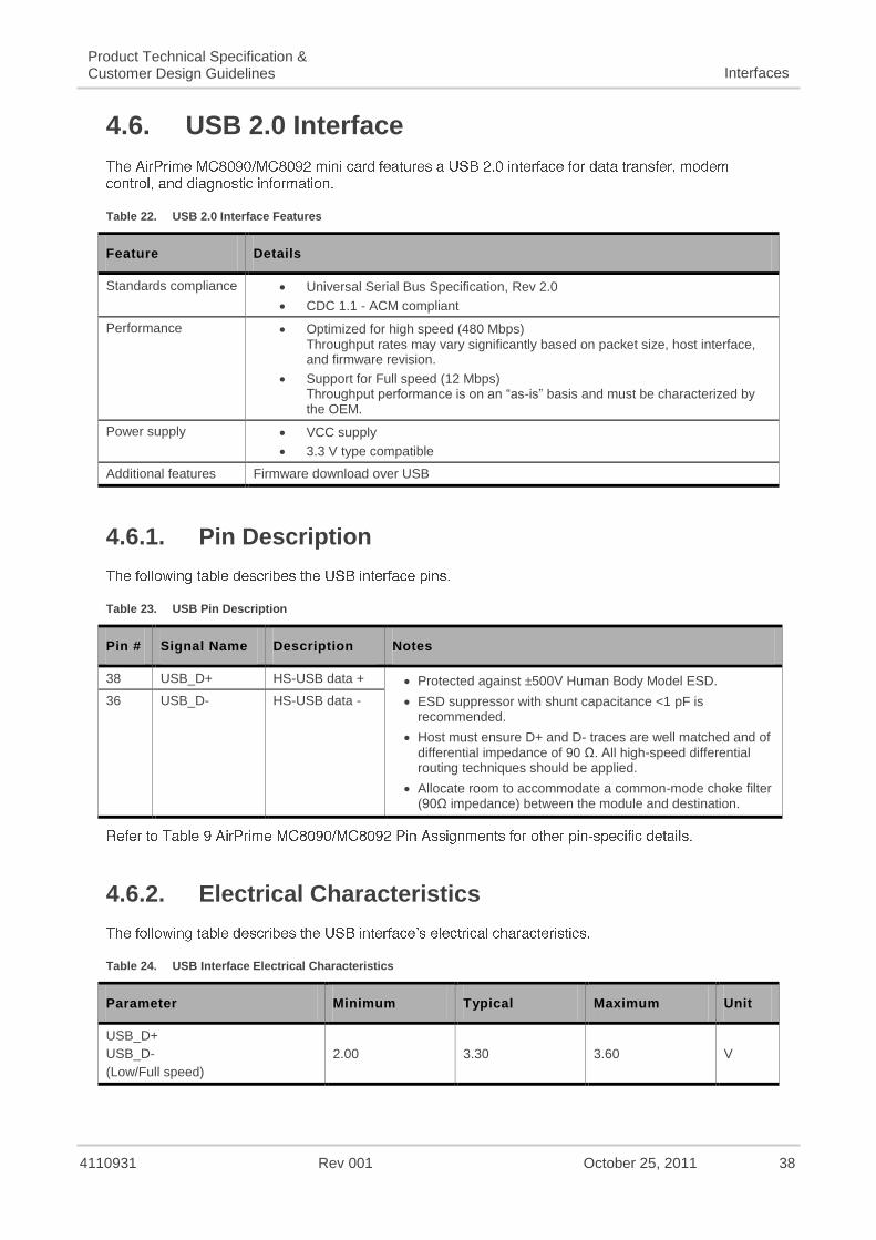
4.6. USB 2.0 Interface
Table 22. USB 2.0 Interface Features
Feature Details
Standards compliance Universal Serial Bus Specification, Rev 2.0
CDC 1.1 - ACM compliant
Performance Optimized for high speed (480 Mbps) Throughput rates may vary significantly based on packet size, host interface, and firmware revision.
Support for Full speed (12 Mbps) Throughput performance is on an ―as-is‖ basis and must be characterized by the OEM.
Power supply VCC supply
3.3 V type compatible
Additional features Firmware download over USB
4.6.1. Pin Description
Table 23. USB Pin Description
Pin # Signal Name Description Notes
38 USB_D+ HS-USB data + Protected against ±500V Human Body Model ESD.
ESD suppressor with shunt capacitance <1 pF is recommended.
Host must ensure D+ and D- traces are well matched and of differential impedance of 90 Ω. All high-speed differential routing techniques should be applied.
Allocate room to accommodate a common-mode choke filter (90Ω impedance) between the module and destination.
36 USB_D- HS-USB data -
4.6.2. Electrical Characteristics
Table 24. USB Interface Electrical Characteristics
Parameter Minimum Typical Maximum Unit
USB_D+
USB_D-
(Low/Full speed)
2.00 3.30 3.60 V

4110931 Rev 001 October 25, 2011 39
Product Technical Specification & Customer Design Guidelines Interfaces
Parameter Minimum Typical Maximum Unit
USB_D+
USB_D-
(High speed)
0.30 0.38 0.44 V
4.6.3. USB Configurations
Table 25. Supported USB Configurations
Configuration Interfaces Services
Composite, Direct IP OBEX, ACM, ECM CnS, DM, NMEA, AT, DIP data
Composite, MUX-capable OBEX, ACM CnS, DM, NMEA, AT, PPP data
Composite OBEX, ACM CnS, DM, NMEA, AT, PPP data
Non-composite, MUX-capable OBEX, ACM CnS, DM, NMEA, AT, PPP data
4.6.4. Application
4.6.5. USB Host Drivers
4.6.5.1. Host Driver Requirements

4110931 Rev 001 October 25, 2011 40
Product Technical Specification & Customer Design Guidelines Interfaces
4.7. RF Interface
Table 26. RF Interface Features
Feature Details
Purpose Primary antenna — Tx / Rx
Diversity antenna — Rx
GPS antenna — GPS functionality
Impedance Nominal: 50Ω
DC: High Impedance
4.7.1. RF Connections
Figure 8. AirPrime MC8090/MC8092 RF Connections
Ω
Note: If the antenna connection is shorted or open, the modem will not sustain permanent damage.

4110931 Rev 001 October 25, 2011 41
Product Technical Specification & Customer Design Guidelines Interfaces
4.7.2. RF Performance
Table 27. Band Support, Conducted Tx Power and Conducted Rx Sensitivity
Band Frequencies (MHz) MC8090 MC8092 Conducted Tx Power Conducted Rx Sensitivity (dBm)
Average (dBm) Notes
GSM Bands Coding Mode Typical Worst Case
GSM 850 Tx: 824 - 849
Rx: 869 - 894
+33 ± 2 GMSK, connectorized (Class 4) CS1-3a
CS4b
MCS1-3c
MCS4c
MCS5c
MCS6c
MCS7c
MCS8c
MCS9c
GMSK
GMSK
GMSK
GMSK
8PSK
8PSK
8PSK
8PSK
8PSK
-106
-103
-106
-103.5
-100
-98
-95
-92.5
-90
-102
-99
-102
-99.5
-96
-94
-91
-88.5
-86
+27 ± 3 8PSK, connectorized (Class E2)
EGSM 900 Tx: 880 - 915
Rx: 925 - 960
+33 ± 2 GMSK, connectorized (Class 4)
+27 ± 3 8PSK, connectorized (Class E2)
DCS 1800 Tx: 1710 - 1785
Rx: 1805 - 1880
+30 ± 2 GMSK, connectorized (Class 1)
+26 ± 3 8PSK, connectorized (Class E2)
PCS 1900 Tx: 1850 - 1910
Rx: 1930 - 1990
+30 ± 2 GMSK, connectorized (Class 1)
+26 ± 3 8PSK, connectorized (Class E2)
WCDMA Bands Call Details Typical Worst Case
Band I
WCDMA 2100
Tx: 1920–1980
Rx: 2110–2170
+24 +1/-3 Connectorized (Class 3)
Nominal conditions
RMC DL 12.2 kbps; 0.1% BER
-107.5 -106.7
Band II
WCDMA 1900
Tx: 1850–1910
Rx: 1930–1990
-107 -104.7
Band V
WCDMA 850
Tx: 824–849
Rx: 869–894
-108 -104.7
Band VIII
WCDMA 900
Tx: 880–915
Rx: 925–960
-108 -103.7
WCDMA Bands RX Diversity

4110931 Rev 001 October 25, 2011 42
Product Technical Specification & Customer Design Guidelines Interfaces
Band Frequencies (MHz) MC8090 MC8092 Conducted Tx Power Conducted Rx Sensitivity (dBm)
Average (dBm) Notes
Band I
WCDMA 2100
Tx: 1920 – 1980
Rx: 2110 – 2170
RMC DL 12.2 kbps; 0.1% BER
-107.5 -106.7
Band II
WCDMA 1900
Tx: 1850 – 1910
Rx: 1930 – 1990
-107 -104.7
Band V
WCDMA 850
Tx: 824 – 849
Rx: 869 – 894
-108 -104.7
Band VIII
WCDMA 900
Tx: 880 – 915
Rx: 925 – 960
-108 -103.7
GPS
GPS 1575.42
a 2% Bit Error Rate (BER) circuit switched
b 10% Block Error Rate (BLER)
c WCDMA channel spacing is 5 MHz, but this can be adjusted to optimize performance in a particular deployment scenario.

4110931 Rev 001 October 25, 2011 43
Product Technical Specification & Customer Design Guidelines Interfaces
4.7.3. GPS Specifications
Note: These specifications are preliminary targets that are subject to change without notice. Actual GPS functionality depends on the firmware version and module configuration.
4.7.3.1. Standalone GPS
Note: For optimum performance, the modem should be registered on the GSM/UMTS network, but does not need to be on an active data or voice call.
4.7.3.2. gpsOneXTRATM
4.7.3.3. A-GPS Features

4110931 Rev 001 October 25, 2011 44
Product Technical Specification & Customer Design Guidelines Interfaces
4.7.3.4. Enhanced Navigation 2.0 Feature
4.7.3.5. NMEA
4.7.3.6. Software
4.7.4. Antenna Specifications
Table 28. Main RF Antenna Specification
Parameter Minimum Typical Maximum Unit Description
Cable loss - - 0.5 dB Maximum loss to antenna
Impedance - 50 - Ω Antenna load impedance
VSWR - - 1.6:1 Maximum allowed VSWR of antenna
Radiated gain 0 dBi In one direction at least
Note: Sierra Wireless recommends a maximum VSWR of 1.6:1 for both TX and RX bands.
4.7.4.1. Application

4110931 Rev 001 October 25, 2011 45
Product Technical Specification & Customer Design Guidelines Interfaces
4.7.5. Radiated Emissions
Ω
4.7.6. Radiated Sensitivity Measurement
4.8. Digital Audio Interface (PCM)
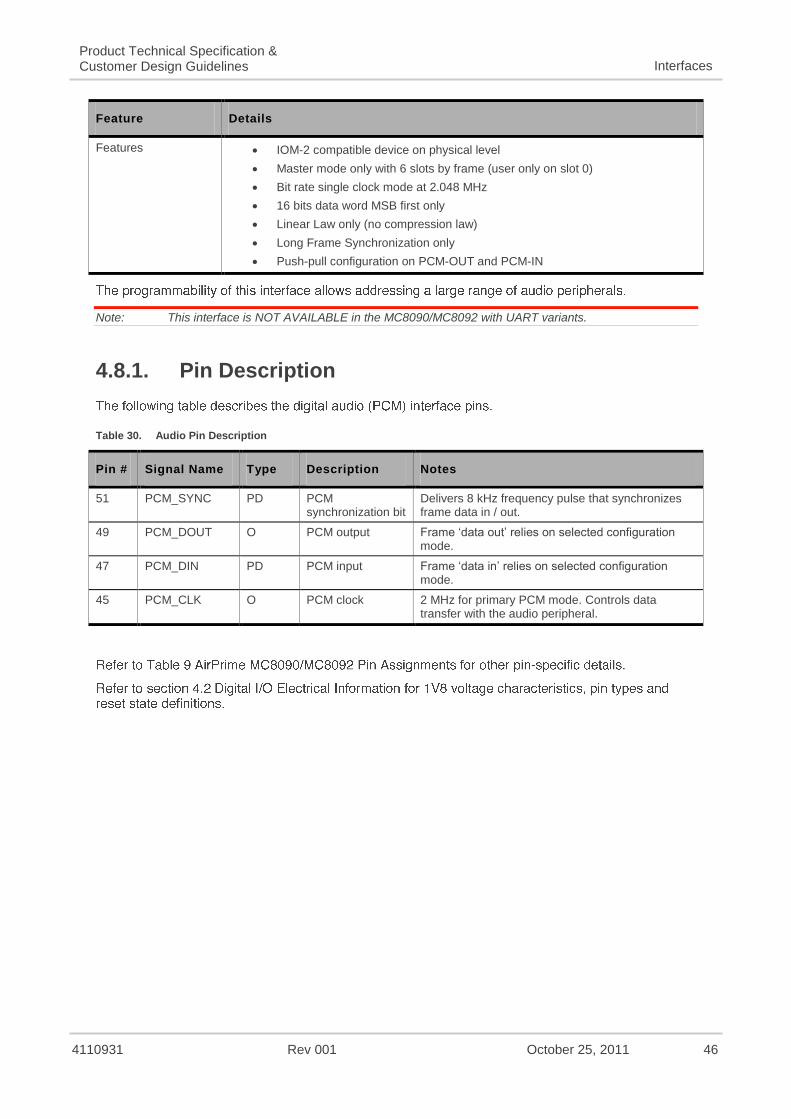
Table 29. PCM Audio Interface Features
Feature Details
Implementation Primary PCM supported to interface with external codec
Power 1.8 V (use VREF_1V8 as logic reference)
4110931 Rev 001 October 25, 2011 46
Product Technical Specification & Customer Design Guidelines Interfaces
Feature Details
Features IOM-2 compatible device on physical level
Master mode only with 6 slots by frame (user only on slot 0)
Bit rate single clock mode at 2.048 MHz
16 bits data word MSB first only
Linear Law only (no compression law)
Long Frame Synchronization only
Push-pull configuration on PCM-OUT and PCM-IN
Note: This interface is NOT AVAILABLE in the MC8090/MC8092 with UART variants.
4.8.1. Pin Description
Table 30. Audio Pin Description
Pin # Signal Name Type Description Notes
51 PCM_SYNC PD PCM synchronization bit
Delivers 8 kHz frequency pulse that synchronizes frame data in / out.
49 PCM_DOUT O PCM output Frame ‗data out‘ relies on selected configuration mode.
47 PCM_DIN PD PCM input Frame ‗data in‘ relies on selected configuration mode.
45 PCM_CLK O PCM clock 2 MHz for primary PCM mode. Controls data transfer with the audio peripheral.

4110931 Rev 001 October 25, 2011 47
Product Technical Specification & Customer Design Guidelines Interfaces
4.8.2. PCM Waveforms
Figure 9. PCM_Sync Timing
Figure 10. PCM_CODEC to MC8090/MC8092 with PCM Timing
Figure 11. MC8090/MC8092 with PCM to PCM_CODEC Timing
Table 31. Digital Audio Interface Timing Parameters
Signal Description Minimum Typical Maximum Unit
Tsync_low + Tsync_high
PCM-SYNC period 125 µs
Tsync_low PCM-SYNC low time 124.5 µs
Tsync_high PCM-SYNC high time 400 500 ns
TSYNC_CLK PCM-SYNC to PCM-CLK time 60 ns
TCLK-cycle PCM-CLK period 488 ns

4110931 Rev 001 October 25, 2011 48
Product Technical Specification & Customer Design Guidelines Interfaces
Signal Description Minimum Typical Maximum Unit
TIN-setup PCM-IN setup time 50 ns
TIN-hold PCM-IN hold time 10 ns
TOUT-delay PCM-OUT delay time 350 ns
4.9. Short Message Service (SMS)
4.10. UMTS Radio Access Bearers Supported

4110931 Rev 001 October 25, 2011 49
5. Signals and Indicators
Table 32. Available Signals
Name Driven by AT Commands
Reset Signal (SYSTEM_RESET_N)
Wake Host Signal (WAKE_N)
Wireless Disable Signal (W_DISABLE_N)
Flash LED (LED_FLASH)
5.1. Reset Signal (SYSTEM_RESET_N)
Note: An operating system reset is preferred to a hardware reset.
Table 33. Reset Signal Features
Feature Details
Purpose Used by host to reset the module
Implementation
Digital input. 1.8 V logic (active low)
The MC8090/MC8092 has been provided with a 10 kΩ internal pull-up resistor (to module-provided 1.8 V reference (pin 11 — VREF_1V8)).
Caution: This signal should only be used for EMERGENCY resets.
5.1.1. Pin Description
Table 34. Reset Signal Pin Description
Pin # Signal Name I/O I/O Type Description
33 SYSTEM_RESET_N I 1V8 MC8090/MC8092 reset
4110931 Rev 001 October 25, 2011 50
Product Technical Specification & Customer Design Guidelines Signals and Indicators
5.1.2. Electrical Characteristics
Table 35. Reset Signal Electrical Characteristics
Parameter Minimum Typical Maximum Unit
SYSTEM_RESET_N time (Rt)a 30 ms
SYSTEM_RESET_N time (Rt)b at power up
only 10 20 30 ms
VIL 0.59 V
VIH 1.23 V
a This reset time is the minimum to be carried out on the SYSTEM_RESET_N signal when the power supply is already stabilized.
b This reset time is internally carried out by the mini card power supply supervisor only when the mini card power supplies are powered ON.
5.1.3. Application
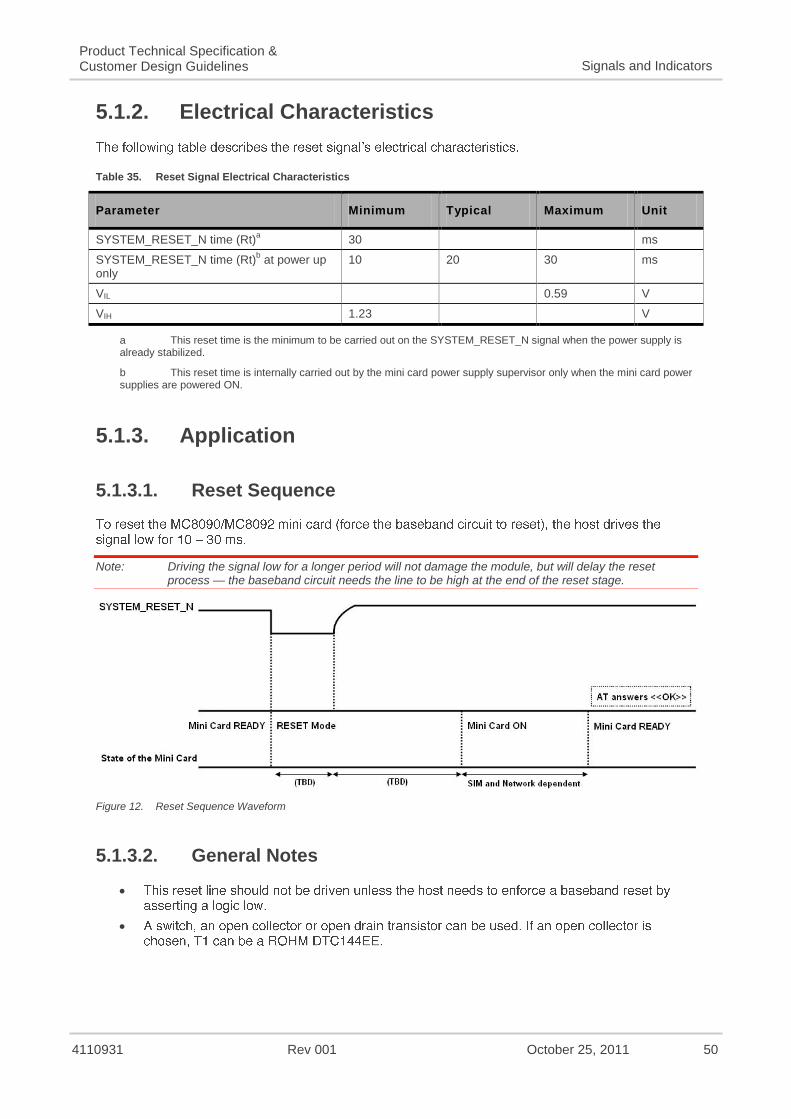
5.1.3.1. Reset Sequence
Note: Driving the signal low for a longer period will not damage the module, but will delay the reset process — the baseband circuit needs the line to be high at the end of the reset stage.
Figure 12. Reset Sequence Waveform
5.1.3.2. General Notes

4110931 Rev 001 October 25, 2011 51
Product Technical Specification & Customer Design Guidelines Signals and Indicators
Figure 13. Example of SYSTEM_RESET_N Pin Connection with Switch Configuration
Figure 14. Example of SYSTEM_RESET_N Pin Connection with Transistor Configuration
Table 36. Reset Settings
Reset Command SYSTEM_RESET_N (Pin 33) Operating Mode
1 0 Reset activated
0 1 Reset inactive
5.2. Wake Host Signal (WAKE_N)
Table 37. Wake Host Signal Features
Feature Details
Purpose Wake Host interface
Wake host when a predetermined condition is satisfied (for example, when a call is received).
Implementation Low = On
Active low, 1.8V logic
During the powered-off state, this pin may not be in a high impedance state. The host side must implement appropriate measures to accommodate this.
5.2.1. Pin Description
Table 38. Wake Signal Pin Description
Pin # Signal Name I/O I/O Type Description
32 WAKE_N* O Digital Wake Host interface
* This pin may be reconfigured for use in a full UART implementation. Refer to section 4.4.3 Full UART Implementation for more information.
4110931 Rev 001 October 25, 2011 52
Product Technical Specification & Customer Design Guidelines Signals and Indicators
5.2.2. Electrical Characteristics
Table 39. Wake Signal Electrical Characteristics
Parameter Minimum Typical Maximum Unit
Output High 1.25 1.80 1.90 V
Output Low 0 0.45 V
5.2.3. Application
Caution: This section is under review and subject to change.
5.3. Wireless Disable Signal (W_DISABLE_N)
Table 40. Wireless Disable Signal Features
Feature Details
Purpose Wireless disable
Used by host to disable or enable low power mode (‗airplane mode‘).
Implementation Low = Put module in airplane mode
Digital input
Active low, 1.8V logic
The MC8090/MC8092 has been provided with a 10 kΩ internal pull-up resistor (to module-provided 1.8 V reference (pin 11 — VREF_1V8)).
5.3.1. Pin Description
Table 41. Wireless Disable Signal Pin Description
Pin # Signal Name I/O I/O Type Description
20 W_DISABLE_N I Digital Wireless disable

4110931 Rev 001 October 25, 2011 53
Product Technical Specification & Customer Design Guidelines Signals and Indicators
5.3.2. Electrical Characteristics
Table 42. Wireless Disable Signal Electrical Characteristics
Parameter Minimum Typical Maximum Unit
Input High 1.23 1.80 2.00 V
Input Low -0.30 0.59 V
5.3.3. Application
Caution: This section is under review and subject to change.
5.3.3.1. Signal Timing
Figure 15. W_DISABLE_N Signal Timing
Table 43. W_DISABLE_N Signal Timing Parameters
Parameter Description
Period
Min Typ Max
t_WDIS_db W_DISABLE_N Debounce – Time between changing W_DISABLE_N logic level and RF mode changing.
1s - 7s

4110931 Rev 001 October 25, 2011 54
Product Technical Specification & Customer Design Guidelines
5.4. Flash LED (LED_FLASH)
Table 44. LED Signal Features
Feature Details
Purpose Flash LED output
Used by host to control LED status by controlling LED diode bias.
Implementation Open drain output.
Source / sink maximum — 8 mA
LED behavior can be configured by adjusting software settings.
LED pattern can be used to indicate network connection status.
Blink rate up to 10 Hz supported
5.4.1. Pin Description
Table 45. LED_FLASH Pin Description
Pin # Signal Name I/O I/O Type Reset State Description
42 LED_FLASH O Digital 1 and Undefined LED driving
5.4.2. Electrical Characteristics
Table 46. LED_FLASH Signal Electrical Characteristics
Parameter Condition Minimum Typical Maximum Unit
Tri-state
VOL 0.00 0.45 V

4110931 Rev 001 October 25, 2011 55
6. Power Consumption
Note: All specifications in these tables are preliminary, based on chipset published expectations.
Table 47. Averaged Standby DC Power Consumption (Preliminary/Estimated Values)
Signal Description Bands Typ. Peak Units Notes/Configuration
VCC
Standby current consumption with Sleep mode activated (assumes USB bus is fully suspended during measurements)
HSDPA / WCDMA
UMTS bands
2.3 778 mA DRX cycle = 8 (2.56 s)
GSM / GPRS / EDGE
GSM bands
3.2 678 mA MFRM = 5 (1.175 s)
Standby current consumption with Sleep mode deactivated (assumes USB bus is fully suspended during measurements)
HSDPA / WCDMA
UMTS bands
26.7 753 mA DRX cycle = 8 (2.56 s)
Module power up and idle (Assumes Sleep mode is never entered)
GSM / GPRS / EDGE
GSM bands
49.7 662 mA MFRM = 5 (1.175 s)
Module power up and idle (Assumes Sleep mode is never entered)
Low Power Mode (LPM) / Offline Mode
RF disabled, but module is operational
15.3 23.7 mA
State is entered when Watcher shuts down / turns off the radio.
LPM is the lowest possible (‗rock bottom‘) state in Sleep mode.
Table 48. Averaged Call Mode Data DC Power Consumption
Mode Current (at 3.6V) Tx (output) Power Conditions
WCDMA Data Current Consumption (includes USB bus current)
WCDMA Average
712 mA 23 dBm 384kbps*
247 mA 0 dBm
Peak 796 mA Averaged over 100µs
HSDPA Average
734 mA 23 dBm All speeds
263 mA 0 dBm
Peak 863 mA Averaged over 100µs
HSUPA Average
742 mA 23 dBm All speeds
271 mA 0 dBm
Peak 867 mA Averaged over 100µs
GSM / EDGE Data Current Consumption

4110931 Rev 001 October 25, 2011 56
Product Technical Specification & Customer Design Guidelines Power Consumption
Mode Current (at 3.6V) Tx (output) Power Conditions
GSM/GPRS
Average 283 mA (1TX)
468 mA (2TX) +33 dBm
50Ω
Max PCL for each band
Peak 2.24 A Averaged over 100µs
Worst case on 850 / 900 band
Average 94.2 mA (1TX)
117.3 mA (2TX) +10 dBm
50Ω
Peak 238.7 mA (TBD) Averaged over 100µs
Worst case on 850 / 900 band
EDGE
(850 MHz)
Average 206 mA (1TX)
302 mA (2TX)
396 mA (3TX)
482 mA (4TX)
+26 dBm 50Ω
Class 12
Peak 2.315 A +33 dBm
Averaged over 100µs
Worst case on 850 / 900 band
* Highest current is in Band I
Table 49. Miscellaneous DC Power Consumption (Preliminary Values)
Signal Description Band Typ. Max. Units Notes/Configuration
VCC
Module OFF leakage current
All bands 135 (TBD) µA Room temperature
USB transmit current All bands 10* (TBD) mA Full speed USB connection, CL = 50 pF on D+ and D- signals
* Typical value for MC8790 mini card used as estimate.
Table 50. Supported GPRS/EDGE Power Classes
Feature Notes
EGSM 900 / GSM 850 Power Class 4 2 W 33 dBm
GSM 1800 / 1900 Power Class 1 1 W 30 dBm
EDGE Power Class for 850 / 900 MHz Class E2*; 27 dBm, 0.5 W
EDGE Power Class for 800 / 1900 MHz Class E2*; 26 dBm, 0.4 W
* E2 power class applies to 8PSK modulation.

4110931 Rev 001 October 25, 2011 57
Product Technical Specification & Customer Design Guidelines Power Consumption
6.1. Power States
Table 51. Supported MC8090/MC8092 Power States
State Description Host Powered
Module Powered
USB Interface Active
RF Enabled
Normal
(Default state)
Capable of placing / receiving calls or establishing data connections on network
USB interface is fully active
Current consumption in a call or data connection is affected by:
Radio band in use
Tx power
Receive gain settings
Data rate
Number of active Tx time slots
Module defaults to Normal state when VCC is first applied in the absence of POWER_ON_N control.
Airplane Mode (RF off)
‗Airplane‘ mode — Rx / Tx are disabled; USB interface is active
State entered automatically when critical voltage / temperature thresholds are exceeded. Host should consider powering off module to prevent damage to unit.
Sleep (Idle Mode)
Normal state of module between calls or data connections.
Module cycles between wake (polling the network) and sleep, at network provider-determined interval.
Off
Host power is connected
Module is powered down (drawing minimal current from host power supply)
Disconnected
Host power is disconnected from module
All module-related voltages are at 0 V.

4110931 Rev 001 October 25, 2011 58
Product Technical Specification & Customer Design Guidelines Power Consumption
6.1.1. Power State Transitions
Table 52. Power State Transitions (including voltage/temperature trigger levels)
Transition
Voltage Temperature
Notes
Trigger V Trigger °C
Normal to Low Power
VOLT_HI_CRIT 4.4 TEMP_LO_CRIT -45 RF suspended
CNS_RADIO_POWER notification issued*
VOLT_LO_CRIT 3.0 TEMP_HI_CRIT 110
Low Power to Normal
VOLT_HI_NORM 4.3 TEMP_NORM_LO -40
RF suspended
CNS_RADIO_POWER notification issued*
Low Power to Normal
or
Remain in Normal (remove warnings)
VOLT_LO_NORM 3.6 TEMP_HI_NORM 85
Normal (issue warning)
VOLT_LO_WARN 3.3 TEMP_HI_WARN 95
* Notification issued only if previously enabled. Refer to document [6] AirPrime UMTS MC Series CnS Reference for details.
Figure 16. Automatic (“Triggered”) Power State Transitions

4110931 Rev 001 October 25, 2011 59
7. Network Technology Specifications
7.1. UMTS WCDMA FDD Specifications
Table 53. Supported WCDMA FDD Specifications
Specification Supported Feature
Physical Layer Specification
DL Channels: BCH, PCH, FACH, DCH, AICH, CPICH
UL Channels: RACH, DCH
Measurement for PCCPCH RSCP RSCP/SIR
BTFD
CCTrCH
As defined by examples in 25.944
Multifinger support
Cell reselection
Soft handover
Power control
PICH / DRX
Measurement for SFN / CFN timing, SFN / SFN timing
Cell selection
RLC Specifications
TM / UM / AM
Max AM entities (4)
3 for signalling
1 for user data
Only timer based polling for AM
No timer based SDU discard for TM / UM / AM
Poll PU polling for AM
Poll prohibit
Polling options: Last ReTX PU Poll, Poll Window, Poll SDU
Status report transfer: Timer Status, Status Prohibit, Missing PU indicator
Reset procedure: Indication to RRC
Suspend / Resume
Timer based SDU discard (UM / AM / TM)
Status report transfer: Piggybacked Status PDUs, EPC based transfer
SUFIs: Sending BITMAP and RLIST
Start / stop for all three modes
RRC Specifications
Cell selection
RRC connection establishment
RRC connection release
System information processing
Idle mode paging
Dedicated mode paging

4110931 Rev 001 October 25, 2011 60
Product Technical Specification & Customer Design Guidelines Network Technology Specifications
Specification Supported Feature
Initial direct transfer
Uplink direct transfer
Downlink direct transfer
Signalling connection release
Signalling connection release request
Radio bearer establishment
Radio bearer release
Cell update
UE capability enquiry
Transmission of UE capability
Cell reselection
Measurement control
Measurement reporting
Soft HO/Active Set update
DRX mode
NV support for RRC channel scan
Radio bearer reconfiguration
Transport channel reconfiguration
Physical channel reconfiguration
UTRAN mobility information
Integrity protection
Security mode control
Encryption: UEA1
Integrity algorithm: U1A11
7.2. Supported Specifications
Table 54. Supported Specifications
Item Comments
8PSK modulation Octagonal Phase Shift Keying
Coding schemes MCS1-4 are GMSK and MCS5-9 are 8PSK.
GPRS header compression Data packet header compression supported

4110931 Rev 001 October 25, 2011 61
Product Technical Specification & Customer Design Guidelines Network Technology Specifications
Item Comments
3GPP compliance
Protocol stack supports the requirements of:
GPRS/EDGE: 3GPP Release 99 and GERAN Feature Package #1
WCDMA: Release 6
GPRS operation mode class B Class B terminals support either circuit-switched or packet-switched traffic (with simultaneous network attachment) but do not support both kinds of traffic simultaneously.
Link Adaptation (LA) Together with IR (next table entry), LA adapts the EGPRS transmission to meet changing radio link conditions.
EGPRS Incremental Redundancy (IR)
IR adjusts the physical layer code rate to actual channel conditions by incrementally transmitting redundant information until decoding is successful.
Automatic Repeat Request (ARQ) protocol takes care of requesting and retransmitting incorrectly received blocks. ARQ enables both dynamic RLC window management (to avoid window stalling) and dynamic RLC polling frequency (to minimize retransmission delay and save radio bandwidth).
GPRS multislot class 10 Multislot class 10 and 12 allow for dynamic allocation of time slots.
EGPRS multislot class 12
NC0 NC0 is the normal mode of control for a GPRS mobile in which the MS (Mobile Station) performs autonomous cell reselection.
DPC
Downlink Power Control
Allows the network to adjust the downlink power of any dedicated channels on the BTS based on measurement reports sent by the mobile. This allows the network to reduce interference between multiple mobiles while still maintaining adequate signal quality for the individual mobiles.
One-phase packet access for GPRS In establishing a TBF (Temporary Block Flow) connection, the MS (Mobile
Station) requests either one-phase or two-phase packet access.
In one-phase access, the network responds to a packet channel request by sending a packet uplink assignment message and reserving resources for uplink transfer of a number of radio blocks.
In two-phase access, a packet resource request is sent on receipt of the packet uplink assignment.
One-phase packet access for EGPRS
Two-phase packet access for GPRS
Two-phase packet access for EGPRS
RLC-acknowledged operation mode The RLC-acknowledged and LLC-acknowledged modes are used to ensure
the integrity of received data where QoS requires it. RLC (Radio Link Control) acknowledgment is typically the default (depending on the network and user profile). LLC-acknowledgment is optional and ensures that all LLC (Logical Link Control) frames are received without error. Since LLC-acknowledged mode requires acknowledgement of all LLC frames, the mode has an impact on throughput.
RLC-unacknowledged operation mode
LLC-acknowledged transmission mode
LLC-unacknowledged transmission mode
GSM network operation mode I and II
The Network Operating Mode specifies the coordination of paging for circuit-switched and packet-switched services.
Mode I - The mobile can receive circuit-switched pages while in a packet-switched call.
Mode II - The mobile cannot receive a circuit-switched page while in a packet-switched call, as it would force the mobile to constantly monitor its CCCH channel.
PBCCH / PCCCHI
Packet Broadcast Control Channel
PBCCH is a packet data signalling channel that can supplement the BCCH GSM control channel, allowing decoupling of voice and packet control channels to set up data calls. PBCCH broadcasts GPRS / EGPRS specific cell re-selection parameters for serving and neighbour cells used in cell selection / re-selection for packet services.
4110931 Rev 001 October 25, 2011 62
Product Technical Specification & Customer Design Guidelines Network Technology Specifications
Item Comments
GPRS test modes (ETSI test mode A and B)
The European Telecommunications Standards Institute (ETSI) defines standards and requirements for testing of GSM mobile equipment.
In test mode A, the mobile requests an uplink TBF and transmits random data on a designated number of timeslots. This causes a device to transmit data without using upper layer protocols. Once the transmission has started, the downlink TBF halts. The device remains in this mode until the testing equipment terminates it.
In test mode B, the mobile is prompted to receive data on a number of specified downlink timeslots and re-transmit the same data back on the corresponding uplink timeslots. Test mode B allows tests to be performed on both the transmitter and receiver within a single session.
NACC (R4 GERAN Feature Set 1)
Network Assisted Cell Change
Enables the network to provide additional information about neighbour cells to the mobile while in a packet data session, which decreases the experienced service delays caused by cell re-selection.
MAIO
Mobile Allocation Index Offset
MAIO and Hopping Sequence Number (HSN) are used in conjunction with Frequency Hopping to determine the hopping sequence used in each frame. The MAIO supports as many values as there are frequencies in the hopping list, and these are used to indicate the offset within the hopping list that identifies the frequency used.
Packet enhanced measurement report (PEMR)
Packet Enhanced Measurement Report (PEMR) is one of the RLC / MAC (Radio Link Control and Medium Access Control) control messages that include a carrier identifier. This message is a requirement of supporting multicarrier TBF.
Delayed TBF Release
Delayed Temporary Block Flow Release (also called Extended Uplink TBF)
Delayed TBF Release reduces latency between uplink data transfers and reduced signalling on the network by maintaining a connection for brief periods when the network is temporarily inactive and the mobile station has no radio link control information to send. For this feature to work properly, the mobile station must support delayed TBF release.
Extended Dynamic Allocation Radio blocks can be transmitted on up to four different PDCHs. Permits full class 12 operation.
Single Antenna Interference Cancellation (SAIC)
SAIC mitigates code-channel interference from neighbouring cells resulting in fewer dropped calls, and faster download rates for e-mail and websites.
Circuit-switched data bearers
These circuit-switched data bearers are supported on 2G networks:
Asynchronous 9,600 bps
Asynchronous 14,400 bps
Security
Encryption support GPRS / EGPRS support GEA1, GEA2, and GEA3 data ciphering.
GSM CSD and SMS use A5/1 and A5/3 encryption.
PAP for RADIUS authentication - GPRS / EGPRS
PAP (Password Authentication Protocol) is a method of authenticating usernames and passwords against a database on a RADIUS (Remote Authentication Dial-In User Service) server. In a standard login, the service provider prompts for a username and password. In PAP authentication, the username and password are entered in the client's dialling software and sent as one data package, rather than the server sending a login prompt and waiting for a response.
CHAP for RADIUS authentication - GPRS / EGPRS
CHAP (Challenge Handshake Authentication Protocol) is a more secure method for connecting to a system than PAP. After a link is established, the server sends a challenge message to the client. The client responds with a value calculated using a one-way hash function. The server compares its own calculation of the expected hash value to the client's response. If the values match, the authentication is acknowledged; otherwise the connection is terminated.

4110931 Rev 001 October 25, 2011 63
Product Technical Specification & Customer Design Guidelines Network Technology Specifications
Item Comments
Support for encryption algorithm UEA1 (Kasumi)
UEA1 (UMTS Encryption Algorithm) generates the keystream as a function of a cipher key that is re-synchronized to every MAC / RLC frame. UEA is based on the Kasumi algorithm.
Support for integrity algorithm UIA1 (Kasumi)
UIA1 (UMTS Integrity Algorithm) is the algorithm used to compute the IK (Integrity Key) used in message authentication. UIA is based on the Kasumi algorithm.
UMTS
WCDMA-to-GPRS reselection in CELL_FACH CELL_FACH is an RRC (Radio Resource Control) service state in which cell
reselection is performed. This feature prevents dropping of RRC connections. Inter-frequency reselection in
Cell_FACH
Radio link failure
Radio link failure is a procedure that indicates an ‗out-of-synch‘ state on one or more radio links. Node B of the RNC (Radio Network Controller) reports this event before attempting resynchronization. The radio link restoration procedure indicates restoration of the ‗synchronized‘ state.
SIB scheduling SIB (System Information Block) scheduling controls the broadcasting of information to user equipment in a cell. The user equipment retrieves the schedule, and is then able to change to sleep mode, receiving only those blocks that it needs.
SIB modification
Re-establishment procedure Following a radio link failure, the RNC maintains the RRC connection, waiting for re-establishment.
VT + PS call (subject to network availability)
Simultaneous VT (Video Terminal) and PS (Packet Switched) calls are supported.
Packet Cell Change Order from
GSMUTRAN Call transfer between GSM-based and UTRAN-based cells is supported.
Background PLMN search Improved algorithm for Higher Priority PLMN (HPPLMN) search while camped on a 3G cell.
Configurable Release 5 or Release 99 support
Circuit-switched data bearers
Data bearers
These circuit-switched data bearers are supported on 3G networks:
Synchronous transparent mode = 64000 bps
Synchronous transparent mode = 56000 bps
Asynchronous V110 UDI = 14400 bps
Asynchronous V110 UDI = 28800 bps
Asynchronous V110 UDI = 38400 bps
Asynchronous V120 = 14400 bps
Asynchronous V120 = 28800 bps
Asynchronous V120 = 56000 bps
HSDPA
Data rates The following data rates are supported:
Category 10 (14.4 Mbps)
HSDPA logical channels
These HSDPA logical channels are supported:
HS-SCCH
HS-DPCCH
HS-PDSCH—Up to ten HS-PDSCH channels are supported.

4110931 Rev 001 October 25, 2011 64
Product Technical Specification & Customer Design Guidelines Network Technology Specifications
Item Comments
HSDPA transport channels
HS-DSCH is supported at these rates:
120 kbps
240 kbps
360 kbps
Incremental redundancy
IR adjusts the physical layer code rate to actual channel conditions by incrementally transmitting redundant information until decoding is successful. Automatic Repeat Request (ARQ) protocol takes care of requesting and retransmitting incorrectly received blocks. ARQ enables both dynamic RLC window management (to avoid window stalling) and dynamic RLC polling frequency (to minimize retransmission delay and save radio bandwidth).
Chase combining retransmission scheme
The Chase combining retransmission scheme is the simplest HARQ (Hybrid Automatic Request) link adaptation technique. HARQ techniques are used to enhance system performance.
HSDPA Compressed Mode Allows the user equipment to interrupt transmission and reception during a call for brief periods in order to measure the signal strength of neighbouring cells that use different frequencies.
(MC8090)
Concurrent voice and HSDPA data
(TBD)
HSDPA Indicator Allows user interface to display an indicator when HSDPA data transfer is in progress.
Receiver equalizer support
Miscellaneous
Fast link adaptation The data rate is adapted to radio conditions.
Vary the effective code rate The effective code rate is varied based on code space resources.
HARQ, MAC-HS disassembly
MAC-HS (High Speed MAC) is the base station MAC (Medium Access Control) protocol. MAC-HS enables fast radio resource allocation.
MAC-HS reordering queue distribution and processing support
Cell change
These cell change methods are supported:
Synchronous and non-synchronous
Intra-Node B (softer repointing)
Inter-Node B (soft repointing)
Up-switching and down-switching of PS RAB between HS-PDSCH and DPCH
RAB (Radio Access Bearer) and channel mappings between the HS-PDSCH (High Speed Physical Downlink Shared Channel) and DPCH (Dedicated Physical Channel) are reallocated according to volume thresholds and inactivity timers.
Ciphering on the HS channel Ciphering on high-speed channels protects radio-transmitted data against unauthorized third parties.
Support to not resume the HS channel if inter-RAT handover fails, but save the RB mapping information
RB (Radio Bearer) mapping information is preserved if a high-speed channel is dropped due to the failure of an inter-RAT (Radio Access Technology) transfer.
Support to not resume the HS channel if a radio link failure occurs, but save the RB mapping information
RB (Radio Bearer) mapping information is preserved if a high-speed channel is dropped due to a radio link failure.
WINS address support primary and secondary
Primary and secondary IP addresses can be assigned for WINS (Windows Internet Name Service) name servers.
(MC8090/MC8092 with PCM)
Voice support Digital audio (PCM) is supported.

4110931 Rev 001 October 25, 2011 65
Product Technical Specification & Customer Design Guidelines Network Technology Specifications
Item Comments
Unstructured supplementary services data (USSD)
USSD provides support for transmitting information over the GSM network signalling channels. It provides fast session-based communication between the user and an application, enabling use of text messaging, prepaid roaming, chat, etc.
Supplementary services Support for supplementary voice services such as Call Hold, Call Forward, Call Waiting, Multi-party Calls, Caller ID, Fixed Number Dialling, Service Dialling Numbers, etc.
Cell reselection / handover Supports InterRat and InterFrequency cell-reselection and handover between supported frequency bands.
Security - IMEI Security
SIM lock The device can be ‗MEP locked‘ to a particular PLMN.
SIM security Both CHV1 and CHV2 are supported (unlock and unblock).
7.3. UMTS (WCDMA)/GSM Specifications
Table 55. UMTS (WCDMA)/GSM Specifications
Item GSM UMTS
Mobility management
Automatic PLMN selection / reselection
Location updating procedure
IMSI attach procedure
IMSI detach procedure
Periodic location update
Authentication procedure
CM connection establishment from MS or network
CM connection release
Encryption key management
TMSI reallocation
Paging response
Abort procedure
Identification
CN system information
Call re-establishment
MM connection establishment emergency calls
Inter-RAT change procedure
CS follow-on procedure
Access class barring
Resumption procedure for Class B operation in GPRS
Handling of domain change CS to CS/PS and other combinations
MM information
Network mode of operation I, II

4110931 Rev 001 October 25, 2011 66
Product Technical Specification & Customer Design Guidelines Network Technology Specifications
Item GSM UMTS
GPRS mobility management
GPRS attach
GPRS detach
Routing area update
GPRS authentication
GPRS identification
GMM status
Periodic routing area update
Ciphering
Access class barring
GMM status
Combined GPRS attach
Combined GPRS detach
Combined routing location / area update
PS SMS
Network initiated combined GPRS detach
Network mode of operation change
RAB management
QoS-based activation, network offers lower / higher QoS
Primary PDP context activation
PDP context deactivation
Data services
AT commands
MS PS data calls
Single PDP context
PDP type PPP
PDP type IP
9.6 / 14.4 CS transparent data N/A
9.6 / 14.4 CS nontransparent data N/A
Fax
MT Sync CS data calls
MO Sync CS data calls
V.80 N/A
V.42bis N/A
Multiple PDP context profiles (up to 16)
SMS specifications
CS domain MT SMS point-to-point
CS domain MO SMS point-to-point
SMMA
Dedicated mode
Message classes 0, 1, 2, 3, none
SMS / SMSP / SMSS access from SIM / USIM
Reply path

4110931 Rev 001 October 25, 2011 67
Product Technical Specification & Customer Design Guidelines Network Technology Specifications
Item GSM UMTS
Validity period
PS domain MT SMS point-to-point
PS domain MO SMS point-to-point
SMS status reports
SMS commands

4110931 Rev 001 October 25, 2011 68
8. Reliability Compliance and Recommended Standards
8.1. Reliability Compliance
Table 56. Standards Conformity for the AirPrime MC8090/MC8092 Mini Card
Abbreviation Definition
IEC International Electro technical Commission
ISO International Organization for Standardization
8.2. Applicable Standards
Note: References to any features can be found from these standards.
Table 57. Applicable Standards and Requirements
DocumentCurrent Version
Title
IEC6006826 7.0 Environmental testing - Part 2.6: Test FC: Sinusoidal Vibration.
IEC60068234 73
Basic environmental testing procedures part 2: Test FD: random vibration wide band - general requirements
Cancelled and replaced by IEC60068-2-64. For reference only.
IEC60068264 2.0Environmental testing - part 2-64: Test FH: vibration, broadband random and guidance.
IEC60068232 2.0Basic environmental testing procedures - part 2: Test ED: (procedure 1) (withdrawn & replaced by IEC60068-2-31).
IEC60068231 2.0 Environmental testing part 2-31: Test EC: rough handling shocks, primarily for equipment-type specimens.
IEC60068229 2.0
Basic environmental testing procedures - part 2: Test EB and guidance: bump
Withdrawn and replaced by IEC60068-2-27. For reference only.
IEC60068227 4.0 Environmental testing - part 2-27: Test EA and guidance: shock.
IEC60068214 6.0 Environmental testing - part 2-14: Test N: change of temperature.
IEC6006822 5.0 Environmental testing - part 2-2: Test B: dry heat.
IEC6006821 6.0 Environmental testing - part 2-1: Test A: cold.
IEC60068230 3.0 Environmental testing - part 2-30: Test DB: damp heat, cyclic (12 h + 12 h cycle).
IEC6006823 69 w/A1
Basic environmental testing procedures part 2: Test CA: damp heat, steady State
Withdrawn and replaced by IEC60068-2-78. For reference only.
IEC60068278 1.0 Environmental testing part 2-78: Test CAB: damp heat, steady state.

4110931 Rev 001 October 25, 2011 69
Product Technical Specification & Customer Design Guidelines
Reliability Compliance and Recommended Standards
DocumentCurrent Version
Title
IEC60068238 2.0 Environmental testing - part 2-38: Test Z/AD: composite temperature/humidity cyclic test.
IEC60068240 1.0 w/A1 Basic environmental testing procedures - part 2: Test Z/AM combined cold/low air pressure tests.
ISO167501 2ND Road vehicles - environmental conditions and testing for electrical and electronic equipment - part 1: general.
ISO167502 2ND Road vehicles - environmental conditions and testing for electrical and electronic equipment - part 2: electrical loads.
ISO167503 2ND Road vehicles - environmental conditions and testing for electrical and electronic equipment - part 3: mechanical loads.
ISO167504 2ND Road vehicles - environmental conditions and testing for electrical and electronic equipment - part 4: climatic loads.
IEC60529 2.1 w/COR2 Degrees of protection provided by enclosures (IP code).
IEC60068217 4.0 Basic environmental testing procedures - part 2: Test Q: sealing.
IEC60068218 2.0 Environmental testing - part 2-18: Tests - R and guidance: water.
IEC60068270 1.0 Environmental testing - part 2: tests - test XB: abrasion of markings and letterings caused by rubbing of fingers and hands.
IEC60068268 1.0 Environmental testing - part 2: tests - test l: dust and sand.
IEC60068211 3.0 Basic environmental testing procedures, part 2: test KA: salt mist.
IEC60068260 2.0 Environmental testing - part 2: Test KE: flowing mixed gas corrosion test.
IEC60068252 2.0 w/COR Environmental testing - part 2: Test KB: salt mist, cyclic (sodium chloride solution).
8.3. Environmental Specifications
Table 58. Operating Class Temperature Range
Conditions Temperature Range
Operating/Class A -30°C to +70°C
Operating/Class B -40°C to +85°C
Storage -40 °C to +85°C

4110931 Rev 001 October 25, 2011 70
Product Technical Specification & Customer Design Guidelines
Reliability Compliance and Recommended Standards
8.3.1. Function Status Classification
Note: The word “function” as used here concerns only the function performed by the MC8090/MC8092 mini card.
Table 59. ISO Failure Mode Severity Classification
Class Description
Class AThe MC8090/MC8092 mini card remains fully functional during and after environmental exposure; and shall meet the minimum requirements of 3GPP or appropriate wireless standards.
Class B
The MC8090/MC8092 mini card remains fully functional during and after environmental exposure; and shall exhibit the ability to establish a voice, SMS or DATA call at all times even when one or more environmental constraint exceeds the specified tolerance. Unless otherwise stated, full performance should return to normal after the excessive constraint(s) have been removed.
8.4. Reliability Prediction Model
8.4.1. Life Stress Test
Table 60. Life Stress Test
Designation Condition
Performance Test PT3T° & PT
Standard: N/A
Special conditions:
Temperature:
Class A: -30°C to +70°C
Class B: -40°C to +85°C
Rate of temperature change: ± 3°C/min
Recovery time: 3 hours
Operating conditions: Powered
Duration: 14 days

4110931 Rev 001 October 25, 2011 71
Product Technical Specification & Customer Design Guidelines
Reliability Compliance and Recommended Standards
8.4.2. Environmental Resistance Stress Tests
Table 61. Environmental Resistance Stress Tests
Designation Condition
Cold Test Active
COTA
Standard: IEC 680068-2-1, Test Ad
Special conditions:
Temperature:
Rate of temperature change: dT/dt >= ± 3°C/min
Recovery time: 3 hours
Operating conditions: Powered
Duration: 72 hours
Cold Test Active
COTP
Standard: IEC 680068-2-1, Test Ab
Special conditions:
Temperature: -40°C
Rate of temperature change: dT/dt >= ± 3°C/min
Recovery time: 3 hours
Operating conditions: Un-powered
Duration: 72 hours
Resistance to Heat Test
RH
Standard: IEC 680068-2-2, Test Bb
Special conditions:
Temperature: +85°C
Rate of temperature change: dT/dt >= ± 3°C/min
Recovery time: 3 hours
Operating conditions: The DUT is switched ON for 1 min and then OFF for 1 min
Duration: 50 days
Dry Heat Test
DHT
Standard: IEC 680068-2-2, Test Bb
Special conditions:
Temperature: +85°C
Rate of temperature change: dT/dt >= ± 3°C/min
Recovery time: 3 hours
Operating conditions: Un-powered
Duration: 72 hours
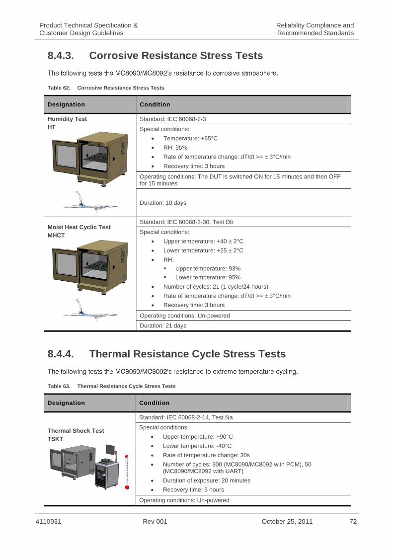
4110931 Rev 001 October 25, 2011 72
Product Technical Specification & Customer Design Guidelines
Reliability Compliance and Recommended Standards
8.4.3. Corrosive Resistance Stress Tests
Table 62. Corrosive Resistance Stress Tests
Designation Condition
Humidity Test
HT
Standard: IEC 60068-2-3
Special conditions:
Temperature: +65°C
RH:
Rate of temperature change: dT/dt >= ± 3°C/min
Recovery time: 3 hours
Operating conditions: The DUT is switched ON for 15 minutes and then OFF for 15 minutes
Duration: 10 days
Moist Heat Cyclic Test
MHCT
Standard: IEC 60068-2-30, Test Db
Special conditions:
Upper temperature: +40 ± 2°C
Lower temperature: +25 ± 2°C
RH:
Upper temperature: 93%
Lower temperature: 95%
Number of cycles: 21 (1 cycle/24 hours)
Rate of temperature change: dT/dt >= ± 3°C/min
Recovery time: 3 hours
Operating conditions: Un-powered
Duration: 21 days
8.4.4. Thermal Resistance Cycle Stress Tests
Table 63. Thermal Resistance Cycle Stress Tests
Designation Condition
Thermal Shock Test
TSKT
Standard: IEC 60068-2-14, Test Na
Special conditions:
Upper temperature: +90°C
Lower temperature: -40°C
Rate of temperature change: 30s
Number of cycles: 300 (MC8090/MC8092 with PCM), 50 (MC8090/MC8092 with UART)
Duration of exposure: 20 minutes
Recovery time: 3 hours
Operating conditions: Un-powered

4110931 Rev 001 October 25, 2011 73
Product Technical Specification & Customer Design Guidelines
Reliability Compliance and Recommended Standards
Designation Condition
Duration: 8 days
Temperature Change
TCH
Standard: IEC 60068-2-14, Test Nb
Special conditions:
Upper temperature: +90°C
Lower temperature: -40°C
Rate of temperature change: dT/dt >= ± 3°C/min
Number of cycles: 400
Duration of exposure: 10 minutes
Recovery time: 3 hours
Operating conditions: Un-powered
Duration: 30 days
8.4.5. Mechanical Resistance Stress Tests
Table 64. Mechanical Resistance Stress Tests
Designation Condition
Sinusoidal Vibration Test SVT
Standard: IEC 60068-2-6, Test Fc
Special conditions:
Frequency range Hz to 000Hz
Displacement: 0.35mm (peak)
Frequency range: Hz to 62Hz
Acceleration: 5G
Frequency range: 62Hz to 200Hz
Acceleration: 3G
Frequency range: 200Hz 00Hz
Acceleration: 1G
Sweep rate: 1 octave/min
Test duration
Sweep directions: X, Y and Z
Operating conditions: Un-powered
Duration: 72 hours
Random Vibration Test
RVT
Standard: IEC 60068-2-64
Special conditions:
Density m /s3
Frequency range
0.1 g2/Hz at 10Hz
0.01 g2/Hz at 250Hz
0.0005 g2/Hz at 1000Hz
0.0005 g2/Hz at 2000Hz
Slope: -3dB/octave
Acceleration: 0.9gRMS
Number of axis: 3

4110931 Rev 001 October 25, 2011 74
Product Technical Specification & Customer Design Guidelines
Reliability Compliance and Recommended Standards
Designation Condition
Operating conditions: Un-powered
Duration: 24 hours
Mechanical Shock Test
MST
Standard: IEC 60068-2-27, Test Ea
Special conditions:
Shock Test 1:
Wave form: Half sine
Peak acceleration: 30G
Duration: 11ms
Number of shocks: 8 per direction
Number of directions: 6 (±X, ±Y, ±Z)
Shock Test 2:
Wave form: Half sine
Peak acceleration: 100G
Duration: 6ms
Number of shocks: 3 per direction
Number of directions: 6 (±X, ±Y, ±Z)
Operating conditions: Un-powered
Duration: 72 hours
8.4.6. Handling Resistance Stress Tests
Table 65. Handling Resistance Stress Tests
Designation Condition
ESD Test
Standard: IEC 1000-4-2
Special conditions:
Contact and Air discharges: 10 positive and 10 negative applied
Contact Voltage:
Air Voltage : 2kV,
Operating conditions: Powered
Duration: 24 hours
Free Fall Test
FFT 1
Standard : IEC 60068-2-32, Test Ed
Special conditions:
Drop: 2 samples for each direction
Equivalent drop height: 1m
Number of directions: 6 (±X, ±Y, ±Z)
Number of drops/face: 2
Operating conditions: Un-powered
Duration: 24 hours
Free Fall Test Standard : Standard Sierra Wireless Methodology

4110931 Rev 001 October 25, 2011 75
Product Technical Specification & Customer Design Guidelines
Reliability Compliance and Recommended Standards
Designation Condition
FFT 2
Special conditions:
Drop: 2 samples for each direction
Equivalent drop height: 1.5m
Number of directions: 6 (±X, ±Y, ±Z)
Number of
DUT in end-user host device
Operating conditions: Un-powered
Duration: 24 hours
4110931 Rev 001 October 25, 2011 76
9. Design Guidelines
9.1. SIM Interface Routing Constraint
9.2. EMC and ESD Recommendations
Note: The AirPrime MC8090/MC8092 mini card does not include any protection against over voltage.
Note: The level of protection required depends on your application.

4110931 Rev 001 October 25, 2011 77
Product Technical Specification & Customer Design Guidelines Design Guidelines
Table 66. ESD Specifications
Connection Specification
Operational The RF port (antenna launch and RF connector) complies with the following standard:
IEC 61000-4-2 Electrostatic Discharge Immunity:
Test: Level3
Contact Discharge: ±6 kV
Air Discharge: ±8 kV
Non-operational The host connector Interface complies with the following standards only:
±1 kV Human Body Model (JESD22-A114-B)
±125 V Charged Device Model (JESD22-C101)
9.3. Mechanical Integration
Note: Attention should be paid to antenna cable integration (bending, length, position, etc).
9.4. Operating System Upgrade
Tip: In order to follow regular changes in the GPRS standard and to offer a state-of-the-art operating system, Sierra Wireless recommends that the application designed around a mini card (or mini card based product) should allow easy operating system upgrades on the mini card via the recommended firmware download protocol (see document [7] AirCard/AirPrime USB Driver Developer’s Guide). Therefore, the application shall either allow a direct access to the mini card serial interface through an external connector or implement any mechanism allowing the mini card operating system to be downloaded.

4110931 Rev 001 October 25, 2011 78
10. Embedded Testability
10.1. Testing Assistance Provided by Sierra Wireless
10.2. Integration Requirements
10.3. IOT/Operator
10.4. Module Testing Recommendations
–

4110931 Rev 001 October 25, 2011 79
Product Technical Specification & Customer Design Guidelines Embedded Testability
Figure 17. Recommended Thermocouple Location
Note: Make sure that your system design provides sufficient cooling for the module. The RF shield temperature should be kept below 90°C when integrated to prevent damaging the module’s components.
10.5. Serial Link Access
10.6. RF Output Accessibility

4110931 Rev 001 October 25, 2011 80
11. Certification Compliance and Recommended Standards
11.1. UMTS Compliance Acceptance and Certification
Note: Tests that require features not supported by the MC8090/MC8092 (as defined by this document) are not supported.
11.2. Certification Compliance
Table 67. Standards Conformity for the MC8090/MC8092 Mini Card
Domain Applicable Standard MC8090 MC8092
Safety standard EN 60950-1 (ed.2006)
Health standard (EMF Exposure Evaluation)
EN 62311 (ed. 2008)
Efficient use of the radio frequency spectrum
EN 301 511 (V 9.0.2)
EMC EN 301 489-1 (v1.8.1)
EN 301 489-7 (v1.3.1)
FCC FCC Part 22, 24
IC RSS-132 Issue 2
RSS-133 Issue 5
EU
FTA GCF regulatory certification
CE Mark regulatory certification of compliance
Interoperability Testing (IOT)
CE CE
A-Tick certification
North / Latin America operators / carriers
PTCRB approval per NAPRD requirement
AT&T

4110931 Rev 001 October 25, 2011 81
Product Technical Specification & Customer Design Guidelines
Certification Compliance and Recommended Standards
11.3. Applicable Standards
11.3.1. Important Notice
11.3.2. Safety and Hazards

4110931 Rev 001 October 25, 2011 82
Product Technical Specification & Customer Design Guidelines
Certification Compliance and Recommended Standards
11.3.3. Important Compliance Information for North American Users
Note: If this mini card is intended for use in a portable device, you are responsible for separate approval to satisfy the SAR requirements of FCC Part 2.1093 and IC RSS-102.
11.3.4. EU Regulatory Conformity

4110931 Rev 001 October 25, 2011 83
12. Customization
Table 68. Customizable Features
Name Description Default
MEP network locked Mobile Equipment Personalization network locked to only allow use with specific preconfigured PLMNs (SIMs). MMI supports the entry of an unlock code subject to permanent locking feature below.
Off
MEP service provider locked
Permanent MEP locked Can block deactivation of MEP locked feature Off
Roaming indicator disable*
Watcher never shows the onscreen roaming indicator.
Indicator enabled
SIM PUK prompt enable If enabled, Watcher shows the message "SIM blocked please enter PIN code".
Disabled, Watcher displays "Contact Service Provider" when SIM PIN is blocked
Scan for profile The modem scans through all its programmed profiles to find successful GPRS connection.
Not scanning. Only the selected profile is used for connection.
Display of IMSI Display of International Mobile Subscriber Identity via AT+CIMI command
Display enabled
UART baudrate Default UART speed 115200 bps
UART enabled Defines whether UART port is enabled by default or not
UART enabled
* Only available if supported in the user interface.

4110931 Rev 001 October 25, 2011 84
13. Signal Reference Schematics
Figure 18. USB Interface
Figure 19. SIM Interface

4110931 Rev 001 October 25, 2011 85
14. References
14.1. Web Site Support
14.2. Reference Documents
14.2.1. Sierra Wireless Documentation
14.2.2. Industry/ Other Documentation

4110931 Rev 001 October 25, 2011 86
Product Technical Specification & Customer Design Guidelines References
14.3. List of Abbreviations
Abbreviation Definition
AC Alternative Current
ADC Analog to Digital Converter
A/D Analog to Digital conversion
AF Audio-Frequency
AT Attention (prefix for modem commands)
AUX Auxiliary
CAN Controller Area Network
CB Cell Broadcast
CEP Circular Error Probable
CLK Clock
CMOS Complementary Metal Oxide Semiconductor
CS Coding Scheme
CTS Clear To Send
DAC Digital to Analogue Converter
dB Decibel
DC Direct Current
DCD Data Carrier Detect
DCE Data Communication Equipment
DCS Digital Cellular System
DR Dynamic Range
DSR Data Set Ready
DTE Data Terminal Equipment
DTR Data Terminal Ready
EDGE Enhance Data rates for GSM Evolution
EFR Enhanced Full Rate
E-GSM Extended GSM
EGPRS Enhance GPRS
EMC Electromagnetic Compatibility
EMI Electromagnetic Interference
EMS Enhanced Message Service
EN Enable
ESD Electrostatic Discharges
FIFO First In First Out
FR Full Rate
FTA Full Type Approval
GND Ground
GPI General Purpose Input
GPC General Purpose Connector
GPIO General Purpose Input Output
GPO General Purpose Output
GPRS General Packet Radio Service

4110931 Rev 001 October 25, 2011 87
Product Technical Specification & Customer Design Guidelines References
Abbreviation Definition
GPS Global Positioning System
GSM Global System for Mobile communications
HR Half Rate
I/O Input / Output
LED Light Emitting Diode
LGA Land Grid Array
LNA Low Noise Amplifier
MAX Maximum
MIC Microphone
MIN Minimum
MMS MultiMedia Message Service
MO Mobile Originated
MT Mobile Terminated
na Not Applicable
NC Not Connected
NF Noise Factor
NMEA National Marine Electronics Association
NOM Nominal
NTC Negative Temperature Coefficient
PA Power Amplifier
Pa Pascal (for speaker sound pressure measurements)
PBCCH Packet Broadcast Control Channel
PC Personal Computer
PCB Printed Circuit Board
PDA Personal Digital Assistant
PFM Power Frequency Modulation
PSM Phase Shift Modulation
PWM Pulse Width Modulation
RAM Random Access Memory
RF Radio Frequency
RFI Radio Frequency Interference
RHCP Right Hand Circular Polarization
RI Ring Indicator
RST Reset
RTC Real Time Clock
RTCM Radio Technical Commission for Maritime services
RTS Request To Send
RX Receive
SCL Serial Clock
SDA Serial Data
SIM Subscriber Identification Module
SMS Short Message Service
SPI Serial Peripheral Interface

4110931 Rev 001 October 25, 2011 88
Product Technical Specification & Customer Design Guidelines References
Abbreviation Definition
SPL Sound Pressure Level
SPK Speaker
SRAM Static RAM
TBC To Be Confirmed
TDMA Time Division Multiple Access
TP Test Point
TVS Transient Voltage Suppressor
TX Transmit
TYP Typical
UART Universal Asynchronous Receiver-Transmitter
USB Universal Serial Bus
USSD Unstructured Supplementary Services Data
VSWR Voltage Standing Wave Ratio

4110931 Rev 001 October 25, 2011 89
15. Safety Recommendations (For Information Only)
15.1. RF Safety
15.1.1. General
15.1.2. Exposure to RF Energy
15.1.3. Efficient Terminal Operation
15.1.4. Antenna Care and Replacement

4110931 Rev 001 October 25, 2011 90
Product Technical Specification & Customer Design Guidelines
Safety Recommendations (For Information Only)
15.2. General Safety
15.2.1. Driving
15.2.2. Electronic Devices
15.2.3. Vehicle Electronic Equipment
15.2.4. Medical Electronic Equipment
15.2.5. Aircraft
4110931 Rev 001 October 25, 2011 91
Product Technical Specification & Customer Design Guidelines
Safety Recommendations (For Information Only)
15.2.6. Children
15.2.7. Blasting Areas
.
15.2.8. Potentially Explosive Atmospheres
