product selection guide - samsung.com€¦ · product selection . guide. displays, memory . and...
TRANSCRIPT

PRODUCT SELECTION GUIDEDISPLAYS, MEMORY AND STORAGE 1H 2016
CO
NTa
CTS
DIS
PLa
yS
STO
Ra
GE
MC
PFL
aSh
- SS
DD
Ra
M
www.samsung.com/us/samsungsemiconductor
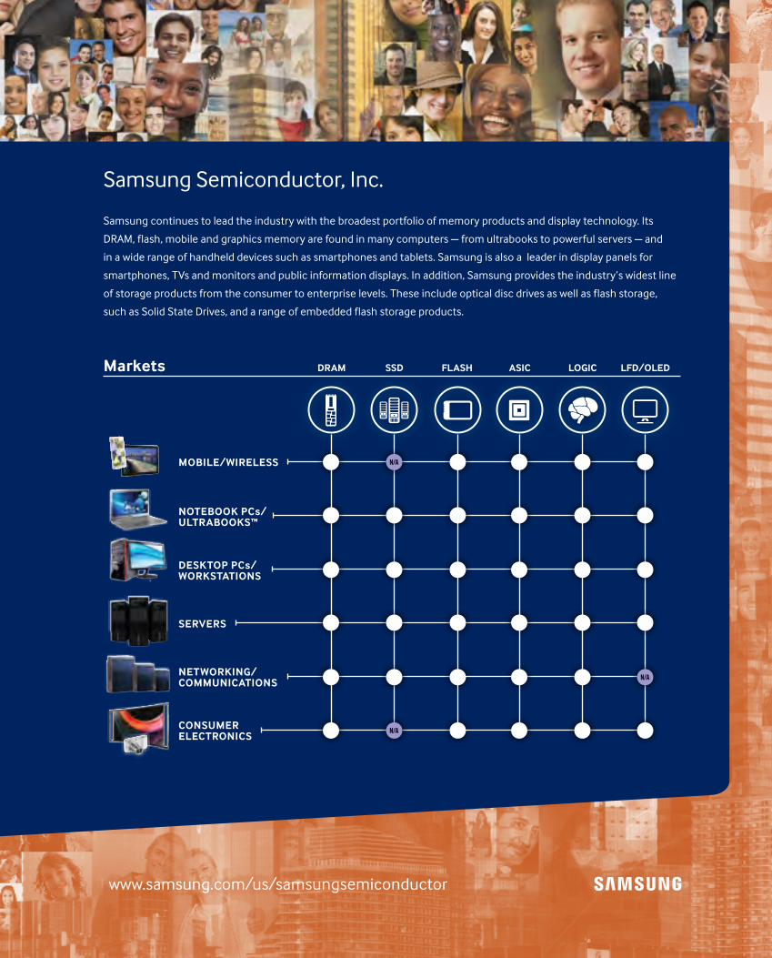
MOBILE/WIRELESS
NOTEBOOK PCs/ULTRABOOKS™
DESKTOP PCs/WORKSTATIONS
NETWORKING/ COMMUNICATIONS
CONSUMER ELECTRONICS
Markets
SERVERS
Samsung continues to lead the industry with the broadest portfolio of memory products and display technology. Its
DRAM, flash, mobile and graphics memory are found in many computers — from ultrabooks to powerful servers — and
in a wide range of handheld devices such as smartphones and tablets. Samsung is also a leader in display panels for
smartphones, TVs and monitors and public information displays. In addition, Samsung provides the industry’s widest line
of storage products from the consumer to enterprise levels. These include optical disc drives as well as flash storage,
such as Solid State Drives, and a range of embedded flash storage products.
Samsung Semiconductor, Inc.
DRAM FLASH ASIC LOGICSSD LFD/OLED

DR
AM
TaBLE OF CONTENTS
//
DRaM PAGES 4–14
samsung.com/dram
• DDR4 SDRAM
• DDR3 SDRAM
• DDR2 SDRAM
• Graphics DRAM
• Mobile DRAM
• Ordering Info
FLASH - SSD PAGES 15–16
samsung.com/flash
• eMMC
• Universal Flash Storage (UFS)
• Solid State Drives (SSD)
MULTI-ChIP PaCKaGES PAGES 17–18
samsung.com/mcp
• eMMC + LPDDR2 • eMMC + LPDDR3
STORaGE PAGES 19–21
samsung.com/flash-ssd
• Solid State Drives (SSD)
DISPLayS PAGES 22-23
samsungdisplay.com
• Public Information Display (PID) Product Classification
• SNB/UNB
• Indoor PID• E-Board• Outdoor PID
CONTaCTS PAGES 24–25
samsung.com/semiconductor/sales-network
• Sales Representatives and DistributorsD
Ra
M

samsung.com/dram4 1H 2016DDR4 SDRAM samsung.com/dram
DDR4 SDRAM REGISTERED MODULESDensity Voltage Organization Part Number Composition Compliance Speed (Mbps) Ranks Production
4GB 1.2V 1G x 72M393A5143DB0-CPB 4Gb (512M x8) * 9 Lead Free & Halogen Free, Flip Chip 2133 1 Now
M393A5143DB0-CRC 4Gb (512M x8) * 9 Lead Free & Halogen Free, Flip Chip 2400 1 Now
8GB 1.2V 1G x 72
M393A1G40DB0-CPB 4Gb (1G x4) * 18 Lead Free & Halogen Free, Flip Chip 2133 1 Now
M393A1G40DB1-CRC 4Gb (1G x4) * 18 Lead Free & Halogen Free, Flip Chip 2400 1 Now
M393A1G43DB0-CPB 4Gb (512M x8) * 18 Lead Free & Halogen Free, Flip Chip 2133 2 Now
M393A1G43DB1-CRC 4Gb (512M x8) * 18 Lead Free & Halogen Free, Flip Chip 2400 2 Now
M393A1G40EB1-CPB 4Gb (1G x4) * 18 Lead Free & Halogen Free, Flip Chip 2133 1 Now
M393A1G40EB1-CRC 4Gb (1G x4) * 18 Lead Free & Halogen Free, Flip Chip 2400 1 Now
M393A1G43EB1-CPB 4Gb (512M x8) * 18 Lead Free & Halogen Free, Flip Chip 2133 2 Now
M393A1G43EB1-CRC 4Gb (512M x8) * 18 Lead Free & Halogen Free, Flip Chip 2400 2 Now
16GB 1.2V 2G x 72
M393A2G40DB0-CPB 4Gb (1G x4) * 36 Lead Free & Halogen Free, Flip Chip 2133 2 Now
M393A2G40DB1-CRC 4Gb (1G x4) * 36 Lead Free & Halogen Free, Flip Chip 2400 2 Now
M393A2G40EB1-CPB 4Gb (1G x4) * 36 Lead Free & Halogen Free, Flip Chip 2133 2 Now
M393A2G40EB1-CRC 4Gb (1G x4) * 36 Lead Free & Halogen Free, Flip Chip 2400 2 Now
M393A2K40BB0-CPB 8Gb (2G x4) * 18 Lead Free & Halogen Free, Flip Chip 2133 1 Now
M393A2K40BB1-CRC 8Gb (2G x4) * 18 Lead Free & Halogen Free, Flip Chip 2400 1 Now
M393A2K43BB1-CPB/CRC 8Gb (1G x8) * 18 Lead Free & Halogen Free, Flip Chip 2133/2400 2 Now
32GB 1.2V 4G x 72M393A4K40BB0-CPB 8Gb (2G x4) * 36 Lead Free & Halogen Free, Flip Chip 2133 2 Now
M393A4K40BB1-CRC 8Gb (2G x4) * 36 Lead Free & Halogen Free, Flip Chip 2400 2 Now
64GB TSV 1.2V 8G x 72
M393A8G40D40-CRB 4Gb 4H TSV (4G x4) * 36 Lead Free & Halogen Free, 4High TSV 2133 8 Now
M393A8K40B21-CRB 8Gb 2H TSV (4G x4) * 36 Lead Free & Halogen Free, 2High TSV 2133 4 Now
M393A8K40B21-CTC 8Gb 2H TSV (4G x4) * 36 Lead Free & Halogen Free, 2High TSV 2400 4 Now
128GB TSV
1.2V 16G x 72 M393AAK40B41-CTC 8Gb 4H TSV (8G x4) * 36 Lead Free & Halogen Free, 4High TSV 2400 8 Now
Notes: DDR4 4Gb (D die) based 0 = IDT 2 = Montage 3 = Inphi PB = DDR4-2133(15-15-15) 0 = IDT 4 = Montage RC = DDR4-2400(17-17-17) DDR4 4Gb (E die) based 0 = IDT 4 = Montage 3 = Inphi PB = DDR4-2133(15-15-15) 0 = IDT 4 = Montage 3 = Inphi RC = DDR4-2400(17-17-17) DDR4 (B Die) 8Gb based 0 = IDT 4 = Montage PB = DDR4-2133(15-15-15) 0 = IDT 4 = Montage 3 = Inphi RC = DDR4-2400(17-17-17)
DDR4 SDRAM COMPONENTSDensity Voltage Organization Part Number # Pins-Package Compliance Speed (Mbps) Dimensions Production
4Gb 1.2V
1G x 4 K4A4G045WD-BCRC/PB 78 Ball -FBGA Lead Free & Halogen Free, Flip Chip 2400/2133 7.5x11mm Now
512M x 8 K4A4G085WD-BCRC/PB 78 Ball -FBGA Lead Free & Halogen Free, Flip Chip 2400/2133 7.5x11mm Now
256M x 16 K4A4G165WD-BCRC/PB 96 Ball -FBGA Lead Free & Halogen Free, Flip Chip 2400/2133 7.5x13.3mm Now
1G x 4 K4A4G045WE-BCRC/PB 78 Ball -FBGA Lead Free & Halogen Free, Flip Chip 2400/2133 7.5x11mm Now
512M x 8 K4A4G085WE-BCRC/PB 78 Ball -FBGA Lead Free & Halogen Free, Flip Chip 2400/2133 7.5x11mm Now
256M x 16 K4A4G165WE-BCRC/PB 96 Ball -FBGA Lead Free & Halogen Free, Flip Chip 2400/2133 7.5x13.3mm Now
8Gb 1.2V1G x 8 K4A8G085WB-BCRC/PB 78 ball FBGA Lead Free & Halogen Free, Flip Chip 2400/2133 7.5x11mm Now
512M x16 K4A8G165WB-BCRC/PB 96 Ball -FBGA Lead Free & Halogen Free, Flip Chip 2400/2133 7.5x13.3mm CS: '15, 1Q
DDR4 SDRAM Load Reduced REGISTERED MODULESDensity Voltage Organization Part Number Composition Compliance Speed (Mbps) Ranks Production
32GB 1.2V 4G x 72
M386A4G40DM0-CPB 4Gb DDP (2G x4) * 36 Lead Free & Halogen Free, DDP 2133 4 Now
M386A4G40DM1-CRC 4Gb DDP (2G x4) * 36 Lead Free & Halogen Free, DDP 2400 4 Now
M386A4K40BB0-CRC5 8G (2Gx4)*36 Lead Free & Halogen Free, Flip Chip 2400 2 Now
64GB 1.2V 8G x 72 M386A8K40BM1-CPB/CRC 8Gb DDP (4G x4) * 36 Lead Free & Halogen Free, DDP 2133/2400 4 Now
128GB 1.2V 16G x 72 M386AAK40B40-CUC 8Gb 4H TSV (8G x4) * 36 Lead Free & Halogen Free, DDP 2400 8 Now
Notes: DDR4 4Gb (D die) based 0 = IDT 2 = Montage PB = DDR4-2133(15-15-15) 5 = IDT 4 = Montage RC = DDR4-2400(17-17-17) DDR4 (B Die) 8Gb based 0 = IDT 4 = Montage PB = DDR4-2133(15-15-15) 5 = IDT 4 = Montage RC = DDR4-2400(17-17-17)

samsung.com/dram 51H 2016
DR
AM
DDR4 SDRAM
DDR4 SDRAM UNBUFFERED MODULESDensity Voltage Organization Part Number Composition Compliance Speed (Mbps) Ranks Production
4GB 1.2V 512M x 64
M378A5143DB0-CPB 4Gb (512M x8) *8 Lead Free & Halogen Free 2133 1 Now
M378A5143EB1-CPB 4Gb (512M x8) *8 Lead Free & Halogen Free 2133 1 Now
M378A5143EB2-CRC 4Gb (512M x8) *8 Lead Free & Halogen Free 2400 1 Now
8GB 1.2V 1G x 64
M378A1G43DB0-CPB 4Gb (512M x8) *16 Lead Free & Halogen Free 2133 2 Now
M378A1G43EB1-CRC 4Gb (512M x8) *16 Lead Free & Halogen Free 2400 2 Now
M378A1K43BB1-CPB 8Gb (1G x8) *8 Lead Free & Halogen Free 2133 2 Now
M378A1K43BB2-CRC 8Gb (1G x8) *8 Lead Free & Halogen Free 2400 2 Now
16GB 1.2V 2G x 64 M378A2K43BB1-CPB/CRC 8Gb (1G x8) * 16 Lead Free & Halogen Free 2133/2400 2 Now
Notes: PB = DDR4-2133(15-15-15) RC = DD R4-2400(17-17-17)
DDR4 SDRAM ECC UNBUFFERED MODULESDensity Voltage Organization Part Number Composition Compliance Speed (Mbps) Ranks Production
4GB 1.2V 512M x72 M391A5143EB1-CPB/CRC 4Gb (512M x8) * 9 Lead Free & Halogen Free, Flip Chip 2133/2400 1 Now
8GB 1.2V 1G x72M391A1G43DB0-CPB/CRC 4Gb (512M x8) * 18 Lead Free & Halogen Free, Flip Chip 2133/2400 2 Now
M391A1K43BB1-CPB/CRC 8Gb (1G x8) * 9 Lead Free & Halogen Free, Flip Chip 2133/2400 2 Now
16GB 1.2V 2G x72 M391A2K43BB1-CPB/CRC 8Gb (1G x8) * 18 Lead Free & Halogen Free, Flip Chip 2133/2400 2 Now
Notes: PB = DDR4-2133(15-15-15) RC = DDR4-2400(17-17-17)
DDR4 SDRAM ECC SODIMM MODULESDensity Voltage Organization Part Number Composition Compliance Speed (Mbps) Ranks Production
8GB 1.2V 1G x 72
M474A1G43DB0-CPB 4Gb (512M x8) * 18 Lead Free & Halogen Free, Flip Chip 2133 2 Now
M474A1G43DB1-CRC 4Gb (512M x8) * 18 Lead Free & Halogen Free, Flip Chip 2400 2 Now
M474A1G43EB1-CPB/CRC 4Gb (512M x8) * 18 Lead Free & Halogen Free, Flip Chip 2133/2400 2 Now
16GB 1.2V 2G x 72 M474A2K43BB1-CPB/RC 8Gb (1G x8) * 18 Lead Free & Halogen Free, Flip Chip 2133/2400 2 Now
DDR4 SDRAM SODIMM MODULESDensity Voltage Organization Part Number Composition Compliance Speed (Mbps) Ranks Production
4GB 1.2V 512M x 64M471A5143DB0-CPB 4Gb (512M x8) * 8 Lead Free & Halogen Free 2133 1 Now
M471A5143EB0-CPB/CRC 4Gb (512M x8) * 8 Lead Free & Halogen Free 2133/2400 1 Now
8GB 1.2V 1G x 64
M471A1G43DB0-CPB 4Gb (512M x8) * 16 Lead Free & Halogen Free 2133 2 Now
M471A1G43EB1-CPB/CRC 4Gb (512M x8) * 16 Lead Free & Halogen Free 2133/2400 2 Now
M471A1K43BB1-CPB/CRC 8Gb (1Gx8)*8 Lead Free & Halogen Free 2133/2400 1 Now
16GB 1.2V 2G x 64 M471A2K43BB1-CPB/CRC 8Gb (1G x8) * 16 Lead Free & Halogen Free 2133/2400 2 Now
Notes: PB = DDR4-2133(15-15-15) RC = DDR4-2400(17-17-17)
DDR4 SDRAM VLP REGISTERED MODULESDensity Voltage Organization Part Number Composition Compliance Speed (Mbps) Ranks Production
16GB 1.2V 2G x 72M392A2G40DM0-CPB 4Gb DDP (2G x4) * 18 Lead Free & Halogen Free, DDP 2133 2 Now
M392A2K43BB0-CPB/RC 8Gb (1G x8) * 18 Lead Free & Halogen Free, Flip Chip 2133/2400 2 Now
32GB 1.2V 4G x 72 M392A4K40BM0-CPB/RC 8Gb DDP (4G x4) * 18 Lead Free & Halogen Free, DDP 2133/2400 2 Now
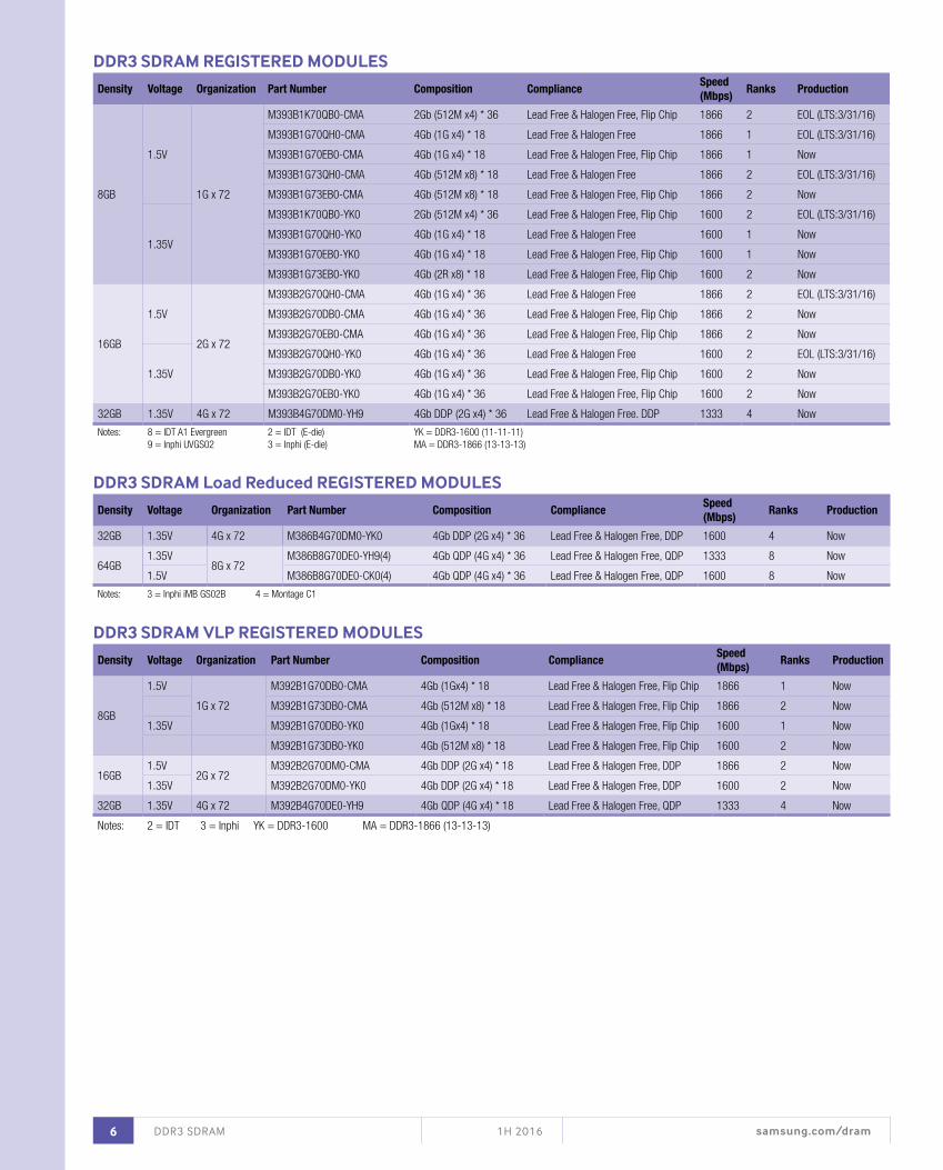
samsung.com/dram6 1H 2016DDR3 SDRAM
DDR3 SDRAM VLP REGISTERED MODULES
Density Voltage Organization Part Number Composition ComplianceSpeed (Mbps)
Ranks Production
8GB
1.5V
1G x 72
M392B1G70DB0-CMA 4Gb (1Gx4) * 18 Lead Free & Halogen Free, Flip Chip 1866 1 Now
M392B1G73DB0-CMA 4Gb (512M x8) * 18 Lead Free & Halogen Free, Flip Chip 1866 2 Now
1.35V M392B1G70DB0-YK0 4Gb (1Gx4) * 18 Lead Free & Halogen Free, Flip Chip 1600 1 Now
M392B1G73DB0-YK0 4Gb (512M x8) * 18 Lead Free & Halogen Free, Flip Chip 1600 2 Now
16GB1.5V
2G x 72M392B2G70DM0-CMA 4Gb DDP (2G x4) * 18 Lead Free & Halogen Free, DDP 1866 2 Now
1.35V M392B2G70DM0-YK0 4Gb DDP (2G x4) * 18 Lead Free & Halogen Free, DDP 1600 2 Now
32GB 1.35V 4G x 72 M392B4G70DE0-YH9 4Gb QDP (4G x4) * 18 Lead Free & Halogen Free, QDP 1333 4 Now
Notes: 2 = IDT 3 = Inphi YK = DDR3-1600 MA = DDR3-1866 (13-13-13)
DDR3 SDRAM REGISTERED MODULES
Density Voltage Organization Part Number Composition ComplianceSpeed (Mbps)
Ranks Production
8GB
1.5V
1G x 72
M393B1K70QB0-CMA 2Gb (512M x4) * 36 Lead Free & Halogen Free, Flip Chip 1866 2 EOL (LTS:3/31/16)
M393B1G70QH0-CMA 4Gb (1G x4) * 18 Lead Free & Halogen Free 1866 1 EOL (LTS:3/31/16)
M393B1G70EB0-CMA 4Gb (1G x4) * 18 Lead Free & Halogen Free, Flip Chip 1866 1 Now
M393B1G73QH0-CMA 4Gb (512M x8) * 18 Lead Free & Halogen Free 1866 2 EOL (LTS:3/31/16)
M393B1G73EB0-CMA 4Gb (512M x8) * 18 Lead Free & Halogen Free, Flip Chip 1866 2 Now
1.35V
M393B1K70QB0-YK0 2Gb (512M x4) * 36 Lead Free & Halogen Free, Flip Chip 1600 2 EOL (LTS:3/31/16)
M393B1G70QH0-YK0 4Gb (1G x4) * 18 Lead Free & Halogen Free 1600 1 Now
M393B1G70EB0-YK0 4Gb (1G x4) * 18 Lead Free & Halogen Free, Flip Chip 1600 1 Now
M393B1G73EB0-YK0 4Gb (2R x8) * 18 Lead Free & Halogen Free, Flip Chip 1600 2 Now
16GB
1.5V
2G x 72
M393B2G70QH0-CMA 4Gb (1G x4) * 36 Lead Free & Halogen Free 1866 2 EOL (LTS:3/31/16)
M393B2G70DB0-CMA 4Gb (1G x4) * 36 Lead Free & Halogen Free, Flip Chip 1866 2 Now
M393B2G70EB0-CMA 4Gb (1G x4) * 36 Lead Free & Halogen Free, Flip Chip 1866 2 Now
1.35V
M393B2G70QH0-YK0 4Gb (1G x4) * 36 Lead Free & Halogen Free 1600 2 EOL (LTS:3/31/16)
M393B2G70DB0-YK0 4Gb (1G x4) * 36 Lead Free & Halogen Free, Flip Chip 1600 2 Now
M393B2G70EB0-YK0 4Gb (1G x4) * 36 Lead Free & Halogen Free, Flip Chip 1600 2 Now
32GB 1.35V 4G x 72 M393B4G70DM0-YH9 4Gb DDP (2G x4) * 36 Lead Free & Halogen Free. DDP 1333 4 Now
Notes: 8 = IDT A1 Evergreen9 = Inphi UVGS02
2 = IDT (E-die) 3 = Inphi (E-die)
YK = DDR3-1600 (11-11-11)MA = DDR3-1866 (13-13-13)
DDR3 SDRAM Load Reduced REGISTERED MODULES
Density Voltage Organization Part Number Composition ComplianceSpeed (Mbps)
Ranks Production
32GB 1.35V 4G x 72 M386B4G70DM0-YK0 4Gb DDP (2G x4) * 36 Lead Free & Halogen Free, DDP 1600 4 Now
64GB1.35V
8G x 72M386B8G70DE0-YH9(4) 4Gb QDP (4G x4) * 36 Lead Free & Halogen Free, QDP 1333 8 Now
1.5V M386B8G70DE0-CK0(4) 4Gb QDP (4G x4) * 36 Lead Free & Halogen Free, QDP 1600 8 Now
Notes: 3 = Inphi iMB GS02B 4 = Montage C1

samsung.com/dram 71H 2016
DR
AM
DDR3 SDRAM
DDR3 SDRAM UNBUFFERED MODULES (ECC)Density Voltage Organization Part Number Composition Compliance Speed (Mbps) Ranks Production
4GB1.5V
512Mx72M391B5173EB0-CMA 4Gb (512M x8) * 9 Lead Free & Halogen Free 1866 1 Now
1.35V M391B5173EB0-YK0 4Gb (512M x8) * 9 Lead Free & Halogen Free 1600 1 Now
8GB1.5V
1G x 72
M391B1G73QH0-CMA 4Gb (512M x8) * 18 Lead Free & Halogen Free 1866 2 Now
M391B1G73EB0-CMA 4Gb (512M x8) * 18 Lead Free & Halogen Free 1866 2 Now
1.35V M391B1G73EB0-YK0 4Gb (512M x8) * 18 Lead Free & Halogen Free 1600 2 Now
Notes: YK0 = DDR3-1600 (11-11-11) MA = DDR3-1866 (13-13-13)
DDR3 Non ECC UNBUFFERED MODULESDensity Voltage Organization Part Number Composition Compliance Speed (Mbps) Ranks Production
4GB
1.5V
512M x 64
M378B5173QH0-CK0/CMA 4Gb (512M x8) * 8 Lead Free & Halogen Free 1600/1866 1 EOL(LTS: 3/31/16)
M378B5173DB0-CK0/CMA 4Gb (512M x8) * 8 Lead Free & Halogen Free. Flip Chip 1600/1866 1 Now
M378B5173EB0-CK0/CMA 4Gb (512M x8) * 8 Lead Free & Halogen Free. Flip Chip 1600/1866 1 Now
1.35VM378B5173QH0-YK0/YMA 4Gb (512M x8) * 8 Lead Free & Halogen Free 1600/1866 1 EOL(LTS: 3/31/16)
M378B5173EB0-YK0/*CMA 4Gb (512M x8) * 8 Lead Free & Halogen Free. Flip Chip 1600/1866 1 Now
8GB
1.5V
1G x 64
M378B1G73QH0-CK0/MA 4Gb (512M x8) * 16 Lead Free & Halogen Free 1600/1866 2 EOL(LTS: 3/31/16)
M378B1G73DB0-CK0/MA 4Gb (512M x8) * 16 Lead Free & Halogen Free. Flip Chip 1600/1866 2 Now
M378B1G73EB0-CK0/CMA 4Gb (512M x8) * 16 Lead Free & Halogen Free. Flip Chip 1600/1866 2 Now
1.35VM378B1G73QH0-YK0/MA 4Gb (512M x8) * 16 Lead Free & Halogen Free 1600/1866 2 EOL(LTS: 3/31/16)
M378B1G73EB0-YK0/*CMA 4Gb (512M x8) * 16 Lead Free & Halogen Free. Flip Chip 1600/1866 2 Now
Notes: YK = DDR3-1600 (11-11-11) MA = DDR3-1866 (13-13-13) * 1.35V is compatible to 1.5V
DDR3 SDRAM SODIMM MODULESDensity Voltage Organization Part Number Composition Compliance Speed (Mbps) Ranks Production
4GB 1.35V 512M x 72 M474B5173EB0-YK0 4Gb (512M x8) * 9 Lead Free & Halogen Free, Flip Chip 1866 1 Now
8GB
1.5V
1G x 72
M474B1G73QH0-CMA 4Gb (512M x8) * 18 Lead Free & Halogen Free 1866 2 EOL(LTS: 3/31/16)
M474B1G73EB0-CMA 4Gb (512M x8) * 18 Lead Free & Halogen Free, Flip Chip 1866 2 Now
1.35VM474B1G73QH0-YK0 4Gb (512M x8) * 18 Lead Free & Halogen Free 1600 2 EOL(LTS: 3/31/16)
M474B1G73EB0-YK000 4Gb (512M x8) * 18 Lead Free & Halogen Free, Flip Chip 1600 2 Now

samsung.com/dram8 1H 2016DDR3 & DDR2 SDRAM
DDR3 SDRAM COMPONENTS
Density Voltage Organization Part Number # Pins- Package Compliance Speed (Mbps) Dimensions Production
1Gb
1.5V
128M x 8 K4B1G0846G-BCH9/K0/MA 78 Ball -FBGA Lead Free & Halogen Free, Flip Chip 1333/1600/1866 7.5x11mm Now
128M x 16 K4B1G1646G-BCH9/K0/MA/NB 96 Ball -FBGA Lead Free & Halogen Free, Flip Chip 1333/1600/1866/2133 7.5x13.3mm Now
128M x 8 K4B1G0846I-BCK0/MA/NB 78 Ball -FBGA Lead Free & Halogen Free, Flip Chip 1600/1866/2133 7.5x11mm Now
128M x 16 K4B1G1646I-BCK0/MA/NB 96 Ball -FBGA Lead Free & Halogen Free, Flip Chip 1600/1866/2133 7.5x13.3mm Now
1.35V
128M x 8 K4B1G0846G-BYH9/K0 78 Ball -FBGA Lead Free & Halogen Free, Flip Chip 1333/1600 7.5x11mm Now
128M x 16 K4B1G1646G-BYH9/K0 96 Ball -FBGA Lead Free & Halogen Free, Flip Chip 1333/1600 7.5x13.3mm Now
128M x 8 K4B1G0846I-BYK0/MA 78 Ball -FBGA Lead Free & Halogen Free, Flip Chip 1600/1800 7.5x11mm Now
128M x 16 K4B1G1646I-BYK0/MA 96 Ball -FBGA Lead Free & Halogen Free, Flip Chip 1600/1800 7.5x13.3mm Now
2Gb
1.5V
256M x 8 K4B2G0846Q-BCK0/MA/NB 78 Ball -FBGA Lead Free & Halogen Free, Flip Chip 1600/1866/2133 7.5x11mmEOL(LTS: 3/31/16)
128M x 16 K4B2G1646Q-BCK0/MA/NB 96 Ball -FBGA Lead Free & Halogen Free, Flip Chip 1600/1866/2133 7.5x13.3mmEOL(LTS: 3/31/16)
512M x 8 K4B2G0846F-BCK0/MA/NB 78 Ball -FBGA Lead Free & Halogen Free, Flip Chip 1600/1866/2133 7.5x11mm Now
256M x 16 K4B2G1646F-BCK0/MA/NB 96 Ball -FBGA Lead Free & Halogen Free, Flip Chip 1600/1866/2133 7.5x13.3mm Now
1.35V
512M x 4 K4B2G0446Q-BYK0 78 Ball -FBGA Lead Free & Halogen Free, Flip Chip 1600 7.5x11mmEOL(LTS: 3/31/16)
256M x 8 K4B2G0846Q-BYK0/MA 78 Ball -FBGA Lead Free & Halogen Free, Flip Chip 1600/1866 7.5x11mmEOL(LTS: 3/31/16)
128M x 16 K4B2G1646Q-BYK0/MA 96 Ball -FBGA Lead Free & Halogen Free, Flip Chip 1600/1866 7.5x13.3mmEOL(LTS: 3/31/16)
256M x 8 K4B2G0846F-BK0/MA 78 Ball -FBGA Lead Free & Halogen Free, Flip Chip 1600/1866 7.5x11mm Now
128M x 16 K4B2G1646F-BK0/MA 96 Ball -FBGA Lead Free & Halogen Free, Flip Chip 1600/1866 7.5x13.3mm Now
4Gb
1.5V
512M x 8 K4B4G0846D-BCK0/MA/NB 78 Ball -FBGA Lead Free & Halogen Free, Flip Chip 1600/1866/2133 7.5x11mm Now
256M x 16 K4B4G1646D-BCK0/MA/NB 96 Ball -FBGA Lead Free & Halogen Free, Flip Chip 1600/1866/2133 7.5x13.3mm Now
512M x 8 K4B4G0846E-BCK0/MA/NB 78 Ball -FBGA Lead Free & Halogen Free, Flip Chip 1600/1866/2133 7.5x11mm Now
256M x 16 K4B4G1646E-BCK0/MA/NB 96 Ball -FBGA Lead Free & Halogen Free, Flip Chip 1600/1866/2133 7.5x13.3mm Now
1.35V
1G x 4 K4B4G0446D-BYK0 78 Ball -FBGA Lead Free & Halogen Free, Flip Chip 1600 7.5x11mm Now
512M x 8 K4B4G0846D-BYK0 78 Ball -FBGA Lead Free & Halogen Free, Flip Chip 1600 7.5x11mm Now
256M x 16 K4B4G1646D-BYK0/MA 96 Ball -FBGA Lead Free & Halogen Free, Flip Chip 1600/1866 7.5x13.3mm Now
1G x 4 K4B4G0446E-BYK0/MA 78 Ball -FBGA Lead Free & Halogen Free, Flip Chip 1600/1866 7.5x11mm Now
512M x 8 K4B4G0846E-BYK0/MA 78 Ball -FBGA Lead Free & Halogen Free, Flip Chip 1600/1866 7.5x11mm Now
256M x 16 K4B4G1646E-BYK0/MA 96 Ball -FBGA Lead Free & Halogen Free, Flip Chip 1600/1866 7.5x13.3mm Now
8Gb
1.5V 512M x 16K4B8G1646Q-MCK0/MA 96 Ball -FBGA Lead Free & Halogen Free 1600/1866 11x13.3mm Now
K4G8G1646D-MCK0/MA 96 Ball -FBGA Lead Free & Halogen Free 1600/1866 11x13.3mm Now
1.35V 512M x 16K4B8G1646Q-MYK0 96 Ball -FBGA Lead Free & Halogen Free 1600 11x13.3mm Now
K4G8G1646D-MYK0/ (MA) 96 Ball -FBGA Lead Free & Halogen Free 1600 / (1866) 11x13.3mm Now
Notes: H9 = DDR3-1333 (9-9-9) K0 = DDR3-1600 (11-11-11) MA = DDR3-1866 (13-13-13) NB = DDR3-2133 (14-14-14)
DDR2 SDRAM COMPONENTSDensity Organization Part Number # Pins-Package Dimensions Package Speed (Mbps) Production
512Mb64M x 8 K4T51083QQ-BC(E6/F7/E7/F8) 60-FBGA 7.5x9.5mm Lead free & Halogen free , Flip chip 667/800/1066 Now
32M x 16 K4T51163QQ-BC(E6/F7/E7/F8) 84-FBGA 7.5x12.5mm Lead free & Halogen free , Flip chip 667/800/1066 Now
1Gb128M x 8 K4T1G084QG-BC(E6/F7/E7/F8) 60-FBGA 7.5x9.5mm Lead free & Halogen free , Flip chip 667/800/1066 Now
64M x 16 K4T1G164QG-BC(E6/F7/E7/F8) 84-FBGA 7.5x12.5mm Lead free & Halogen free , Flip chip 667/800/1066 Now
Notes: E6 = DDR2-667 (5-5-5) E7 = DDR2-800 (5-5-5) F7 = DDR2-800 (6-6-6) F8 = DDR2-1066 (7-7-7)

samsung.com/dram 91H 2016
DR
AM
GRAPHICS DRAM COMPONENTSType Density Organization Part Number Package VDD/VDDQ Speed Bin (MHz) Production
GDDR5
8Gb 256M x 32K4G80325FB-HC(03/28/25) 170-FCFBGA 1.5V/1.5V 6000/7000/8000 Now
K4G80325FB-HC(03/28/25) 170-FCFBGA 1.35V/1.35V 5000/6000/(TBD) Now
4Gb 128M x 32K4G41325FE-HC2(03/28/25/22) 170-FCFBGA 1.5V/1.5V 6000/7000/8000/9000 Now
K4G41325FE-HC2(03/28/25/22) 170-FCFBGA 1.35V/1.35V 5000/6000/7000/TBD Now
gDDR3
4Gb 256M x 16K4W4G1646E-BC(1A/1B) 96-FCFBGA 1.5V/1.5V 2133/2400 Now
K4W4G1646E-BC(1A/1B) 96-FCFBGA 1.35V/1.35V 1866/2133 Now
2Gb 128M x 16
K4W2G1646Q-BC(12/11/1A) 96-FCFBGA 1.5V/1.5V 1600/1866/2133 Now
K4W2G1646Q-BC(1A) 96-FCFBGA 1.35V/1.35V 1866 Now
K4W2G1646Q-BY(12) 96-FCFBGA 1.35V/1.35V 1600 Now
Notes: Package & Speed Bin Codes H: FBGA (Halogen Free & Lead Free) (DDR3)B: FCFBGA (Halogen Free & Lead Free) (DDR3)H: FCFBGA (Halogen Free & Lead Free) (GDDR5)F: FBGA (Halogen Free & Lead Free) (GDDR5)22: 0.22ns (9000Mbps)25: 0.25ns (8000Mbps)28: 0.28ns (7000Mbps)
03: 0.3ns (6000Mbps)04: 0.4ns (5000Mbps)05: 0.5ns (4000Mbps)1B: 8.3ns (2400Mbps gDDR3)1A: 1.0ns (2133Mbps gDDR3)11: 1.1ns (1866Mbps) 12: 1.25ns (1600Mbps)
GRAPHICS & MOBILE DRAM
MOBILE DRAM COMPONENTSType Density Organization Part Number Package Power Production
LPDDR3
8Gb
1CH x 32K4E8E324EB-EGCF 178-FBGA, 11x11.5, SDP, 1866Mbps 1.8V/1.2V/1.2V Now
K4E8E324EB-AGCF 168-FBGA, 12x12, SDP, 1866Mbps 1.8V/1.2V/1.2V Now
2CH x 32
K3QF1F10EM-AGCE 253-FBGA, 11x11.5, DDP, 1600Mbps 1.8V/1.2V/1.2V Now
K3QF1F10EM-BGCE 216-FBGA, 12x12, DDP, 1600Mbps 1.8V/1.2V/1.2V Now
K3QF1F10EM-FGCE 256-FBGA, 14x14, DDP, 1600Mbps 1.8V/1.2V/1.2V Now
12Gb 1CH x32K4E2E304EA-AGCF 168-FBGA, 12x12, DDP, 1866Mbps 1.8V/1.2V/1.2V Now
K4E2E304EA-AGCF 168-FBGA, 12x12, DDP, 1866Mbps 1.8V/1.2V/1.2V Now
16Gb
1CH x 32K4E6E304EB-EGCF 178-FBGA, 11x11.5, DDP, 1866Mbps 1.8V/1.2V/1.2V Now
K4E6E304EB-AGCF 168-FBGA, 12x12, DDP, 1866Mbps 1.8V/1.2V/1.2V Now
2CH x 32
K3QF2F20BM-AGCF 253-FBGA, 11x11.5, DDP, 1866Mbps 1.8V/1.2V/1.2V Now
K3QF3F30BM-BGCF 216-FBGA, 12x12, DDP, 1866Mbps 1.8V/1.2V/1.2V Now
K3QF3F30BM-FGCF 256-FBGA, 14x14, DDP, 1866Mbps 1.8V/1.2V/1.2V Now
K3QF3F30BM-QGCF 216-FBGA, 15x15, DDP, 1866Mbps 1.8V/1.2V/1.2V Now
24Gb
1CH x 32 K4EHE304EA-AGCF 168-FBGA, 12x12, QDP, 1866Mbps 1.8V/1.2V/1.2V Now
2CH x 32
K3QF6F60AM-BGCF 216-FBGA, 12x12, QDP, 1866Mbps 1.8V/1.2V/1.2V Now
K3QF6F60AM-FGCF 256-FBGA, 14x14, QDP, 1866Mbps 1.8V/1.2V/1.2V Now
K3QF6F60AM-QGCF 216-FBGA, 15x15, QDP, 1866Mbps 1.8V/1.2V/1.2V Now
32Gb
1CH x 32 K4EBE304EB-EGCF 178-FBGA, 11x11.5, QDP, 1866Mbps 1.8V/1.2V/1.2V Now
2CH x 32K3QF4F40BM-AGCF 253-FBGA, 11x11.5, QDP, 1866Mbps 1.8V/1.2V/1.2V Now
K3QF4F40BM-FGCF 256-FBGA, 14x14, QDP, 1866Mbps 1.8V/1.2V/1.2V Now
LPDDR4
8Gb 2CH x 16 K4F8E304HB-MGCJ 200-FBGA, 10x15, SDP, 3733Mbps 1.8V/1.1V/1.1V Now
12Gb 2CH x 16 K4F2E3S4HM-MGCJ 200-FBGA, 10x15, SDP, 3733Mbps 1.8V/1.1V/1.1V Now
16Gb2CH x 16 K4F6E304HB-MGCJ 200-FBGA, 10x15, DDP, 3733Mbps 1.8V/1.1V/1.1V Now
4CH x 16 K3RG1G10BM-MGCH 366-FBGA, 15x15, DDP, 3200Mbps 1.8V/1.1V/1.1V Now
24Gb
2CH x 16 K4FHE3D4HM-MFCH 200-FBGA, 10x15, DDP, 3200Mbps 1.8V/1.1V/1.1V CS
4CH x 16K3RG4G40MM-AGCH 272-FBGA, 15x15, DDP, 3200Mbps 1.8V/1.1V/1.1V CS
K3RG4G40MM-MGCJ 366-FBGA, 15x15, DDP, 3733Mbps 1.8V/1.1V/1.1V Now
32Gb 4CH x 16
K3RG2G20BM-AGCH 272-FBGA, 15x15, QDP, 3200Mbps 1.8V/1.1V/1.1V Now
K3RG2G20BM-MGCJ 366-FBGA, 15x15, QDP, 3733Mbps 1.8V/1.1V/1.1V Now
K3RG2G20BM-FGCH 432-FBGA, 15x15, QDP, 3200Mbps 1.8V/1.1V/1.1V CS
48Gb 4CH x 16 K3RG6G60MM-MGCJ 366-FBGA, 15x15, QDP, 3733Mbps 1.8V/1.1V/1.1V CS

samsung.com/dram10 1H 2016
1. Memory (K)
2. DRAM: 4
3. DRAM Type
B: DDR3 SDRAM
D: GDDR SDRAM
G: GDDR5 SDRAM
H: DDR SDRAM
J: GDDR3 SDRAM
M: Mobile SDRAM
N: SDDR2 SDRAM
S: SDRAM
T: DDR SDRAM
U: GDDR4 SDRAM
V: Mobile DDR SDRAM Power Efficient Address
W: SDDR3 SDRAM
X: Mobile DDR SDRAM
Y: XDR DRAM
Z: Value Added DRAM
4. Density
10: 1G, 8K/32ms
16: 16M, 4K/64ms
26: 128M, 4K/32ms
28: 128M, 4K/64ms
32: 32M, 2K/32ms
50: 512M, 32K/16ms
51: 512M, 8K/64ms
52: 512M, 8K/32ms
54: 256M, 16K/16ms
55: 256M, 4K/32ms
56: 256M, 8K/64ms
62: 64M, 2K/16ms
64: 64M, 4K/64ms
68: 768M, 8K/64ms
1G: 1G, 8K/64ms
2G: 2G, 8K/64ms
4G: 4G, 8K/64ms
5. Bit Organization
02: x 2
04: x 4
06: x 4 Stack (Flexframe)
07: x 8 Stack (Flexframe)
08: x 8
15: x 16 (2CS)
16: x 16
26: x 4 Stack (JEDEC Standard)
27: x 8 Stack (JEDEC Standard)
30: x 32 (2CS, 2CKE)
31: x 32 (2CS)
32: x 32
6. # of Internal Banks
2: 2 Banks
3: 4 Banks
4: 8 Banks
5: 16 Banks
7. Interface ( VDD, VDDQ)
2: LVTTL, 3.3V, 3.3V
4: LVTTL, 2.5V, 2.5V
5: SSTL-2 1.8V, 1.8V
6: SSTL-15 1.5V, 1.5V
8: SSTL-2, 2.5V, 2.5V
A: SSTL, 2.5V, 1.8V
F: POD-15 (1.5V,1.5V)
H: SSTL_2 DLL, 3.3V, 2.5V
M: LVTTL, 1.8V, 1.5V
N: LVTTL, 1.5V, 1.5V
P: LVTTL, 1.8V, 1.8V
Q: SSTL-2 1.8V, 1.8V
R: SSTL-2, 2.8V, 2.8V
U: DRSL, 1.8V, 1.2V
8. Generation
A: 2nd Generation
B: 3rd Generation
C: 4th Generation
D: 5th Generation
E: 6th Generation
F: 7th Generation
G: 8th Generation
H: 9th Generation
I: 10th Generation
J: 11th Generation
K: 12th Generation
M: 1st Generation
N: 14th Generation
Q: 17th Generation
9. Package Type
DDR2 DRAML: TSOP II (Lead-free & Halogen-free)
H: FBGA (Lead-free & Halogen-free)
F: FBGA for 64Mb DDR (Lead-free & Halogen-free)
6: sTSOP II (Lead-free & Halogen-free)
T: TSOP II
N: sTSOP II
G: FBGA
U: TSOP II (Lead-free)
V: sTSOP II (Lead-free)
Z: FBGA (Lead-free)
DDR2 SDRAMZ: FBGA (Lead-free)
J: FBGA DDP (Lead-free)
Q: FBGA QDP (Lead-free)
H: FBGA (Lead-free & Halogen-free)
M: FBGA DDP (Lead-free & Halogen-free)
E: FBGA QDP (Lead-free & Halogen-free)
T: FBGA DSP (Lead-free & Halogen-free, Thin)
DDR3 SDRAMZ: FBGA (Lead-free)
H: FBGA (Halogen-free & Lead-free)
Graphics MemoryQ: TQFP
U: TQFP (Lead Free)
G: 84/144 FBGA
V: 144 FBGA (Lead Free)
Z: 84 FBGA (Lead Free)
T: TSOP
L: TSOP (Lead Free)
A: 136 FBGA
B: 136 FBGA (Lead Free)
H: FBGA (Hologen Free & Lead Free)
E: 100 FBGA (Hologen Free & Lead Free)
SDRAML TSOP II (Lead-free & Halogen-free)
N: STSOP II
T: TSOP II
U: TSOP II (Lead-free)
V: sTSOP II (Lead-free)
COMPONENT DRAM ORDERING INFORMATION1 2 3 4 5 6 7 8 9 10 11
K 4 T XX XX X X X X X XX
SAMSUNG Memory
DRAM
DRAM Type
Density
Bit Organization
Speed
Temp & Power
Package Type
Generation
Interface (VDD, VDDQ)
Number of Internal Banks
DRAM Ordering Information

samsung.com/dram 111H 2016
DR
AM
COMPONENT DRAM ORDERING INFORMATION1 2 3 4 5 6 7 8 9 10 11
K 4 T XX XX X X X X X XX
XDR DRAMJ: BOC(LF) P: BOC
Mobile DRAMLeaded/Lead FreeG/A: 52balls FBGA Mono
R/B: 54balls FBGA Mono
X/Z: 54balls BOC Mono
J/V: 60(72)balls FBGA Mono 0.5pitch
L /F: 60balls FBGA Mono 0.8pitch
S/D: 90balls FBGA
Monolithic (11mm x 13mm)F/H: Smaller 90balls FBGA Mono
Y/P: 54balls CSP DDP
M/E: 90balls FBGA DDP
10. Temp & Power - COMMON (Temp, Power)
C: Commercial, Normal (0’C – 95’C) & Normal
Power
C: (Mobile Only) Commercial (-25 ~ 70’C), Normal
Power
J: Commercial, Medium
L: Commercial, Low (0’C – 95’C) & Low Power
L: (Mobile Only) Commercial, Low, i-TCSR
F: Commercial, Low, i-TCSR & PASR & DS
E: Extended (-25~85’C), Normal
N: Extended, Low, i-TCSR
G: Extended, Low, i-TCSR & PASR & DS
I: Industrial, Normal (-40’C – 85’C) & Normal
Power
P: Industrial, Low (-40’C – 85’C) & Low Power
H: Industrial, Low, i-TCSR & PASR & DS
11. Speed (Wafer/Chip Biz/BGD: 00)
DDR SDRAMCC: DDR400 (200MHz @ CL=3, tRCD=3, tRP=3)
B3: DDR333 (166MHz @ CL=2.5, tRCD=3,
tRP=3) *1
A2: DDR266 (133MHz @ CL=2 , tRCD=3, tRP=3)
B0: DDR266 (133MHz @ CL=2.5, tRCD=3,
tRP=3)Note 1: "B3" has compatibility with "A2" and "B0"
DDR2 SDRAMCC: DDR2-400 (200MHz @ CL=3, tRCD=3,
tRP=3)
D5: DDR2-533 (266MHz @ CL=4, tRCD=4,
tRP=4)
E6: DDR2-667 (333MHz @ CL=5, tRCD=5,
tRP=5)
F7: DDR2-800 (400MHz @ CL=6, tRCD=6,
tRP=6)
E7: DDR2-800 (400MHz @ CL=5, tRCD=5,
tRP=5)
DDR3 SDRAMF7: DDR3-800 (400MHz @ CL=6, tRCD=6,
tRP=6)
F8: DDR3-1066 (533MHz @ CL=7, tRCD=7,
tRP=7)
G8: DDR3-1066 (533MHz @ CL=8, tRCD=8,
tRP=8)
H9: DDR3-1333 (667MHz @ CL=9, tRCD=9,
tRP=9)
K0: DDR3-1600 (800MHz @ CL=11, tRCD=11,
tRP=11)
MA: DDR3-1866 (933MHz @ CL=13, tRCD=13,
tRP=13)
NB: DDR3-2133 (1067MHz @ CL=14, tRCD=14,
tRP=14)
Graphics Memory18: 1.8ns (550MHz)
04: 0.4ns (2500MHz)
20: 2.0ns (500MHz)
05: 0.5ns (2000MHz)
22: 2.2ns (450MHz)
5C: 0.56ns (1800MHz)
25: 2.5ns (400MHz)
06: 0.62ns (1600MHz)
2C: 2.66ns (375MHz)
6A: 0.66ns (1500MHz)
2A: 2.86ns (350MHz)
07: 0.71ns (1400MHz)
33: 3.3ns (300MHz)
7A: 0.77ns (1300MHz)
36: 3.6ns (275MHz)
08: 0.8ns (1200MHz)
40: 4.0ns (250MHz)
09: 0.9ns (1100MHz)
45: 4.5ns (222MHz)
1 : 1.0ns (1000MHz)
50/5A: 5.0ns (200MHz)
1 : 1.1ns (900MHz)
55: 5.5ns (183MHz)
12: 1.25ns (800MHz)
60: 6.0ns (166MHz)
14: 1.4ns (700MHz)
16: 1.6ns (600MHz)
SDRAM (Default CL=3)50: 5.0ns (200MHz CL=3)
60: 6.0ns (166MHz CL=3)
67: 6.7ns
75: 7.5ns PC133 (133MHz CL=3)
XDR DRAMA2: 2.4Gbps, 36ns, 16Cycles
B3: 3.2Gbps, 35ns, 20Cycles
C3: 3.2Gbps, 35ns, 24Cycles
C4: 4.0Gbps, 28ns, 24Cycles
DS: Daisychain Sample
Mobile-SDRAM60: 166MHz, CL 3
75: 133MHz, CL 3
80: 125MHz, CL 3
1H: 105MHz, CL 2
1L: 105MHz, CL 3
15: 66MHz, CL 2 & 3
Mobile-DDRC3: 133MHz, CL 3
C2: 100MHz, CL 3
C0: 66MHz, CL 3Note: All Lead-free and Halogen-free products are in compliance with RoHS
SAMSUNG Memory
DRAM
DRAM Type
Density
Bit Organization
Speed
Temp & Power
Package Type
Generation
Interface (VDD, VDDQ)
Number of Internal Banks
DRAM Ordering Information

samsung.com/dram12 1H 2016DRAM Ordering Information
MODULE DRAM ORDERING INFORMATION1 2 3 4 5 6 7 8 9 10 11 12 13
M X XX T XX X X X X X X XX X
1. Memory Module: M
2. DIMM Type
3: DIMM
4: SODIMM
3. Data bits
12: x 72 184pin Low Profile Registered DIMM
63: x 63 PC100/PC133 μSODIMM with SPD
for 144pin
64: x 64 PC100/PC133 SODIMM with SPD
for 144pin (Intel/JEDEC)
66: x 64 Unbuffered DIMM with SPD for
144pin/168pin (Intel/JEDEC)
68: x 64 184pin Unbuffered DIMM
70: x 64 200pin Unbuffered SODIMM
71: x 64 204pin Unbuffered SODIMM
74: x 72/ECC Unbuffered DIMM with SPD
for 168pin (Intel/JEDEC)
77: x 72/ECC PLL + Register DIMM with SPD
for 168pin (Intel PC100)
78: x 64 240pin Unbuffered DIMM
81: x 72 184pin ECC unbuffered DIMM
83: x 72 184pin Registered DIMM
90: x 72/ECC PLL + Register DIMM
91: x 72 240pin ECC unbuffered DIMM
92: x 72 240pin VLP Registered DIMM
93: x 72 240pin Registered DIMM
95: x 72 240pin Fully Buffered DIMM with SPD
for 168pin (JEDEC PC133)
4. DRAM Component Type
B: DDR3 SDRAM (1.5V VDD)
L: DDR SDRAM (2.5V VDD)
S: SDRAM
T: DDR2 SDRAM (1.8V VDD)
5. Depth
09: 8M (for 128Mb/512Mb)
17: 16M (for 128Mb/512Mb)
16: 16M
28: 128M
29: 128M (for 128Mb/512Mb)
32: 32M
33: 32M (for 128Mb/512Mb)
51: 512M
52: 512M (for 512Mb/2Gb)
56: 256M
57: 256M (for 512Mb/2Gb)
59: 256M (for 128Mb/512Mb)
64: 64M
65: 64M (for 128Mb/512Mb)
1G: 1G
1K: 1G (for 2Gb)
6. # of Banks in Comp. & Interface
1: 4K/64mxRef., 4Banks & SSTL-2
2 : 8K/64ms Ref., 4Banks & SSTL-2
2: 4K/64ms Ref., 4Banks & LVTTL (SDR Only)
5: 8K/64ms Ref., 4Banks & LVTTL (SDR Only)
5: 4Banks & SSTL-1.8V
6: 8Banks & SSTL-1.8V
7. Bit Organization
0: x 4
3: x 8
4: x16
6: x 4 Stack (JEDEC Standard)
7: x 8 Stack (JEDEC Standard)
8: x 4 Stack
9: x 8 Stack
8. Generation
A: 2nd Gen.
B: 3rd Gen.
C: 4th Gen.
D: 5th Gen.
E: 6th Gen.
F: 7th Gen.
G: 8th Gen.
M: 1st Gen.
Q: 17th Gen.
9. Package
E: FBGA QDP (Lead-free & Halogen-free)
G: FBGA
H: FBGA (Lead-free & Halogen-free)
J: FBGA DDP (Lead-free)
M: FBGA DDP (Lead-free & Halogen-free)
N: sTSOP
Q: FBGA QDP (Lead-free)
T: TSOP II (400mil)
U: TSOP II (Lead-Free)
V: sTSOP II (Lead-Free)
Z: FBGA (Lead-free)
10. PCB Revision
0: Mother PCB
1: 1st Rev
2: 2nd Rev.
3: 3rd Rev.
4: 4th Rev.
A: Parity DIMM
S: Reduced PCB
U: Low Profile DIMM
11. Temp & Power
C: Commercial Temp. (0°C ~ 95°C) & Normal
Power
L: Commercial Temp. (0°C ~ 95°C) & Low Power
12. Speed
CC: (200MHz @ CL=3, tRCD=3, tRP=3)
D5: (266MHz @ CL=4, tRCD=4, tRP=4)
E6: (333MHz @ CL=5, tRCD=5, tRP=5)
F7: (400MHz @ CL=6, tRCD=6, tRP=6)
E7: (400MHz @ CL=5, tRCD=5, tRP=5)
F8: (533MHz @ CL=7, tRCD=7, tRP=7)
G8: (533MHz @ CL=8, tRCD=8, tRP=8)
H9: (667MHz @ CL=9, tRCD=9, tRP=9)
K0: (800MHz @ CL=10, tRCD=10, tRP=10)
7A: (133MHz CL=3/PC100 CL2)
13. AMB Vendor for FBDIMM
0, 5: Intel
1, 6, 8: IDT
9: MontageNote: All Lead-free and Halogen-free products are in compliance with RoHS
SAMSUNG Memory
DIMM
Data bits
DRAM Component Type
Depth
Number of Banks
Bit Organization
AMB Vendor
Speed
Temp & Power
PCB Revision
Package
Generation

samsung.com/dram 131H 2016
DR
AM
SDRAM Ordering Information
1. Memory Module: M
2. DIMM Type
3: R/LRDIMM
4: SODIMM
3. Data bits
74: x 72 260pin SODIMM
86: x 72 288pin Load Reduced DIMM
93: x 72 288pin Registered DIMM
4. DRAM Component Type
A: DDR4 SDRAM (1.2V VDD)
5. Depth
1G: 1G
2G: 2G
4G: 4G
8G: 8G
1K: 1G (for 8Gb)
2K: 2G (for 8Gb)
6. # of Banks in Comp. & Interface
4: 16Banks & POD-1.2V
7. Bit Organization
0: x 4
3: x 8
8. Component Revision
M: 1st Gen.
A: 2nd Gen.
B: 3rd Gen.
C: 4th Gen.
D: 5th Gen.
E: 6th Gen.
F: 7th Gen.
G: 8th Gen.
9. Package
B: FBGA (Halogen-free & Lead-free, Flip Chip)
M: FBGA (Halogen-free & Lead-free, DDP)
10. PCB Revision
0: None
1: 1st Rev.
2: 2nd Rev.
3: 3rd Rev.
4: 4th Rev.
11. Temp & Power
C: Commercial Temp. (0°C ~ 85°C) &
Normal Power
12. Speed
PB: DDR4-2133
(1066MHz @ CL=15, tRCD=15, tRP=15)
DDR4 SDRAM MODULE ORDERING INFORMATION1 2 3 4 5 6 7 8 9 10 11 12
M X XX A XX X X X X X X XX
Memory Module
DIMM Type
Data bits
DRAM Component Type
Depth
# of Banks in Comp. & Interface
Bit Organization
Speed
Temp & Power
PCB Revision
Package
Component Revision

samsung.com/dram14 1H 2016DDR4 SDRAM Module Ordering Information
1. Samsung Memory: K
2. DRAM: 4
3. DRAM Type
A: DDR4 SDRAM
4. Density
4G: 4Gb
8G: 8Gb
5. Bit Organization
04: x 4
08: x 8
6. # of Internal Banks
5: 16Banks
7. Interface (Vdd, Vddq)
W: POD (1.2V, 1.2V)
8. Revision
M: 1st Gen.
A: 2nd Gen.
B: 3rd Gen.
C: 4th Gen.
D: 5th Gen.
E: 6th Gen.
F: 7th Gen.
G: 8th Gen.
H: 9th Gen.
9. Package Type
B: FBGA (Halogen-free & Lead-free, Flip Chip)
M: FBGA (Halogen-free & Lead-free, DDP)
10. Temp & Power
C: Commercial Temp. (0°C ~ 85°C) &
Normal Power
11. Speed
PB: DDR4-2133
(1066MHz @ CL=15, tRCD=15, tRP=15)
RC: DDR4-2400
(1200MHz @ CL=17, tRCD=17, tRP=17)
DDR4 SDRAM MEMORY ORDERING INFORMATION1 2 3 4 5 6 7 8 9 10 11
K 4 A XX XX X X X X X XX
Samsung Memory
DRAM
DRAM Type
Density
Bit Organization
Speed
Temp & Power
Package Type
Revision
Interface (Vdd, Vddq)
#of Internal Banks

samsung.com/flash 15
FLA
SH -
SSD
1H 2016 Mainstream eMMC, High-Performance eMMC & UFS
Application Interface Bandwidth Density Flash Die Part NumberSeq R/WMB/s
Random R/W IOPS
mm Pkg Size (X,Y,Z) Status
High Performance
UFS 2.0
6Gb/s per laneUp to 2 lanes
256GB 256Gb*8 KLUEG8U1EM-B0B10** 850/260 50K / 30K11.5 x 13.0 x 1.2 Sampling
6Gb/s per lane1 lane only
128GB 128Gb*8 KLUDG8J1CB-B0B10** 460/160
20K / 14K64GB 128Gb*4 KLUCG4J1CB-B0B10**
11.5 x 13.0 x 1.0 MP32GB 64Gb*4 KLUBG4G1CE-B0B10**
16GB 64Gb*2 KLUAG2G1CE-B0B10** 440/80 18K / 10K
Mainstream
eMMC v5.1
400 MB/s
128GB 128Gb*8 KLMDG8JENB-B0410**310/140 14K / 14K 11.5 x 13.0 x 1.0
MP
64GB 128Gb*4 KLMCG4JENB-B0410**
32GB 128Gb*2 KLMBG2JENB-B0410** 310/70 13K / 14K 11.5 x 13.0 x 0.8
eMMC v5.0
64GB 64Gb*8 KLMCG8GEND-B0310**250/100
6.5K / 13K11.5 x 13.0 x 1.0
32GB 64Gb*4 KLMBG4GEND-B0310** 6.5K / 12K
128GB 64Gb*16 KLMDGAWEBD-B0310** 250/45
6K / 5K
11.5 x 13.0 x 1.4
64GB 64Gb*8 KLMCG8WEBD-B0310**260/46 11.5 x 13.0 x 1.0
32GB 64Gb*4 KLMBG4WEBD-B0310**
Low End
eMMC v5.1
400 MB/s
16GB 128Gb*1 KLMAG1JENB-B0410** 285/40 8K / 10K11.5 x 13.0 x 0.8
MP
8GB 64Gb*1 KLM8G1GEME-B0410** 185/40 5.2K / 2.5K
eMMC v5.0
16GB 64Gb*2 KLMAG2GEND-B0310** 230/50 6.5K / 6K11.5 x 13.0 x 0.8
8GB 64Gb*1 KLM8G1GEND-B0310** 160/25 6.5K / 2.5K
4GB 32Gb*1 KLM4G1FEPD-B0310** 120/20 5K / 0.5K 11.0 x 10.0 x 0.8
16GB 64Gb*2 KLMAG2WEPD-B0310** 150/12 5K / 1.2K11.5 x 13.0 x 0.8
8GB 64Gb*1 KLM8G1WEPD-B0310** 140/8 5K / 0.6K
MMC5.1 is backwards compatible with 5.0 & 4.5*Denotes bucket code for latest firmware patch

samsung.com/flash16 1H 2016Solid State Drives
SOLID STATE DRIVES (SSD)Drive Type
Power-loss Protection
Form Factor Interface Connector Product Family
WriteEndurance
Capacity (GB)
Part Number
Client PC/Embedded
No M.2 22 x 80 mm
SATA 3.0 @ 6 Gbit/s
M.2
PM871a
PC Workload
256 MZNLN256HMHQ-00000
512 MZNLN512HMJP-00000
1024 MZNLN1T0HMLH-00000
PCIe Gen 3 x4 @ 32Gbit/s (NVMe)
PM951
128 MZVLV128HCGR-00000
256 MZVLV256HCHP-00000
512 MZVLV512HCJH-00000
Datacenter Yes
2.5" 7mmT
SATA 3.0 @ 6 Gbit/s SFF-8223
PM863a0.8 DWPD for 5 Years
240 MZ7LM240HMHQ-00005
480 MZ7LM480HMHQ-00005
960 MZ7LM960HMJP-00005
1920 MZ7LM1T9HMJP-00005
3840 MZ7LM3T8HMLP-00005
SM863
3.6 DWPDfor 5 Years
120 MZ7KM120HAFD-00005
240 MZ7KM240HAGR-00005
480 MZ7KM480HAHP-00005
960 MZ7KM960HAHP-00005
1920 MZ7KM1T9HAJM-00005
10 DWPDfor 5 Years
100 MZ7KM120HAFD-00005
200 MZ7KM240HAGR-00005
400 MZ7KM480HAHP-00005
800 MZ7KM960HAHP-00005
1600 MZ7KM1T9HAJM-00005
PCIe Gen 3x4 @ 32Gbit/s (NVMe)
U.2 (SFF-8639)
PM9630.8 DWPDfor 5 Years
480 MZQLW480HMHQ-00003
960 MZQLW960HMJP-00003
1920 MZQLW1T9HMJP-00003
3840 MZQLW3T8HMLP-00003
SM963
3.6 DWPDfor 5 Years
960 MZQKW960HMJP-00003
1920 MZQKW1T9HMJP-00003
3840 MZQKW3T8HMLH-00003
10 DWPDfor 5 Years
800 MZQKW960HMJP-00003
1600 MZQKW1T9HMJP-00003
3200 MZQKW3T8HMLH-00003
M.2 22 x 110 mm M.2
PM9630.8 DWPDfor 5 Years
480 MZ1LW480HMHQ-00003
960 MZ1LW960HMJP-00003
1920 MZ1LW1T9HMLS-00003
SM963
3.6 DWPDfor 5 Years
960 MZ1KW960HMJP-00003
1920 MZ1KW1T9HMJP-00003
10 DWPDfor 5 Years
800 MZ1KW960HMJP-00003
1600 MZ1KW1T9HMJP-00003

MC
Ps
samsung.com/mcp 171H 2016 Multi-Chip Packages
Samsung has a portfolio of eMCP products for a variety of devices, such as mobile phones
and tablets. The following illustration shows Samsung’s lineup of eMCP memory solutions,
which can be deployed in almost any application.
eMCP = eMMC + LPDDR3
Samsung eMCP product suite with different densities and types of Mobile DRAM and eMMC
4Gb 6Gb 8Gb 12Gb 16Gb 24Gb
64GB
128GB
32GB
8GB
4GB
16GB
RO
M
R AM
32Gb

samsung.com/mcp18 1H 2016Multi-Chip Packages
eMCP: eMMC + LPDDR3Memory eMMC Density DRAM Density/Organization Voltage (eMMC-DRAM) Package
eMMC & MDRAM
4GB4Gb (x32) 3.3V/1.8V - 1.8V/1.2V 221FBGA 11.5 x 13mm
6Gb (x32) 3.3V/1.8V - 1.8V/1.2V 221FBGA 11.5 x 13mm
8GB8Gb (x32) 3.3V/1.8V - 1.8V/1.2V 221FBGA 11.5 x 13mm
6Gb*2 (x32) 3.3V/1.8V - 1.8V/1.2V 221FBGA 11.5 x 13mm
16GB
8Gb (x32) 3.3V/1.8V - 1.8V/1.2V 221FBGA 11.5 x 13mm
6Gb*2 (x32) 3.3V/1.8V - 1.8V/1.2V 221FBGA 11.5 x 13mm
8Gb*2 (x32) 3.3V/1.8V - 1.8V/1.2V 221FBGA 11.5 x 13mm
6Gb*4 (x32) 3.3V/1.8V - 1.8V/1.2V 221FBGA 11.5 x 13mm
32GB
8Gb*2 (x32) 3.3V/1.8V - 1.8V/1.2V 221FBGA 11.5 x 13mm
6Gb*4 (x32) 3.3V/1.8V - 1.8V/1.2V 221FBGA 11.5 x 13mm
8Gb*4 (x32) 3.3V/1.8V - 1.8V/1.2V 221FBGA 11.5 x 13mm
64GB6Gb*4 (x32) 3.3V/1.8V - 1.8V/1.2V 221FBGA 11.5 x 13mm
8Gb*4 (x32) 3.3V/1.8V - 1.8V/1.2V 221FBGA 11.5 x 13mm
128GB 8Gb*4 (x32) 3.3V/1.8V - 1.8V/1.2V 221FBGA 11.5 x 13mm
ePoP: eMMC + LPDDR3Memory eMMC Density DRAM Density/Organization Voltage (eMMC-DRAM) Package
eMMC & MDRAM
4GB4Gb (x32) 3.3V/1.8V - 1.8V/1.2V 168FBGA 12x12mm
6Gb (x32) 3.3V/1.8V - 1.8V/1.2V 168FBGA 12x12mm
4GB4Gb (x32) 3.3V/1.8V - 1.8V/1.2V 136FBGA 10x10mm
6Gb (x32) 3.3V/1.8V - 1.8V/1.2V 136FBGA 10x10mm
8GB 8Gb (x32) 3.3V/1.8V - 1.8V/1.2V 136FBGA 10x10mm

19
STO
RA
GE
samsung.com/flash-ssd 1H 2016 Solid State Drives
Solid State Drives (SSDs)
Which SSD is right for you? For more information, email: [email protected]
Client PC / Embedded Datacenter Enterprise
LEGACY PC CLIENT
HIGH PERFORMANCE
PC CLIENT
LEGACY DATACENTER
SERIES
HIGH PERFORMANCE
DATACENTER SERIES
ENTERPRISE STORAGE SERIES
High Availability Primary Storage
EXTREME PERFORMANCE
SERIESCache
Applications
PM871a PM951 PM863a PM963 PM1633/PM1633a PM1725a
Host Interface SATA 3.0 @ 6 Gbit/s
PCIe Gen 3 x4 @ 32Gbit/s (NVMe)
SATA 3.0 @ 6 Gbit/s
PCIe Gen 3 x4 @ 32Gbit/s (NVMe)
SAS 3.0 @ 12 Gbit/s
PCIe Gen 3 x8 @ 64Gbit/s (NVMe)
Form Factor M.2 M.2 2.5" M.2 2.5"Add-in Card (HHHL)
Capacity (GB) 256/512/1024 128/256/512240/480/960/1920/3840
480/960/1920480/960/1920/3840/7680/15360
1600/3200/6400
Endurance (up to) Client workload Client workload0.8 DWPD for 5 Years
0.8 DWPD for 5 Years
1-3 DWPD for 5 Years
5-10 DWPDfor 5 Years
Power Consumption (Active) 100 mW 4.5 W 4.1 W 7 W 12 W 25 W
Power Consumption (Idle) 2 mW (DevSlp) 2.5 mW (L1.2) 1.3 W 1.9 W 4 W 7 W
Random Reads (up to) 97,000 IOPS 270,000 IOPS 99,000 IOPS 240,000 IOPS 200,000 IOPS 1,000,000 IOPS
Random Writes (up to) 88,000 IOPS 150,000 IOPS 18,000 IOPS 19,000 IOPS 37,000 IOPS 140,000 IOPS
Sequential Reads (up to) 530 MB/s 1,820 MB/s 540 MB/s 1,000 MB/s 1,400 MB/s 6,000 MB/s
Sequential Writes (up to) 515 MB/s 600 MB/s 480 MB/s 870 MB/s 930 MB/s 1,900 MB/s
MTBF 1.5 Million Hours 1.5 Million Hours 2.0 Million Hours 2.0 Million Hours 2.0 Million Hours 2.0 Million Hours
Uncorrectable Bit Error Rate (UBER) 1 in 1015 1 in 1015 1 in 1017 1 in 1017 1 in 1017 1 in 1017
Physical Dimensions 22 x 80 x 2.38 mm 22 x 80 x 3.7 mm 100 x 70 x 7mm 22 x 110 x 5.48 mm 100 x 70 x 15 mm168 x 70 x 19 mm (HHHL)
Weight 9.0 g 8.0 g 60 g 15 g 140 g 320 g

20 1H 2016 samsung.com/flash-ssdSolid State Drives
SOLID STATE DRIVES (SSD)Drive Type
Power-loss Protection
Form Factor Interface Connector Product Family
WriteEndurance
Capacity (GB)
Part Number
Client PC/Embedded
No M.2 22 x 80 mm
SATA 3.0 @ 6 Gbit/s
M.2
PM871a
PC Workload
256 MZNLN256HMHQ-00000
512 MZNLN512HMJP-00000
1024 MZNLN1T0HMLH-00000
PCIe Gen 3 x4 @ 32Gbit/s (NVMe)
PM951
128 MZVLV128HCGR-00000
256 MZVLV256HCHP-00000
512 MZVLV512HCJH-00000
Datacenter Yes
2.5" 7mmT
SATA 3.0 @ 6 Gbit/s SFF-8223
PM863a0.8 DWPD for 5 Years
240 MZ7LM240HMHQ-00005
480 MZ7LM480HMHQ-00005
960 MZ7LM960HMJP-00005
1920 MZ7LM1T9HMJP-00005
3840 MZ7LM3T8HMLP-00005
SM863
3.6 DWPDfor 5 Years
120 MZ7KM120HAFD-00005
240 MZ7KM240HAGR-00005
480 MZ7KM480HAHP-00005
960 MZ7KM960HAHP-00005
1920 MZ7KM1T9HAJM-00005
10 DWPDfor 5 Years
100 MZ7KM120HAFD-00005
200 MZ7KM240HAGR-00005
400 MZ7KM480HAHP-00005
800 MZ7KM960HAHP-00005
1600 MZ7KM1T9HAJM-00005
PCIe Gen 3x4 @ 32Gbit/s (NVMe)
U.2 (SFF-8639)
PM9630.8 DWPDfor 5 Years
480 MZQLW480HMHQ-00003
960 MZQLW960HMJP-00003
1920 MZQLW1T9HMJP-00003
3840 MZQLW3T8HMLP-00003
SM963
3.6 DWPDfor 5 Years
960 MZQKW960HMJP-00003
1920 MZQKW1T9HMJP-00003
3840 MZQKW3T8HMLH-00003
10 DWPDfor 5 Years
800 MZQKW960HMJP-00003
1600 MZQKW1T9HMJP-00003
3200 MZQKW3T8HMLH-00003
M.2 22 x 110 mm M.2
PM9630.8 DWPDfor 5 Years
480 MZ1LW480HMHQ-00003
960 MZ1LW960HMJP-00003
1920 MZ1LW1T9HMLS-00003
SM963
3.6 DWPDfor 5 Years
960 MZ1KW960HMJP-00003
1920 MZ1KW1T9HMJP-00003
10 DWPDfor 5 Years
800 MZ1KW960HMJP-00003
1600 MZ1KW1T9HMJP-00003
21
STO
RA
GE
samsung.com/flash-ssd 1H 2016 Solid State Drivessamsung.com/flash-ssd
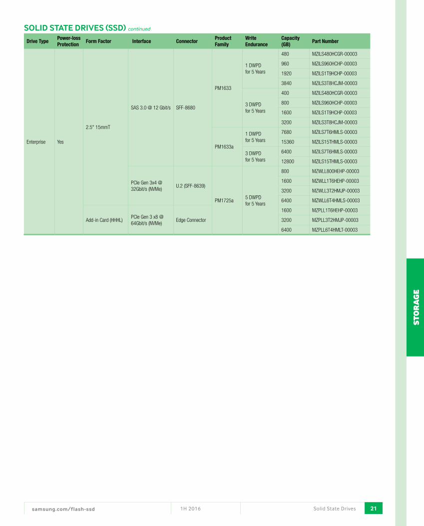
SOLID STATE DRIVES (SSD) continued
Drive TypePower-loss Protection
Form Factor Interface Connector Product Family
WriteEndurance
Capacity (GB)
Part Number
Enterprise Yes
2.5" 15mmT
SAS 3.0 @ 12 Gbit/s SFF-8680
PM1633
1 DWPDfor 5 Years
480 MZILS480HCGR-00003
960 MZILS960HCHP-00003
1920 MZILS1T9HCHP-00003
3840 MZILS3T8HCJM-00003
3 DWPDfor 5 Years
400 MZILS480HCGR-00003
800 MZILS960HCHP-00003
1600 MZILS1T9HCHP-00003
3200 MZILS3T8HCJM-00003
PM1633a
1 DWPDfor 5 Years
7680 MZILS7T6HMLS-00003
15360 MZILS15THMLS-00003
3 DWPDfor 5 Years
6400 MZILS7T6HMLS-00003
12800 MZILS15THMLS-00003
PCIe Gen 3x4 @ 32Gbit/s (NVMe)
U.2 (SFF-8639)
PM1725a5 DWPDfor 5 Years
800 MZWLL800HEHP-00003
1600 MZWLL1T6HEHP-00003
3200 MZWLL3T2HMJP-00003
6400 MZWLL6T4HMLS-00003
Add-in Card (HHHL)PCIe Gen 3 x8 @ 64Gbit/s (NVMe)
Edge Connector
1600 MZPLL1T6HEHP-00003
3200 MZPLL3T2HMJP-00003
6400 MZPLL6T4HMLT-00003

samsungdisplay.com22 1H 2016DID Panel Lineup, Tablets & Monitors
Public Information Display (PID) Product Classification
Why PID instead of TV? COMMERCIAL (PID) CONSUMER (TV)
WARRANTY 18 months to 2 years 90 days to 1 year
RELIABILITY
Public environments
20+ hours daily duty cycle
Variety of temperatures & location
5-8 hour daily duty cycle
Designed for in-home use in controlled environment
In-home living room
PRODUCTION LIFECYCLE 24-36 months 12-15 months
PICTURE QUALITY
Designed to resist image retention
LCD backlight covers a wider color spectrum necessary for PC source integration, giving better picture quality
AGAR coating for public viewing
120Hz / 240Hz for full-motion video
Designed for TV signals
Gloss surface treatment
LOCATION Most models portrait capable Can only be oriented in landscape mode
Product Segmentation
Type Class Warranty BezelSuggested Run Time
Brightness Usage Applications Value Tier
ENB / UNB / SNB
Ultra / Super Narrow Bezel 2 years1.9mm - 5.9mm A-to-A
20+ hours 500-700 nits Heavy Video Walls Premium commercial range
Indoor PID Indoor Commercial Panels 2 years Narrow 20+ hours 600/700 nits Medium Semi-Outdoor Mid-price range
E-Board Value, Large Format 18 months Normal 12 hours 450 nits Daily Indoor, e-Board High-value commercial range
Outdoor PID High Bright, Wide Temp 2 years Normal 20+ hours 2500-5000 nits Heavy Outdoor Premium commercial range
Specialty Value, Large Format 2 years Narrow 20+ hours 500/ 1500 nits Medium specialty
Super Narrow Bezel (SNB)/Ultra Narrow Bezel (UNB)
» UNB: 3.9mm A-to-A» SNB: 5.9mm A-to-A» Video Wall
» Narrow BezelIndoor PID » 700 nits Brightness» 40"/46"/55"/75"
» Landscape OrientationE-Board PID » AGAR Surface Treatment» 55"/70"/82" Edge LED
» High BrightnessOutdoor PID » 110°C Clearing Point» Full High Definition
Product Segmentation
HEAVY USE
LIGHT USE
SNB / UNB Professional Indoor Events Billboard
• Control Room• Simulation
• Scoreboard• Sports Broadcasting
• Dynamic Signage
Indoor PID Entertainment Transportation Communication
• Casino• Theatre• Menu
• Airport• Train/Bus Station
• Conference Room
E-Board PID Commercial Education Hospitality
• Kiosk• Conference Systems
• Interactive FPD • Hotel Signage
Outdoor PID Commercial Education Hospitality
• Kiosk• Conference Systems
• Interactive FPD • Hotel Signage

DIS
PLA
YS
samsungdisplay.com 231H 2016
SAMSUNG DIGITAL INFORMATION DISPLAY (DID) PANEL LINEUP
Category Model SizeModel Resolution
Bezel BacklightBrightness (typical)
Contrast Ratio
Response Time
Frequency MP* Comment
SNB / UNB / ENB
LTI460HN01 (EOL '15.4Q)
46" FHD Super narrow D-LED 700 nits 3,000:1 8ms 60Hz Now 5.9mm Active to Active, LED
LTI460HN09 46" FHD Super narrow D-LED 500 nits 3,000:1 8ms 60Hz Now 5.9mm Active to Active, LED
LTI460HN11 46" FHD Ultra narrow D-LED 500 nits 3,000:1 8ms 60Hz Now 3.9mm Active to Active, LED
LTI460HN12 46" FHD Ultra narrow D-LED 700 nits 3,000:1 8ms 60Hz Now 3.9mm Active to Active, LED
LTI550HN01 (EOL '15.4Q)
55" FHD Super narrow D-LED 700 nits 3,000:1 8ms 60Hz Now 5.9mm Active to Active, LED
LTI550HN08 (EOL '16.2Q)
55" FHD Super narrow D-LED 500 nits 3,000:1 8ms 60Hz Now 5.7mm Active to Active, LED
LTI550HN11-V 55" FHD Ultra narrow D-LED 500 nits 3,000:1 8ms 60Hz Now 3.9mm Active to Active, LED
LTI550HN12-V 55" FHD Ultra narrow D-LED 700 nits 3,000:1 8ms 60Hz Now 3.9mm Active to Active, LED
LTI550HN13-V (Broadcast)
55" FHD Ultra narrow D-LED 700 nits 3,000:1 8ms 60Hz Now 3.9mm Active to Active, LED
LTI550HN14-V (MP '16.2Q)
55" FHDExtreme narrow
D-LED 700 nits 3,000:1 8ms 60Hz Now 1.94mm Active to Active, LED
Indoor PID
LTI400HA10 40" FHD Narrow eLED 700 nits 3,000:1 8ms 60Hz Now eLED, Landscape / Portrait
LTI460HN08 46" FHD Narrow eLED 700 nits 4,000:1 8ms 60Hz Now eLED, Landscape / Portrait
LTI480HN01 48" FHD Narrow Slim eLED 700 nits 4,000:1 8ms 60Hz 16.Q4 Slim eLED,Landscape / Portrait
LTI480HN02 48" FHD Narrow Slim eLED 500 nits 4,000:1 8ms 60Hz 16.Q4 Slim eLED, Landscape / Portrait
LTI550HN06 55" FHD Narrow eLED 700 nits 4,000:1 8ms 60Hz Now eLED, Landscape / Portrait
LTI550HN07 55" FHD Narrow eLED 450 nits 4,000:1 8ms 60Hz Now E-Board; Landscape/Portrait
LTI550FN01 55" UHD Narrow Slim eLED 500 nits 4,000:1 8ms 60Hz 16. Q3 Slim eLED, Landscape / Portrait
LTI750HF02-0 75" FHD Normal D-LED 400 nits 3,500:1 8ms 120Hz Now Landscape / Portrait
LTI750FJ01 75" UHD Normal D-LED 500 nits 5,000:1 8ms 120Hz Now Landscape / Portrait
LTI750FN01 75" UHD Normal eLED 600 nits 4,000:1 8ms 60Hz 16. Q2 eLED Landscape / Portrait
LTI980FN01 98" UHD Normal eLED 500 nits 4,000:1 8ms 60Hz 16. Q2 eLED Landscape / Portrait
E-BoardLTI700HN02 70" FHD Normal eLED 350 nits 4,000:1 8ms 60Hz 16. Q2 E-Board; Landscape mode only
LTI750FN02 75" UHD Normal eLED 350 nits 4,000:1 8ms 60Hz 16. Q3 E-Board; Landscape mode only
Outdoor
LTI460HZ01 46" FHD Narrow D-LED 5,000 nits 4,000:1 8ms 60Hz Now High Bright, Hi Temp LC, 1/4λ Pol.
LTI460HF01-V 46" FHD Narrow D-LED 2,500 nits 3,000:1 8ms 120Hz Now High Bright, Hi Temp LC, 1/4λ Pol.
LTH550HF04-V 55" FHD Narrow D-LED 2,500 nits 3,000:1 8ms 120Hz Now High Bright, Hi Temp LC, 1/4λ Pol.
LTI750HF01-V 75" FHD Narrow D-LED 3,500 nits 3,000:1 8ms 120Hz Now High Bright, Hi Temp LC, 1/4λ Pol.
Specialty
LTI290LN01 29" Half FHD Narrow eLED 500 nits 4,000:1 16ms 60Hz 16. Q2 Stretched, 40"/2, Hi Temp LC
LTI290LN02 29" Half FHD Narrow eLED 700 nits 4,000:1 16ms 60Hz 16. Q3 Stretched, 40"/2, Hi Temp LC
LTI370LN01 37" Half FHD Narrow eLED 700 nits 4,000:1 16ms 60Hz 16. Q2 Stretched, 46"/2, Hi Temp LC
LTI370LN02 37" Half FHD Narrow eLED 1500 nits 4,000:1 16ms 60Hz 16. Q3 Stretched, 46"/2, Hi Temp LC
DID Panel Lineup

samsung.com/semiconductor/sales-network24 1H 2016
Adelsa | www.adetronics.com.mx
PRODUCTS ADDRESS MAIN PHONE FAX
Memory, SLSI, LCD MEXICO Hacienda Corralejo #80, Bosque de Echegaray, Naucalpan, Mexico 53310
52-555-560-5002
GUADALAJARA OFFICE 52-333-122-3054
MONTERREY OFFICE 52-818-214-0011
CD. JUAREZ OFFICE 52-656-613-3517
REYNOSA OFFICE 52-899-922-5540
ATMI Sales | www.atmisales.com
PRODUCTS ADDRESS MAIN PHONE FAX
Memory, LCD OREGON 4900 S.W. Griffith Drive, Suite 253 Beaverton, OR 97005
1-800-898-2446, 503-643-8307
503-643-4364
WASHINGTON 8581 154th Avenue NE Redmond WA 98052
425-869-7636 425-869-9841
Bear VAI Technology | www.bearvai.com
PRODUCTS ADRRESS MAIN PHONE FAX
Memory, SLSI, LCD MAIN OFFICE - BRECKSVILLE, OHIO
6910 Treeline Drive, Unit H Brecksville, OH 44141
440-526-1991 440-526-5426
MAIN OFFICE - INDIANA
11451 Overlook Drive Fishers, IN 46037
440-832-7637 317-845-8650
MICHIGAN 17426 Williow Ridge Drive Northville, MI 48168
440-526-1991 440-526-5426
Core Sales, Inc. | www.coresales.com
PRODUCTS ADDRESS MAIN PHONE FAX
Memory, SLSI, LCD 901 Warrenville Road, Suite 211, Lisle, IL 60532 847-843-8888
Crestone Technology Group | www.crestonegroup.com
PRODUCTS ADDRESS MAIN PHONE FAX
Memory, SLSI, LCD UTAH OFFICE 1578 Trailside Road Farmington, UT 84025
801-245-9752
COLORADO 7108 S. Alton Way, Building L, Suite A Centennial, CO 80112
303-280-7202 720-482-2220
Customer 1st | www.customer1st.com
PRODUCTS ADDRESS MAIN PHONE FAX
Memory, SLSI, LCD MINNESOTA 2950 Metro Drive, Suite 101Bloomington, MN 55425
952-851-7909 952-851-7907
KANSAS 2111 E. Crossroad Lane, #202Olathe, KS 66062
Contacts
Feel free to contact your local distributor or sales representative with any Samsung sales inquiries.
DID Panel Lineup, Tablets & Monitors
For all product information please visit: www.samsung.com/us/samsungsemiconductor

25
CO
NTA
CTS
samsung.com/semiconductor/sales-network 1H 2016 Contacts
InTELaTECH | www.intelatech.com
PRODUCTS ADDRESS MAIN PHONE FAX
Memory, SLSI 5225 Orbitor Drive, Suite 2, Mississauga, ONT Canada L4W 4Y8 905-629-0082 905-624-6909905-629-1795905-629-8910
21 Concourse Gate, Suite 12, Ottawa, ONT Canada K2E 7S4 905-629-0082 613-221-9160
I-Squared Incorporated | www.isquared.com
PRODUCTS ADDRESS MAIN PHONE FAX
Memory, SLSI, LCD 2635 N. 1st Street, Suite 128, San Jose, CA 95134 408-988-3400 408-988-2079
1250 B Street, Petaluma, CA 94952 707-773-3108
Neptune Electronics (necco) | www.neccoelect.com
PRODUCTS ADDRESS MAIN PHONE FAX
Memory, SLSI, LCD 11 Oval Drive, Suite 169, Islandia, NY 11749 631-234-2525 631-234-2707
New Elpis, Inc. | www.newelpis.com
PRODUCTS ADDRESS MAIN PHONE FAX
LCD 165 Dundas St. W., Suite 702, Mississauga, ONT, Canada L4Z 2H6 905-275-3516 905-275-4109
New Tech Solutions
PRODUCTS ADDRESS MAIN PHONE FAX
Memory, SLSI, LCD 26 Ray Avenue, Burlington, MA 01803 781-229-8888 781-229-1614
Rep One Associates, Inc. | www.repone.com
PRODUCTS ADDRESS MAIN PHONE FAX
Memory, SLSI, LCD ALABAMA 303 Williams Avenue, Suite 1011Huntsville, AL 35801
256-539-7371 256-533-4509
GEORGIA 3000 Langford Road, Bldg 300Norcross, GA 30071
770-209-9242678-591-6753
770-209-9245
Tech Coast Sales | www.tc-sales.com
PRODUCTS ADDRESS MAIN PHONE EMAIL
Memory, SLSI, LCD 23121 Verdugo Drive, Suite 101, Laguna Hills, CA 92653 949-305-6869 [email protected]
West Associates | www.westassociates.com
PRODUCTS ADDRESS MAIN PHONE FAX
Memory, SLSI, LCD AUSTIN / SAN ANTONIO
4100 Duval Road, Building 1, Suite 102, Austin, TX 78759
512-343-1199 512-343-1922
DALLAS / OKLAHOMA / ARKANSAS
2745 Dallas Parkway, Suite 460, Plano, TX 75093
972-680-2800 972-699-0330
HOUSTON / VALLEY / LOUISIANA
24624 Interstate 45 North, Suite 200, Spring, TX 77386
512-343-1199 512-343-1922

samsung.com/semiconductor/sales-network26 1H 201626
Notes

27
CO
NTA
CTS
samsung.com/semiconductor/sales-network 1H 2016 27
Notes
Disclaimer: The information in this publication has been carefully checked and is believed to be accurate at the time of publication. Samsung assumes no responsibility, however, for possible errors or omissions, or for any consequences resulting from the use of the information contained herein. Samsung reserves the right to make changes in its products or product specifications with the intent to improve function or design at any time and without notice and is not required to update this documentation to reflect such changes. This publication does not convey to a purchaser of semiconductor devices described herein any license under the patent rights of Samsung or others. Samsung makes no warranty, representation, or guarantee regarding the suitability of its products for any particular purpose, nor does Samsung assume any liability arising out of the application or use of any product or circuit and specifically disclaims any and all liability, including without limitation any consequential or incidental damages.
Copyright 2016. Samsung and Samsung Semiconductor, Inc. are registered trademarks of Samsung Electronics, Co., Ltd. Ultrabooks is a trademark of Intel Corporation. All other names and brands may be claimed as the property of others. The appearance of all products, dates, figures, diagrams and tables are subject to change at any time, without notice.
BR-16-ALL-001 | Printed 3/16
Samsung Semiconductor, Inc. 3655 North First Street San Jose, CA 95134-1713
samsung.com/us/oem-solutions