probing the molecular conformation of self-assembled
TRANSCRIPT

Instructions for use
Title Probing the Molecular Conformation of Self-Assembled Monolayers at Metal/Semiconductor Interfaces by VibrationalSum Frequency Generation Spectroscopy
Author(s) Asanuma, Hidehiko; Noguchi, Hidenori; Huang, Yifan; Uosaki, Kohei; Yu, Hua-Zhong
Citation Journal of Physical Chemistry C, 113(50), 21139-21146https://doi.org/10.1021/jp9062675
Issue Date 2009-12-17
Doc URL http://hdl.handle.net/2115/50209
Type article
File Information JPCC113-50_21139-21146.pdf
Hokkaido University Collection of Scholarly and Academic Papers : HUSCAP
Probing the Molecular Conformation of Self-Assembled Monolayers at Metal/Semiconductor Interfaces by Vibrational Sum Frequency Generation Spectroscopy
Hidehiko Asanuma,† Hidenori Noguchi,‡ Yifan Huang,† Kohei Uosaki,*,‡ and Hua-Zhong Yu*,†
Department of Chemistry, Simon Fraser UniVersity, Burnaby, British Columbia V5A 1S6, Canada, and DiVisionof Chemistry, Graduate School of Science, Hokkaido UniVersity, Sapporo 060-0180, Japan
ReceiVed: July 3, 2009; ReVised Manuscript ReceiVed: October 15, 2009
The conformation of self-assembled monolayers (SAMs) buried at metal-semiconductor interfaces plays acrucial role in the functioning of the molecular junctions thus formed. We have studied by vibrational sumfrequency generation (SFG) spectroscopy the influence of deposited gold films on the molecular orientationof a series of n-alkyl monolayers that are covalently bonded to silicon(111) via Si-C linkages (≡Si-CnH2n+1,n ) 10, 12, 14, and 18). The SFG spectra indicate that the gold contacts (overlayers) introduce significantgauche defects within the initially highly oriented alkyl chains. The methyl tilt angles of the buried n-alkylmonolayers depend on the gold deposition method (vacuum evaporation vs sputtering) and the alkyl chainlength. These observations are supported by solid-state electrical measurements.
1. Introduction
Sum frequency generation (SFG) spectroscopy is based on asecond-order nonlinear optical effect in which photons aregenerated at a frequency equal to the sum of the frequencies ofthe two incident beams.1-4 It is an interface-sensitive techniquebecause the effect is forbidden in media exhibiting inversionsymmetry; at a surface or interface such inversion symmetry isnecessarily broken. By using visible and tunable infrared inputbeams, SFG can detect specific vibrations at a buried interfaceat the time resolution of the laser source. In addition, thepolarization combinations of SFG, visible and IR beams canbe powerful diagnostic tools for the determination of molecularorientations: the ssp (s-polarized SFG, s-polarized visible, andp-polarized IR) combination detects vibrational modes withdipole moments perpendicular to the interface, the sps and psscombinations are sensitive to dipole moments parallel to thesurface, and the ppp combination responds to both perpendicularand parallel components. The main advantage of SFG spec-troscopy, compared with the conventional infrared techniques(FT-IR and Raman), is its capability to reveal the conformation,lateral order, and orientation of surface-bound molecules.5,6 Forexample, Shen and co-workers have determined that themolecular orientations of pentadecanoic acids at a water surfacedepend on their surface densities; the monolayer undergoes atransition from the highly disordered “liquid expanded” to the“liquid condensed” phase, for which the alkyl chains areextended toward the air and oriented nearly normal to the watersurface.1
SFG spectroscopy has also been adapted to the study ofmolecular conformations of self-assembled monolayers (SAMs)formed on various substrates.7-16 Two decades ago, Guyot-Sinnest et al. reported that octadecyltrichlorosilane (OTS)monolayers on silica are oriented normal to the surface.8 Hineset al. have shown that alkanethiolate SAMs on gold and silverare relatively more ordered than those prepared on platinum;
however, the latter can be “straightened” by applying electro-chemical potentials.9 Yeganeh et al. discovered that SFG spectraof alkanethiolate monolayers on a gold(111) surface exhibit anazimuthal angle dependence and attributed this behavior to thebinding pattern of the molecules.16 Liu et al. studied the role ofwater during the adsorption of OTS on a fused silica surfaceby monitoring conformational changes of the monolayers.11
Recently, Ye et al. examined the orientation of water moleculesat the surface of OTS monolayers on quartz under neutral andacidic conditions.14,15 Nishi et al. found that the ratio betweenCH3 symmetric and asymmetric vibration modes of alkanethi-olate SAMs on gold depends on whether the number of carbonsis odd or even; this may be due to the difference in the tiltdirection of the terminal methyl groups.13
The miniaturization of electronic devices in the past decadehas increased the demand for fabricating nanoscale structures,in which organic molecules act as either passive (i.e., tunnelingjunctions, rectifiers) or active components (i.e., switches,transistors, and logic gates).17 Organic molecules are generallyassembled into monolayers whose orientation and conformationplay a crucial role in the functioning of the molecular junctionsthus formed. Several spectroscopic studies of SAMs at metal/metal or metal/semiconductor interfaces have been reportedrecently.18-23 While Jun and Zhu developed an attenuated totalreflection (ATR) method to probe buried molecular interfacesby IR spectroscopy,20 p-polarized backside reflection absorptioninfrared spectroscopy (pb-RAIRS) has been adapted by Richteret al. to the study of the interactions between deposited metalcontacts and organic monolayers on silicon surfaces.21 Theseinvestigations typically rely on observed peak broadening,frequency shifts, and intensity variations. Hacker et al. havereported the complete disappearance of methylene bands fromthe IR spectrum of an octadecyl monolayer on silicon upon thedeposition of a 5 nm gold film.22
In this work, we explore vibrational SFG spectroscopy as anew technique to probe the molecular orientation of self-assembled monolayers at metal/semiconductor interfaces. Thesamples were prepared by depositing gold contacts onto alkylmonolayers covalently bonded to silicon surfaces.23,24 Weexamined not only the effect of the alkyl chain length but also
* To whom correspondence should be addressed. E-mail: [email protected](H.-Z.Y.), [email protected] (K.U.).
† Simon Fraser University.‡ Hokkaido University.
J. Phys. Chem. C 2009, 113, 21139–21146 21139
10.1021/jp9062675 2009 American Chemical SocietyPublished on Web 11/17/2009

the influence of the coating method (thermal evaporation vssputtering deposition) on the electrical properties of the Au/alkyl monolayer/Si junctions formed. Besides recording changesof various vibrational band frequencies and intensities due tothe CH3 and CH2 groups, we were able to monitor the Au-CHinteractions directly by combining SFG with ATR-IR spec-troscopic studies.
2. Experimental Section
2.1. Materials. All chemicals were ACS reagent grade andused as received unless otherwise mentioned. Deionized water(>18.3 Ω · cm) was used throughout the experiments. 1-Decene(94%), 1-dodecene (95%), 1-tetradecene (92%), 1-octadecene(90%), and 1,1,1,-trichloroethane (99.5%) were obtained fromAldrich; tetrahydrofuran (THF), sulfuric acid (96%), andhydrogen peroxide (30%) were purchased from Wako Chemi-cals. Ammonium fluoride (40%) was from Morita ChemicalIndustries. 1-Decene (94%), 1-dodecene (95%), 1-tetradecene(92%), and 1-octadecene (90%) were distilled from sodiumunder reduced pressure (20-30 Torr), followed by freeze-thawcycles under vacuum/nitrogen.
2.2. Surface Preparation. Silicon(111) wafers (0.5-5.0Ω · cm, n-type, Virginia Semiconductor Inc.) were cut toappropriate size (1.5 × 2 cm) and then cleaned in a “piranha”solution (3:1 mixture of H2SO4 and H2O2) for 30 min at 90 °C.CAUTION: “Piranha” solution must be handled with extremecare as it reacts Violently with organic materials. After copiousrinsing with deionized water, the silicon wafers were etchedwith deoxygenated NH4F (40% aqueous solution) to removenative oxide and obtain hydrogen-terminated silicon (≡Si-H).The fresh ≡Si-H samples were then introduced under argoninto Schlenk tubes containing 2-3 mL of deoxygenated neat1-alkenes and heated to 160 °C for 4 h. Thus, modified siliconsamples (≡Si-CnH2n+1, n ) 10, 12, 14, and 18; abbreviated asC10, C12, C14, and C18, respectively) were cleaned with THF,trifluororoacetic acid solution in THF (1%), and 1,1,1-trichlo-roethane sequentially and blow-dried with N2 gas.
Gold deposition on freshly prepared silicon samples wasperformed via thermal evaporation or sputtering coating.Thermal evaporation was carried out in a vacuum evaporationapparatus (Ulvac, EBH-6). The chamber pressure was loweredto the base pressure of 10-6 Torr using a diffusion pump; gold(99.99%) was then deposited at a rate of 0.1 nm/s until it reachedthe film thickness of 10 nm (measured by a calibrated quartzcrystal oscillator). Gold sputtering was carried out with a JoelJFC-1200 sputtering coater in an argon-purged chamber underreduced pressure (∼2.0 × 10⁻² Torr). The filament current waskept at approximately 15 mA until the desired film thickness(∼10 nm) was reached. The size of gold contacts was controlledby using an aluminum mask with nine holes (3 mm diameter).
2.3. SFG System. A picosecond Nd:YAG laser (PL2143B,Ekspla) was used to pump an optical parametric generation/optical parametric amplification/difference frequency generation(OPG/OPA/DFG) system to produce tunable infrared radiation(2.3-8.5 µm).14,15,25 The second harmonic output of the YAG(yttrium-aluminum-garnet) laser at 532 nm was used as thevisible light source. At the incident angle of 70° for visible andof 50° for infrared light, two beams were loosely focused ontothe sample. The [21j1j] direction of Si(111) samples was set inthe plane of the incident beams during measurements. Theproduced SFG signal was filtered through irises and a mono-chromator (Oriel Instruments, MS257) and amplified by aphotomultiplier tube (PMT, Hamamatsu, R3896). All measure-ments were carried out with p-polarized SFG, visible and IR
beams (abbreviated ppp). The SFG signal was normalized tothe intensities of the visible and infrared light; all experimentswere carried out in air at room temperature (22 ( 2 °C).
The following formulas were used to fit the SFG intensity(ISFG)
ISFG(ωSFG ) ωIR + ωVIS) ∝ |eff(2):E(ωIR)E(ωVIS)|2
(1)
eff(2) ) |NR
(2) |eiφn + ∑ An
ωIR - ωn + iΓn(2)
where eff(2) and NR
(2) are the effective second-order nonlinearsusceptibilities of the resonant and nonresonant component,respectively, φn is the phase angle between the resonant andnonresonant component, and An and Γn are the amplitude andthe homogeneous width of the surface vibration mode (n)corresponding to the frequency ωn, respectively. On the basisof the above equations, a nonlinear least-squares routine wasdeveloped in our laboratory to fit the SFG spcetra.14,15 Thequality of the fit is judged by r2 values that were at least 0.900.Specifically, for each vibrational band, the fitting parameterswere An, ωIR, and Γn, while the NR
(2) and φn were kept constantfor the entire spectrum. Another parameter (a constant for flatand a linear term for uneven baselines) was added to adjust thebaseline, and this term does not influence the spectral features.Peak intensity ratios were calculated from the amplitudes ofindividual vibration modes (An). All uncertainties were derivedfrom the spectra of at least three samples.
2.4. Electrical Measurements. The solid-state electricalmeasurements were carried out with an Autolab electrochemicalanalyzer (model PGSTAT 30, Eco Chemie BV, The Nether-lands). All measurements were performed in a Faraday cage.The contact to the gold pad was made by lowering a tungstenprobe with a homemade micropositioning system. The current-voltage (I-V) curves were recorded from +0.5 to -0.5 V at ascan rate of 0.05 V/s. The Mott-Schottky plots (C-2 vs V) wereacquired by scanning the potential from +0.1 to -1.5 V at afrequency of 100 kHz.
2.5. Other Measurements. Wetting measurements werecarried out with an AST Optima contact angle system at ambientconditions (18-23 °C, 30-35% relative humidity) using ahorizontal light beam to illuminate a 2.0 µL water droplet.Ellipsometric measurements were performed with a Uviselspectroscopic ellipsometer (Horiba Jobin Yvon) over the rangeof 300-700 nm at an incident angle of 70°. All reportedexperimental uncertainties are derived from at least three spotsfrom three independent samples.
3. Results and Discussion
Previous FT-IR spectroscopic studies of self-assembledmonolayers (SAMs) at metal/metal (semiconductor) interfaceshave provided valuable information regarding metal-moleculeinteractions, based on the attenuation of certain vibrationalmodes, peak broadening, or position shifts. For example, Boeret al. proposed that the decrease of the IR peak intensity of the-CH3 groups of 1-hexadecanethiolate monolayers on gold isdue to the Au/Al and CH3 interactions;18 Jun and Zhu havesuggested that the peak broadening observed for metal/OTS/silicon interfaces is due to monolayer disordering and the peakattenuation due to the cleavage of C-H bonds.20 Theseobservations may not be simply explained because the dipolesof molecules can be “suppressed” by the metal overlayers, andthe roughness of the metal layer may induce scattering of theinfrared beam at the metal/molecule interface.26 There are cases
21140 J. Phys. Chem. C, Vol. 113, No. 50, 2009 Asanuma et al.

where new bands arise upon the deposition of metal atoms ontop of the organic monolayer; Richter et al. assigned the newpeak at ∼2825 cm-1 from the metal/OTS/Si system tomethylene-metal interactions.21 Nevertheless, the above-mentioned spectral features are not easily distinguishable as theyare typically broad, weak, and sometimes obscured. SFGspectroscopy can provide additional or complementary informa-tion to these IR studies, as it is intrinsically sensitive to theinterfacial molecular conformation and exhibits submonolayersensitivity.27
3.1. Alkyl Monolayers on Silicon. The Si-C-bonded alkylmonolayers were first examined by SFG spectroscopy prior tothe metal deposition (Figure 1). All spectra exhibited featuresthatcorrespondtodenselypackedandwell-orientedmonolayers.10,12,25
Specifically, contributions from methylene (CH2) stretchingmodes were negligible, and the spectral features were dominatedby the contributions from the methyl (CH3) groups: methylsymmetric stretch (r+) at ∼2878 cm-1, Fermi resonance (FR)
between r+ and the CH bending overtone at ∼2940 cm-1, andthe CH3 asymmetric stretch (r-) at ∼2964 cm-1. These are thefeatures of well-ordered and closely packed molecular mono-layers that have the alkyl chains in all-trans configurations. Theellipsometric thickness and the wetting measurements sum-marized in Table 1 support the above interpretation. Themonotonic thickness increase of the C10 to C18 monolayerswith the alkyl chain length is in good agreement with valuescalculated for an average alkyl chain tilt angle of 35° (corre-sponding to a CH3 tilt angle of ∼70°) (Table 1). The static watercontact angles were around 110° for all four monolayer systems,comparable to previous reports for well-packed (intrinsicallyhydrophobic) alkyl monolayers.24,28-30 ATR-IR studies provideadditional evidence (e.g., strong CH2 asymmetric and symmetricstretching bands) for the high quality of these monolayers (seethe Supporting Information).
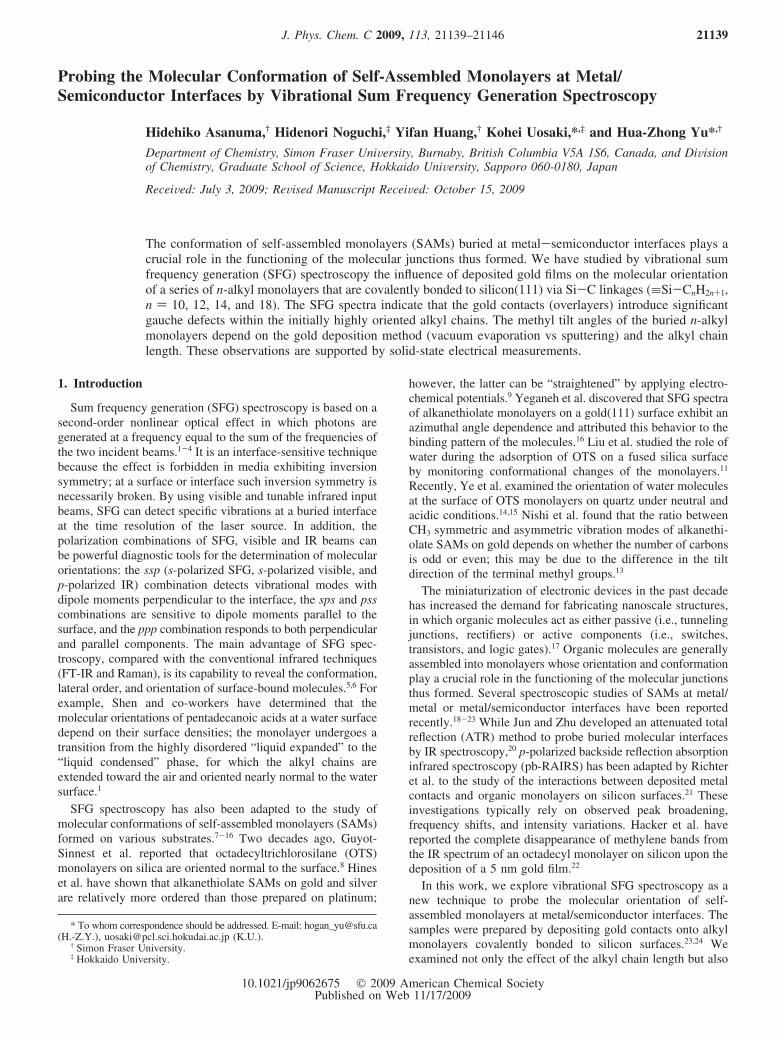
3.2. Alkyl Monolayers at Gold/Silicon Interfaces. Figures2 and 3 show the SFG spectra of the C10, C12, C14, and C18monolayers on silicon with deposited gold overlayers. Thesamples were prepared by thermal evaporation and sputteringdeposition. In contrast to Figure 1, the vibrational bands appearas downward peaks due to a phase difference between thenonresonant background (contributed largely from the goldoverlayer) and the resonant signal,31,32 which is also related tothe laser configuration9 and has been observed for SFG spectraof alkanethiol SAMs on gold.9,32 In general, upon gold deposi-tion, strong CH2 symmetric (d+) and asymmetric (d-) peaksappear at ∼2850 and ∼2920 cm-1. The methylene groups ofwell-ordered alkyl chains are positioned in a symmetric manner,yet when gauche defects are introduced, such symmetry isbroken and the SFG signal arises. Therefore, these new bandsindicate that trans-gauche defects in the alkyl chain backbonesare introduced upon metal deposition.25,33 Independent of thealkyl chain lengths, both thermal evaporation and sputteringdeposition of gold contacts disrupt the molecular conformationof the SAMs significantly, as evidenced by the substantialcontributions of the methylene bands (d+ and d-). As shownby the deconvoluted peaks (Figures 2 and 3), methylenecontributions relative to methyl peaks are observed to be strongerfor samples prepared via sputtering than for those prepared bythermal evaporation; that is, the sputtering method is moredestructive. Another important feature of these SFG spectra isthe appearance of a new band at ∼2900 cm-1. Although d+
Fermi resonance and several other factors prevent a definiteassignment of this band, we have cautiously assigned it tomethylene (CH2) groups that are interacting with gold, specif-ically to the CH bonds that are in the proximity of, but not indirect contact with, gold atoms.34,35 This means that, upon metaldeposition, some regions of the alkyl chains are not directly incontact with gold. It has been suggested that gold will
Figure 1. SFG spectra of (a) ≡Si-(CH2)9CH3 (C10), (b)≡Si-(CH2)11CH3 (C12), (c) ≡Si-(CH2)13CH3 (C14), and (d)≡Si-(CH2)17CH3 (C18). The solid lines (in black) show the best fitsto the experimental data (open circles) based on eqs 1 and 2; thedeconvoluted peaks are shown in red at the bottom (see the main textfor details).
TABLE 1: Thickness and Wetting Measurements of AlkylMonolayers on Silicon
sample H2O contact angle/degree dexp/Å dcalc/Åa
≡Si-(CH2)9CH3 (C10) 109 ( 2 12.8 ( 1.0 11.4≡Si-(CH2)11CH3 (C12) 108 ( 3 14.0 ( 1.2 13.5≡Si-(CH2)13CH3 (C14) 109 ( 2 15.4 ( 1.1 15.7≡Si-(CH2)17CH3 (C18) 106 ( 2 20.4 ( 1.3 20.0
a The predicted monolayer thickness was calculated from theequation d ) 1.86 + 1.30(n - 1)cos θ, where d is the thickness, nis the number of carbons in the alkyl chain, and θ is the anglebetween the molecule axis and the surface normal. An average tiltangle, θ ) 35°, was used to calculate the thickness of each alkylmonolayer.
SAMs at Metal/Semiconductor Interfaces J. Phys. Chem. C, Vol. 113, No. 50, 2009 21141
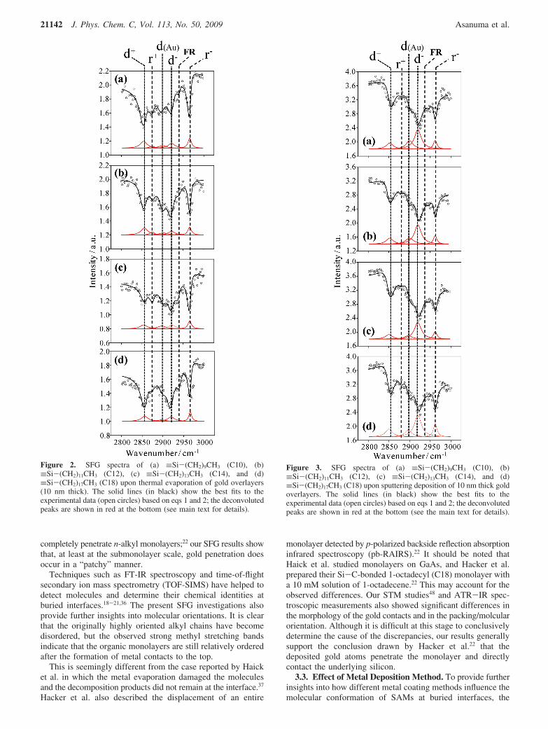
completely penetrate n-alkyl monolayers;22 our SFG results showthat, at least at the submonolayer scale, gold penetration doesoccur in a “patchy” manner.
Techniques such as FT-IR spectroscopy and time-of-flightsecondary ion mass spectrometry (TOF-SIMS) have helped todetect molecules and determine their chemical identities atburied interfaces.18-21,36 The present SFG investigations alsoprovide further insights into molecular orientations. It is clearthat the originally highly oriented alkyl chains have becomedisordered, but the observed strong methyl stretching bandsindicate that the organic monolayers are still relatively orderedafter the formation of metal contacts to the top.
This is seemingly different from the case reported by Haicket al. in which the metal evaporation damaged the moleculesand the decomposition products did not remain at the interface.37
Hacker et al. also described the displacement of an entire
monolayer detected by p-polarized backside reflection absorptioninfrared spectroscopy (pb-RAIRS).22 It should be noted thatHaick et al. studied monolayers on GaAs, and Hacker et al.prepared their Si-C-bonded 1-octadecyl (C18) monolayer witha 10 mM solution of 1-octadecene.22 This may account for theobserved differences. Our STM studies48 and ATR-IR spec-troscopic measurements also showed significant differences inthe morphology of the gold contacts and in the packing/molcularorientation. Although it is difficult at this stage to conclusivelydetermine the cause of the discrepancies, our results generallysupport the conclusion drawn by Hacker et al.22 that thedeposited gold atoms penetrate the monolayer and directlycontact the underlying silicon.
3.3. Effect of Metal Deposition Method. To provide furtherinsights into how different metal coating methods influence themolecular conformation of SAMs at buried interfaces, the
Figure 2. SFG spectra of (a) ≡Si-(CH2)9CH3 (C10), (b)≡Si-(CH2)11CH3 (C12), (c) ≡Si-(CH2)13CH3 (C14), and (d)≡Si-(CH2)17CH3 (C18) upon thermal evaporation of gold overlayers(10 nm thick). The solid lines (in black) show the best fits to theexperimental data (open circles) based on eqs 1 and 2; the deconvolutedpeaks are shown in red at the bottom (see main text for details).
Figure 3. SFG spectra of (a) ≡Si-(CH2)9CH3 (C10), (b)≡Si-(CH2)11CH3 (C12), (c) ≡Si-(CH2)13CH3 (C14), and (d)≡Si-(CH2)17CH3 (C18) upon sputtering deposition of 10 nm thick goldoverlayers. The solid lines (in black) show the best fits to theexperimental data (open circles) based on eqs 1 and 2; the deconvolutedpeaks are shown in red at the bottom (see the main text for details).
21142 J. Phys. Chem. C, Vol. 113, No. 50, 2009 Asanuma et al.

intensity ratio of the methyl symmetric and asymmetric stretchesAq(r-)/Aq(r+) was used to estimate the average tilt angle usingthe following equation:38-40
|Aq(r-)
Aq(r+) | )|caa
aac×
(2Fzzz - Fxxz)(cos θ - cos3 θ)
(Fzzz +12
Fxxz(1 + r))cos θ - Fzzz - Fxxz(1 - r)cos3 θ |(3)
In eq 3, θ is the angle between the main axis of the methylgroup and the surface normal; Fzzz and Fxxz are combinations ofthe Fresnel factors for the SFG, visible, and IR beams; is thehyperpolarizability; and r is the ccc/aac ratio (equal to 0.25).The ratio caa/aac has a value of 4.21.41 This model can beapplied to the C3V symmetry for the methyl groups under theassumption that the zzz and xxz susceptibility elements dominatethe SFG signal (for gold/silicon interfaces).42
Fzzz, Fxxz > >Fxzx, Fzxx (4)
Therefore, the tilt angle determination using eq 3 is notapplicable to the silicon substrate; it is only valid after depositionof gold that significantly enhances the electric field of the zcomponent. Rather than a particular or an averaged tilt angle,it is more realistic to estimate the range for each monolayersystem. Generally, a Gaussian distribution can be assumed tomodel the methyl orientation angles (see the SupportingInformation).43-45
f(θ) ) Cexp[-(θ - θ0)/2σ2)] (5)
In eq 5, θ0 is the mean orientation angle, C is a normalizationconstant, and σ is the root-mean-square width. For a directcomparison, thus obtained methyl tilt angles for alkyl mono-layers at gold/silicon interfaces are summarized in Table 2.
The average tilt angles of the alkyl chains in alkyl monolayerson silicon have been reported to be 35-40°,12,24,42 whichcorresponds to methyl tilt angles of 70-75°. This means thatthe alkyl chains become less tilted; that is, they “stand up” fromthe surface upon metal deposition (Table 2). The absolute tiltangles are difficult to determine due to gauche defects and thewide range of possible orientations. Focusing on the differencesbetween the two gold deposition methods, as shown in Table2, the methyl tilt angles for the samples prepared via thermalevaporation are much smaller than those prepared by sputtering
deposition and their values range from 18° to 28°, independentof the different alkyl chain lengths. On the other hand, the tiltangles of methyl groups for samples prepared via sputteringdeposition exhibit chain-length dependence: their tilt becomessmaller as the chain length increases from C10 to C18. Suchremarkable variations indicate that different structural changesare induced during the deposition of gold overlayers (bysputtering vs thermal evaporation) on identically preparedn-alkyl monolayers on silicon.
In the case of thermal evaporation, the solid metal melts andevaporates in the crucible mounted at the bottom of a vacuumchamber. The metal vapor consequently condenses and depositsonto the sample, inducing a certain level of damage to theorganic monolayer because of the energy released from of thegradually condensing atoms.46 The observed identical, but small,tilt angle of alkyl monolayers on silicon buried underneath thegold contacts may be due to thermal expansion during the goldevaporation process, a known phenomenon.42,47 This means thatirrespective of the chain length, all monolayers stand upvertically on the substrate upon metal deposition; that is, themethyl tilt angles become much smaller in comparison tothe values prior to metal deposition. The thermal radiation ofthe boiling gold source (>3000 K) makes the molecules moremobile, as evidenced by the new CH2 vibration band (Scheme1).
In sputtering deposition, gold atoms are “dislocated” fromthe source (target) as struck by the high-energy ions generatedby magnetron-assisted DC plasma. The “emitted” high-energy,neutral metal atoms travel toward the sample situated on theopposite side of the chamber. Sputtering is considered to bemore energetic than thermal evaporation, as the kinetic energyof ions is transferred to the ejected metal atoms. Sputtered atomsejected from the target have a wide energy distribution, typicallytens of electronvolts, which is much higher than the thermal
TABLE 2: Estimated Methyl Tilt Angles (θ) of AlkylMonolayers at Gold/Silicon Interfaces; the Range Was Basedon the Assumption of Gaussian Distributions (See Text forDetails)
thermal evaporation sputtering
sample A(r-)/A(r+) tilt angles A(r-)/A(r+) tilt angles
≡Si-(CH2)9CH3 (C10) 2.6 ( 0.3 18-28° 5.7 ( 0.7 62-80°≡Si-(CH2)11CH3 (C12) 2.6 ( 0.4 18-28° 4.4 ( 0.4 46-66°≡Si-(CH2)13CH3 (C14) 2.5 ( 0.2 18-28° 4.1 ( 0.6 41-49°≡Si-(CH2)17CH3 (C18) 2.4 ( 0.3 18-28° 3.3 ( 0.7 33-36°
SCHEME 1: Hypothetical View of Monolayer-Metal Interactions during Gold Deposition via (a) Thermal Evaporationand (b) Sputtering Deposition
SAMs at Metal/Semiconductor Interfaces J. Phys. Chem. C, Vol. 113, No. 50, 2009 21143
energy of condensing gold atoms (∼0.27 eV). Thermal expan-sion of the monolayer will be minimized in this case becausethe source is kept cold; however, the high kinetic energies allowthe metal atoms to penetrate the monolayers more readily thanin the thermal evaporation process (Scheme 1, b1). The differenttilt angles upon sputtering gold on top of alkyl monolayers onsilicon indicate that the monolayers respond to the bombardmentwith high-energy gold atoms differently. Although a short-chainmonolayer (i.e., C10) will simply maintain its original tilt angle,the longer alkyl chains may be reoriented upon metal penetra-tion. As the gaps between molecules are occupied slowly bymetal atoms, the molecules gradually stand up. The affinity ofmethylene groups for gold atoms has been demonstratedpreviously;35 thus, longer alkyl chains will limit the mobilityof gold atoms within the monolayer.
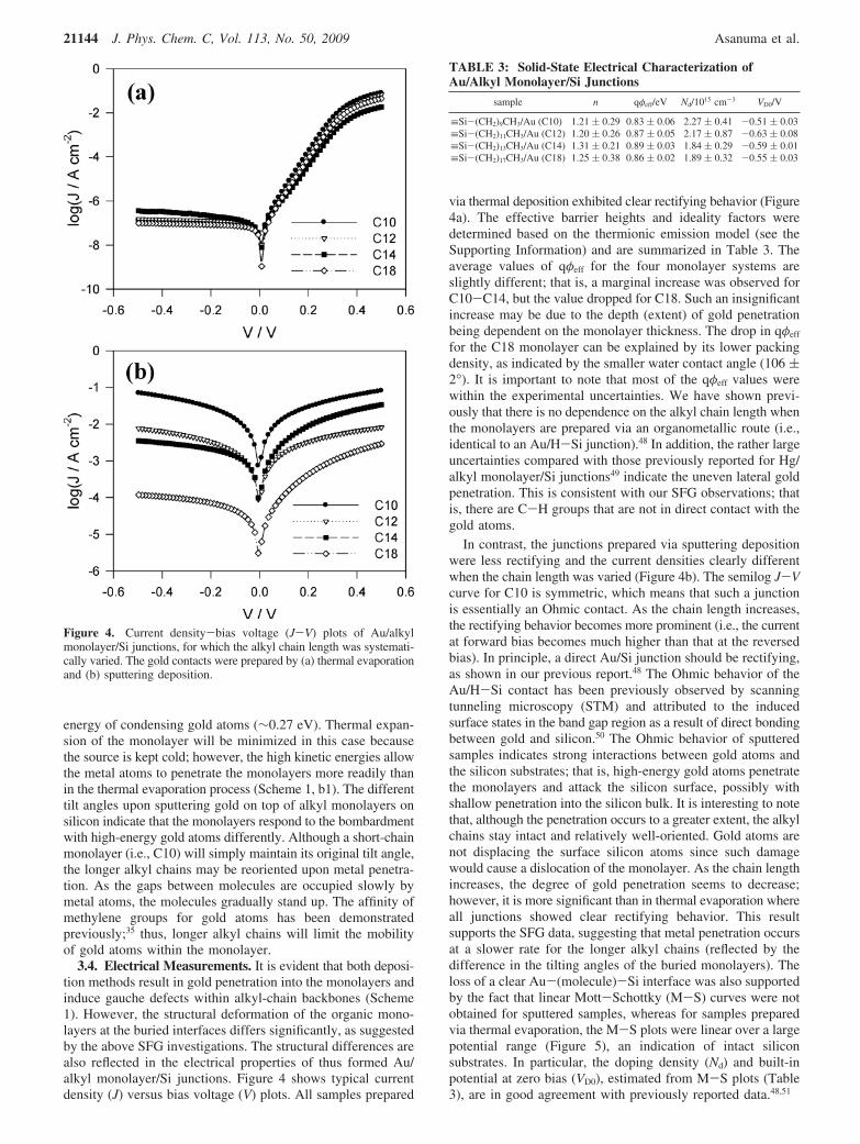
3.4. Electrical Measurements. It is evident that both deposi-tion methods result in gold penetration into the monolayers andinduce gauche defects within alkyl-chain backbones (Scheme1). However, the structural deformation of the organic mono-layers at the buried interfaces differs significantly, as suggestedby the above SFG investigations. The structural differences arealso reflected in the electrical properties of thus formed Au/alkyl monolayer/Si junctions. Figure 4 shows typical currentdensity (J) versus bias voltage (V) plots. All samples prepared
via thermal deposition exhibited clear rectifying behavior (Figure4a). The effective barrier heights and ideality factors weredetermined based on the thermionic emission model (see theSupporting Information) and are summarized in Table 3. Theaverage values of qφeff for the four monolayer systems areslightly different; that is, a marginal increase was observed forC10-C14, but the value dropped for C18. Such an insignificantincrease may be due to the depth (extent) of gold penetrationbeing dependent on the monolayer thickness. The drop in qφeff
for the C18 monolayer can be explained by its lower packingdensity, as indicated by the smaller water contact angle (106 (2°). It is important to note that most of the qφeff values werewithin the experimental uncertainties. We have shown previ-ously that there is no dependence on the alkyl chain length whenthe monolayers are prepared via an organometallic route (i.e.,identical to an Au/H-Si junction).48 In addition, the rather largeuncertainties compared with those previously reported for Hg/alkyl monolayer/Si junctions49 indicate the uneven lateral goldpenetration. This is consistent with our SFG observations; thatis, there are C-H groups that are not in direct contact with thegold atoms.
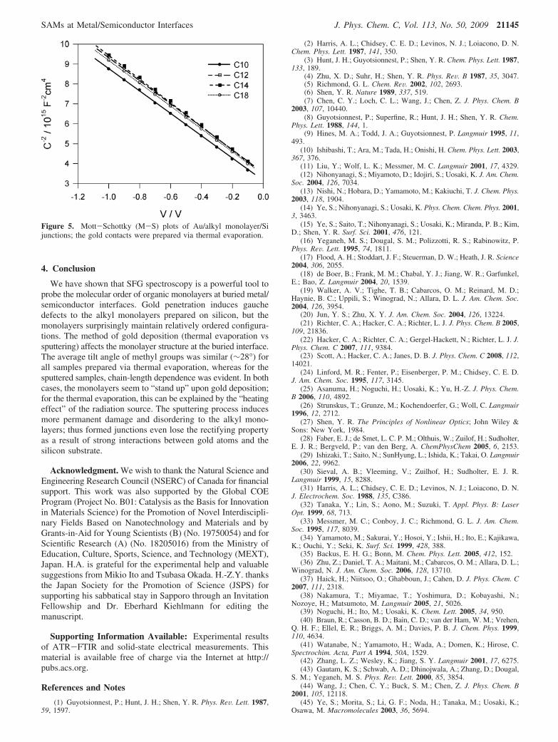
In contrast, the junctions prepared via sputtering depositionwere less rectifying and the current densities clearly differentwhen the chain length was varied (Figure 4b). The semilog J-Vcurve for C10 is symmetric, which means that such a junctionis essentially an Ohmic contact. As the chain length increases,the rectifying behavior becomes more prominent (i.e., the currentat forward bias becomes much higher than that at the reversedbias). In principle, a direct Au/Si junction should be rectifying,as shown in our previous report.48 The Ohmic behavior of theAu/H-Si contact has been previously observed by scanningtunneling microscopy (STM) and attributed to the inducedsurface states in the band gap region as a result of direct bondingbetween gold and silicon.50 The Ohmic behavior of sputteredsamples indicates strong interactions between gold atoms andthe silicon substrates; that is, high-energy gold atoms penetratethe monolayers and attack the silicon surface, possibly withshallow penetration into the silicon bulk. It is interesting to notethat, although the penetration occurs to a greater extent, the alkylchains stay intact and relatively well-oriented. Gold atoms arenot displacing the surface silicon atoms since such damagewould cause a dislocation of the monolayer. As the chain lengthincreases, the degree of gold penetration seems to decrease;however, it is more significant than in thermal evaporation whereall junctions showed clear rectifying behavior. This resultsupports the SFG data, suggesting that metal penetration occursat a slower rate for the longer alkyl chains (reflected by thedifference in the tilting angles of the buried monolayers). Theloss of a clear Au-(molecule)-Si interface was also supportedby the fact that linear Mott-Schottky (M-S) curves were notobtained for sputtered samples, whereas for samples preparedvia thermal evaporation, the M-S plots were linear over a largepotential range (Figure 5), an indication of intact siliconsubstrates. In particular, the doping density (Nd) and built-inpotential at zero bias (VD0), estimated from M-S plots (Table3), are in good agreement with previously reported data.48,51
Figure 4. Current density-bias voltage (J-V) plots of Au/alkylmonolayer/Si junctions, for which the alkyl chain length was systemati-cally varied. The gold contacts were prepared by (a) thermal evaporationand (b) sputtering deposition.
TABLE 3: Solid-State Electrical Characterization ofAu/Alkyl Monolayer/Si Junctions
sample n qφeff/eV Nd/1015 cm-3 VD0/V
≡Si-(CH2)9CH3/Au (C10) 1.21 ( 0.29 0.83 ( 0.06 2.27 ( 0.41 -0.51 ( 0.03≡Si-(CH2)11CH3/Au (C12) 1.20 ( 0.26 0.87 ( 0.05 2.17 ( 0.87 -0.63 ( 0.08≡Si-(CH2)13CH3/Au (C14) 1.31 ( 0.21 0.89 ( 0.03 1.84 ( 0.29 -0.59 ( 0.01≡Si-(CH2)17CH3/Au (C18) 1.25 ( 0.38 0.86 ( 0.02 1.89 ( 0.32 -0.55 ( 0.03
21144 J. Phys. Chem. C, Vol. 113, No. 50, 2009 Asanuma et al.
4. Conclusion
We have shown that SFG spectroscopy is a powerful tool toprobe the molecular order of organic monolayers at buried metal/semiconductor interfaces. Gold penetration induces gauchedefects to the alkyl monolayers prepared on silicon, but themonolayers surprisingly maintain relatively ordered configura-tions. The method of gold deposition (thermal evaporation vssputtering) affects the monolayer structure at the buried interface.The average tilt angle of methyl groups was similar (∼28°) forall samples prepared via thermal evaporation, whereas for thesputtered samples, chain-length dependence was evident. In bothcases, the monolayers seem to “stand up” upon gold deposition;for the thermal evaporation, this can be explained by the “heatingeffect” of the radiation source. The sputtering process inducesmore permanent damage and disordering to the alkyl mono-layers; thus formed junctions even lose the rectifying propertyas a result of strong interactions between gold atoms and thesilicon substrate.
Acknowledgment. We wish to thank the Natural Science andEngineering Research Council (NSERC) of Canada for financialsupport. This work was also supported by the Global COEProgram (Project No. B01: Catalysis as the Basis for Innovationin Materials Science) for the Promotion of Novel Interdiscipli-nary Fields Based on Nanotechnology and Materials and byGrants-in-Aid for Young Scientists (B) (No. 19750054) and forScientific Research (A) (No. 18205016) from the Ministry ofEducation, Culture, Sports, Science, and Technology (MEXT),Japan. H.A. is grateful for the experimental help and valuablesuggestions from Mikio Ito and Tsubasa Okada. H.-Z.Y. thanksthe Japan Society for the Promotion of Science (JSPS) forsupporting his sabbatical stay in Sapporo through an InvitationFellowship and Dr. Eberhard Kiehlmann for editing themanuscript.
Supporting Information Available: Experimental resultsof ATR-FTIR and solid-state electrical measurements. Thismaterial is available free of charge via the Internet at http://pubs.acs.org.
References and Notes
(1) Guyotsionnest, P.; Hunt, J. H.; Shen, Y. R. Phys. ReV. Lett. 1987,59, 1597.
(2) Harris, A. L.; Chidsey, C. E. D.; Levinos, N. J.; Loiacono, D. N.Chem. Phys. Lett. 1987, 141, 350.
(3) Hunt, J. H.; Guyotsionnest, P.; Shen, Y. R. Chem. Phys. Lett. 1987,133, 189.
(4) Zhu, X. D.; Suhr, H.; Shen, Y. R. Phys. ReV. B 1987, 35, 3047.(5) Richmond, G. L. Chem. ReV. 2002, 102, 2693.(6) Shen, Y. R. Nature 1989, 337, 519.(7) Chen, C. Y.; Loch, C. L.; Wang, J.; Chen, Z. J. Phys. Chem. B
2003, 107, 10440.(8) Guyotsionnest, P.; Superfine, R.; Hunt, J. H.; Shen, Y. R. Chem.
Phys. Lett. 1988, 144, 1.(9) Hines, M. A.; Todd, J. A.; Guyotsionnest, P. Langmuir 1995, 11,
493.(10) Ishibashi, T.; Ara, M.; Tada, H.; Onishi, H. Chem. Phys. Lett. 2003,
367, 376.(11) Liu, Y.; Wolf, L. K.; Messmer, M. C. Langmuir 2001, 17, 4329.(12) Nihonyanagi, S.; Miyamoto, D.; Idojiri, S.; Uosaki, K. J. Am. Chem.
Soc. 2004, 126, 7034.(13) Nishi, N.; Hobara, D.; Yamamoto, M.; Kakiuchi, T. J. Chem. Phys.
2003, 118, 1904.(14) Ye, S.; Nihonyanagi, S.; Uosaki, K. Phys. Chem. Chem. Phys. 2001,
3, 3463.(15) Ye, S.; Saito, T.; Nihonyanagi, S.; Uosaki, K.; Miranda, P. B.; Kim,
D.; Shen, Y. R. Surf. Sci. 2001, 476, 121.(16) Yeganeh, M. S.; Dougal, S. M.; Polizzotti, R. S.; Rabinowitz, P.
Phys. ReV. Lett. 1995, 74, 1811.(17) Flood, A. H.; Stoddart, J. F.; Steuerman, D. W.; Heath, J. R. Science
2004, 306, 2055.(18) de Boer, B.; Frank, M. M.; Chabal, Y. J.; Jiang, W. R.; Garfunkel,
E.; Bao, Z. Langmuir 2004, 20, 1539.(19) Walker, A. V.; Tighe, T. B.; Cabarcos, O. M.; Reinard, M. D.;
Haynie, B. C.; Uppili, S.; Winograd, N.; Allara, D. L. J. Am. Chem. Soc.2004, 126, 3954.
(20) Jun, Y. S.; Zhu, X. Y. J. Am. Chem. Soc. 2004, 126, 13224.(21) Richter, C. A.; Hacker, C. A.; Richter, L. J. J. Phys. Chem. B 2005,
109, 21836.(22) Hacker, C. A.; Richter, C. A.; Gergel-Hackett, N.; Richter, L. J. J.
Phys. Chem. C 2007, 111, 9384.(23) Scott, A.; Hacker, C. A.; Janes, D. B. J. Phys. Chem. C 2008, 112,
14021.(24) Linford, M. R.; Fenter, P.; Eisenberger, P. M.; Chidsey, C. E. D.
J. Am. Chem. Soc. 1995, 117, 3145.(25) Asanuma, H.; Noguchi, H.; Uosaki, K.; Yu, H.-Z. J. Phys. Chem.
B 2006, 110, 4892.(26) Strunskus, T.; Grunze, M.; Kochendoerfer, G.; Woll, C. Langmuir
1996, 12, 2712.(27) Shen, Y. R. The Principles of Nonlinear Optics; John Wiley &
Sons: New York, 1984.(28) Faber, E. J.; de Smet, L. C. P. M.; Olthuis, W.; Zuilof, H.; Sudholter,
E. J. R.; Bergveld, P.; van den Berg, A. ChemPhysChem 2005, 6, 2153.(29) Ishizaki, T.; Saito, N.; SunHyung, L.; Ishida, K.; Takai, O. Langmuir
2006, 22, 9962.(30) Sieval, A. B.; Vleeming, V.; Zuilhof, H.; Sudholter, E. J. R.
Langmuir 1999, 15, 8288.(31) Harris, A. L.; Chidsey, C. E. D.; Levinos, N. J.; Loiacono, D. N.
J. Electrochem. Soc. 1988, 135, C386.(32) Tanaka, Y.; Lin, S.; Aono, M.; Suzuki, T. Appl. Phys. B: Laser
Opt. 1999, 68, 713.(33) Messmer, M. C.; Conboy, J. C.; Richmond, G. L. J. Am. Chem.
Soc. 1995, 117, 8039.(34) Yamamoto, M.; Sakurai, Y.; Hosoi, Y.; Ishii, H.; Ito, E.; Kajikawa,
K.; Ouchi, Y.; Seki, K. Surf. Sci. 1999, 428, 388.(35) Backus, E. H. G.; Bonn, M. Chem. Phys. Lett. 2005, 412, 152.(36) Zhu, Z.; Daniel, T. A.; Maitani, M.; Cabarcos, O. M.; Allara, D. L.;
Winograd, N. J. Am. Chem. Soc. 2006, 128, 13710.(37) Haick, H.; Niitsoo, O.; Ghabboun, J.; Cahen, D. J. Phys. Chem. C
2007, 111, 2318.(38) Nakamura, T.; Miyamae, T.; Yoshimura, D.; Kobayashi, N.;
Nozoye, H.; Matsumoto, M. Langmuir 2005, 21, 5026.(39) Noguchi, H.; Ito, M.; Uosaki, K. Chem. Lett. 2005, 34, 950.(40) Braun, R.; Casson, B. D.; Bain, C. D.; van der Ham, W. M.; Vrehen,
Q. H. F.; Ellel, E. R.; Briggs, A. M.; Davies, P. B. J. Chem. Phys. 1999,110, 4634.
(41) Watanabe, N.; Yamamoto, H.; Wada, A.; Domen, K.; Hirose, C.Spectrochim. Acta, Part A 1994, 50A, 1529.
(42) Zhang, L. Z.; Wesley, K.; Jiang, S. Y. Langmuir 2001, 17, 6275.(43) Gautam, K. S.; Schwab, A. D.; Dhinojwala, A.; Zhang, D.; Dougal,
S. M.; Yeganeh, M. S. Phys. ReV. Lett. 2000, 85, 3854.(44) Wang, J.; Chen, C. Y.; Buck, S. M.; Chen, Z. J. Phys. Chem. B
2001, 105, 12118.(45) Ye, S.; Morita, S.; Li, G. F.; Noda, H.; Tanaka, M.; Uosaki, K.;
Osawa, M. Macromolecules 2003, 36, 5694.
Figure 5. Mott-Schottky (M-S) plots of Au/alkyl monolayer/Sijunctions; the gold contacts were prepared via thermal evaporation.
SAMs at Metal/Semiconductor Interfaces J. Phys. Chem. C, Vol. 113, No. 50, 2009 21145

(46) Haick, H.; Cahen, D. Prog. Surf. Sci. 2008, 83, 217–261.(47) Salomon, A.; Shpaisman, H.; Seitz, O.; Boecking, T.; Cahen, D. J.
Phys. Chem. C 2008, 112, 4169.(48) Kuikka, M. A.; Li, W. J.; Kavanagh, K. L.; Yu, H.-Z. J. Phys.
Chem. C 2008, 112, 9081.(49) Liu, Y.-J.; Yu, H.-Z. ChemPhysChem 2002, 3, 799.
(50) Gheber, L. A.; Hershfinkel, M.; Gorodetsky, G.; Volterra, V. ThinSolid Films 1998, 320, 228.
(51) Asanuma, H.; Bishop, E. M.; Yu, H.-Z. Electrochim. Acta 2007,52, 2913.
JP9062675
21146 J. Phys. Chem. C, Vol. 113, No. 50, 2009 Asanuma et al.