printing and profiling fine feature devices apex 2003
TRANSCRIPT
© Cookson Electronics, 2003
Printing and Profiling Fine Feature Devices
Chrys Shea Bruce Moloznik
Cookson Electronics Assembly Materials Jersey City, New Jersey
David Hemmelgarn
Cookson Electronics Equipment Franklin, Massachusetts
Abstract To characterize the paste printing process, both the individual aspects of the process and the interactions between the aspects must be understood. The main aspects of the printing process are paste, stencil, printer and board. Each can be singularly optimized to obtain desired results, but the system as a whole should be optimized to yield the most robust process. The profiling process can often be overshadowed by the importance of proper printing. It is in the reflow process where the interconnections are permanently formed, and great care should be taken to ensure that these connections are formed under the proper thermal conditions. Profiling methods, profile types, and resulting reflow recipes are also discussed. Introduction Electronic device miniaturization continues to drive assemblers to refine their solder printing process for surface mount assemblies. The advent of 0201’s and .5mm CSP’s demands yet another level of refinement, and many assemblers are struggling to understand the capability of their printing process to repeatably produce paste deposits as small as 0.25mm (0.010”) in diameter. The process of depositing solder paste on a circuit board is critical to the success of fine feature assembly. Historically, higher yields have been achieved by optimizing individual aspects of the printing process. Examples of individual aspect optimization include modifying aperture geometries, board surface finishes, or paste properties. Unfortunately, modifying one aspect of the process can often create new issues in other parts of the process. To successfully make the next jump in technology, the entire printing system must be approached as a complete process. The interactions within the system must be well understood in order to gain advancement without any concessions.
Likewise, the reflow process must be optimized to produce reliable joints, but at a reasonable cost. Because most fine feature devices are currently used in small consumer electronics, high throughput rates are desired to support the economics of high volume assembly. Reflow profiles must be carefully generated to guarantee reliable solder joints at the lowest possible cost. The four, main components of the fine feature printing process that will be discussed are paste, stencil, printer, and board. The factors affecting reflow reliability and cost are profiling techniques, profile types, and throughput rates. Paste Solder paste plays a critical role in electronics altogether. Its deposition on the board is the first key step in the assembly process. It must form solder joints that provide sound electrical and mechanical connections. The chemical residues that remain on the finished assembly must be benign in order to ensure long-term reliability for the end product. The broad range of requirements on solder paste often leads to tradeoffs between specific performance

© Cookson Electronics, 2003
characteristics in order to achieve robust process windows and maintain reliability. The size of the solder powder particles is a critical factor in a solder paste’s ability to print small features repeatably. The electronics assembly industry has developed and relied upon “rules of thumb” for years to assist in the implementation of new technologies. One of the generally accepted rules cites that the diameter of the largest solder sphere can be no larger than ¼ of the smallest aperture span on the stencil. The implication of this rule is that mechanical interference due to the size of the particles, relative to the dimension of the aperture, becomes a critical factor in fine feature applications. The resulting inference is that performance of traditional solder paste (Type 3) can be significantly challenged in the areas of print definition and volume consistency. Table 1 illustrates the powder classification methods based on solder sphere sizes.
Table 1
Solder Powder Classification based on particle size (in microns)
Table 2 compares aperture spans to sphere diameters. It is clear that as apertures get smaller, the anecdotal 4:1 limit is approached, and in an extreme case, reached. Paste manufacturers have two options to address this potential issue. One approach is to use smaller particle sizes in the paste product (Type 4 or Type 5 powder); the other is to modify the rheological properties of the paste flux. Device Type/ Aperture
Span
Sphere Dia (mm)
Typical Max / Absolute Max
Ratio
.6mm CSP/ .3mm (12mil)
.045mm .05mm
6.7:1 6:1
.5mm CSP/ .25mm (10mil)
.045mm .05mm
5.5:1 5:1
0201 footprint A/ .36mm (14mil)
.045mm .05mm
8:1 7.2:1
0201 footprint B/ .18mm (9.1mil)
.045mm .05mm
4:1 3.6:1
Table 2
Ratio of Aperture Span to Sphere Size The obvious solution of using a smaller solder particle size has important quality and economic implications. Quality implications arise because of the potential to include more unwanted oxides in the solder paste itself. Excessive oxides can cause random solder balls to form because they inhibit the coalescence of the molten solder during the reflow process. Excessive oxides can also hamper wetting to components and pads. Although solder powder is manufactured under inert conditions, opportunities for the surfaces of the spheres to oxidize occur during handling, blending, storage, and the thermal excursion of reflow. Maximizing the ratio of the spheres’ volume to their surface area by using a larger particle size minimizes the opportunity to include the unwanted oxides that can cause solderability problems. The economic implications of using Type 4 or Type 5 powders are based on the principles of supply and demand. Type 3 powder is used in more than 95% of today's solder pastes. To meet this demand, global solder powder manufacturers have designed their processes to produce Type 3 powder and optimized them to maximize Type 3 output. If demand for Type 4 were to rapidly increase while supply is low, the user would certainly encounter higher costs associated with its availability. The use of universally available Type 3 powder offers a variety of important advantages over Type 4, but requires more science and engineering to be incorporated into the paste itself. The engineering of advanced rheological paste fluxes addresses both the potential increased reflow defect rate and possible higher
TYPE
None Larger Than
Less than 1% Larger Than
80% Minimum Between
10% Maximum Less Than
1 160 150 150-75 20 2 80 75 75-45 20 3 50 45 45-25 20 4 40 38 38-20 20 5 30 25 25-15 15 6 20 15 15-5 5

© Cookson Electronics, 2003
costs related to finer mesh powders. A variety of formulation techniques can be employed to achieve these results. The techniques themselves are beyond the scope of this discussion, but the results of their application are quantifiable. A designed experiment was executed to determine defect rates of 0201 components that were assembled using advanced flux technology and Type 3 powder. The study was performed by an independent laboratory that compared the results to the same tests performed on standard pastes.1 Over 50,000 placements were analyzed for each paste product. Two pad sizes and two pad spacings were used for all experiments. Defect types included tombstone, solder bridge, insufficient solder, and post-reflow skew. Figures 1 though 3 depict the defect modes.
Figure 1 0201 Tombstone Defect
Figure 2
0201 Solder Bridge Defect
Figure 3 0201 Post Reflow Skew
Table 3 shows the defect rates based on pad design and gap between pads. It is clear that smaller gaps generated more defects, and interesting to note that smaller pads created less defects. The overall defect pareto is shown in Figure 4.
Pad Gap Defects
# Comp’s
DPMO
Small
Small
3 19440 154
Small
Large
1 19440 51
Large
Small
2 19440 103
Large
Large
1 19440 51
Total
7 77760 90
Table 3
Assembly Defect Rates for 0201 Components

© Cookson Electronics, 2003
Tombstone14%
Solder Bridge28%
Insufficient Solder30%
Skew28%
Figure 4 Assembly Defect Pareto Analysis for 0201
Components The comparative results between the advanced technology flux paste and competitive Type 3 and Type 4 paste materials are shown in Figure 5.
90
116
154
201
0
50
100
150
200
250
AdvancedTech. Flux
Material A Material B Material C
Defe
cts
Per M
illio
n O
ppor
tunt
ies
Figure 5
Comparative Results of Four Solder Pastes in 0201 Assembly Defect Rates
The study showed an average 43% reduction in defects rates on 0201 components when advanced flux technology was employed. The technique of overcoming the challenges of fine feature printing with chemical flux formulation and universally available Type 3 Powder is a very desirable solution. Resolving the concerns of finer mesh powders by engineering the flux chemistry eliminates many quality and cost implications for the assembler.
Stencil Another popular “rule of thumb” in stencil printing is the aspect ratio of the stencil aperture. The aspect ratio offers guidelines that relate the height of the deposit (or stencil thickness) to the minimum aperture span for effective solder paste release. This rule was developed with fine pitch printing in mind. In this case, the term “fine pitch” refers to leaded devices with lead spacing of 25mils or less that have rectangular pads. For these cases, the aspect ratio remains an effective rule. “Fine feature” printing involves devices of similar pitch, but with much smaller pads that have square or round geometries. The aspect ratio fails to adequately predict paste release in these situations. For fine feature devices, the rule of area ratio must be applied. The area ratio is defined as the surface area of the pad underneath the aperture opening divided by the surface area of the aperture walls. As a stencil and board are separated, the forces holding the solder paste to the pad must overcome the forces holding the solder paste in the stencil in order to affect a repeatable, predictable release. To guarantee repeatable release, the Surface Area Ratio should be greater than 0.6. Table 4 contains surface area ratios for circular and square aperture geometries on stencils with foil thicknesses of 4 and 5 mils. Pad Size Area Ratio Pad Shape (mils) 5mil foil 4mil foil Circle 6 0.30 0.38 Circle 7 0.35 0.44 Circle 8 0.40 0.50 Circle 9 0.45 0.56 Circle 10 0.50 0.63 Circle 11 0.55 0.69 Circle 12 0.60 0.75 Circle 14 0.70 0.88 Circle 16 0.80 1.00 Circle 18 0.90 1.13 Circle 20 1.00 1.25 Square 6 0.30 0.38 Square 7 0.35 0.44 Square 8 0.40 0.50 Square 9 0.45 0.56
© Cookson Electronics, 2003
Square 10 0.50 0.63 Square 11 0.55 0.69 Square 12 0.60 0.75 Square 14 0.70 0.88 Square 16 0.80 1.00 Square 18 0.90 1.13 Square 20 1.00 1.25
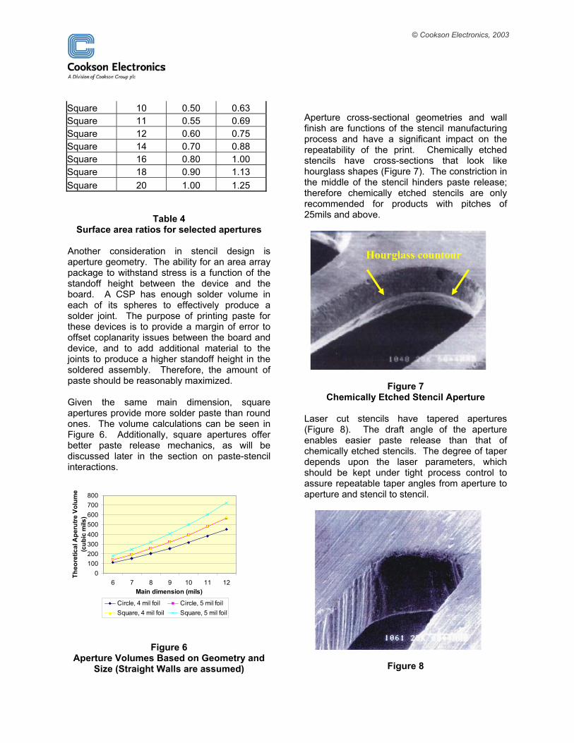
Table 4 Surface area ratios for selected apertures
Another consideration in stencil design is aperture geometry. The ability for an area array package to withstand stress is a function of the standoff height between the device and the board. A CSP has enough solder volume in each of its spheres to effectively produce a solder joint. The purpose of printing paste for these devices is to provide a margin of error to offset coplanarity issues between the board and device, and to add additional material to the joints to produce a higher standoff height in the soldered assembly. Therefore, the amount of paste should be reasonably maximized. Given the same main dimension, square apertures provide more solder paste than round ones. The volume calculations can be seen in Figure 6. Additionally, square apertures offer better paste release mechanics, as will be discussed later in the section on paste-stencil interactions.
0100200300400500600700800
6 7 8 9 10 11 12Main dimension (mils)
Theo
retic
al A
peru
tre V
olum
e (c
ubic
mils
)
Circle, 4 mil foil Circle, 5 mil foilSquare, 4 mil foil Square, 5 mil foil
Figure 6 Aperture Volumes Based on Geometry and
Size (Straight Walls are assumed)
Aperture cross-sectional geometries and wall finish are functions of the stencil manufacturing process and have a significant impact on the repeatability of the print. Chemically etched stencils have cross-sections that look like hourglass shapes (Figure 7). The constriction in the middle of the stencil hinders paste release; therefore chemically etched stencils are only recommended for products with pitches of 25mils and above.
Figure 7 Chemically Etched Stencil Aperture
Laser cut stencils have tapered apertures (Figure 8). The draft angle of the aperture enables easier paste release than that of chemically etched stencils. The degree of taper depends upon the laser parameters, which should be kept under tight process control to assure repeatable taper angles from aperture to aperture and stencil to stencil.
Figure 8
Hourglass countour

© Cookson Electronics, 2003
Laser Cut & Electropolished Aperture Electroformed stencils (Figure 9) provide two advantages for paste release. The unique manufacturing process produces very smooth walls. Also, the surface tension of the electroformed alloys are lower than that of stainless steel foils, which also aids in release. Electroformed stencils are recommended for devices with pitches smaller than 0.5mm (20mils).
Figure 9
Electroformed Aperture The taper angle of stencil apertures is another age-old “rule of thumb” that is currently being studied. When laser cut stencils were introduced, the taper naturally formed by the manufacturing process provided superior paste release when compared to the hourglass contour of chemically etched apertures. Because the angle of the taper is a function of the laser cutting parameters, engineers and scientists began experimenting to find the optimum angle. The results of these studies are very interesting: higher draft angles may provide better paste release, but as the taper angle is increased, the volume of the aperture is decreased. Angles can only be increased to a certain point when the drawbacks of lower volumes outweigh the benefits of better release. Reverse tapers2 are being investigated as an emerging stencil technology. Reversing a taper on an aperture means the trapezoidal cross-section is smaller at the board interface and larger at the squeegee interface. Reverse tapers have been shown to deposit more paste, in a more prismatic form, with less cold slump
upon release. Their smaller cross-sectional area at the board interface improves gasketing, thereby limiting the opportunity for smears or wet bridges. Initial studies have shown that reverse tapers provide higher paste deposit volumes, but may exhibit more variation in the volumes they deposit. Studies are continuing on the reverse taper, and more information on their viability as a technology that can enable fine feature printing should be available in the upcoming year. Printer The printer itself is a key component of the process as it is the automation on which the assembler relies to apply paste to circuit boards. Some of the critical factors in the equipment include alignment capability, pressure balance and paste delivery method. Alignment is critical to achieving high quality solder deposits. To accommodate fine features, printers should be able to repeatably align the stencil to the board within 0.025mm (1mil). On coarser pitch devices, stencil apertures are typically cropped to accommodate positional inaccuracies between the board and printer while assuring good gasketing between the stencil and board. For fine feature devices, however, solder volumes are critical, and aperture cropping needs to be minimized. Therefore, good gasketing must be achieved through good alignment of the stencil with a high degree of positional accuracy. In squeegee print systems, the balance of pressure along the length of the squeegee and between the back and front strokes plays an important part in print repeatability. The forces that drive solder paste into apertures are the result of squeegee speed, angle, and pressure. Although the speed and angle remain constant in most printers, the balance of pressure across the squeegee blade can vary if not properly balanced. This situation creates uneven forces across the squeegee, and different print volumes across the width of the circuit board. It is highly recommended that a precision, balanced print head be utilized for printing fine feature devices with squeegee systems. The final factor unique to the printer is the paste delivery system. Two general types of systems
© Cookson Electronics, 2003
are available: the traditional squeegee, and the newer direct pressure systems. Direct pressure systems involve closed chambers filled with solder paste that are charged to a specific pressure. The pressure is maintained via closed-loop feedback control that updates 40 times per second. The forces directing the solder paste into the stencil apertures are much more consistent across the width of the print and along the length of the stroke. Although pump systems may not be required to achieve good, quality fine feature prints, they add an extra degree of control to the printing process. Board Circuit board design and construction play a considerable role in print yields. To be printable, a board must be “gasketable.” The term gasketing refers to a tight fit between the board and stencil. Any “leaks” between the two can allow paste to be forced into areas where it is not intended to be deposited. Poor gasketing can be the root cause of paste smears, solder bridges, and solder balls. Although gasketing is a multi-variable function of board properties, printer alignment, stencil accuracy and board support, the greatest impact to gasketability can be attributed to the circuit board construction itself. The most obvious impact is that of the board’s surface finish. Flat, planar surfaces are critical to achieve good gasketing and crisp print definition. Hot Air Solder Leveled (HASL) pads have a domed topography, which make gasketing difficult. Flatter surfaces, like those coated with Organic Solderability Preservatives (OSP) provide much better gasketing. Alternatives to OSP that offer similar advantages in surface topography are Electroless Nickel-Immersion Gold, Immersion Silver, and Immersion Tin. It is strongly recommended that one of these HASL alternatives be utilized when assembling fine feature devices. Surface finish is not the only element of board design that impacts the printability of a circuit card. The methods by which the pads are defined is also critical. For most devices, pads are defined by their copper edge, and solder mask is relieved outside the perimeter of the pad
by approximately 2-3mils. However, for fine feature devices, it is sometimes preferable to define the pad with solder mask. In this scenario, the copper pad is slightly oversized, and its solderable surface is defined by an opening in the mask, which overlaps the copper by 2-3mils inside its perimeter. Several fine feature studies have shown that SMD pads generally have higher print volumes than NSMD pads3. This is because the thickness of the soldermask adds an extra amount of volume to the print area. In some cases, such as a CSP, this is considered a benefit, as the extra solder volume will increase reliability with very little opportunity to create a defect. In other cases, such as 0201’s, it may be considered a detriment, as the extra paste may contribute to the formation of mid-chip solder balls when using traditional 0201 apertures. Pad definition methods should be considered when generating stencil apertures for fine feature devices. A third factor that affects the printability of a circuit board is warp. Generally speaking, the mechanics of the printer can overcome a moderate amount of warp in the board during the print process if the proper tooling is in place. Warpage above the printing plane is pressed out by the stencil and print head; warpage below the printing plane must be addressed by support tooling. Even the smallest unsupported areas can cause gasket breaches and poor print quality. In addition to printing issues, board warp can also affect alignment and placement accuracy, so it is wise to minimize the board’s propensity to warp at the design stage. This can be achieved by balancing the distribution of copper in the board, and using laminate materials with higher glass transition temperatures (Tg) and higher thermal degradation temperatures (Td). Typically, the specification of more robust materials adds little or no additional cost to the board itself and eliminates a multitude of assembly issues downstream. Interactions It is nearly impossible to discuss individual main effects of the printing process’ components without discussing their interactions, as the components all come together in the printer to
© Cookson Electronics, 2003
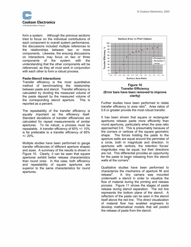
form a system. Although the previous sections tried to focus on the individual contributions of each component to overall system performance, the discussions included multiple references to the relationships between two or more components. Likewise, the ensuing discussions on interactions may focus on two or three components of the system, with the understanding that the other components will be referenced, as they all must work in conjunction with each other to form a robust process. Paste-Stencil Interactions Transfer efficiency is the most quantitative method of benchmarking the relationship between paste and stencil. Transfer efficiency is calculated by dividing the measured volume of the paste deposit by the measured volume of the corresponding stencil aperture. This is reported as a percent. The repeatability of the transfer efficiency is equally important as the efficiency itself. Standard deviations of transfer efficiencies are calculated for repeat measurements of similar apertures. To be robust, a process must be repeatable. A transfer efficiency of 60% +/- 10% is far preferable to a transfer efficiency of 65% +/- 20%. Multiple studies have been performed to gauge transfer efficiencies of different aperture shapes and sizes. A summary of the results is shown in Figure 10. Clearly, it can be seen that square apertures exhibit better release characteristics than round ones. In this case, both efficiency and repeatability of square apertures are superior to the same characteristics for round apertures.
Figure 10
Transfer Efficiency (Error bars have been removed to improve
clarity) Further studies have been performed to relate transfer efficiency to area ratio4. Area ratios of 0.6 or greater provide the most robust transfer. It has been shown that square or rectangular apertures release paste more efficiently than round apertures, particularly when the area ratio approached 0.6. This is presumably because of the corners or vertices of the square geometric shape. The forces holding the paste to the aperture walls are equal around the perimeter of a circle, both in magnitude and direction. In apertures with vertices, the retention forces’ magnitudes may be equal, but their directions are not. This differential provides an opportunity for the paste to begin releasing from the stencil walls at the corners5. Qualitative studies have been performed to characterize the mechanics of aperture fill and release6. A tiny camera was mounted underneath a stencil in order to visualize the flow of material during the printing and release process. Figure 11 shows the stages of paste release during stencil separation. The red line represents the bottom plane of the stencil. A reflection of the paste can be seen in the stencil itself above the red line. This direct visualization of material flow has enabled engineers to develop mathematical models that will predict the release of paste from the stencil.

© Cookson Electronics, 2003
Figure 11 Real Time Visualization of Paste Release
Mechanics The models have been validated with experimental data, and are now enabling engineers to develop processes based on hard data and characterized components. Board-Stencil Interactions The greatest interaction between the board and the stencil is the alignment of the two. One might assume that this is purely a function of the printer itself, but that is not the case. Stencils and boards are both manufactured with tolerances. The printer locates fiducials, calculates the best fit between the components, and positions the stencil accordingly, within its own tolerance range. The positional repeatability of a maintained and calibrated printer is less than 1mil at 6 Sigma levels. The positional repeatability of a stencil manufactured on a properly calibrated and maintained laser machine is less than 1mil at 6 Sigma. The effect of the machines involved in the process are relatively small. The largest factor in alignment is the tolerance of the circuit board itself. A study of the positional accuracy of boards and stencils7 revealed that it is not uncommon for circuit cards to have features located as far as 3mils from nominal. Adding the 1mil tolerance of stencils and the 1mil tolerance of printers, the
paste deposit can shift to 50% off of a 10mil pad. In cases where multiple fine feature devices are distributed around the circuit card, it may be advantageous to map the positional accuracy of the circuit card and incorporate compensating factors in the stencil design. Separation is the next largest factor in the board-stencil interaction. Separation speeds and profiles are critical to achieving crisp print definition. A separation speed that is far too fast will cause “bounce back” of the stencil, ruining the print8. A separation speed that is relatively too fast will cause the paste in the lower part of the aperture to release, but paste in the upper part of the aperture can remain bound to the aperture walls. Recall that the board’s pad pulling forces must overcome the stencil’s wall retention forces in order to affect good release. But solder paste is a thixotropic fluid that “thins” down when shear forces are applied. If the separation is too fast, the opposing forces create shearing forces within the paste that cause the bricks to pull apart, with some paste sticking to the board and some sticking in the aperture. Studies have found that small vibrations during the separation phase of printing aids in the release process. It is theorized that the small vibrations induce shear thinning at the paste-stencil wall interface, aiding in the paste’s release. To accommodate this release mechanism, some printers now have programmable separation profiles in addition to programmable separation speeds. The profile can be programmed with combinations of movement and pauses, and movement may be in either direction of the Z-axis. Because these movements are servo-controlled and extend for no more than 10mils of travel, they have the ability to improve transfer efficiency without negatively impacting cycle time. Separation profiles can be pre-programmed by the equipment manufacturer, or customized by the process engineer. Gasketing between the stencil and the board is somewhat dependent upon alignment, in that gross misalignment will create gasketing issues, but the biggest factors that affect gasketing can be attributed to the board itself.

© Cookson Electronics, 2003
Printer-Board Interaction One of the largest overall factors in successful printing is support. Board support tooling was briefly discussed earlier in terms of its ability to help flatten warped boards, but it is absolutely critical to a successful process, regardless of board condition. There is a multitude of options available to achieve good support. They include programmable pin placement systems, edge clamps, custom-molded worknests, custom-designed metal vacuum plates, and newly introduced gel tooling. The type of tooling required to achieve adequate support is very dependent upon the product being assembled. The criticality of good support increases as board thickness decreases. Thinner boards and boards with many pre-routes flex much more readily than standard boards, so proper support is crucial, particularly under and near fine feature devices. If the board deflects under the force of the paste entering the apertures, gasketing will be compromised. The result will be (at best) greater print volumes that can cause bridges and solder balls, or (at worst) wet paste smears and bridges, causing a stop in the production process to clean both the underside of the stencil and the bad print off of the board. Regardless of the product’s characteristics or the support scenario employed, boards should be prevented from deflecting in the Z-axis or shifting in the X or Y axes. As print features grow smaller, the need for good support grows larger. Post-Print Inspection Many stencil printers have the capability to automatically inspect solder paste deposits. Generally, an engineer or technician programs the machine to review the device locations that are process indicators – those most likely to exhibit defects. These process indicators are usually the finer pitch devices or ones that may not get enough solder due to their location on the board (i.e., following a large aperture during the print stroke or near a board corner where an insufficient bead of paste on the stencil will not reach). Automatic inspection systems capture an image of the solder paste on the pad. The contrast between the solder paste and the pad allows the
vision system to separate the paste portion of the image and calculate the amount of paste coverage on the pad. The percent coverage is then compared to a threshold set in the program. If adequate coverage is achieved, the board is sent downstream to the next assembly step. If adequate coverage is not achieved, the board is held for manual inspection. Some surface finishes provide excellent contrast to enable this type of inspection; others provide greater challenges and require special low-contrast vision systems. Post-print inspection systems have traditionally provided an excellent method of preventing open or insufficient solder joints, but offered little assistance in preventing solder bridges. New vision software will soon be available that can diagnose and prevent solder bridges. The image is captured with a more sophisticated camera and processed so that the outline of the paste deposits are recognized. The outlines are then “smoothed” with a mathematical algorithm and compared to thresholds set by the printer manufacturer or the user. This system does not compare the paste deposit to the pad. Instead, it compares each paste deposit to its adjacent paste deposits. This approach to bridge prevention not only detects wet bridges, but also flags questionable prints that may become solder bridges downstream. Because print definition is analyzed in real time, engineers can use the information to prevent defects and troubleshoot the printing process for root causes.
Paste & Delivery Method Solder paste is a thixotropic liquid – this means it exhibits a lower viscosity, or greater ability to flow, when a shear stress is applied. When the shear forces are removed, it returns to a non-flowing state. This property allows it to “thin down” enough to fill apertures, and then “set up” before stencil separation so that the paste deposit can retain the prismatic shape of the stencil aperture that formed it. Generally speaking, different brands or formulations of solder paste have different thixotropic properties, and each has an ideal set of print delivery parameters, like print speed and squeegee pressure. Pastes designed to be processed at high-speeds are able to thin at the

© Cookson Electronics, 2003
shear rates induced by higher print speeds and effectively fill finer feature apertures without yielding smears or bridges due to gasket breaches. They also must recover quickly inside the stencil aperture to allow clean separation without slumping, thereby avoiding wet bridges. Understanding the thixotropic nature of solder paste enables the engineer to understand the implications between paste delivery methods. There are two main methods of delivering paste to the stencil and board: squeegees and direct pressurization. Squeegees create shear forces on the paste by their angle, stiffness, downward pressure, and speed of travel. In typical production settings the angle, stiffness and pressure remain stable, while the speed is adjusted to “tune in” the right degree of shear thinning to produce good quality prints. During the travel of the squeegee, the paste rolls in front of it. The rolling action creates angular momentum in the paste. The point where the squeegee and stencil meet forms a very sharp corner, or vertex, which translates this momentum into an area of high pressure. The high pressure in the vertex is what forces the paste into the apertures. Aperture filling in squeegee systems is achieved by a force that results from a combination of angle, stiffness, pressure and speed. The input variables can be measured, but the pressure that forces the paste into the apertures cannot. Direct pressure printing involves filling a chamber with solder paste and charging it to a set and constant pressure. As the print head passes over the apertures, the paste is forced into the apertures by a known hydrostatic pressure. This pressure is monitored and adjusted forty times per second by a closed-loop feedback control mechanism. Each delivery system has its advantages and disadvantages. Because squeegees move paste into apertures with resultant forces, the actual forces on the paste are not measurable and are not known to the engineer. Furthermore, a larger bead of paste in front of the squeegee will pick up more angular momentum and create higher filling forces at the vertex; likewise a smaller bead of paste will create lower filling forces. If print quality issues
arise, troubleshooting can be more difficult, as there are more input variables to the process and the output can only be assessed through visual inspection. Direct pressure pumps limit the number of variables to two: pressure and speed. Because the pressure is exerted hydrostatically, the filling force remains stable throughout the stroke and is displayed on the printer’s monitor. The lesser amount of input variables, combined with hard data on the filling forces, eases the troubleshooting process for the engineer. Pumps have an advantage over squeegees with respect to stencil life. Stencil life refers to the paste’s ability to maintain its physical properties over a span of time and usage. Two variables affect stencil life in squeegee systems: environmental exposure and shear thinning. As paste is exposed to open air, chemical changes can take place that result in higher viscosity and decreased capability to flow into apertures. Shear thinning can occur by the repetitive stroke of the squeegee. Each time the squeegee travels, it shears down the paste to fill the apertures. Between strokes the paste begins to recover to its original viscosity, but is sheared down again on the next stroke. The thin-recover-thin-recover cycle can eventually erode the paste’s capability to recover, which results in slumping solder deposits that can cause bridges after stencil separation or during pick and place operations. When the stencil life limit is reached the paste must be discarded. The design of pump systems eliminated the two largest factors in stencil life. The paste is not exposed to an open air environment and, because of the constant pressure on the paste, it is not shear cycled as frequently. It should be noted that modern pastes (developed since 1998) have been formulated to guard against stencil life issues, but many assemblers are still using pastes that were developed prior to the industry drive for longer stencil life. Direct pressure systems also have the advantage of providing a more uniform filling force on the paste. In squeegee systems, it is not infrequent to witness skips or insufficient deposits of a feature if it is located immediately after a large aperture or through-hole during the
© Cookson Electronics, 2003
print stroke. The large aperture drains the paste from the bead and locally depletes the print forces until the solder paste can flow back into that portion of the bead and recover. Systems that deliver paste with direct hydrostatic pressure are far more robust in this type of situation. If a circuit board has been designed with manufacturability in mind, squeegee systems should be able to produce a robust process. However, for the majority of the assemblies currently in production, a direct pressure system may provide the extra cushion to guard against skips and insufficients, which fine feature devices have an extremely high sensitivity to. Squeegee systems have several advantages over pumps. Ever since the first solder paste printer was developed from a T-shirt silk-screen machine over 20 years ago, the squeegee system has been continually refined for surface mount applications. It is in use world wide, and an enormous knowledge base has been developed by engineers, technicians and operators. End users are very comfortable with “tried-and-true” squeegee systems, while direct pressure systems are newer, sometimes unknown, and often untried. Implementation requires engineers to learn a new system and subsequently train operators and technicians on it as well. If a robust squeegee process is in place, the need to bring additional precision to the process may not exist, and engineers may seek stronger opportunities for defect reduction in their production lines. Squeegees can be more forgiving than direct pressure systems if the paste is prone to viscosity shifts. All pastes tend to exhibit thermally induced viscosity shifts. The temperature range where shifts occur are unique to each paste formulation. If the printer’s internal temperature increases past the paste’s working range, the paste will exhibit lower viscosity. Likewise, temperatures below the paste’s working range will increase its viscosity. It is highly recommended that paste not be run outside of its specified temperature range in order to maintain control of the process. Process parameters are usually developed inside the working temperature range with the expectation that production will occur within the same range. Unfortunately, some facilities have
difficulty controlling their printing climate and experience thermally induced viscosity shifts in their paste. Although no hard data is available, experience with both systems indicate that squeegees can sometimes be more forgiving to viscosity shifts. In terms of housekeeping, squeegee and pump systems require similar amounts of effort to maintain a healthy process. Direct pressure systems require an off-line cleaning every two to three weeks, which takes about an hour. But because the paste is always maintained in a closed chamber, stray paste deposits inside the printer and on the floor underneath are avoided. Cleaning squeegees is as simple as wiping them down at the end of a production run, but because paste is being manually handled inside the printer, splatters and stray deposits tend to build up on the insides of the machine and on the floor underneath, thereby requiring line downtime to clean the stray paste. Thermal Profiling of Fine Feature Devices Achieving correct paste deposition is often believed to be the biggest challenge in implementing a robust fine feature process. Because printing can present so many challenges, the profiling process is often overlooked. It is unfortunate that the profiling process is sometimes overshadowed by the printing process, as it is the reflow cycle that forms the solder joints and ensures their reliability in their end-use environment. The reflow soldering process has several stages: 1) Activate fluxes to clean solderable surfaces, 2) Melt solder and keep it melted long enough
to form adequate solder joints, and 3) Cool the solder rapidly to ensure good
solder joint performance. These three stages appear relatively straightforward and simple to achieve, but the components being soldered impose very important constraints on the process: the solder must be subjected to long enough time at elevated temperatures to form joints, but certain components can be very sensitive to time and temperature, so both variables must be controlled within a specific window. Complications arise when different components

© Cookson Electronics, 2003
absorb heat at different rates. Further complications arise when the population of components on the board and the copper layers inside the board are not evenly distributed across the assembly. Uneven distributions of components and copper create uneven thermal masses across the board. Areas of lower thermal mass will heat more quickly; areas of high thermal mass will heat more slowly. Trying to keep these areas within 20oC of each other can become a challenge. In order to generate a recipe for a thermal excursion that meets all of the constraints imposed by the assembly’s design, the board must be profiled. Thermal profiling involves attaching thermocouples to the assembly and monitoring the temperatures of several areas as the board passes through the reflow oven. Profiling is typically performed on a product as it is introduced to the assembly process, and should be performed periodically in a production environment to ensure stable quality. Profiling techniques Always remember: How you measure is just as important as what you measure. Thermocouples can be attached to the assembly in a variety of ways: Tape: either Kapton or perforated Aluminum tape can be used to attach the bead of the thermocouple to the solder joint. Tape attachment is preferred for less complex assemblies, as it is the quickest and easiest method of attachment, and is non-destructive to the assembly itself. Several disadvantages of using tape include “jaggy” traces on the profile due to intermittent contact with the joint, the degradation of the tape after multiple cycles, and the accuracy of the readings. Tape typically shields the thermocouple and the joint from forced hot air, giving readings several degrees below actual. For simple assemblies with low temperature deltas, this does not present quality issues, particularly if the process is centered in the desired window. Epoxy: attaching thermocouples with epoxy or other adhesives provides results very similar to those gained with tape attachment. Because adhesive attachment is more robust than tape
attachment, the thermocouples will stay attached through more thermal excursions. Epoxy attachment is commonly used on calibration or quality assurance boards that must endure many reflow cycles. Clamping thermocouples: thermocouples that clamp to the edge of the board and precisely position the bead on the solder joint are gaining in popularity. They are relatively easy to attach and move from one device to another, and do not destroy or compromise the device that is being assembled. Depending upon the board configuration, however, they may not be able to reach all of the critical devices on the assembly. High temperature solder: this method of attaching thermocouples has historically been preferred for complex assemblies for many reasons. The solder will conduct the heat better than tape or epoxy, providing more accurate readings. The solder will not melt in the oven, providing consistent contact between the thermocouple and the joint (no jagged traces). It can be applied in very small amounts by a skilled operator, so it will not significanlty alter the thermal mass of the device being profiled. The disadvantage it carries is that the assembly must be dedicated to profiling, as it cannot ship to a customer after high temperature solder has been applied to key solder joints. Attaching Thermocouples to CSP’s Any of the options previously described will serve to adequately attach thermocouples to the visible surfaces of solder joints, but attaching thermocouples to interior joints of area array packages presents a new challenge. The interior joints have less heat exposure than the exterior joints, so it is critical that these areas are properly monitored. To get accurate temperature readings from an interior joint, the thermocouple must be mounted to that joint. The best way to access that joint is from the opposite side of the board. A small drill bit should be used to remove board material until the solder bump is visible. This can typically be achieved in a few minutes with the use of a rotary hand tool. Once the bump is visible, high temperature solder may be used to make a solid connection, or thermally conductive silicone grease (like that used to attach
© Cookson Electronics, 2003
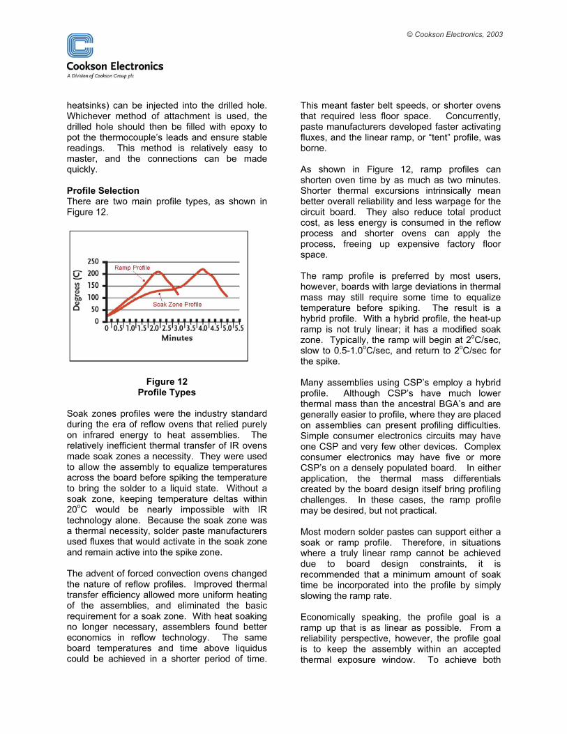
heatsinks) can be injected into the drilled hole. Whichever method of attachment is used, the drilled hole should then be filled with epoxy to pot the thermocouple’s leads and ensure stable readings. This method is relatively easy to master, and the connections can be made quickly. Profile Selection There are two main profile types, as shown in Figure 12.
Figure 12 Profile Types
Soak zones profiles were the industry standard during the era of reflow ovens that relied purely on infrared energy to heat assemblies. The relatively inefficient thermal transfer of IR ovens made soak zones a necessity. They were used to allow the assembly to equalize temperatures across the board before spiking the temperature to bring the solder to a liquid state. Without a soak zone, keeping temperature deltas within 20oC would be nearly impossible with IR technology alone. Because the soak zone was a thermal necessity, solder paste manufacturers used fluxes that would activate in the soak zone and remain active into the spike zone. The advent of forced convection ovens changed the nature of reflow profiles. Improved thermal transfer efficiency allowed more uniform heating of the assemblies, and eliminated the basic requirement for a soak zone. With heat soaking no longer necessary, assemblers found better economics in reflow technology. The same board temperatures and time above liquidus could be achieved in a shorter period of time.
This meant faster belt speeds, or shorter ovens that required less floor space. Concurrently, paste manufacturers developed faster activating fluxes, and the linear ramp, or “tent” profile, was borne. As shown in Figure 12, ramp profiles can shorten oven time by as much as two minutes. Shorter thermal excursions intrinsically mean better overall reliability and less warpage for the circuit board. They also reduce total product cost, as less energy is consumed in the reflow process and shorter ovens can apply the process, freeing up expensive factory floor space. The ramp profile is preferred by most users, however, boards with large deviations in thermal mass may still require some time to equalize temperature before spiking. The result is a hybrid profile. With a hybrid profile, the heat-up ramp is not truly linear; it has a modified soak zone. Typically, the ramp will begin at 2oC/sec, slow to 0.5-1.0oC/sec, and return to 2oC/sec for the spike. Many assemblies using CSP’s employ a hybrid profile. Although CSP’s have much lower thermal mass than the ancestral BGA’s and are generally easier to profile, where they are placed on assemblies can present profiling difficulties. Simple consumer electronics circuits may have one CSP and very few other devices. Complex consumer electronics may have five or more CSP’s on a densely populated board. In either application, the thermal mass differentials created by the board design itself bring profiling challenges. In these cases, the ramp profile may be desired, but not practical. Most modern solder pastes can support either a soak or ramp profile. Therefore, in situations where a truly linear ramp cannot be achieved due to board design constraints, it is recommended that a minimum amount of soak time be incorporated into the profile by simply slowing the ramp rate. Economically speaking, the profile goal is a ramp up that is as linear as possible. From a reliability perspective, however, the profile goal is to keep the assembly within an accepted thermal exposure window. To achieve both

© Cookson Electronics, 2003
these goals, good thermal transfer is the key to success. Conclusion Many assemblers are facing the challenges of implementing fine feature devices. In refining the solder paste printing process to accommodate fine feature electronic devices, process developers must not only seek to optimize the individual components of the process, but to optimize the process as a whole. Understanding the interdependence of the components is the key to success. In refining the profiling process, it is important to get obtain accurate readings, and to understand the tradeoffs and limitations imposed by both the circuit design and oven technology. High yield, robust processes currently exist for fine feature devices. They are the result of a multitude of studies on both the components and the interactions. Studies currently underway will continue to improve the industry’s understanding of soldering technology and further enhance assemblers’ capability to meet the next level of challenges in the future. References 1. Houston, P., “Defect Per Million Opportunity
Analysis of AlphaMetals 6106 for 0201 Assembly,” A study by Siemens Dematic Electronics Assembly Systems, December, 2001
2. Patent number 10/156,962 3. Wang, M, et al, “Investigation of Printing
Issue and Stencil Design for 0201 Package”, Proceedings of SMTA International, September, 2001
4. Wang, M., et al, “Board Design and Assembly Process Evaluation for 0201 Components on PCB’s, Proceedings of APEX 2002, January, 2002
5. Fleck, I., Chouta, P., “A New Dimension in Stencil Print Optimization”, Proceedings of SMTA International, September, 2002
6. Pham-van-Diep, G., “Real Time Visualization and Prediction of Solder Paste Flow in the Circuit Board Print Operation”, Proceedings of the SMTA Advanced Technology Symposium, June, 2002
7. Mendez, D., Clarke,R., “Statistical Model of Printed Wiring Board and Stencil Alignment
Issues”, Proceedings of Surface Mount Internantional Conference, April, 1997.
8. Johnson, A., Boyes, R., “Stencil Printing Basics: Equipment, Materials and Process Requirements”, Chip Scale Review, January/February 2002
9. Becker, A., Apell, M., “Classic PCB Profiling of the Reflow Solder Process”, Circuits Assembly, May 2001