printed, ßexible electrochromic displays using...
TRANSCRIPT
*Corresponding author.
Solar Energy Materials & Solar Cells 56 (1999) 395—418
Printed, flexible electrochromic displays usinginterdigitated electrodes
James P. Coleman!,*, Anne T. Lynch!,Puttanachetty Madhukar!, John H. Wagenknecht"! Monsanto, Growth Enterprises, 800 N. Lindbergh Blvd., St. Louis, MO 63167, USA
" Cedar Hill LLC, 7510 Horseplay Lane, Cedar Hill, MO 63016, USA
Abstract
We describe herein some of our initial studies in pursuit of a simple, economical method ofmass producing electrochromic displays. The approach we have taken is to print the display onpolymer film utilizing commercially available conductive inks in an interdigitated elect-rode structure with a conductive metal oxide powder, dispersed in a polymer binder, as theelectrode surface. A range of electrochromic materials suitable for use with an aqueous gelelectrolyte have been explored and examples presented. ( 1999 Elsevier Science B.V. Allrights reserved.
Keywords: Polymer film; Electrolyte; Electrochromic displays
1. Introduction
The conventional method of producing electrochromic displays has utilizeda “sandwich” configuration of electrodes, necessitating the use of at least one opticallytransparent electrode such as indium—tin oxide (ITO). Such electrodes, whilst workingvery well in laboratory cells, do not readily lend themselves to low cost massproduction and suffer a number of drawbacks. Disadvantages include cost, lowconductivity particularly on plastic substrates, difficulty of fabrication into sophisti-cated display designs and electrochemical instability leading to corrosion, particularlyin aqueous systems. [1].
0927-0248/99/$ — See front matter ( 1999 Elsevier Science B.V. All rights reserved.PII: S 0 9 2 7 - 0 2 4 8 ( 9 8 ) 0 0 1 4 4 - 5

Our target was a system wherein the production of raw materials and the construc-tion of displays utilizes only simple solution/dispersion processes and a low costprinting/coating approach to overcome the difficulties described above.
Instead of the conventional structure, we chose to develop an interdigitated elec-trode approach, wherein the electrodes are side-by-side and face up on a substrate.This type of design has been almost, but not completely [2,3] neglected for theconstruction of electrochromic displays and was, for instance, not discussed in arecent, excellent book on electrochromism [4]. We felt that this approach offered apotentially simpler manufacturing process and the opportunity to utilize a broaderrange of materials once the requirement for a transparent electrode had been eliminated.
We therefore pursued the design and fabrication of circuitry for a wide range ofinterdigitated displays, along with the development of the appropriate conductivecoatings, electrochromic materials and electrolytes, as will be described below.
2. Experimental
2.1. Circuits, printing and inks
The artwork for the circuits employed here was created using Autocad and AdobeIllustrator programs on a Macintosh Centrix 650 computer. This was then convertedinto 20]27 in screens for use on a Sakurai Maestro sheet-fed screen printing pressat Murfin, Columbus, Ohio. The substrate typically used was 0.007 inch clear poly-ester film, although we also used thinner film (0.005 in) and opaque, barium sulfate-pigmented polyester. Sealing was typically done with 0.005 in adhesive-coatedpolyester.
A variety of commercial silver and carbon inks from Acheson Colloids were used,including SS427 (silver) and SS24747 (graphite). For the insulating layer we usedAcheson ML25198, a UV-cured acrylic formulation. The ink for the conductive metaloxide electrode coating was prepared by dispersing 25% ATO-TiO
2(Mitsubishi W-1)
in a 22 wt% solution of Viton fluoroelastomer in 2-butoxyethyl acetate so as to givea 2.5 : 1 pigment-to-binder ratio. Inks formulated from conductive particles coatedwith electrochromic materials were similarly prepared.
For laboratory test purposes, samples of exploratory inks were applied witha drawbar and dried in an oven at 130°C for 10 min.
2.2. Electrochromic materials
The preparation of a typical electrochromic-coated conductive pigment will beexemplified using Prussian blue as an example. Ferrous sulfate (0.6 g) was dissolved indeionised water (150 m). To this solution was added conductive pigment DupontECP-1703-S (15.0 g, 65 wt% ATO on silica shells), with stirring. To the well-stirredslurry was added, dropwise, a solution of potassium ferricyanide (0.45 g) in water(23 m). The resulting deep blue slurry was filtered and the wet cake was pressed as dryas possible before drying under vacuum at 110°C to give a deep blue powder.
396 J.P. Coleman et al. /Solar Energy Materials & Solar Cells 56 (1999) 395—418

2.3. Electrolytes
All chemicals used were from Aldrich unless otherwise stated. A typical electrolytefor a bismuth display contained 33 wt% calcium chloride, 4.7% hydroxyethyl cellu-lose (Union Carbide Cellosize W8163L), 2.35% bismuth trichloride, 0.235% cupricchloride, 0.5% concentrated hydrochloric acid and 0.2% Triton X-100 surfactant(Fisher) in water. The amount of copper was varied over a range from 0% to 50% ofthe bismuth concentration in different formulations. For viologen displays we usedtwo different electrolytes as follows:
(1) 20% lithium bromide, 10% hydroxyethyl cellulose, 0.5% heptyl viologen, and0.1% Triton X-100 (Fisher) in water or (2) 20% sodium nitrate, 10% hydroxyethylcellulose, and 0.75% heptyl viologen in water. For Prussian blue displays, in thework reported here, we used either a 25% potassium chloride solution or a 25%potassium formate solution, thickened with 2% agar. The colored pigments whichwere added to Prussian blue inks were HI-VIZTM fluorescent pigments from LawterInternational.
2.4. Analytical measurements
Voltammetry and coulometry were carried out with a PAR Model 273A usingM270 software. Reflectance measurements were performed using a Nikon MicrophotFXL microscope with a Melles—Griot photosensor mounted on it. A darkfieldattachment was used to exclude specular reflectance. The output of the photosensoramplifier was displayed on a Hewlett-Packard 54501A digitizing oscilloscope and thesystem was calibrated using a Kodak black/white standard. Reflectance spectra wereobtained with a Hunter Lab Ultrascan spectrometer. Scanning electron microscopywas carried out using a JEOL 840 microscope. Transmission electron microscopy wascarried out with a JEOL JEM 2000FX microscope and high-resolution TEM witha JEM 4000EX.
3. Results
3.1. Overview
After screening several different approaches, the following methodology was ad-opted for display construction. The appropriate circuit was designed and screen-printed on polymer film with silver ink. A conforming layer of carbon ink was thenprinted on top of the silver to provide corrosion protection. Connecting leads werethen covered with a printed insulator, leaving contact tabs exposed at the ends. Theactual electrode surface was then printed with a dispersion of a light-colored conduc-tive metal oxide powder in a polymer binder. The electrochromic material was eithercontained in this layer, printed on the surface or dissolved in the aqueous gelelectrolyte which was put down last, prior to sealing with a transparent polymer film.If a thicker electrolyte layer was desired, we placed a “frame” of adhesive mylar
J.P. Coleman et al. /Solar Energy Materials & Solar Cells 56 (1999) 395—418 397

Fig. 1. Display cross section.
around the edge of the display, before the electrolyte was added, to help contain theelectrolyte and prevent it from being squeezed out.
Fig. 1 shows a schematic cross section of the type of cell used in this approach.Current flow in this type of cell moves vertically through the conductive metal oxidedispersion to the interface of the electrochromic material and the electrolyte where theelectrochromic color change takes place. Ionic current flow through the electrolytecompletes the circuit. It may be seen that, as shown in Fig. 1, there is an apparentshort circuit through the conductive metal oxide layer. The impact of this short circuitis kept to a minimum in practice by keeping the interelectrode spacing significantlylarger than the thickness of the metal oxide coating. The thickness of the metal oxidecoating between the electrodes may be further decreased by printing a layer ofinsulator between the electrodes, as shown. In addition, the conductivity of theelectrolyte plays a key role in maximizing current flow through the desired path andmust therefore be as high as possible. We can, of course, print a gap in the metal oxidecoating between the electrodes. This is acceptable with certain display designs, e.g.7]5 arrays, but is less aesthetically pleasing with other designs where the imageoutline is intended to be invisible until switched on.
A typical display would be fabricated using polyester film (0.005—0.007 in.) assubstrate and sealing layer. Conductive and active layers would be about 0.002 in.thick (total) and the electrolyte about 0.010 in. for a total device thickness of around0.025 inches. Significantly thinner devices are possible, depending on image size andswitching speeds desired, as are much thicker displays, e.g. laminated between sheetsof glass.
3.2. Circuit design
The process of designing an interdigitated display circuit begins with the desiredimages, to which we add connecting leads and counter electrodes, and is completed by
398 J.P. Coleman et al. /Solar Energy Materials & Solar Cells 56 (1999) 395—418
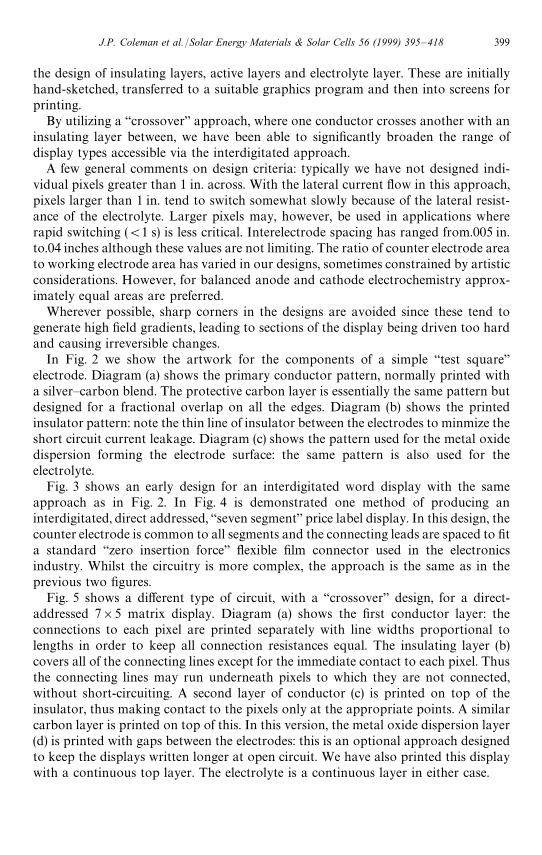
the design of insulating layers, active layers and electrolyte layer. These are initiallyhand-sketched, transferred to a suitable graphics program and then into screens forprinting.
By utilizing a “crossover” approach, where one conductor crosses another with aninsulating layer between, we have been able to significantly broaden the range ofdisplay types accessible via the interdigitated approach.
A few general comments on design criteria: typically we have not designed indi-vidual pixels greater than 1 in. across. With the lateral current flow in this approach,pixels larger than 1 in. tend to switch somewhat slowly because of the lateral resist-ance of the electrolyte. Larger pixels may, however, be used in applications whererapid switching ((1 s) is less critical. Interelectrode spacing has ranged from.005 in.to.04 inches although these values are not limiting. The ratio of counter electrode areato working electrode area has varied in our designs, sometimes constrained by artisticconsiderations. However, for balanced anode and cathode electrochemistry approx-imately equal areas are preferred.
Wherever possible, sharp corners in the designs are avoided since these tend togenerate high field gradients, leading to sections of the display being driven too hardand causing irreversible changes.
In Fig. 2 we show the artwork for the components of a simple “test square”electrode. Diagram (a) shows the primary conductor pattern, normally printed witha silver—carbon blend. The protective carbon layer is essentially the same pattern butdesigned for a fractional overlap on all the edges. Diagram (b) shows the printedinsulator pattern: note the thin line of insulator between the electrodes to minmize theshort circuit current leakage. Diagram (c) shows the pattern used for the metal oxidedispersion forming the electrode surface: the same pattern is also used for theelectrolyte.
Fig. 3 shows an early design for an interdigitated word display with the sameapproach as in Fig. 2. In Fig. 4 is demonstrated one method of producing aninterdigitated, direct addressed, “seven segment” price label display. In this design, thecounter electrode is common to all segments and the connecting leads are spaced to fita standard “zero insertion force” flexible film connector used in the electronicsindustry. Whilst the circuitry is more complex, the approach is the same as in theprevious two figures.
Fig. 5 shows a different type of circuit, with a “crossover” design, for a direct-addressed 7]5 matrix display. Diagram (a) shows the first conductor layer: theconnections to each pixel are printed separately with line widths proportional tolengths in order to keep all connection resistances equal. The insulating layer (b)covers all of the connecting lines except for the immediate contact to each pixel. Thusthe connecting lines may run underneath pixels to which they are not connected,without short-circuiting. A second layer of conductor (c) is printed on top of theinsulator, thus making contact to the pixels only at the appropriate points. A similarcarbon layer is printed on top of this. In this version, the metal oxide dispersion layer(d) is printed with gaps between the electrodes: this is an optional approach designedto keep the displays written longer at open circuit. We have also printed this displaywith a continuous top layer. The electrolyte is a continuous layer in either case.
J.P. Coleman et al. /Solar Energy Materials & Solar Cells 56 (1999) 395—418 399

Fig. 2. Printed test square components.
These examples are representative of the many types of displays we have designed,ranging from words and numerical displays to clocks, moving beer glasses andbasketballs. We are continuing to probe the limits of sophistication of the inter-digitated approach for making displays.
3.3. Conductors
For the patterned conductors used in this approach, we have studied a variety ofmaterials including silver and silver—carbon inks, carbon/graphite ink, electroless
400 J.P. Coleman et al. /Solar Energy Materials & Solar Cells 56 (1999) 395—418

Fig. 3. Components of a printed word display.
copper on polymer films, photo-patterned aluminum on polymer films, electrolessnickel, polyaniline, conductive metal oxides, and sputtered gold on polymer films. Wechose to use commercially available silver and silver—carbon inks which offer a goodcombination of conductivity and ease of printing into detailed circuitry with fineresolution. The silver layer is then typically overprinted with a layer of corrosion-resistant carbon ink in the same pattern, slightly overlapping the edges of the silver.
3.4. Insulators
As mentioned above, it is necessary to insulate any conductor surface which we donot want to appear in the electrochromic image.
J.P. Coleman et al. /Solar Energy Materials & Solar Cells 56 (1999) 395—418 401
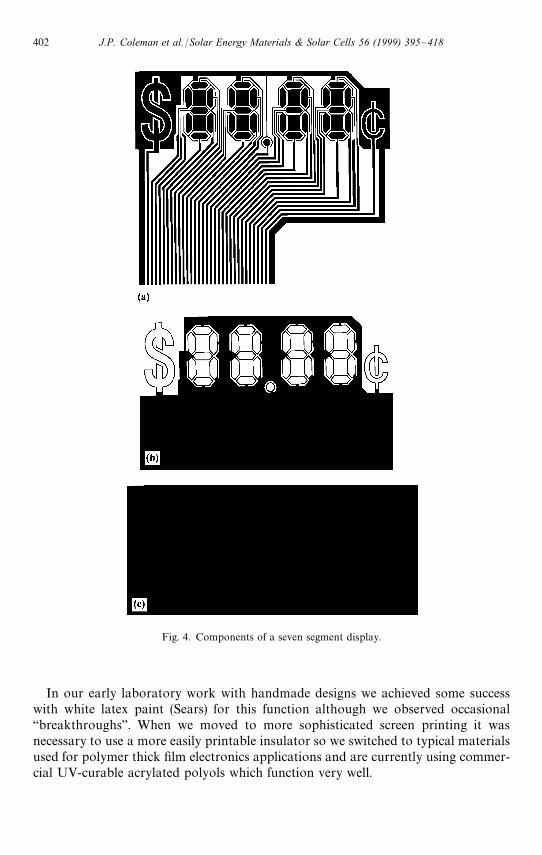
Fig. 4. Components of a seven segment display.
In our early laboratory work with handmade designs we achieved some successwith white latex paint (Sears) for this function although we observed occasional“breakthroughs”. When we moved to more sophisticated screen printing it wasnecessary to use a more easily printable insulator so we switched to typical materialsused for polymer thick film electronics applications and are currently using commer-cial UV-curable acrylated polyols which function very well.
402 J.P. Coleman et al. /Solar Energy Materials & Solar Cells 56 (1999) 395—418
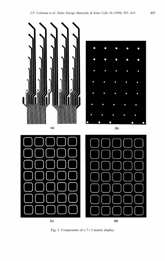
Fig. 5. Components of a 7]5 matrix display.
J.P. Coleman et al. /Solar Energy Materials & Solar Cells 56 (1999) 395—418 403

3.5. Metal oxide electrode surface layer
The requirements for the actual electrode surface layer are that it is conductive,light in color, in order to observe electrochromic transformations, and stable bothchemically and electrochemically under conditions of operation, in our case in anaqueous environment. In addition, the material needs to be easily configurable,preferably printable. To meet these criteria we investigated the use of conductivemetal oxide powders dispersed in polymer binder solutions to form inks. We firstlooked at the use of indium—tin oxide (ITO) powder which, at the time, we groundfrom chunks of ITO (Puretech). This somewhat coarse powder was dispersed ina solution of styrene—butadiene copolymer in toluene to give an ink. When this wascoated onto copper plated onto mylar film, in the form of simple side-by-sideelectrodes, we were able to carry out electrochemistry at the metal oxide surface, suchas the electrodeposition and electrochromic cycling of polyaniline in aqueous acidsolutions. Encouraged by this successful demonstration, we looked for conductivemetal oxide powders which could be similarly used but with improved aesthetics andeconomics. We found that a number of light-colored conductive pigments wereavailable commercially, typically based on antimony-doped tin oxide deposited ontoinert light-scattering pigments such as TiO
2. Companies producing such pigments
include Dupont, Mitsubishi and Mitsui.The first of these commercial products we studied was Mitsubishi W-1, 25%
antimony—tin oxide on TiO2. This material is an off-white, fine powder with an
electrical resistivity of about 5 )cm (12,000 psig). We were able to formulate thispowder, with a variety of polymer binders, into inks which provided an almost whiteelectrode surface on which we could carry out a variety of electrochemical reactions,as will be discussed below. Sheet resistance of these coatings is fairly high-10—20 K)/square - but quite sufficient given the short distance of the current paththrough the coating (ca. 0.001 in). The stability of these coatings towards aqueouselectrolytes is quite good: since the conductor is a doped tin oxide it is, of course,susceptible to overreduction and loss of conductivity on being driven to excessivepotentials in the cathodic direction [1]. However, since the thickness of these printedcoatings is greater than the typical transparent tin oxide or ITO electrode, ca 25 lmvs. 1 lm, these electrodes are considerably more resilient, particularly since theprimary conductor is the silver layer underneath.
3.6. Electrochromic materials
A wide variety of electrochromic materials have been studied and a number ofdifferent approaches taken. Electrochromic materials which are soluble in the aque-ous electrolyte include methyl viologen, heptyl viologen and metal ions which may beelectroplated, such as bismuth(III). Examples of these and other types will be dis-cussed below. Insoluble electrochromic materials such as Prussian Blue, poly(xylylviologen) — poly(styrenesulfonate) or polyaniline may be either coated onto the surfaceof the metal oxide composite electrode or coated onto the conductive pigmentparticles prior to formulating the ink. Similarly, it is possible to make “hybrid” devices
404 J.P. Coleman et al. /Solar Energy Materials & Solar Cells 56 (1999) 395—418

by sputtering or evaporating electrochromic materials such as tungsten oxide onto thesurface of the printed electrode. Finally, preformed, insoluble electrochromic mater-ials, such as commercially available perylene imide pigments, may simply be mixedwith the conductive pigment prior to ink formation, although this approach issomewhat less efficient than a more intimate coating.
3.7. Ink formulation
Following our initial probe studies on formulating conductive metal oxide pig-ments into inks, we decided to work with a commercial ink company, AchesonColloids, a major manufacturer of conductive and related inks for the electronicsindustry, to develop further formulations. A number of binder—solvent systems werescreened and, for this work, we used a Viton fluoroelastomer dissolved in 2-butoxyethyl acetate as the vehicle. Pigment-to-binder ratio for the conductive metaloxide, or electrochromic-coated metal oxide, was typically about 2.5 : 1. Higherbinder levels gave increased electrical resistance whilst significantly lower binderlevels gave a less stable, chalky coating. We also demonstrated that it is possible toincorporate commercially available fluorescent colored pigments into these inks inorder to produce brighter colored displays.
3.8. Electrolytes
For this display configuration, electrolyte requirements are somewhat differentthan for a conventional “sandwich” cell. As may be seen from Fig. 1, the possible ioniccurrent path may be up to half the combined width of both electrodes, or even longerdepending on the electrode configuration. For this reason it is desirable to keep theelectrolyte resistance as low as possible in order to minimize field gradients and this, inturn, suggests aqueous salt solutions as the electrolytes of choice. For the workdescribed here, and depending on the electrochromic material used, the electrolyte hastypically contained a combination of a polymeric thickening agent and a hygroscopicsalt. Polymers used include hydroxyethyl cellulose, polyacrylic acid and poly-AMPS(poly [acrylamidoMmethylpropane sulfonic acidN]). Salts have included lithium chlor-ide, potassium chloride, potassium formate, lithium bromide and calcium chloride.
3.9. Sealing films
Since the top layer of electrolyte is not, in this work, a solid, and we wish to retardthe evaporation of water as much as possible, it is necessary to seal the display with aninert transparent layer. Glass, of course, is a possibility but this would detract from theflexibility and ease of production of the display. Commercial polyester film (MylarTM)offers a good combination of transparency, water barrier properties, cost and avail-ability. Whilst other materials, e.g. Aclar, might offer better barrier properties they aresignificantly more expensive and difficult to process. Less expensive films such as PVChave less acceptable barrier properties.
J.P. Coleman et al. /Solar Energy Materials & Solar Cells 56 (1999) 395—418 405

3.10. Display drivers
Since our aim was to produce low cost electrochromic displays, it was necessary toconsider the whole package including driver electronics. In the laboratory we have theluxury of using a variety of sophisticated driver methods e.g. potentiostatic, constantcurrent, fixed charge, etc. However, a low cost display package probably has to bedriven by fairly simple electronics. Our displays have been targeted for operation at1.5 v or less, thus being operable by a single flashlight battery. We have thereforeconstructed a series of drivers of increasing sophistication to activate our displays.The simplest is a “manual” driver with a 1.5 v battery and a reversing switch. This wasautomated electronically to give a $1.5 v output with cycle time adjustable witha capacitor. This driver cycles continuously at the desired frequency.
For multi-element “motion” displays we constructed, for test purposes, a 12-output,variable voltage, variable time driver. This was then simplified into a “breadboard”design for a four output $1.5 v driver where cycle time was controlled with anexternal capacitor and the boards could be “daisy-chained” in multiple units. Thisbreadboard was then used as the basis for an application-specific integrated circuit(ASIC) with the same functionality. For more complex displays such as 7-segment and7]5 matrix displays, we have had built prototype electronics (Polyvision, Wallin-gford, Connecticut) and plan to move these to the ASIC stages as the programprogresses.
3.11. Display examples
Our approach will be illustrated here by reference to some specific examples,fabricated primarily with ATO-TiO
2(Mitsubishi) as the electrode coating. Fig. 6
shows a “test square” coated with one of the first materials we studied — polyaniline-tosylate. In this example we coated the polyaniline onto the conductive particles as itwas synthesized and then formulated the composite particles into an ink. The displayshown uses poly(AMPS) as the electrolyte and utilizes all three oxidation states ofpolyaniline during redox cycling, as may be seen from the electrode colors in the twoopposite states with working electrode anodic (a) and cathodic (b). Fig. 7 showsintegrated reflectivity versus time for this device, switched at $ 1.5 v. Overall this isnot a very bright display; darkening to almost full darkness takes place in about 1 sbut full recovery takes a little longer. Faster cycling is possible at higher voltages. At$ 1.5 v at 0.5 Hz, coulometry showed the consumption of 6.1 mC/cm2. Whilst thiswas a useful early functional example, its visual attractiveness left something to bedesired and it was not pursued as a commercial candidate. Fig. 8 shows a displayutilizing heptyl viologen in a thickened lithium bromide electrolyte. This was an earlycircuit design for letters where we had not optimized the relative configurations ofworking and counter electrodes and thus the letters were not “written” all the way tothe center. This problem has been addressed in subsequent designs. For this type ofdisplay we were interested in driving it in a continuous $ reversing contrast mode.Therefore, no additional counter electrode reaction was necessary after the firsthalf-cycle on initiating the display and a lithium bromide electrolyte was satisfactory.
406 J.P. Coleman et al. /Solar Energy Materials & Solar Cells 56 (1999) 395—418

Fig. 6. Polyaniline-coated test square.
Fig. 9 shows reflectance versus time for a viologen display — significantly brighter thanthe polyaniline display, although using less current (4.0 mC/cm2). Whilst viologensgive an attractive display in the short term, we have found, as have other workers [5],that on prolonged cycling, irreversible colored deposits are formed, seriously detract-ing from the aesthetics of the display. We have not yet found a viologen which is free ofthis problem in our system.
Fig. 10 shows an example of bismuth plating as the electrochromic reaction. Thebismuth system has been extensively studied by Warszawski and co-workers [6]and by Howard and Ziegler [7]. In a transparent electrode cell the electrolyte forbismuth deposition typically contains lithium bromide and copper (II) in addition tobismuth (III). The resulting red-brown color of this solution is masked by the additionof a pigment such as TiO
2against which the plating of black bismuth metal is
observed through the transparent electrode. With our configuration, we need to seethrough the electrolyte to the electrode behind it and thus we cannot use an opaque
J.P. Coleman et al. /Solar Energy Materials & Solar Cells 56 (1999) 395—418 407

Fig. 7. Reflectance vs. time for polyaniline—polyamps ($1.5V).
Fig. 8. Heptyl viologen-based word display.
408 J.P. Coleman et al. /Solar Energy Materials & Solar Cells 56 (1999) 395—418
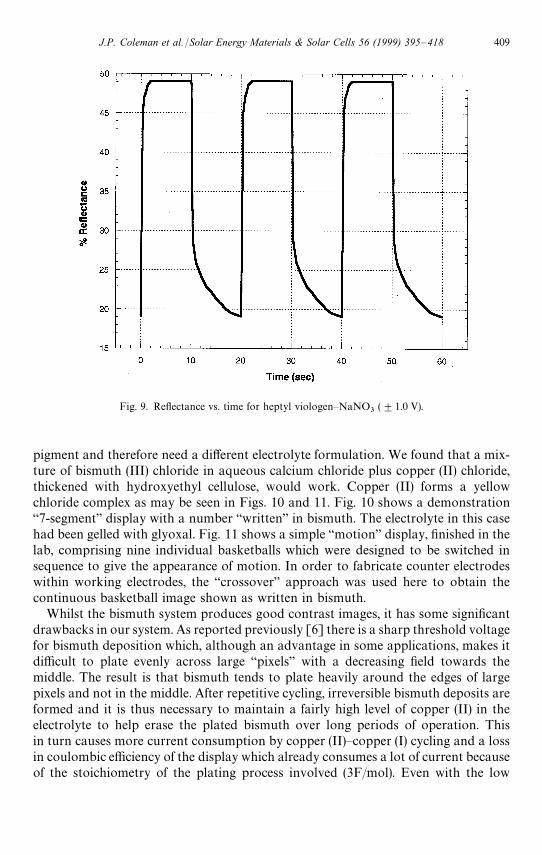
Fig. 9. Reflectance vs. time for heptyl viologen—NaNO3
($1.0 V).
pigment and therefore need a different electrolyte formulation. We found that a mix-ture of bismuth (III) chloride in aqueous calcium chloride plus copper (II) chloride,thickened with hydroxyethyl cellulose, would work. Copper (II) forms a yellowchloride complex as may be seen in Figs. 10 and 11. Fig. 10 shows a demonstration“7-segment” display with a number “written” in bismuth. The electrolyte in this casehad been gelled with glyoxal. Fig. 11 shows a simple “motion” display, finished in thelab, comprising nine individual basketballs which were designed to be switched insequence to give the appearance of motion. In order to fabricate counter electrodeswithin working electrodes, the “crossover” approach was used here to obtain thecontinuous basketball image shown as written in bismuth.
Whilst the bismuth system produces good contrast images, it has some significantdrawbacks in our system. As reported previously [6] there is a sharp threshold voltagefor bismuth deposition which, although an advantage in some applications, makes itdifficult to plate evenly across large “pixels” with a decreasing field towards themiddle. The result is that bismuth tends to plate heavily around the edges of largepixels and not in the middle. After repetitive cycling, irreversible bismuth deposits areformed and it is thus necessary to maintain a fairly high level of copper (II) in theelectrolyte to help erase the plated bismuth over long periods of operation. Thisin turn causes more current consumption by copper (II)—copper (I) cycling and a lossin coulombic efficiency of the display which already consumes a lot of current becauseof the stoichiometry of the plating process involved (3F/mol). Even with the low
J.P. Coleman et al. /Solar Energy Materials & Solar Cells 56 (1999) 395—418 409
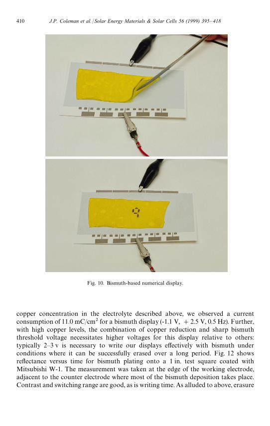
Fig. 10. Bismuth-based numerical display.
copper concentration in the electrolyte described above, we observed a currentconsumption of 11.0 mC/cm2 for a bismuth display (-1.1 V, #2.5 V, 0.5 Hz). Further,with high copper levels, the combination of copper reduction and sharp bismuththreshold voltage necessitates higher voltages for this display relative to others:typically 2—3 v is necessary to write our displays effectively with bismuth underconditions where it can be successfully erased over a long period. Fig. 12 showsreflectance versus time for bismuth plating onto a 1 in. test square coated withMitsubishi W-1. The measurement was taken at the edge of the working electrode,adjacent to the counter electrode where most of the bismuth deposition takes place.Contrast and switching range are good, as is writing time. As alluded to above, erasure
410 J.P. Coleman et al. /Solar Energy Materials & Solar Cells 56 (1999) 395—418

Fig. 11. Bismuth-based basketball display.
J.P. Coleman et al. /Solar Energy Materials & Solar Cells 56 (1999) 395—418 411
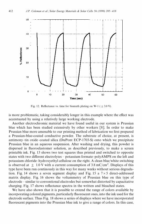
Fig. 12. Reflectance vs. time for bismuth plating on W-1 ($3.0 V).
is more problematic, taking considerably longer in this example where the effect wasaccentuated by using a relatively large working electrode.
Another electrochromic material we have found useful in our system is Prussianblue which has been studied extensively by other workers [8]. In order to makePrussian blue more amenable to our printing method of fabrication we first prepareda Prussian-blue-coated conductive powder. The substrate of choice, at present, isantimony—tin oxide—coated silica (DuPont ECP-1703-S) onto which we precipitatePrussian blue in an aqueous suspension. After washing and drying, this powder isdispersed in fluoroelastomer solution, as described previously, to make a screenprintable ink. Fig. 13 shows two test squares thus printed and switched to oppositestates with two different electrolytes — potassium formate—polyAMPS on the left andpotassium chloride—hydroxyethyl cellulose on the right. A clean blue/white switchingis observed at $ 1.0 V with a current consumption of 3.8 mC/cm2. Displays of thistype have been run continously in this way for many weeks without serious degrada-tion. Fig. 14 shows a seven segment display and Fig. 15 a 7]5 direct-addressedmatrix display. Fig. 16 shows the voltammetry of Prussian blue on this type ofelectrode — similar to conventional electrodes but somewhat distorted by capacitativecharging. Fig. 17 shows reflectance spectra in the written and bleached states.
We have also shown that it is possible to extend the range of colors available byincorporating colored pigments, particularly fluorescent ones, into the ink used for theelectrode surface. Thus Fig. 18 shows a series of displays where we have incorporatedfluorescent pigments into the Prussian blue ink to give a range of colors. In this case,
412 J.P. Coleman et al. /Solar Energy Materials & Solar Cells 56 (1999) 395—418

Fig. 13. Prussian blue test squares.
Fig. 14. Prussian blue seven segment display.
J.P. Coleman et al. /Solar Energy Materials & Solar Cells 56 (1999) 395—418 413
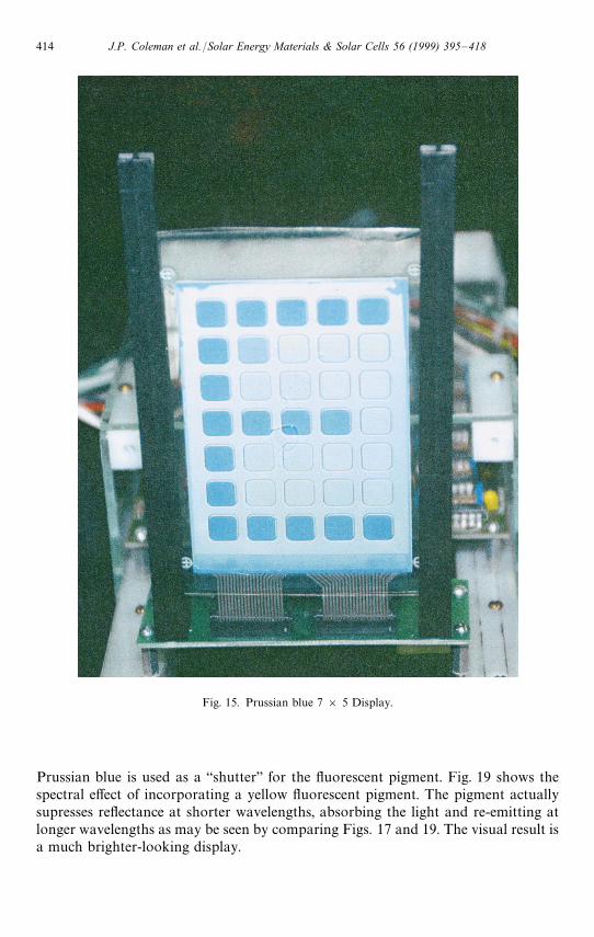
Fig. 15. Prussian blue 7 ] 5 Display.
Prussian blue is used as a “shutter” for the fluorescent pigment. Fig. 19 shows thespectral effect of incorporating a yellow fluorescent pigment. The pigment actuallysupresses reflectance at shorter wavelengths, absorbing the light and re-emitting atlonger wavelengths as may be seen by comparing Figs. 17 and 19. The visual result isa much brighter-looking display.
414 J.P. Coleman et al. /Solar Energy Materials & Solar Cells 56 (1999) 395—418

Fig. 16. Cyclic voltammetry of Prussian blue—10% KCl (2.7% PB on ATO—Silica Shells.
Fig. 17. Diffuse reflectance spectrum of Prussian blue plus potassium formate/agar ($1.5 V).
J.P. Coleman et al. /Solar Energy Materials & Solar Cells 56 (1999) 395—418 415

Fig. 18. Displays with Prussian blue plus fluorescent pigments.
416 J.P. Coleman et al. /Solar Energy Materials & Solar Cells 56 (1999) 395—418
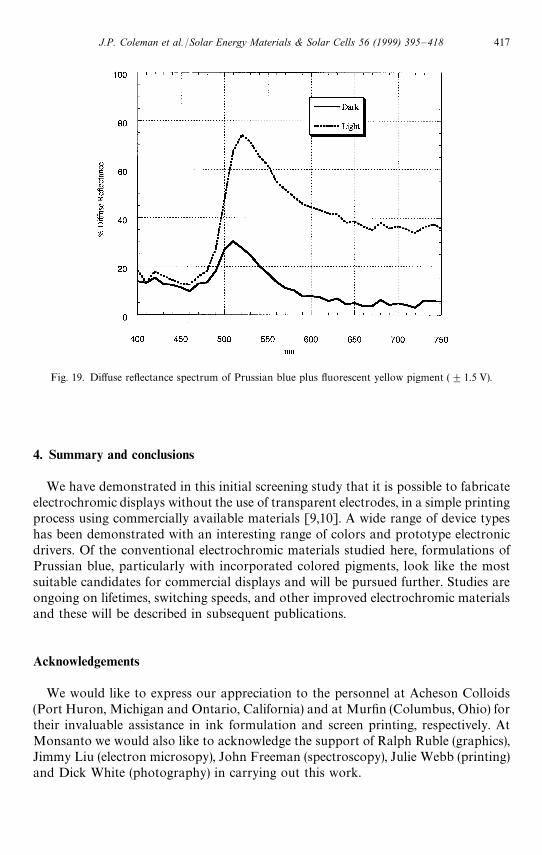
Fig. 19. Diffuse reflectance spectrum of Prussian blue plus fluorescent yellow pigment ($1.5 V).
4. Summary and conclusions
We have demonstrated in this initial screening study that it is possible to fabricateelectrochromic displays without the use of transparent electrodes, in a simple printingprocess using commercially available materials [9,10]. A wide range of device typeshas been demonstrated with an interesting range of colors and prototype electronicdrivers. Of the conventional electrochromic materials studied here, formulations ofPrussian blue, particularly with incorporated colored pigments, look like the mostsuitable candidates for commercial displays and will be pursued further. Studies areongoing on lifetimes, switching speeds, and other improved electrochromic materialsand these will be described in subsequent publications.
Acknowledgements
We would like to express our appreciation to the personnel at Acheson Colloids(Port Huron, Michigan and Ontario, California) and at Murfin (Columbus, Ohio) fortheir invaluable assistance in ink formulation and screen printing, respectively. AtMonsanto we would also like to acknowledge the support of Ralph Ruble (graphics),Jimmy Liu (electron microsopy), John Freeman (spectroscopy), Julie Webb (printing)and Dick White (photography) in carrying out this work.
J.P. Coleman et al. /Solar Energy Materials & Solar Cells 56 (1999) 395—418 417

References
[1] H.A. Laitinen, C.A. Vincent, T.M. Bednarski, J. Electrochem. Soc. 115 (1968) 1024.[2] M. Brandon, B. Piggin, IBM Tech. Discl. Bull. 21 (1978) 2047.[3] N. Leventis, M. Wrighton, U.S. 5,189,549 (1993).[4] P.M.S. Monk, R.J. Mortimer, D.R. Rosseinsky, Electrochromism: Fundamentals and Applications,
VCH, 1995.[5] N.J. Goddard, A.C. Jackson, M.G. Thomas, J. Electroanal. Chem. 159 (1983) 325.[6] B. Warszawski, ECS Ext. Abs. 92-2 (1992, T) 785.[7] J.P. Ziegler, B.M. Howard, Solar Energy Mater. Solar Cells 39 (1995) 317.[8] K. Itaya, I. Uchida, V.D. Neff, Acc. Chem. Res. 19 (1986) 162.[9] J.P. Coleman, US 5,413,739 (1995).
[10] J.P. Coleman, US 5,500,759 (1996).
418 J.P. Coleman et al. /Solar Energy Materials & Solar Cells 56 (1999) 395—418