printed circuit boards (pcb) · diameter. allows judgement of ... (usually four small metal bridges...
TRANSCRIPT

11/12/2002 EE6471 (KR) 259
PCBs/Overview
– Printed Circuit Boards (PCB)• Introduction
• Conductors. Supply Planes. Dielectric.
• Vias
• PCB Manufacturing Process
• Electronic Assembly Manufacturing Process

11/12/2002 EE6471 (KR) 260
PCBs/Overview– For electronic
assemblies PCBs are substrates providing mechanical support as well as electrical interconnect
– PCB: Ridig or flexible substrate with single or multiple layers of conductors separated by insulating layers
Note: PCBs are sometimes also referred to as PWBs (Printed Wiring Boards)
11/12/2002 EE6471 (KR) 261
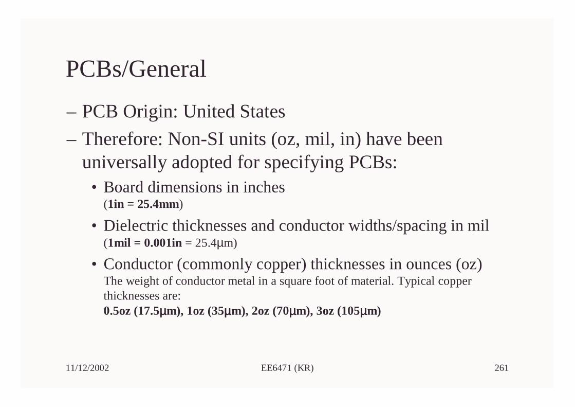
PCBs/General
– PCB Origin: United States
– Therefore: Non-SI units (oz, mil, in) have been universally adopted for specifying PCBs:
• Board dimensions in inches(1in = 25.4mm)
• Dielectric thicknesses and conductor widths/spacing in mil(1mil = 0.001in = 25.4µm)
• Conductor (commonly copper) thicknesses in ounces (oz)The weight of conductor metal in a square foot of material. Typical copper thicknesses are:0.5oz (17.5µµµµm), 1oz (35µµµµm), 2oz (70µµµµm), 3oz (105µµµµm)

11/12/2002 EE6471 (KR) 262
PCBs/General
– PCB General Specifications:• Finished thicknesses
– Standard: 31mil, 39mil and 62mil (0.8mm, 1.0mm and 1.6mm)
– Non-standard:
» Readily available for high-volume orders
» Board thicknesses: 10mil-125mil(many PCB manufacturers stop at 20mil - depending on plating finish)
• Maximum dimensions typically 16in x 20in
• Irregular shapes/slots etc readily available (routing)

11/12/2002 EE6471 (KR) 263
PCBs/Stackup
– Typical PCB Stackup:• Alternating layers of core and prepreg• Core: Thin piece of dielectric with copper foil bonded to both sides. Core
dielectric is cured fiberglass-epoxy resin• Prepreg: Uncured fiberglass-epoxy resin. Prepreg will cure (i.e. harden)
when heated and pressed• Outermost layers are prepreg with copper foil bonded to the outside (surface
foils)• To avoid crosstalk: Wires on adjacent signal layers are routed mostly
orthogonally• Stackup is symmetric about the center of the board in the vertical axis to
avoid mechanical stress in the board under thermal cycling
Shown: Cross-section of a typical 8-layer PCB Stackup
Prepreg
Core
Prepreg
Core
Prepreg
Prepreg
Core

11/12/2002 EE6471 (KR) 264
PCBs/Conductors
– Conductor:• Material: Typically Cu
• Number of layers:– Single or multilayer (up to 20 layers, and more)
– Dedicated supply layers (also called “ground layers”, “ground planes”)
– Most popular: 4-8 signal layers plus 4-8 ground layers
• Material dimensions:– Thicknesses: 0.5oz-3oz typically. 0.5oz/1oz standard for inner layers.
– Trend: towards 0.25oz (particularly for laminated IC packages)
– Width and spacing: ≥ 5mil

11/12/2002 EE6471 (KR) 265
PCBs/Stackup
– Power Planes:• Power planes are typically built on thinnest core available from a fabrication
vendor to maximize the capacitance between the planes
• Power planes often use thicker copper layers than signal layers to reduce resistance
– Why power planes?• Provide stable reference voltages for signals
• Distribute power to all devices
• Control cross-talk between signals
Shown: Cross-section of a typical 8-layer PCB Stackup
Prepreg
Core
Prepreg
Core
Prepreg
Prepreg
Core

11/12/2002 EE6471 (KR) 266
PCBs/Conductors
– PCB sheet resistances• Cu resistivity ρ=1.7*10-8Ω/m
• Remember: Sheet resistance…W
LRs
Wh
L
A
LR =
⋅⋅=⋅= ρρ
Wh L
PCB Sheet Resistances at T=300K(TC Copper: +3930ppm)
Conductor Rs in µΩµΩµΩµΩ
PCB Copper Track (0.5oz Cu) 971
PCB Copper Track (1oz Cu) 486
PCB Copper Track (2oz Cu) 243
PCB Copper Track (3oz Cu) 162
11/12/2002 EE6471 (KR) 267
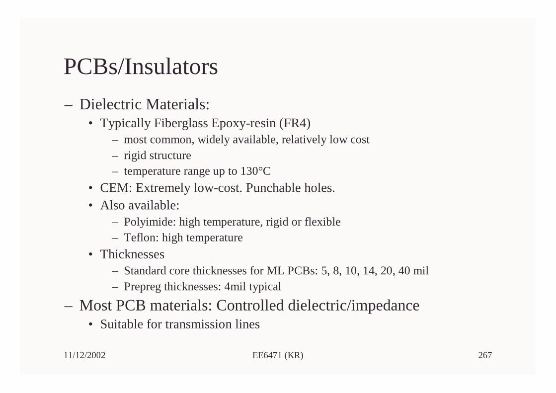
PCBs/Insulators
– Dielectric Materials:• Typically Fiberglass Epoxy-resin (FR4)
– most common, widely available, relatively low cost– rigid structure– temperature range up to 130°C
• CEM: Extremely low-cost. Punchable holes.• Also available:
– Polyimide: high temperature, rigid or flexible– Teflon: high temperature
• Thicknesses– Standard core thicknesses for ML PCBs: 5, 8, 10, 14, 20, 40 mil– Prepreg thicknesses: 4mil typical
– Most PCB materials: Controlled dielectric/impedance• Suitable for transmission lines

11/12/2002 EE6471 (KR) 268
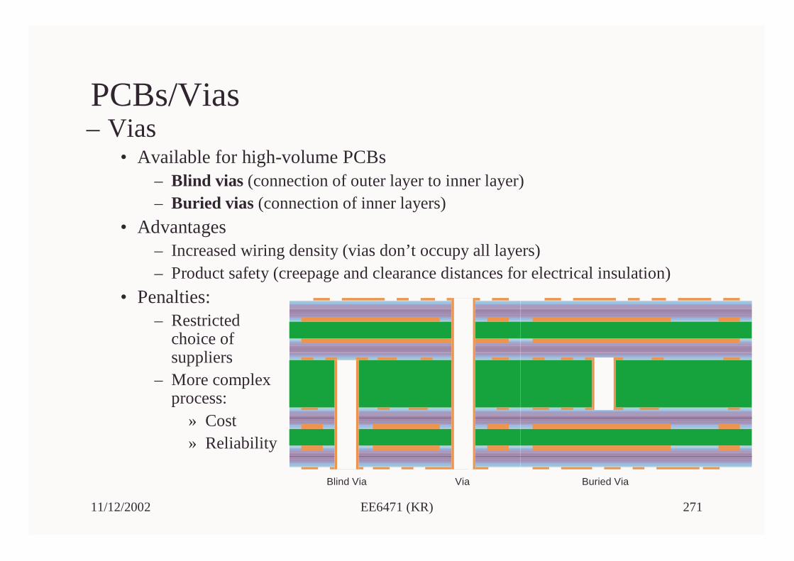
PCBs/Vias– Vias
• Interconnect layers through vias (plated holes)
• Via dimensions:– Standard minimum finished hole sizes: ≥ 8mil
– Aspect ratio restrictions
Aspect ratio of a via: Ratio of board thickness to via diameter. Allows judgement of manufacturability. The larger the aspect ratio, the more difficult it is to achieve reliable plating. Premium charge for aspect ratios > 8.

11/12/2002 EE6471 (KR) 269
PCBs/Vias– Vias
• Vias require pads on each layer to which they connect. Because the holes are not guaranteed to be perfectly aligned with the copper traces there will need to be an annulus of copper around the plated hole. This is to ensure that the copper won’t be broken by the drilling operation
• Pads on inner vias are larger than outer pads to allow for greater dimensional tolerances
• Where a via passes through a plane (i.e. not connect to the plane) a clearance hole is required
• Where a via is supposed to connect to aplane, a thermal relief structure is required(usually four small metal bridges betweenvia and plane). Thermal relief is requiredto facilitate soldering operations.

11/12/2002 EE6471 (KR) 270
PCBs/Vias
– Vias• Vias are much larger than signal wires
• Vias occupy all layers (with the exception of blind and buried vias)
• Consequence:Vias reduce wiring densityand are therefore expensive!
11/12/2002 EE6471 (KR) 271
PCBs/Vias– Vias
• Available for high-volume PCBs– Blind vias (connection of outer layer to inner layer)– Buried vias (connection of inner layers)
• Advantages– Increased wiring density (vias don’t occupy all layers)– Product safety (creepage and clearance distances for electrical insulation)
• Penalties:– Restricted
choice ofsuppliers
– More complexprocess:
» Cost» Reliability
Via Buried ViaBlind Via
11/12/2002 EE6471 (KR) 272
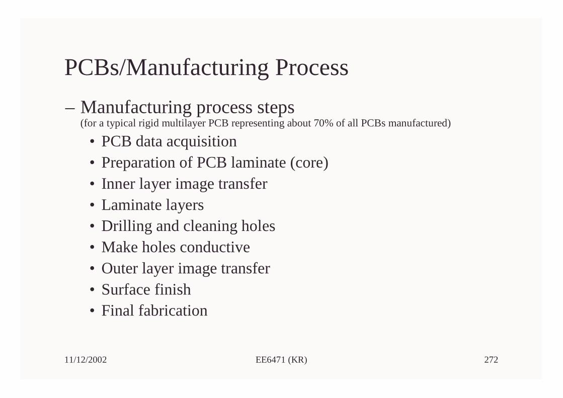
PCBs/Manufacturing Process
– Manufacturing process steps(for a typical rigid multilayer PCB representing about 70% of all PCBs manufactured)
• PCB data acquisition• Preparation of PCB laminate (core)• Inner layer image transfer• Laminate layers• Drilling and cleaning holes• Make holes conductive• Outer layer image transfer• Surface finish• Final fabrication

11/12/2002 EE6471 (KR) 273
PCBs/Manufacturing Process/Step 1– Step 1: PCB data acquisition
• Files transferred from PCB design house to PCB manufacturing facility:
– Gerber files, drill files, fabrication drawings
• File review by PCB manufacturer• Creation of PCB tooling
– Photo-tool for image transferImage created by PCB software is reproduced on film using laser photoplotters
– Drill files– Profile routing files
CNC route file
– All tooling is stepped and repeated for optimum utilisation of standard panels (24in x 18in)

11/12/2002 EE6471 (KR) 274
PCBs/Manufacturing Process/Step 2– Step 2: Preparation of PCB laminate (core)
• Dielectric material: Woven glass fiber or paperMaterial depends on the function of the PCB. Some materials perform better in some environments than others (heat, humidity). Some materials are more suitable for particular manufacturing processes (e.g. hole punching). Others again are chosen for electric properties (permittivity). Most widely used: FR4
• Coat/impregnate dielectric material with resin
• Copper foil is rolled or electrolytically deposited on the base laminate
• Core material is sheared to panel size
• Core material is cleaned mechanically and/or chemicallyRemoval of surface contamination required to promote subsequent adhesion of photoresist (PR)

11/12/2002 EE6471 (KR) 275
PCBs/Manufacturing Process/Step 3– Step 3: Inner layer image transfer
Purpose: Transfer circuit image to core through “print-and-etch” process
• Coat copper foils with photoresist (PR)Light-sensitive organic PR polymerizes when exposed to light. Polymerized PR will resist etching.
• Place phototool and expose to lightAfter expose, PR layer is developed. Polymerized areas remain, unexposed areas are washed away.
• EtchingSelectively remove exposed copper areas. Etching is performed with conveyorised equipment (etchant flood rinse, several water rinses). Common etchants: Acidic cupric chloride and alkaline ammoniacal.

11/12/2002 EE6471 (KR) 276
PCBs/Manufacturing Process/Step 4– Step 4: Lamination
• Cores are pinned in a stack with sheets of prepreg (b-stage) separating the copper layers. Outer layers are made with a foil of copper.
• Stack is pinned between two heavy metal plates creating a “book”.
• Book is put in a heated hydraulic press for about 2h.
Prepreg
Core
Prepreg
Core
Prepreg
Prepreg
Core
Outer Cu foil
Outer Cu foil
Temperature (175°C)Pressure (3000kg)Time (2h)
Prepreg is available in different styles with varying amounts of resin and glass fibers. This allows the manufacturer to control thickness between layers and thickness of the overall PCB.

11/12/2002 EE6471 (KR) 277
PCBs/Manufacturing Process/Step 5– Step 5: Drilling and cleaning
Purpose: Holes are drilled through PCB to interconnect layers (vias), and to allow the insertion of PTH components
• Drilling performed with CNC equipmentUsing drill files. Alternative methods to drilling exist (punching, laser).
• Multiple panels can be drilled togetherDrilling of complex boards can take several hours per load
• DesmearDesmear removes the melted resin smear
• EtchbackEtch glassfibers. Copper on the inner layersprotrude out into the barrel of the hole
• Panels are deburred/scrubbed afterdrilling

11/12/2002 EE6471 (KR) 278
PCBs/Manufacturing Process/Step 6– Step 6: Make holes conductive
PCB substrate is not conductive. Therefore a non-electrolytic deposition method is required. In a later process step, electroplating to the required thickness can be performed
• Process: Electroless copperElectroless copper is reliable but alternative methods exist. Electroless copper has some significant disadvantages (like exposure to formaldehyde, which is carcinogen).
• Electroless copper bathDeposits 75-125µIn of copper
• Constituents of electroless copper:Sodium hydroxide, formaldehyde, EDTA andcopper salt. Complex reaction catalysed bypalladium, formaldehyde reduces the copper ionto metallic copper.

11/12/2002 EE6471 (KR) 279
PCBs/Manufacturing Process/Step 7– Step 7: Outer layer image transfer
Most common process: Print, pattern plate, and etch
• Coat copper foils with photoresist (PR)
• Place phototool and expose to lightOuter layer phototools are positive images of the circuit. Circuit image is developed away exposing the copper. PR remaining on the panel will act as plating resist
• Pattern plating (copper electroplating)Outer layers will be plated to a thickness of 1.5mil (to ensure a minimum thickness of 1mil in the holes). Copper electroplating takes place in a copper sulfate bath.Plating is performed at roughly 30A/ft2. Platingduration is roughly 1h.
• Plate metallic etch resist
• Etching

11/12/2002 EE6471 (KR) 280
PCBs/Manufacturing Process/Step 8– Step 8: Surface finish
Purpose: Prevent copper oxidation. Facilitate solderability.
• Most popular surface finish process: SMOBC/HASL:SMOBC: Solder-mask-over-bare-copper. HASL: hot-air-solder-leveling
• Solder mask pre-clean (mechanical scrub)
• Application of solder maskPurpose of solder mask: Insulate those portions where no solder is required. Most popular mask type: LPI (liquid photoimageable).
• Application of fluxProvides oxidation protection. Affects heat transfer during solder immersion.
• HASLPanels are dipped into molten solder (237°C). Panels are then rapidly carried past jets of hot air. Exposed copper is coated with solder. Masked areas remain solder-free. Panels are then cleaned in hot water.

11/12/2002 EE6471 (KR) 281
PCBs/Manufacturing Process/Step 9– Step 9: Final fabrication
Mechanical features are added to the board (mounting holes, cutouts, etc)
• Routing done through CNC machines
• De-panelisation– Partial de-panelisation. Most of the circuit is routed out of the panel, but tabs
remain to hold the circuit in place. This allows the assembly machine to populate multiple boards at once. Afterwards, the circuit can be snapped or broken out of the panel. Such panels are called “breakaways”, “snaps”, or “arrays”.
– The alternative to partial de-panelisation is to have the panel V-scored. V-scoring is done through a thin rotating scoring blade that will route across the top and the bottom of the panel with about 30% of the thickness of the panel. V-scoring allows more circuits per panel (no spacing is required for routing bits).

11/12/2002 EE6471 (KR) 282
PCBs/Panels– PCB Boards are
fabricated in panels to minimise cost of PCB manufacturer and assembly manufacturer
– Typical panel dimensions are 18*24in (460x610mm)
– Overall board dimensions are kept much smaller than a full panel
11/12/2002 EE6471 (KR) 283
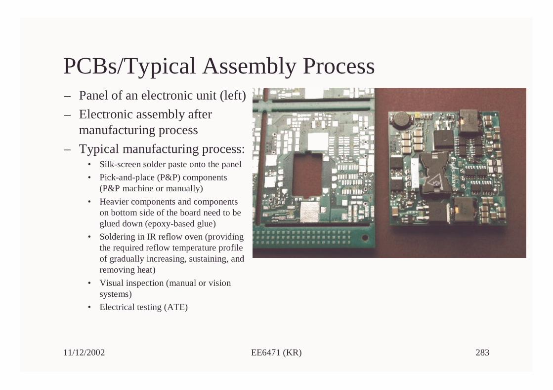
PCBs/Typical Assembly Process– Panel of an electronic unit (left)
– Electronic assembly after manufacturing process
– Typical manufacturing process:• Silk-screen solder paste onto the panel
• Pick-and-place (P&P) components (P&P machine or manually)
• Heavier components and components on bottom side of the board need to be glued down (epoxy-based glue)
• Soldering in IR reflow oven (providing the required reflow temperature profile of gradually increasing, sustaining, and removing heat)
• Visual inspection (manual or vision systems)
• Electrical testing (ATE)

11/12/2002 EE6471 (KR) 284
PCBs/Layout/Do’s and Don’ts– Do’s:
• Use (continuous) supply layers whenever possible. Keep connections to supply layers short
• Use SMT components wherever possible• Use filter components where required and possible• Place blocking capacitors as close as possible to supply pins of transient loads. Use
star-point connections at blocking caps.
Ground LayerSignal and Vcc Layer
74H
CT
xxx
74H
CT
xxx
CC
C
11/12/2002 EE6471 (KR) 285
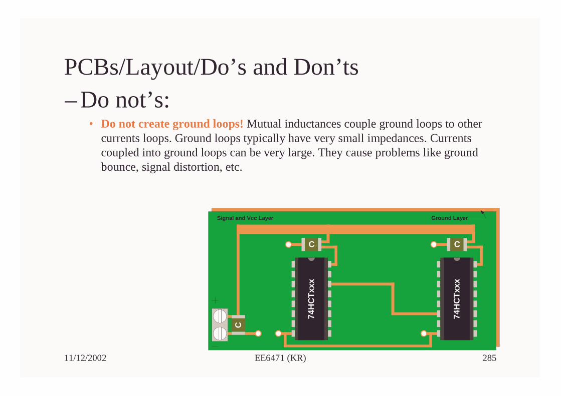
PCBs/Layout/Do’s and Don’ts– Do not’s:
• Do not create ground loops! Mutual inductances couple ground loops to other currents loops. Ground loops typically have very small impedances. Currents coupled into ground loops can be very large. They cause problems like ground bounce, signal distortion, etc.
Ground LayerSignal and Vcc Layer
74H
CT
xxx
74H
CT
xxx
CC
C

11/12/2002 EE6471 (KR) 286
PCBs/Layout/Do’s and Don’ts– Do not’s:
• Avoid discontinuities in grounds layers! High frequency return currents in ground layers follow the path with the least inductance. This path is usually directly underneath the signal trace. If there are discontinuities in the ground layer high frequency currents cannot flow underneath the signal trace. Large loop areas are created, and cause a variety of problems (ground bounce, cross-talk)
Ground LayerSignal and Vcc Layer
74H
CT
xxx
74H
CT
xxx
CC PTH connector
causing a slotin the ground
layer
C