principles of photoelectrochemical cells - springer
TRANSCRIPT

Chapter 2
Principles of Photoelectrochemical Cells
Roel van de Krol
2.1 The Photoelectrochemical Cell
Figure 2.1 shows a simplified energy diagram of a photoelectrochemical (PEC) cell
based on a single photoanode and a metal counter electrode. More complicated
configurations that involve photocathodes and/or more than one photoelectrode are
discussed at the end of this chapter. The main component of the PEC cell is the
semiconductor, which converts incident photons to electron–hole pairs. These
electrons and holes are spatially separated from each other due to the presence of
an electric field inside the semiconductor, the origin of which is discussed in
Sect. 2.5. The photogenerated electrons are swept toward the conducting back-
contact, and are transported to the metal counter-electrode via an external wire.
At the metal, the electrons reduce water to form hydrogen gas. The photogenerated
holes are swept toward the semiconductor/electrolyte interface, where they oxidize
water to form oxygen gas.
For an alkaline electrolyte, the reduction and oxidation reactions can be
written as1
4H2Oþ 4e� ! 2H2 þ 4OH� E0red ¼ �0:828 V vs: NHE (2.1)
4OH� þ 4hþ ! 2H2Oþ O2 E0ox ¼ �0:401 V vs: NHE: (2.2)
R. van de Krol (*)
Faculty of Applied Sciences, Department Chemical Engineering/Materials
for Energy Conversion and Storage, Delft University of Technology,
P.O. Box 5045, 2600 GA Delft, The Netherlands
e-mail: [email protected]
1 Note that the sign of the potential for the oxidation half-reactions is opposite from that usually
encountered in the literature, which usually lists these reactions as reduction reactions.
R. van de Krol and M. Gratzel (eds.), Photoelectrochemical Hydrogen Production,Electronic Materials: Science & Technology 102, DOI 10.1007/978-1-4614-1380-6_2,# Springer Science+Business Media, LLC 2012
13

For an acidic environment, the appropriate reactions can be obtained from (2.1)
and (2.2) by subtracting or adding the dissociation reaction of water into protons
and hydroxyl ions:
4Hþ þ 4e� ! 2H2 E0red ¼ þ0:000 V vs: NHE (2.3)
2H2Oþ 4hþ ! 4Hþ þ O2 E0ox ¼ �1:229 V vs: NHE: (2.4)
The Gibbs free energy change for the overall water splitting reaction is given by
the expression:
DG ¼ �nFDE: (2.5)
At standard temperature (298 K) and concentrations (1 mol/L, 1 bar), the electro-
chemical cell voltage DE of�1.229 V corresponds to a Gibbs free energy change of
+237 kJ/mol H2. This shows that the water-splitting reaction is thermodynamically
uphill. This is markedly different from the photocatalysis reactions that one
encounters in, e.g., photo-assisted degradation of organic pollutants, for which
the Gibbs free energy change is negative.
2.2 Semiconducting Photoelectrode Materials
Some of the key requirements for a semiconductor photoelectrode are efficient
absorption of visible light and good charge transport. It is often – though not
always – easy to determine these parameters from an experiment on a particular
material. Clearly, this approach becomes impractical if one wants to screen an
entire class of candidate photoelectrode materials. For such cases a more fruitful
Fig. 2.1 Illustration of a photoelectrochemical cell that consists of a semiconducting photoanode
and a metal cathode. The corresponding energy diagram is shown in the right
14 R. van de Krol
approach may be to calculate the electronic structure of a base material, and use this
to predict how the properties depend on, e.g., composition. While still far from
trivial, electronic structure calculations are now becoming more and more routine.
The required computing power and software are readily available, and the number
of electronic structure calculations reported in the literature, even by experimen-
tally oriented groups, increases rapidly. However, in order to use these spectra to
predict certain photoelectrode properties, one first needs to understand how chemi-
cal bonding between the atoms affects the electronic structure. Some of the main
principles are discussed below. In contrast to most standard textbooks, we empha-
size the properties of metal oxide semiconductors.
In most conventional semiconductors, such as Si and Ge, covalent bonding
dominates. In silicon, for example, the outer 3s and 3p orbitals combine to form
hybrid sp3 orbitals. Neighboring sp3 orbitals interact to form bonding and antibond-
ing combinations that form the valence and conduction bands of the material,
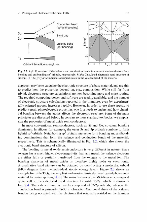
respectively. This is schematically illustrated in Fig. 2.2, which also shows the
electronic band structure of silicon.
The bonding in metal oxide semiconductors is very different in nature. Since
oxygen has a much higher electronegativity than any metal, the valence electrons
are either fully or partially transferred from the oxygen to the metal ion. The
bonding character of metal oxides is therefore highly polar or even ionic.
A qualitative band picture can be obtained by constructing a molecular orbital
(MO) diagram from the individual atomic energy levels. Figure 2.3 shows an
example for rutile TiO2, the very first and most extensively investigated photoanode
material for water splitting [2, 3]. The main features of the MO diagram correspond
quite well to the calculated band structure for rutile TiO2, which is shown in
Fig. 2.4. The valence band is mainly composed of O-2p orbitals, whereas the
conduction band is primarily Ti-3d in character. One could think of the valence
band as being occupied with the electrons that originally resided on the titanium
Fig. 2.2 Left: Formation of the valence and conduction bands in covalent semiconductors from
bonding and antibonding sp3 orbitals, respectively. Right: Calculated electronic band structure of
silicon [1]. The gray area indicates occupied states in the valence band of the material
2 Principles of Photoelectrochemical Cells 15

Fig. 2.3 Molecular orbital diagram of rutile TiO2 (after Stoyanov [4] and Fisher [5])
Fig. 2.4 Electronic band structure and density-of-states (DOS) of rutile TiO2. The black parts of
the DOS indicate completely filled bands. Adapted from Hoffmann [6], pp. 31, copyright Wiley-
VCH Verlag GmbH & Co. KGaA. Reproduced with permission
16 R. van de Krol

atoms, before they were transferred to the more electronegative oxygen during the
formation of the bond.2
It should be noted that such a “local” view is entirely inappropriate for covalent
semiconductors such as silicon, inwhich the electrons are completely delocalized over
the material. This local vs. delocalized view is a key feature that distinguishes metal
oxide semiconductors from their covalently bonded counterparts. The local character
of the energy bands inmetal oxides sometimes leads to ambiguous interpretations. For
example, “free” electrons in TiO2 are sometimes distinguished from Ti3+ species.
While such a distinction may be realistic at the surface of a material, where the
electronic structure is distorted due to a disruption of the lattice symmetry, it is not
obvious in the bulk inwhich the conduction band ismainly composed ofTi 3d orbitals.
While seemingly complicated, the electronic band structure can directly lead
to several important insights for photoelectrode materials. The first insight is
the nature of the optical transition, illustrated in more detail in Fig. 2.5. If the highest
point in the valence band is located at the same k-vector as the lowest point of the
conduction band, the optical transition does not require a change in crystal momen-
tum. Such a transition is called direct, and is indicated by a vertical line in the E–kdiagram. In contrast, indirect transitions do require a change in crystal momentum, as
illustrated in Fig. 2.5. Since photons carry very little momentum, indirect transitions
require absorption or emission of a phonon (i.e., a lattice vibration) and are much less
likely to occur. As a consequence, the absorption coefficient of indirect
semiconductors is much smaller than that of direct semiconductors – the difference
can be two orders of magnitude. This is why direct semiconductors, such as amor-
phous Si or CuInxGa1-xSe2 (CIGS) can absorb all incident light in just a few
micrometers, whereas crystalline (indirect) Si solar cells typically have a thickness
2 The valence band of a semiconductor is analogous to the highest occupied molecular orbital
(HOMO) in a molecule, whereas the conduction band is the solid state analogue of the lowest
unoccupied molecular orbital (LUMO).
Fig. 2.5 Optical transitions
in semiconductors with a
direct and an indirect
bandgap. The indirect
transition requires assistance
of a phonon with energy ho
2 Principles of Photoelectrochemical Cells 17

of ~300 mm.Metal oxides often have fairly horizontal-running E-k lines in their bandstructure (cf. Fig. 2.4), which sometimes obscures the direct vs. indirect nature.
The bandgap of a material can be determined from a measurement of the
absorption coefficient vs. wavelength. If the bottom of the conduction band and
the top of the valence band are assumed to have a parabolic shape, the absorption
coefficient (units: m�1) can be expressed as follows:
a ¼ A hn� Eg
� �mhn
: (2.6)
Here, A is a constant and m depends on the nature of the optical transition: m ¼ ½
for a direct bandgap, and m ¼ 2 for an indirect gap. From (2.6), extrapolation of a
plot of (ahn)1/2 vs. hn plot gives the indirect bandgap, while a plot of (ahn)2 vs.
hn yields the direct bandgap of the material. Such a plot is called a “Tauc plot” [7]
and is often encountered in the photoelectrochemistry and photocatalysis literature.
The second insight that can be obtained from the electronic band structure is the
mobility of charge carriers, which is related to the width of the conduction and
valence bands. For Si the bands are rather broad, spanning more than 10 eV. This is
a direct consequence of the extensive overlap of the sp3 orbitals on neighboring
atoms. More overlap between atomic wavefunctions results in broader bands and
easier transport of free charge carriers through the material. This can be quantified
via the curvature of the individual bands, which is directly related to the effective
mass and mobility of the charge carriers:
m� ¼ h2
@2E@k2
� � and m ¼ qtm�
: (2.7)
Wide bands that are strongly curved indicate a high charge carrier mobility. A high
mobility is especially desirable in photoelectrodes with an indirect bandgap. This is
because these materials require a large thickness to absorb all the incident light,
which means that photogenerated electrons and holes have to travel large distances
before reaching the interface.
Table 2.1 gives an overview of the room temperature charge carrier mobilities
of several semiconductors. What stands out are the small charge carrier mobilities for
the transition metal oxides. One reason for this is the fact that the 3d orbitals in
transition metals are fairly contracted, and show less overlap with neighboring atoms
than the s- and p-orbitals. One can also look at this from an electrostatic point of view.
The electrostatic interaction of a free electron with the cations surrounding it creates a
local lattice distortion. This distortion accompanies the electron when it moves
through the lattice, and is called a polaron. If the interaction is very strong, the polaroncan even become trapped at a particular lattice site. The electron can then only move
by thermally activated hopping, and its mobility will be very low. Similar
considerations apply to “free” holes in the valence band, which can form polarons
through electrostatic interaction with the surrounding oxygen ions. Charge transport
via polarons is believed to play an important role in, e.g., hematite (a-Fe2O3), which
will be discussed in more detail in Chap. 4.
18 R. van de Krol

The third piece of information that can be obtained from the electronic
band structure is the density-of-states (DOS). This is the number of allowed electronic
states per unit of energy interval. In E–k diagrams the k-values are equally spaced
along the k-axis, so the DOS can be readily estimated from the total length of the black
lines that run through a certain interval DE. As illustrated in Fig. 2.4 for TiO2, the
highest DOS occur at energies where the E–k curves are flat (horizontal). The DOSrepresentation not only allows one to quickly and easily identify the various bands and
band widths, but it also gives a rough impression of the optical transition probabilities
between various bands. This is because the total number of excitations per second is
proportional to the DOS at the occupied ground state (the initial state), multiplied by
the transition probability to the final state, lif. The latter is given by Fermi’s Golden
Rule, (2.8), and depends linearly on the DOS at the final (excited) state, gf:
lif ¼ 2ph
Mifj j2gf : (2.8)
In some cases, one can actually see certain features of the DOS reflected in the
optical absorption spectrum of the material.
2.3 Charge Carriers and Doping
Under equilibrium conditions (i.e., no illumination and no net current flow), the
concentration of free electrons in the conduction band and free holes in the valence
band is given by the following expressions:
n ¼ NC e� EC�EFð Þ=kT with NC ¼ 2
2pm�ekTh2
� �3=2
; (2.9)
Table 2.1 Charge carrier mobilities and effective masses at room temperature
Material
Mobility (cm2/V/s) Effective carrier masses (�me)
ReferencesElectrons Holes Electrons Holes
Si 1,500 450 [8]
GaAs 8,500 400 0.07 0.68 [8, 9]
CdS 340 50 0.19 0.8 [8, 9]
ZnO 200 180 0.24 0.45 [8, 9]
TiO2 (anatase) 2 � 10�3 a >10 0.8 [10, 11]
WO3 ~10 ~0.9 [12]
a-Fe2O3 0.1b 0.2c [13]
p-Cu2O 90 [14]
p-CuAlO2 10 [15]
p-SrCu2O2 0.46 [16]
p-CuMnO2 3.5 � 10�6 [17]aTheoretical estimatebAt 1,200 KcAt 1,400 K
2 Principles of Photoelectrochemical Cells 19

p ¼ NV e� EF�EVð Þ=kT with NV ¼ 22pm�hkT
h2
� �3=2
: (2.10)
Equations (2.9) and (2.10) are valid for both undoped and doped semiconductors.
They are, however, not valid when the Fermi level is less than ~3kT away from
either one of the band edges. Under these conditions, the semiconductor is degen-erate, and exhibits near-metallic behavior. The relationships for the effective
densities of states were derived from the (nearly) free electron model, and may
not be entirely accurate for transition metal oxides. Despite these limitations, (2.9)
and (2.10) are exceedingly useful for describing the behavior of semiconducting
photoelectrodes.
Semiconductors for practical applications are often doped, mainly with the aim
to improve the conductivity. In metal oxide photoelectrodes, shallow donors and
acceptors are almost always necessary because of the low intrinsic charge carrier
mobilities. The conductivity of the material is given by s ¼ neme + pemh, soincreasing n or p will compensate for a small value of me or mh. Examples of
donor-type dopants are Ti4+ on a Fe3+ site in Fe2O3, or phosphorus in silicon. The
extra valence electron introduced by the donor atom is loosely bound to the donor
nucleus, and can be excited to the conduction band where it then contributes to the
conductivity. Conversely, holes in acceptor-type dopants can be excited to
the valence band. Since a hole is equivalent to a missing electron, one can also
picture this as an electron being excited from the valence band into the energy level
of the acceptor species.
If the dopant level is within ~2kT of EC or EV, it will be (almost) fully ionized
at room temperature – this is referred to as a shallow dopant. For deep donors
and acceptors, the degree of ionization can be calculated with the following
equations:
NþDND
¼ 1
1þ gD e EF�EDð Þ=kT andN�ANA
¼ 1
1þ gA e EA�EFð Þ=kT : (2.11)
Here, ED and EA are the donor and acceptor energies and gA and gD are the
corresponding degeneracy factors that reflect the multiplicity of the energy
state [18]. Under the assumption that n ¼ NþD , the following useful expressions
relate the free electron concentration directly to the position of the donor level in the
bandgap [18]:
n ¼ Nz
2
ffiffiffiffiffiffiffiffiffiffiffiffiffiffiffiffiffi1þ 4ND
Nz
s� 1
!with Nz ¼ Nc
gD
� �e� EC�EDð Þ=kT (2.12)
20 R. van de Krol

An analogous expression can be obtained for acceptor-doped materials. The energy
levels for the various dopants are illustrated in Fig. 2.6. Deep dopants can act as
optically active centers or as catalytically active surface sites, as given in the
following paragraphs.
2.4 Defect Chemistry
Semiconducting photoelectrodes are almost always doped to improve their
properties. In most cases, the aim is to enhance the n- or p-type conductivity,
as described in Sect. 2.3. Certain dopants may enhance the optical absorption of
wide bandgap semiconductors [19], increase the minority carrier diffusion length
[20, 21], or enhance the catalytic activity at the surface of the semiconductor [22].
Other dopants adversely affect the properties, for example, by introducing midgap
bulk or surface states that act as recombination centers [23, 24].
In addition to foreign cation and anion dopants, native point defects are also
usually present in the material. Examples are vacancies, interstitials, or
substituents.3 These defects can have a similar influence on the optical, electrical,
and catalytic properties as dopants. They are formed by intrinsic defect-chemical
reactions, or by a change in the lattice stoichiometry due to exchange of, e.g.,
oxygen with the gas phase. Since virtually every defect affects the performance of
the material in some way, the ability to understand and predict the relationship
between dopants and defect concentrations is of paramount importance for design-
ing efficient photoelectrodes.
Fig. 2.6 Energy levels of
shallow and deep donors (SD,
DD) and acceptors (SA, DA)
in a semiconductor. Deep
donor or acceptor states can
also occur below or above
midgap, respectively. Midgap
states (RC) are often very
efficient recombination
centers and can be either
donor- or acceptor-like in
nature
3 An example of a native substituent is a site exchange of A and B cations in a ternary compound
such as ABxOy.
2 Principles of Photoelectrochemical Cells 21

2.4.1 Doping Binary Metal Oxides
In covalently bonded semiconductors, the introduction of dopants is fairly
straightforward since all lattice sites are similar to each other. This is even true for
a polar compound such as GaAs. In this material, Si can be incorporated on both Ga
and As lattice sites [25]. For ionically bondedmaterials the situation is quite different,
since the large electrostatic penalty prevents any exchange of anions and cations. This
puts certain restrictions on the incorporation of dopants, as given below.
The incorporation of dopants in metal oxides and other ionic materials can
be conveniently described with the so-called Kr€oger–Vink notation [26], which is
summarized in Fig. 2.7. For a more extensive description the reader is referred
to several excellent textbooks on this subject [27, 28]. When describing defect-
chemical reactions, one has to observe the conservation of mass and charge, just as
one would for any other chemical (half)reaction. What is different in the defect
chemistry of ionic solids is the conservation of lattice site stoichiometry. Forexample, if we dope Fe2O3 with zinc oxide, two zinc ions substitute for Fe, and
the two oxygen ions occupy two of the three oxygen sites in the Fe2O3 unit. This
means that the third oxygen site remains empty, resulting in an oxygen vacancy:
2ZnO�!Fe2O32Zn
=
Fe þ 2OxO þ V��O : (2.13)
Fig. 2.7 Diagram summarizing the key elements of the Kr€oger–Vink notation for point defects inionic solids. The formation of defects can be described with defect-chemical reactions and
corresponding equilibrium constants
22 R. van de Krol

Note that this is an irreversible reaction, since spontaneous demixing will not occur.
This means that one cannot define an equilibrium constant for a dissolutionreaction. Closer inspection shows that reaction (2.13) indeed fulfills the required
conservation of mass, charge, and lattice site stoichiometry.
One may try to get rid of the oxygen vacancy in reaction (2.13) by performing
the synthesis in an oxygen-rich atmosphere. In this case, both mass and lattice site
stoichiometry are conserved when adding the oxygen gas, which means that the
charge has to be balanced by the addition of a hole:
2ZnOþ 1=2O2(g)�!Fe2O32Zn
=
Fe þ 3OxOþh�: (2.14)
Note that the presence of a hole suggests p-type conductivity in Fe2O3. In many
cases, however, metal oxides remain n-type when acceptor-doped. If this is the
case, it is more appropriate to replace the hole with an electron on the left-hand side
of (2.14).
In (2.13) and (2.14) the charge of the aliovalent4 Zn dopant is compensated by an
ionic defect (V��O ) and an electronic defect (h•), respectively. To illustrate the
difference between these ionic and electronic compensation mechanisms in more
detail, consider Ti-doped Fe2O3. When subtracting the ionic compensation reaction
from the electronic one, we obtain
6TiO2�!3Fe2O36Ti�Fe þ 9Ox
Oþ3=2O2(g) + 6e=
(2.15)
6TiO2�!4Fe2O36Ti�Fe þ 12Ox
O þ 2V===
Fe (2.16)
3OxO þ 2V
===
Fe! 3=2O2(g)þ 6e
=
: (2.17)
This shows that the difference between two irreversible dissolution reactions canbe written as a reversible oxidation/reduction reaction. An important implication of
this is that the addition of a dopant is, by itself, not sufficient to enhance the
conductivity of a metal oxide photoelectrode: one also needs to ensure that
the equilibrium of reaction (2.17) lies at the right-hand side. The factors that affect
the equilibrium position are oxygen partial pressure, dopant concentration, and
temperature. The equilibrium constant of (2.17) is given by
K ¼ n6p3=2O2
[V===
Fe �2: (2.18)
4An “aliovalent” dopant has different charge than the ion that it replaces.
2 Principles of Photoelectrochemical Cells 23

From this, it is immediately clear that a low p(O2) favors electronic compensation.
Moreover, K is constant, so at constant p(O2) the factor n6=[V===
Fe �2 also remains
constant. This implies that at high dopant concentrations, ionic compensation will
dominate over electronic compensation. In otherwords, a plot of the conductivity as a
function of the Ti concentration will have its highest slope at low dopant
concentrations. Finally, we note that the entropy (DS) of (2.17) strongly increases
fromleft to right.SinceDG ¼ DH � TDS, electroniccompensation is favoredathigh
temperatures.
It is interesting to note that after subtracting the Fe2O3 Schottky reaction (see
Fig. 2.7) from (2.17), the standard oxygen reduction reaction for n-type oxides is
obtained:
OxO! V��O þ1=2O2(g) + 2e
=
: (2.19)
This reaction is of course valid for both doped and undoped metal oxides.
For doped metal oxides, the aliovalent metal ions influence the overall defect
concentrations via what is sometimes called the “First Law of Doping.” This law
simply states that adding an aliovalent dopant increases the concentration of defects
with opposite charges, and decreases the concentration of defects with charges of
the same sign.
The concentration of dopants in metal oxides is usually limited to 1–2% at most,
which corresponds to a concentration of ~1021 cm�3. Higher concentrations are notlikely to be effective, and may even lead to segregation of the dopant phase. If the
conductivity of a doped metal oxide photoelectrode is found to be too low, it may be
more effective to anneal it at high temperatures and under low p(O2) than to
increase the dopant concentration.
In (2.13)–(2.16), only one type of ionic defect was considered for each ionic
compensation reaction. In the case of ZnO-doped Fe2O3, the Zn acceptor could also
be compensated by a cation interstitial (Fe���i ) instead of an oxygen vacancy.
However, the higher charge of the interstitial Fe makes this energetically less
favorable. Similarly, oxygen interstitials instead of iron vacancies could compen-
sate the Ti donor in reaction (2.16), but in this case the large size of interstitial
anions prohibits this.5 In general, donor dopants are compensated by cation
vacancies or electrons, while acceptor dopants are compensated by anion vacancies,
cation interstitials, or holes. Which ionic defect is more likely to occur depends on
the crystal structure, the ionic radius, and the charge of the ion.
5Anion interstitials normally only occur in oxides with the fluorite structure, which can be viewed
as an fcc base lattice of cations in which the interstitial sites are occupied by anions.
24 R. van de Krol
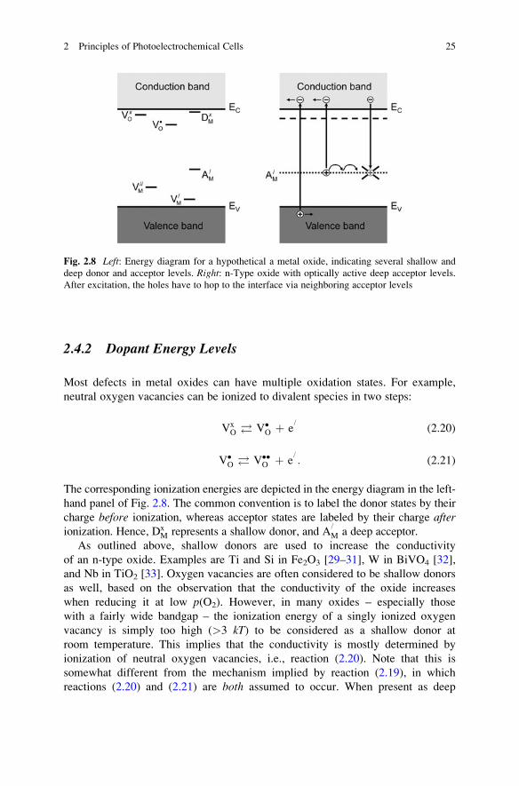
2.4.2 Dopant Energy Levels
Most defects in metal oxides can have multiple oxidation states. For example,
neutral oxygen vacancies can be ionized to divalent species in two steps:
VxO! V�O þ e
=
(2.20)
V�O ! V��O þ e=
: (2.21)
The corresponding ionization energies are depicted in the energy diagram in the left-
hand panel of Fig. 2.8. The common convention is to label the donor states by their
charge before ionization, whereas acceptor states are labeled by their charge afterionization. Hence, Dx
M represents a shallow donor, and A=
M a deep acceptor.
As outlined above, shallow donors are used to increase the conductivity
of an n-type oxide. Examples are Ti and Si in Fe2O3 [29–31], W in BiVO4 [32],
and Nb in TiO2 [33]. Oxygen vacancies are often considered to be shallow donors
as well, based on the observation that the conductivity of the oxide increases
when reducing it at low p(O2). However, in many oxides – especially those
with a fairly wide bandgap – the ionization energy of a singly ionized oxygen
vacancy is simply too high (>3 kT) to be considered as a shallow donor at
room temperature. This implies that the conductivity is mostly determined by
ionization of neutral oxygen vacancies, i.e., reaction (2.20). Note that this is
somewhat different from the mechanism implied by reaction (2.19), in which
reactions (2.20) and (2.21) are both assumed to occur. When present as deep
Fig. 2.8 Left: Energy diagram for a hypothetical a metal oxide, indicating several shallow and
deep donor and acceptor levels. Right: n-Type oxide with optically active deep acceptor levels.
After excitation, the holes have to hop to the interface via neighboring acceptor levels
2 Principles of Photoelectrochemical Cells 25
donor species, ionized oxygen vacancies may adversely affect the performance of
photoanodes by acting as recombination centers. If this is the case, their concentra-
tion can be kept low by doping with shallow donors, i.e., by using the First Law of
Doping.
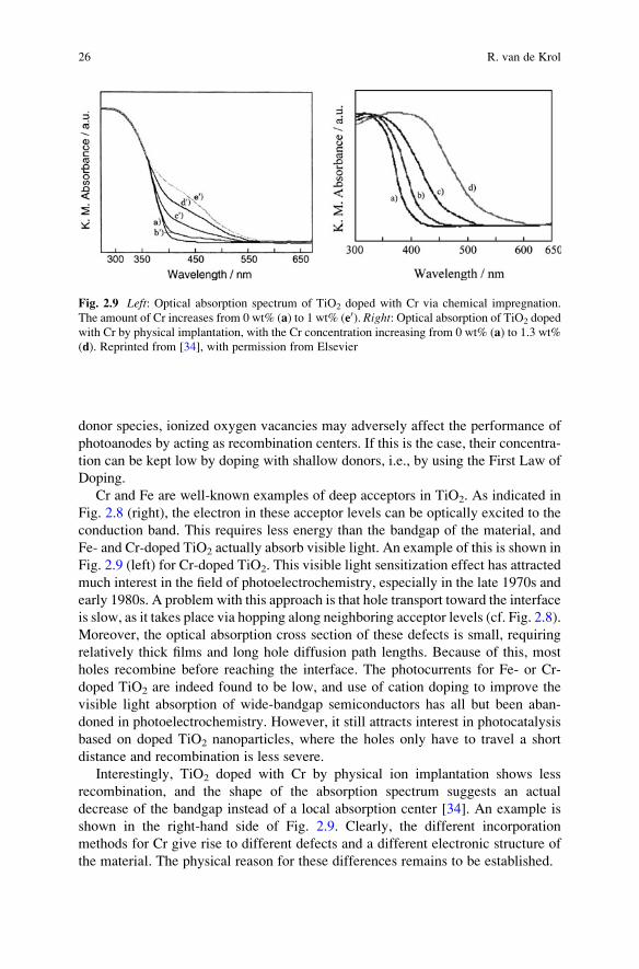
Cr and Fe are well-known examples of deep acceptors in TiO2. As indicated in
Fig. 2.8 (right), the electron in these acceptor levels can be optically excited to the
conduction band. This requires less energy than the bandgap of the material, and
Fe- and Cr-doped TiO2 actually absorb visible light. An example of this is shown in
Fig. 2.9 (left) for Cr-doped TiO2. This visible light sensitization effect has attracted
much interest in the field of photoelectrochemistry, especially in the late 1970s and
early 1980s. A problem with this approach is that hole transport toward the interface
is slow, as it takes place via hopping along neighboring acceptor levels (cf. Fig. 2.8).
Moreover, the optical absorption cross section of these defects is small, requiring
relatively thick films and long hole diffusion path lengths. Because of this, most
holes recombine before reaching the interface. The photocurrents for Fe- or Cr-
doped TiO2 are indeed found to be low, and use of cation doping to improve the
visible light absorption of wide-bandgap semiconductors has all but been aban-
doned in photoelectrochemistry. However, it still attracts interest in photocatalysis
based on doped TiO2 nanoparticles, where the holes only have to travel a short
distance and recombination is less severe.
Interestingly, TiO2 doped with Cr by physical ion implantation shows less
recombination, and the shape of the absorption spectrum suggests an actual
decrease of the bandgap instead of a local absorption center [34]. An example is
shown in the right-hand side of Fig. 2.9. Clearly, the different incorporation
methods for Cr give rise to different defects and a different electronic structure of
the material. The physical reason for these differences remains to be established.
Fig. 2.9 Left: Optical absorption spectrum of TiO2 doped with Cr via chemical impregnation.
The amount of Cr increases from 0 wt% (a) to 1 wt% (e0). Right: Optical absorption of TiO2 doped
with Cr by physical implantation, with the Cr concentration increasing from 0 wt% (a) to 1.3 wt%
(d). Reprinted from [34], with permission from Elsevier
26 R. van de Krol

2.4.3 Defect Equilibria
If all the defect formation energies and/or equilibrium constants are known, the
concentration of all the defects in a material can be calculated. As an example, we
briefly consider the case for a hypothetical M2O3 photoanode doped with X4+. Let
us assume that X substitutes for the metal (as opposed to occupying an interstitial
site), that Schottky disorder dominates in M2O3, and that the material is n-type
(n � p). We furthermore assume that fully ionized oxygen vacancies are deep
donors and can easily trap an electron, whereas singly ionized oxygen vacancies are
shallow donors. We can then write the following defect equations and equilibrium
constants:
2XO2�!M2O3
2X�M þ 3OxO þ 1=2O2(g) + 2e
=
(2.22)
0 ! 3V===
M þ 2 V��O KS ¼ [V===
M �3[V��O �2 (2.23)
0 ! e=þ h� Ke ¼ np (2.24)
OxO! V��O þ 1=2O2ðgÞ þ 2e
=
KR¼ n2[V��O �p1=2O2(2.25)
V�O ! V��O þ e=
Ki ¼ ½V��O �n
[V�O�: (2.26)
No equilibrium constant is defined for the dissolution reaction, since it is irrevers-
ible. Note that we have chosen to write the electronic compensation form of the
dissolution reaction; we could have just as easily have chosen the ionic compensa-
tion reaction. As we saw before, they are related through reduction reaction (2.25)
and are therefore not independent of each other.
We now have four equilibrium equations and five unknown variables ([V===
M �,[V��O �, [V�O�, n, p). The missing equation is the electroneutrality equation:
3[V===
M � þ n ¼ 2½V��O � þ ½V�O� þ p (2.27)
This system of nonlinear algebraic equations can be numerically solved with
a computer, or one can find analytical solutions by simplification of (2.27) into
six separate Brouwer regimes. Each Brouwer regime is characterized by a single
dominant positive defect and a single dominant negative defect. While finding
the right order of the different Brouwer regimes as a function of p(O2) may
pose a bit of a challenge, one can derive all defect concentrations as a function of
p(O2) by hand and plot these in a so-called “Brouwer diagram” (sometimes also
2 Principles of Photoelectrochemical Cells 27

called a “Kr€oger–Vink diagram”). An example of such a diagram is shown in
Fig. 2.10. Such diagrams can be very helpful in the study of metal oxide
photoelectrodes since they immediately reveal which defects dominate in a certain
p(O2) regime.
2.4.4 Doping of Complex Metal Oxides
Since only very few binary oxides show promise as photoelectrodes for water
splitting, most notably WO3 and Fe2O3, PEC research activities have now partly
shifted toward ternary and more complex metal oxides (see, e.g., Chaps. 5 and 6).
One of the best known examples is BiVO4, which is an n-type semiconductor with a
Fig. 2.10 Brouwer diagram for a metal oxide MO doped with a donor species (FO2, with F being a
metal ion) in which Schottky disorder dominates. Also indicated are defect associates (marked by
an asterisk), clusters of defects that are held together by electrostatic forces. Such clusters are
known to form at high defect concentrations. From [27], with permission
28 R. van de Krol

bandgap of ~2.4 eV [35, 36]. Recent results from the author’s laboratory show
that electron transport limits the performance of undoped BiVO4 photoanodes [32].
To improve this, one can dope BiVO4 with tungsten in order to increase the
concentration of free electrons. Tungsten has a valence of 6+ and a crystal ionic
radius of 42 pm. It will therefore be a substitute for tetrahedrally coordinated V5+,
which has a slightly smaller ionic radius (36 pm).6 When W6+ substitutes for V5+,
one might expect the positive charge to be compensated by free electrons, thereby
increasing the conductivity. However, there is a minor complication: the compen-
sating negative charge is already provided in the form of Bi vacancies. Since
tungsten only occupies sites on the vanadium sublattice, the formation of Bi
vacancies is necessary in order to preserve lattice site stoichiometry. This leads to
the following electronic compensation reaction:
WO3þ1=2O2ðgÞþ2e=�!BiVO4V
===
Bi þW�V þ 4OxO: (2.28a)
According to (2.28a), W-doping actually decreases the conductivity of n-type
BiVO4, which is a rather unexpected (and undesired) result. It is also possible to
write an alternative reaction in which lattice site stoichiometry is preserved by the
segregation of vanadium out of the BiVO4 in the form of V2O5:
2BiVO4 þ 2WO3�!2BiVO42BixBi þ 2W�V þ V2O5 þ Ox
Oþ1=2O2ðgÞ þ 2e=
: (2.28b)
This avoids the need for highly charged cation vacancies, and the W dopant is
now indeed charge-compensated by the desired free electrons. Which reaction
actually occurs – (2.28a) or (2.28b) – depends on the energy required to form a
triply charged Bi vacancy vs. the energy required to form a second phase.
It should be realized that reactions (2.28a) and (2.28b) are both unfavorable from
an energetic point of view. In one case a highly charged defect has to be formed,
while in the other case a second phase has to segregate out. This leads to an
important general observation for ternary – and more complex – metal oxides:
doping these materials by simply dissolving a binary oxide is difficult to achieve in
practice. An elegant solution for this is to co-dope the BiVO4 with equal amounts of
W and Bi:
2WO3 þ Bi2O3�!2BiVO42BixBi þ 2W�V þ 8Ox
Oþ1=2O2(g)þ 2e=
: (2.29)
Co-doping can be easily achieved by having a small excess of Bi over V during the
synthesis of the material, so that [Bi] + [W] ¼ [V]. This is a well known and
powerful trick to increase the solubility of binary oxides in ternary oxides in
order to incorporate donor- or acceptor-type dopants.
6 Note that the octahedrally coordinated Bi sites (103 pm) are clearly too large for W, and would
cause the W6+ to “rattle,” which is energetically very unfavorable.
2 Principles of Photoelectrochemical Cells 29

2.5 Space Charges and Band Bending
One of the key features of a semiconductor is the presence of a built-in electric field,
or space charge. In devices for solar energy conversion, this field is responsible forthe efficient separation of the photogenerated electrons and holes, thereby
preventing recombination. The field is present near the surface or interface of a
semiconductor, and is formed by the transfer of charges from the semiconductor
bulk across its interface. The reason for charge transfer and the field induced by the
remaining charges inside the semiconductor is described below.
2.5.1 Origin of the Space Charge Layer
In most semiconductor textbooks, the formation of a space charge is explained by
a semiconductor being brought into contact with a metal or another semiconductor
[8, 37]. When both materials have different Fermi levels (i.e., electrochemical
potentials), charge is transferred between them until an equilibrium is established.
In metal oxide semiconductors, a built-in electric field can even be formed at the
surface without making contact with another solid. This is illustrated in the sche-
matic diagram of Fig. 2.11. When a metal oxide is exposed to air, water molecules
from the air can dissociatively adsorb at its surface, resulting in -OH surface
termination. Since the symmetry of the bulk lattice is broken at the surface, these
-OH groups form electronic surface states within the bandgap of the semiconductor.
The energy levels of these surface states are below the conduction band minimum,
and free electrons from the bulk will occupy these levels. The ionized donors from
which the free electrons originated will of course stay behind in the bulk, where
they form a positive space charge. An electric field now forms, and the charge
transfer from bulk to surface will continue until the potential barrier becomes too
large for bulk electrons to cross. At this point, a dynamic equilibrium establishes at
which no net electron transport takes place. The Fermi level at the surface is then
located somewhere halfway the DOS of the surface state.
2.5.2 Potential Distribution in The Depletion Layer
The potential distribution and width of space charge depend on the amount of
charges transferred to the surface and the density of shallow donors in the material,
ND. Quantitative expressions for these relationships are indispensible in PEC
research, and to understand where they come from, we derive them below. The
geometry of the problem and the relevant parameters are schematically illustrated
in Fig. 2.12. The starting point for the derivation is Poisson’s law, which relates the
potential to the net amount of charge:
d2fdx2¼ �dx
dx¼ �rðxÞ
e0er: (2.30)
30 R. van de Krol

Fig. 2.11 Simplified illustration of the formation of a space charge region (SCR) at a metal oxide
semiconductor surface when exposed to (humid) air
Fig. 2.12 Illustration of band bending at the surface of a n-type semiconductor in depletion. The
“+” markers just below the conduction band represent the ionized donor species, whereas the “�”markers just above the conduction band level represent the free electrons. The potential in the bulk
of the semiconductor is chosen as zero
2 Principles of Photoelectrochemical Cells 31

Here, xwas chosen as a symbol for the electric field to avoid confusion with symbol
E for energy. The total charge density in the space charge is given by the concen-
tration of free electrons, n, plus the concentration of ionized donors, NþD :
rðxÞ ¼ e NþD � n� �
: (2.31)
The concentration of free electrons is given by the distance between the
conduction band minimum and the Fermi level, cf. (2.9). Inside the SCR, this
distance is modified by the band bending f(x), which leads to the following
expression for n:
nðxÞ ¼ NC e�ðEC�EF�efðxÞÞ=kT ¼ nb e
efðxÞ=kT : (2.32)
Note that the energy of an electron is related to its potential by E ¼ �ef and that
the potential in the bulk of the semiconductor is conveniently chosen as zero (see
Fig. 2.12). Since the bulk is electrically neutral, its electron concentration, nb, must
be equal to the number of ionized donors. The latter are assumed to be fully ionized,
so that NþD ¼ ND ¼ nb. Combining this with (2.31) and (2.32), the total charge
density at point x can be written as
rðxÞ ¼ eND 1� eefðxÞ=kT� �
: (2.33)
The combination of (2.30) and (2.33) cannot be readily solved due to the implicit
dependence on f(x). Fortunately, there is an elegant way around this by taking the
derivative of the square of the electric field [38]. Using this with (2.30) yields:
d x2� �dx¼ 2x
dxdx¼ 2x
rðxÞe0er¼ �2 rðxÞ
e0er
dfdx
: (2.34)
Since there is a one-to-one correspondence between f and x, we can now switch the
independent variable from x to f and rewrite (2.34) as
x2 ¼ðfðxÞ0
�2 rðfÞe0er
df: (2.35)
The total net charge between the (neutral) bulk and point x in the space charge
can be related to the electric field at point x via the integral form of Gauss’ law:
x ¼ Q
e0erA: (2.36)
32 R. van de Krol

Here, A is the surface area of semiconductor. Combining (2.35) and (2.36) gives:
Q ¼
ffiffiffiffiffiffiffiffiffiffiffiffiffiffiffiffiffiffiffiffiffiffiffiffiffiffiffiffiffiffiffiffiffiffiffiffiffiffiffiffiffiffiffiffi�2e0erA2
ðfðxÞ0
rðfÞ df:
vuuut (2.37)
This equation provides a convenient starting point for further analysis of the space
charge. It is generally applicable and can also deal with nonhomogeneous doping
profiles and deep donors/acceptors. Here, we limit ourselves to homogeneously
distributed shallow donors, for which the charge density is given by (2.33).
The total amount of charge in the SCR can now be obtained by combining (2.33)
and (2.37) and integrating between f ¼ 0 and f ¼ fS ¼ �fSC :
QSC ¼
ffiffiffiffiffiffiffiffiffiffiffiffiffiffiffiffiffiffiffiffiffiffiffiffiffiffiffiffiffiffiffiffiffiffiffiffiffiffiffiffiffiffiffiffiffiffiffiffiffiffiffiffiffiffiffiffiffiffiffiffiffiffiffiffiffi�2e0erA2
ð�fsc
0
eND 1� eef=kTð Þ df
vuuut
¼ffiffiffiffiffiffiffiffiffiffiffiffiffiffiffiffiffiffiffiffiffiffiffiffiffiffiffiffiffiffiffiffiffiffiffiffiffiffiffiffiffiffiffiffiffiffiffiffiffiffiffiffiffiffiffiffiffiffiffiffiffiffiffiffiffiffiffiffiffiffiffiffiffiffiffiffiffiffi2e0ereNDA2 fSC þ
kT
ee�efSC=kT � kT
e
� �s: (2.38)
Under normal PEC operating conditions, the potential drop across the space charge
is at least 0.1 V, and the previous result can be simplified to
QSC ¼ffiffiffiffiffiffiffiffiffiffiffiffiffiffiffiffiffiffiffiffiffiffiffiffiffiffiffiffiffiffiffiffiffiffiffiffiffiffiffiffiffiffiffiffiffiffiffiffi2e0ereNDA2 fSC �
kT
e
� �s: (2.39)
The total amount of charge is related to the depletion layer thickness via
QSC ¼ eNDAW (2.40)
which leads to the following widely used expression for the space charge width:
W ¼ffiffiffiffiffiffiffiffiffiffiffiffiffiffiffiffiffiffiffiffiffiffiffiffiffiffiffiffiffiffiffiffiffiffiffiffi2e0ereND
fSC �kT
e
� �s: (2.41)
Although this important result was derived for n-type semiconductors, it is also
valid for p-type materials if ND is replaced with the shallow acceptor density, NA.
To get an idea of typical numbers, Fig. 2.13 shows the calculated depletion layer
width for a-Fe2O3 as a function of fSC for various dopant densities. Typical values
range between 5 and 500 nm. The total amount of charge in the depletion layer has
to be compensated by a sheet of oppositely charged species (e.g., trapped electrons)
at the surface of the material. As can be seen in the right-hand part of Fig. 2.13, less
2 Principles of Photoelectrochemical Cells 33

than 1% of a monolayer7 of adsorbed surface charges is already more than sufficient
to induce a significant space charge layer in the material.
The actual values of the dopant density and the depletion layer width can be
determined by impedance measurements. Under certain conditions one can extract
the differential capacitance of the space charge, CSC, from the total impedance of
the system. CSC can be derived by differentiating (2.39) with respect to fSC:
1
C2SC
¼ dQSC
dfSC
� ��2¼ 2
e0ereNDA2fSC �
kT
e
� �: (2.42)
This is the so-called “Mott–Schottky” equation. Typical values for CSC are
10–1,000 nF/cm2. By plotting 1/CSC2 as a function of the applied potential, the
donor density of the semiconductor can be determined.
2.5.3 Deep Depletion, Inversion, and Accumulation Layers
In addition to the depletion layer, other types of space charges can also form in a
semiconductor. These are illustrated in Fig. 2.14. If the number of adsorbed
negative (positive) surface charges increases beyond a certain number for an n-
type (p-type) semiconductor, the Fermi level crosses the middle of the bandgap and
the surface region becomes p-type (n-type). This is called an inversion layer.
Formation of an inversion layer is not always possible; if the dominant charge
carriers in the inversion layer are annihilated faster than they are (thermally)
7 1 monolayer (ML) corresponds to ~1015 atoms/cm2.
Fig. 2.13 Left: Depletion layer width as a function of potential drop across the space charge (fSC)
and (shallow) dopant density. Right: Corresponding amount of adsorbed surface charges needed to
compensate the charges in the depletion layer. The data are calculated for a-Fe2O3 assuming a
static dielectric constant of 25 [39, 40]
34 R. van de Krol

generated, no free charge carriers are present and the surface remains insulating.
A deep depletion layer is then formed. Deep depletion layers are fairly common in
photoelectrode materials with a relatively large bandgap (>2 eV) because genera-
tion of minority carriers is difficult in these materials. They can also be formed in
the presence of surface-adsorbed species that consume the minority carriers through
fast oxidation or reduction reactions. An accumulation layer can form when an
excess of positive (negative) charges is adsorbed at the surface of an n-type (p-type)
semiconductor. To compensate these surface charges, free majority carriers will
accumulate near the surface, forming the accumulation layer.
Whereas the charge density in a depletion layer is limited by the concentration of
ionized dopant ions (usually 1016–1018 cm�3), the concentration of electronic
Fig. 2.14 Different types of space charges in n- and p-type semiconductors. A normal depletion
layer contains only ionized donors or acceptors. An inversion layer is formed when the Fermi level
crosses the midgap energy, and the minority carriers outnumber the majority carriers in a thin layer
at the surface. When these minority carriers are consumed faster than they are generated, a deep
depletion layer forms; under these conditions the surface is not in thermal equilibrium and the
Fermi level is not well defined in this region. In an accumulation layer, the adsorbed surface
charges are compensated by majority charge carriers that accumulate at the surface
2 Principles of Photoelectrochemical Cells 35

charge carriers is limited by the effective density of states and can reach values
up to ~1020 cm-3. Due to this high density, the widths of the accumulation layer and
the thin inverted surface region for an inversion layer are usually in the order of
1–15 nm, i.e., much thinner than that of a typical depletion layer. The width of a
deep depletion layer can be evaluated by the same expression as that for a normal
depletion layer. The expressions for the thickness of the inversion and accumulation
layers are seldom necessary in photoelectrochemical water splitting – they can be
found in the literature [8, 41]. Finally, it should be noted that all four space charge
layers can, in principle, be formed by applying an external potential to a semicon-
ductor photoelectrode. The effect of applying a potential is discussed in the next
section.
2.6 The Semiconductor–Liquid Junction
When a metal oxide semiconductor is exposed to humid air, hydroxylation of the
surface occurs as described in Sect. 2.5.1. A slightly more complicated situation
arises when the semiconductor is immersed in an aqueous solution. Depending on the
pH of the solution, specific adsorption of protons and/or hydroxide species affect
the charge distribution at the semiconductor/electrolyte interface, and thereby also
the potential distribution. Analysis of the potential distribution allows us to construct
an energy diagram of the complete PEC cell. This diagram is indispensible for a
thorough understanding of the thermodynamics of PEC devices, as well as the charge
transfer processes that make it work.
2.6.1 Surface Hydroxylation
When a semiconductor is immersed in an aqueous solution, H+ and OH� ions in thesolution will continuously adsorb and desorb from the surface. A dynamic equilib-
rium will be established, which can be described by the following protonation and
deprotonation reactions:
M� OH! ka
MO� + Hþaq (2.43)
M� OH + Hþaq! kb
M� OHþ2 : (2.44)
The equilibrium of these reactions depends on the pH of the solution and the
Brønsted acidity of the surface. Depending on these conditions, the net total charge
adsorbed at the surface will be positive, zero, or negative. The pH at which the net
adsorbed charge is zero is called the point of zero charge (PZC) of the semiconductor.
36 R. van de Krol

Note that the reactions (2.43) and (2.44) are only appropriate for hydroxylated
semiconductor surfaces that are amphoteric,8 which is indeed true for most metal
oxide photoelectrodes.
2.6.2 The Semiconductor/Electrolyte Interface
The structure of the semiconductor/electrolyte interface is illustrated in Fig. 2.15.
The charges at the surface consists of electrons (or holes) trapped in surface states,
plus the specifically adsorbed ions described in reactions (2.43) and (2.44). The
counter charges are provided by ionized donors or acceptors in the solid, plus an
accumulation of oppositely charged ions in the solution. Due to the large dipole
moment of water, all ions in the solution are surrounded by a solvation cloud of
water molecules. This cloud prevents them from approaching the surface closer
than a few Angstr€oms (see Fig. 2.15). The region between the specifically adsorbed
ions and the closest ions in the solution is called the Helmholtz layer. The potentialdrop across this layer is given by
8 “Amphoteric” means that the semiconductor surface can either donate or accept a proton, i.e., it
can act both as a Brønsted acid and as a Brønsted base.
Fig. 2.15 Schematic model of the semiconductor/electrolyte interface and the Helmholtz layer.
The inner Helmholtz plane (ihp) consists of H+ and OH� ions that are specifically adsorbed at the
semiconductor surface. The outer Helmholtz plane (ohp) marks the distance of closest approach
for ions still in the solution. The distance d is only a few Angstr€oms due to the solvation sheet of
water molecules surrounding each ion
2 Principles of Photoelectrochemical Cells 37

VH ¼ xd ¼ QSd
e0er: (2.45)
The width of the Helmholtz layer is ~2–5 A, and on such a small length scale the
dielectric constant of water is estimated to be ~6, i.e., much smaller than its bulk
value of 80 [42]. For a surface charge of QS ¼ 1013 cm-2 (Fig. 2.13), the potential
drop across the Helmholtz layer is typically in the order of ~0.1–0.5 V. The
Helmholtz capacitance is 10–20 mF/cm2 [42].
During adsorption and desorption from the semiconductor surface, the ions gain
or lose energy while crossing the Helmholtz layer due to the Helmholtz voltage.
This leads to the following equilibrium constants for reactions (2.43) and (2.44):
½M� O��½Hþaq�[M� OH]
¼ ka ¼ exp�ðDGa � eVHÞ
kT
� �(2.46)
½M� OHþ2 �[M� OH][Hþaq�
¼ kb ¼ exp�ðDGb þ eVHÞ
kT
� �: (2.47)
Making use of the fact that VH ¼ 0 and [M–O�] ¼ [M–OH2+] at pH ¼ PZC, the
Gibbs free energies can be eliminated to yield the following expression for VH:
VH ¼ 2:3kT
elog
½M� O��[M� OHþ2 �� �1=2
þ 2:3kT
eðPZC� pHÞ: (2.48)
As seen above, the excess charge at the surface is usually very small, in the order of
1% of a monolayer or less. Hence, [M–O�] � [M–OH2+] and (2.48) can be
simplified to
VH ¼ 2:3kT
eðPZC� pHÞ: (2.49)
This important result shows that the Helmholtz potential changes with -59 mV
(2.3kT/e) per pH unit at 25C.
2.6.3 The Band Diagram
Now we understand the structure of the semiconductor/electrolyte interface, we can
draw a detailed band diagram for a complete PEC cell. An example is shown in
Fig. 2.16 for a cell composed of a n-type photoanode and a metal counter electrode.
As usual, the y-axis represent the energy of an electron at a certain point x in
the cell. The energy of an electron in vacuum at infinite distance is chosen as a
reference. It is important to note that the vacuum level bends in the presence of an
38 R. van de Krol

electric field, i.e., it follows the potential gradients that are present in the PEC cell.
This may seem a bit odd for a “reference” energy, but it is a consequence of the
convention that the electrochemical potential (or Fermi energy) of the electrons is
drawn as a constant value when the system is in equilibrium.
We now take a closer look at the electrolyte phase in Fig. 2.16. The energy of
a redox couple in an electrolyte with respect to the vacuum level (efR*) is not
accurately known. Theoretical and experimental estimates place the H2/H+ standard
redox energy between 4.3 and 4.85 eV below Evacuum [43]. Usually a value of
4.5 eV is taken, but it should be realized that this value has an uncertainty of a few
tenths of an eV; Bockris suggested a value of (4.6 0.2) eV [42]. The value
recommended by IUPAC is (4.44 0.02) eV [44]. The vacuum level has been
drawn as a horizontal line in the electrolyte, since no electric field is assumed to be
present in this phase. This is a realistic assumption for most water splitting
applications because highly concentrated electrolytes are used in order to avoid
Ohmic voltage losses. For very low electrolyte concentrations (<0.1 M), there
may be insufficient ions available at the outer Helmholtz plane to compensate all
the adsorbed charges at the semiconductor surface. These charges are then
compensated in a region that extends much beyond the outer Helmholtz plane,
the so-called Gouy layer. The potential distribution in this layer resembles that of a
SCR in a semiconductor and is described by the Gouy–Chapman theory. Since the
Gouy layer is rarely relevant for solar water splitting applications, we refer the
reader to the literature for a more detailed description [42].
Fig. 2.16 Energy diagram for a PEC cell based on a n-type semiconductor and a metal counter
electrode. The vacuum energy level is taken as a reference; this is the energy of an electron in
vacuum at infinite distance. The electron affinity (w) and ionization energy (IE) are materials
constants, whereas the semiconductor work function (fS) also depends on the distance to the
surface. Note that a Helmholtz layer is also present at the metal/electrolyte interface
2 Principles of Photoelectrochemical Cells 39

The key parameters for the semiconductor are the band positions, the
amount of band bending, and the difference between EC and EF. The latter depends
on the free electron concentration in the bulk ( ¼ NþD � N�A) and can be calculated
by (2.9). The energy diagram directly showswhether a certain reduction or oxidation
reaction at the semiconductor surface is thermodynamically possible. In
the example of Fig. 2.16, photogenerated holes will be able to oxidize water if the
H2O/O2 redox energy is positioned above the top of the valence band. Similarly,
only electrons with an energy above the redox energy can reduce the corresponding
species in the electrolyte. By measuring the potential (i.e., the Fermi level) of
the semiconductor with respect to that of a reference electrode, its reduction
or oxidation power can be determined. The advantage of using a reference
electrode for this is that the measured potential difference does not depend on the
amount of current that flows through the cell. In contrast, the potential difference
between the semiconductor and the metal counter electrode depends on VH at the
metal electrode (i.e., the overpotential), which depends on the current in an
unknown way.
Because of the high concentration of free electrons in the metal counter elec-
trode, the SCR inside the metal is extremely thin (~1 A) and can therefore be
ignored. The structure of the Helmholtz layer at the metal/electrolyte interface is
similar to that described for the semiconductor, and the capacitance is also in the
order of 10–20 mF/cm2. As already hinted in the previous paragraph, the potential
drop across the Helmholtz layer depends on the kinetics of electron transfer across
the interface. This is because any overpotential applied to a metal electrode must
fall across the Helmholtz layer. This is quite different from the case of an external
potential applied to a semiconductor electrode, which is discussed in the next
section.
2.6.4 Applying A Bias Potential
The operation of a PEC cell can be influenced by applying an external bias potential
to the semiconductor. When the bias is applied with respect to a reference electrode,
the potential difference will be distributed over the space charge layer and the
Helmholtz layer. These layers act as two capacitances in series [41]:
1
Ctot
¼ 1
CSC
þ 1
CH
: (2.50)
Both layers have the same charge Q associated with them (this is the charge that is
located at the inner Helmholtz plane), and since C ¼ Q/V the potential distribution
is given by
DVSC
DVH
¼ CH
CSC
: (2.51)
40 R. van de Krol

Because CH � CSC (see above), any change in applied bias will fall across the
depletion layer of the semiconductor.9 This important conclusion is illustrated in
Fig. 2.17. As shown in this figure, applying a positive bias to an n-type semicon-
ductor results in an increase of the depletion layer. For a p-type semiconductor, a
negative bias is required to increase the depletion layer. The ability to change the
band bending in a semiconductor electrode is immensely useful in the characteri-
zation of these materials, as we see in later chapters.
2.6.5 pH Dependence of The Band Edges
While VH is not affected by the applied bias potential, it does depend on the pH of
the solution as described by (2.49). This means that the positions of the band edges
shift with�59 mV per pH unit with respect to the redox potentials in the electrolyte.
At first sight, this seems to be a very useful property: if reduction of a certain
species is not possible because the conduction band is too low in energy, one might
consider increasing the pH toward more alkaline values to make VH more negative
and raise EC with respect to Eredox (a consequence is of course that this also
increases EV, so it reduces the oxidation power of the semiconductor). Unfortu-
nately, this strategy does not help for water splitting because the reduction and
oxidation potentials of water also depend on the pH via the Nernst equation. For
reactions (2.1) and (2.2) in Sect. 2.2, the Nernst equations read:
9Note that in highly doped semiconductors (>1019 cm�3) and metals, CSC can exceed CH so that
any change in the applied potential will fall across the Helmholtz layer instead of the depletion
layer.
Fig. 2.17 Effect of applying a bias voltage (VA) to an n-type semiconductor electrode. Any
change in applied potential falls across the space charge layer, whereas VH remains constant. In the
picture on the left, a positive potential is applied to the semiconductor. When a sufficiently
negative bias is applied, the band bending can be reduced to zero (right)
2 Principles of Photoelectrochemical Cells 41

Ered ¼ E0red �
RT
4Fln
p2H2
½Hþ�4 !
¼ E0red �
2:3RT
Flog p
1=2H2
� �þ pH
� �(2.52)
Eox ¼ E0ox þ
RT
4Fln pO2
½Hþ�4� �
¼ E0ox þ
2:3RT
Flog pO2ð Þ � pHð Þ: (2.53)
Hence, the reduction and oxidation potentials depend in the same way on the pH as
the band positions, i.e., by �59 mV per pH unit. This means that the band positions
of most metal oxides are fixed with respect to the water redox potentials.
Knowledge of the band edge positions at the surface is very useful, since they
determine the maximum reduction and oxidation potentials of the photogenerated
electrons and holes in a semiconductor. Figure 2.18 shows the band edge energies
for several important semiconductors, together with the redox potentials for water
splitting. The diagram is valid for a pH of 14. As outlined above, the band positions
of most metal oxides show the same pH dependence as the water reduction and
oxidation potentials, so relative positions remain the same at other pH values.
This is, however, not the case for semiconductors and redox couples that do notshow a -59 mV/pH dependence (MoS2, Ce
3+/Ce4+, Ag+/Ag, etc.).
It should be noted that the actual reduction power of the electrons in a
photoanode is always less than that suggested by the conduction band edge.
Fig. 2.18 Band edge positions for selected semiconductors at pH 14, together with some impor-
tant redox potentials. It should be realized that the uncertainty in the band edge positions can
amount to a few tenths of an eV for most semiconductors shown here
42 R. van de Krol

The same is true for the oxidative power of holes generated in a photocathode. This
is because the photogenerated carriers lose some of their energy while traversing
the SCR. Some more energy is lost when they leave the majority carrier band of
the semiconductor and enter the metal counter electrode at its Fermi level. For an n-
type semiconductor, the total energy loss is given by Eloss ¼ efSC + (EC � EF),
and typically amounts to 0.1–0.5 eV.
2.6.6 The Flatband Potential
The position of the band edges with respect to the redox potentials in the electrolyte
is conveniently expressed by the so-called “flatband potential”, fFB. As the word
suggests, this is the potential that needs to be applied to the semiconductor to reduce
the band bending to zero. The flatband situation is illustrated in the right-hand panel
of Fig. 2.17. It is important to realize that the flatband potential denotes the position
of the Fermi level of the semiconductor with respect to the potential of the reference
electrode. This means that fFB is slightly below the conduction band edges shown
in Fig. 2.18, and that it accurately reflects the thermodynamic ability of an n-typesemiconductor to reduce water to hydrogen.
Several techniques can be used to determine the flatband potential of a semicon-
ductor. The most straightforward method is to measure the photocurrent onset
potential, fonset. At potentials positive of fFB a depletion layer forms that enables
the separation of photogenerated electrons and holes, so one would expect a photo-
current. However, the actual potential that needs to be applied before a photocurrent
is observed is often several tenths of a volt more positive thanfFB. This can be due to
recombination in the space charge layer [45], hole trapping at surface defects [46], or
hole accumulation at the surface due to poor charge transfer kinetics [43]. A more
reliable method for determining fFB is electrolyte electroreflectance (EER), with
which changes in the surface free electron concentration can be accurately detected
[47]. The most often used method, however, is Mott–Schottky analysis. Here, the 1/
CSC2 is plotted as a function of the applied potential fA, and the value of the flatband
potential is given by the intercept on the potential axis. This can be seen from a more
commonly used version of equation, (2.42), in which fSC is replaced by fA � fFB:
1
C2SC
¼ 2
e0ereNDA2fA � fFB �
kT
e
� �: (2.54)
Any change of the potential across the Helmholtz layer is directly reflected in the
flatband potential, so it is expected to shift by�59 mV per pH unit. This has indeed
been experimentally observed for most metal oxides (e.g., TiO2, ZnO, Fe2O3, SnO2,
WO3) and even some nonoxide semiconductors (Ge, GaAs, GaAs1-xP) [41, 48].
2 Principles of Photoelectrochemical Cells 43

2.6.7 Surface and Interface States
Illumination of a semiconductor can lead to a change in the flatband potential, even
at constant pH. This can be explained by the presence of surface states that trap
photogenerated minority carriers [49]. The change in charge density at the interface
(more specifically: the inner Helmholtz plane) results in a change in the Helmholtz
potential and, therefore, the flatband potential. This is usually referred to as
“unpinning of the band edges.” The change in flatband potential can be used to
determine the density of surface states involved:
DQSS ¼ CH flightFB � fdark
FB
� �: (2.55)
The presence of surface states can also affect the band bending in the dark. If a high
density of partially filled mono-energetic surface states is present, the Fermi level
will be located somewhere halfway the surface state DOS. Any change in pH or
applied potential will then be accommodated by a change in the occupation of this
state and a concomitant change in the potential across the Helmholtz layer. If the
surface state DOS is sufficiently high, the Fermi level will show only a very small
shift, and the amount of band bending in the semiconductor remains constant. This
is called “Fermi level pinning”. It is fairly common in covalent semiconductors,
where it can be recognized by a different amount of band bending upon forming a
metal–semiconductor Schottky contact that would be expected from the work
function difference between both phases. It can also be observed as a flat region
in a Mott–Schottky plot because the capacitance of the depletion layer will remain
constant, while the Fermi level crosses the surface state energy. The physical origin
of surface or interface states can have structural defects (dangling bonds, vacancies,
etc.) or chemisorbed species from an electrolyte solution. In metal oxide
semiconductors, the surface state DOS is generally small and Fermi level pinning
is rarely observed. However, it is important in tandem devices or photocatalysts
based on a junction between covalent and metal oxide semiconductors, e.g., n-Si/n-
TiO2 [50].
The chemical nature of surface states depends strongly on the bonding character
of the material. Covalent materials have dangling bonds that can act as electron
donors or acceptors – these are called Shockley surface states. Moreover, overlap
between neighboring bonds can result in the formation of coupled states that have
bonding (donor) and antibonding (acceptor) character. In ionic materials, so-called
Tamm states are formed by coordinatively unsaturated ions at the surface. For
example, lattice oxygen at the surface (O2�
L ) generally forms a deep donor state
just above the valence band, while lattice metal ions (MxþL ) can form deep acceptor
states just below the conduction band [41]. In addition to these intrinsic surface
states, extrinsic surface states can be formed by the adsorption of ions from the
solution.
44 R. van de Krol

2.6.8 Interfacial Electron Transfer
In the discussion so far, electron transfer from the semiconductor to the electrolyte
is assumed to be possible if the energy of the electron in the solid exceeds the
reduction energy of the species in the solution (and vice versa). Unfortunately,
this simple picture does not hold for large energy differences. Moreover, it does not
give any information on the kinetics of electron transfer. A more detailed theory
of electron transfer was developed in the late 1950s by Marcus [51, 52], who
won the 1992 Nobel Prize in Chemistry for his contributions in this field. His
theory is mainly based on classical physics, and is applicable to both homogeneous
systems and reactions at electrodes. Quantum-chemical extensions of the theory
were later made by the Russian scientists Levich, Dogonadze, and Kuznetsov [43].
The most useful contribution to electrochemistry was made in the early 1960s
by Gerischer [53]. Whereas Marcus derived his theory using configurational coor-
dinate diagrams of the Gibbs free energy of the species involved, Gerischer
approached the problem using electronic energy levels. We follow his approach
in the description below.
A common element in all versions of electron transfer theory is the concept
of fluctuating energy levels in the electrolyte. In polar solvents, such as water, every
ion in the electrolyte is surrounded by a cloud of oriented solvent molecules
(cf. Fig. 2.15). In addition to these nearest-neighbor solvent molecules in the so-
called inner sphere, the ion also has Coulomb interactions with polar solvent
molecules and other ions that are farther away in the outer sphere. Due to the
thermal motions of the solution, the energy level of the central ion (as seen from
the electrode) will fluctuate. Moreover, after reduction or oxidation of the ion,
the surrounding solvent molecules and ions will rearrange themselves to accommo-
date the different charge on the ion. The electrostatic energy required for this
reorganization is given by 2l, where l is called the reorganization energy. It canbe shown that the chance for a reduced or oxidized species to have a certain energy
E is given by [53]:
WoxðEÞ ¼ 1ffiffiffiffiffiffiffiffiffiffiffiffiffi4plkTp Exp
� E� E0redox þ l
� �24kTl
!(2.56)
WredðEÞ ¼ 1ffiffiffiffiffiffiffiffiffiffiffiffiffi4plkTp Exp
� E� E0redox � l
� �24kTl
!: (2.57)
Here, E0redox is the standard redox potential for the species involved. The distribution
of these fluctuating energy levels is shown in Fig. 2.19. It should be emphasized that
this is a probability distribution – it should not be confused with the DOS, which isa fundamentally different concept (only one level exists at any one time for every
ion, so optical transitions between the redox levels are not possible). The reorgani-
zation energy can be quite large compared to the bandgap of the semiconductor,
2 Principles of Photoelectrochemical Cells 45

with values ranging from 0.3 eV to more than 1 eV. At room temperature, the width
of each distribution curve (at half height) is given by DE ’ 0:53ffiffiffilp
(in eV).
For semiconductors, charge transfer takes place via either the bottom of the
conduction band or the top of the valence band. In certain cases, charge transfer via
surface states can also occur. Although Fig. 2.19 is drawn for the case of electron
transfer to the valence band, which will only be significant if photogenerated holes
are present, similar pictures can be made for other pathways, e.g., Dred ! EC,
EC ! Dox, or EV ! Dox. An important conclusion from Fig. 2.19 is that the
probability of electron transfer actually decreases if Ered is too far above ESV.
This is markedly different from the behavior of metal electrodes, which show a
continuous increase in current with applied potential.
The actual charge transfer process takes place via tunneling. Since tunneling is
an iso-energetic process, it requires the fluctuating energy level of the species in the
electrolyte to be, at a certain moment in time, equal to the energy of the electron or
hole in the semiconductor. During electron transfer, the energy level of the ion
is assumed to remain constant. This assumption (the so-called Frank–Condonprinciple) is justified, since electron transfer processes occur on a much faster
time scale than ionic reorganization. The transfer rate is then proportional to the
concentration of the relevant carrier in the semiconductor, the DOS of the electro-
lyte species (Dox,red ¼ cox,redWox,red(E )), and a quantum-mechanical tunneling
coefficient. With this approach, the anodic (+) and cathodic (�) valence and
conduction band currents can then be written as [53]:
jþV ¼ ekþv pScredWredðESVÞ j�V ¼ ek�v NVcoxWoxðES
VÞ (2.58)
jþC ¼ ekþc NCcredWredðESCÞ j�C ¼ ek�c nScoxWoxðES
CÞ: (2.59)
Fig. 2.19 Energy level model for electron transfer from a redox species in the electrolyte to a
photogenerated hole in the semiconductor valence band. The density of states Dred depend on the
concentration of the reductant species according to Dred ¼ credWred(E). A large overlap of the
redox DOS with the energy of the hole (left) gives higher currents than a small overlap (right)
46 R. van de Krol

Here, NC and NV are the effective density of states in the semiconductor, and nS andpS are the surface concentrations of free electrons and holes in the conduction and
valence bands, respectively. Further analysis leads to the following expressions for
the overall conduction and valence band currents as a function of the overpotential
� in the presence of a redox species:
jV ¼ j0V exp�e�kT
� �� 1
� �and jC ¼ �j0C exp
�e�kT
� �� 1
� �: (2.60)
It is instructive to compare this with the Butler–Volmer equation for the current at a
metal electrode:
j ¼ j0 exp1� að Þe�
kT
� �� exp
�ae�kT
� �� �: (2.61)
Here, a is the so-called transfer coefficient, which is ~0.5 for metal electrodes.
A Tafel plot of log(j/j0) vs. � gives a slope of ~60 mV per current decade for
a semiconductor, whereas a slope of ~120 mV/decade is found for a metal. The
difference is caused by the fact that the applied overpotential falls across the
Helmholtz layer for a metal, and across the SCR for a semiconductor. An even
more crucial difference is not immediately apparent from (2.60) and (2.61): the
exchange current density for a semiconductor is much smaller than that for a metal.
This is a direct consequence of the high density of states of a metal near its Fermi
level, which can be 3–4 orders of magnitude higher than NC and NV in a semicon-
ductor. In fact, the current flowing at a semiconductor photoelectrode in the dark is
usually negligible (often <10 nA/cm2). This dark current is mainly carried by the
majority carriers, i.e., electrons in the conduction band for an n-type semiconductor,
and holes in the valence band for a p-type material. Under illumination, the current
increases and is dominated by the transfer of minority carriers across the semicon-
ductor/electrolyte interface. This is discussed in the next section.
2.7 The Photoelectrochemical Cell Under
Operating Conditions
Most of the discussions above concern the properties of the semiconductor and
semiconductor/electrolyte interface under equilibrium conditions, i.e., in the dark.
We now explore how the system behaves under illumination.
2.7.1 The Quasi-Fermi Level
Figure 2.20 shows the energy diagram of a PEC cell in the dark and under
illumination. In this example, the H2O/O2 redox couple is assumed to be the most
2 Principles of Photoelectrochemical Cells 47

active species and therefore dominates the electrochemical potential of the solution
in the dark. The Fermi levels of the semiconductor and metal, which are electrically
connected, adjust to a value close to Eox. Upon illumination, electron–hole pairs are
created and the Fermi level increases with DVphoto, the internal photovoltage. Since
the system is no longer in equilibrium, particularly in the SCR where the electrons
and holes are generated, the use of a single Fermi level is no longer appropriate.
Instead, the concept of quasi-Fermi levels is more useful. The quasi-Fermi levels
are a direct measure of the concentration of electrons and holes at a certain point
x in the semiconductor, and are defined as:
n ¼ n0 þ Dn ¼ NC e� EC�E�F;nð Þ=kT (2.62)
p ¼ p0 þ Dp ¼ NV e� E�F;p�EVð Þ=kT : (2.63)
Here, n0 and p0 are the equilibrium carrier concentrations in the dark, and Dn and
Dp are the additional carriers created by illumination. For an n-type semiconductor,
n ¼ n0+Dn � n0 and p ¼ p0+Dp � Dp so that E�F;n remains horizontal whereas
E�F;p departs from the bulk Fermi level in the active region.
The quasi-Fermi level is often interpreted as a thermodynamic driving force.
Whether or not this is appropriate is a matter of some debate. While it may provide
useful insights, the concept has been derived from kinetic arguments, and can at
best provide a quasi-thermodynamic description. Whereas true equilibrium ther-
modynamics are universally valid, the predictive value of the quasi-Fermi level as a
thermodynamic driving force for, e.g., chemical reactions may depend on the
reaction mechanism. One particular aspect to be noted in this respect is that the
quasi-Fermi level definitions in (2.62) and (2.63) only consider electrons and holes
in the conduction and valence bands. They do not account for any changes in the
Fig. 2.20 Band diagram for a PEC cell based on an n-type semiconducting photoanode that is
electrically connected to a metal counter electrode; in equilibrium in the dark (left) and under
illumination (right). Illumination raises the Fermi level and decreases the band bending. Near the
semiconductor/electrolyte interface, the Fermi level splits into quasi-Fermi levels for the electrons
and holes
48 R. van de Krol

occupation of surface or bulk defect states, which limits their predictive value for
reactions in which these states are involved.
2.7.2 Photocurrent–Voltage Characteristics
The theoretical description of semiconductor photocurrent–voltage characteristics
have received considerable attention in the literature. One of the most often used
models was reported by G€artner [45], who derived the following expression for the
photocurrent in a semiconductor under reverse bias:
jG ¼ j0 þ eF 1� Exp �aWð Þ1þ aLp
� �: (2.64)
Here, F is the incident light flux, a is the absorption coefficient (assuming mono-
chromatic illumination), W is the depletion layer width, Lp is the hole diffusion
length, and j0 is the saturation current density. The model assumes that there is no
recombination in the SCR and at the interface.
G€artner’s model was improved by Reichman [45], who used more appropriate
boundary conditions for his derivation of the total valence band photocurrent in an
n-type semiconductor:
jV ¼jG � j0 Exp
�e�kT
� �1þ j0
j0V
Exp �e�kT
� � : (2.65)
Here, j0V is the hole transfer rate at the interface, and j0 is the saturation current
density, i.e., the hole current in the valence band at x ¼ W when F ¼ 0. � is the
overpotential, which is defined as the difference between the applied potential and
the open-circuit potential under illumination. Reichman’s model includes
the possibility of recombination in the SCR, which he showed could become
important when the photovoltage becomes large enough for the bands to flatten.
Another useful aspect of (2.65) is that it can be used to model the effect of the slow
hole transfer kinetics that are often observed for metal oxides such as a-Fe2O3 [54].
The value of the saturation current density, j0 ¼ (eLpNCNV/tND)Exp (�Eg/kT),plays an important role in Reichman’s model, especially for narrow-bandgap
semiconductors with large hole diffusion lengths and low donor densities. If the
bandgap exceeds ~1.8 eV, which is the case for almost all metal oxides, j0 becomes
negligible and (2.64) and (2.65) give almost indistinguishable results.
At about the same time as Reichman, Jarrett also published a model that
explicitly included recombination in the SCR [55]. For a given impurity concentra-
tion, the numerical solutions for the photoconversion efficiency he obtained are
completely defined by three parameters: the optical absorption coefficient, the
minority carrier lifetime in the depletion layer, tR, and the charge transfer rate at
2 Principles of Photoelectrochemical Cells 49

the surface. In Jarrett’s model the amount of recombination in the space charge is
expressed as (tt/tR), where tt is the time needed for the minority carriers to traverse
the SCR. The usefulness of this approach is demonstrated in Chap. 9, where
Jarrett’s model is used to establish design criteria for photoelectrodes based on
low-mobility (i.e., small polaron) semiconducting metal oxides.
It should be emphasized that the previous models only describe the current due
to minority carriers. Under near-flatband conditions, the majority carriers start to
contribute to the overall current. This can be recognized by an increase in the dark
current, and under those conditions (2.64) and (2.65) are no longer useful. Another
implicit assumption is the absence of mass transport limitations in the electrolyte,
but this is rarely an issue in photoelectrochemistry due to the high electrolyte
concentrations and modest efficiencies reported thus far. Finally, it should be
realized that the models described above cannot account for recombination at
the semiconductor/electrolyte interface. Wilson published an extension of
G€artner’s original model that included interfacial recombination effects [56].
Although this somewhat complicated model is not often used because it does not
account for the dark current and recombination in the space charge, it is of value for
metal oxides that show extensive surface recombination.
2.7.3 Reaction Mechanisms
One of the main bottlenecks for water splitting is the oxidation half-reaction, which
is a complicated process involving four separate electron transfer steps. Little is
known about the exact molecular reaction mechanism of water oxidation on metal
oxide surfaces. The only exception is TiO2, which has been extensively
investigated. Early work suggested that surface Ti–OH� groups are photo-oxidized
to Ti-OH• radicals, which further react to adsorbed H2O2 species and finally to
O2 [57]. Nakato et al. proposed an alternative mechanism based on a nucleophilic
attack of a H2O molecule on a surface-trapped hole on a lattice oxygen site. The
proposed reaction mechanism is shown in Fig. 2.21 [58, 59]. This mechanism
served as a basis for recent theoretical DFT studies on the water oxidation reaction
at various metal oxide surfaces [60–62]. For TiO2, the reaction of water molecules
with surface vacancies to form adsorbed hydroxyl groups was proposed to be the
rate-determining step [61]. In contrast, the rate-limiting step for WO3 appears to be
the transfer of a proton from the surface adsorbed hydroxyl group to the electrolyte
[62]. Although there remains some uncertainty about the actual molecular reaction
mechanisms, these theoretical studies can provide valuable pointers for rational
photoanode design [60].
Since the overpotential for water oxidation can easily exceed 0.6 V for a metal
oxide photoanode, co-catalysts are often used to enhance the reaction kinetics. IrO2
and RuO2 are well-known oxidation catalysts, but they are either prohibitively
expensive or prone to photocorrosion [63]. Recently, low-cost and stable
50 R. van de Krol

alternatives based on, e.g., cobalt have been found [64, 65]. Such catalysts have
indeed been reported to enhance the efficiency of hematite photoanodes [66].
The reduction of water is a much simpler two-electron process. Many n-type
semiconductors can evolve hydrogen at small overpotentials and without a co-
catalyst. In contrast, p-type photoelectrodes generally require a large overpotential
for the onset of cathodic photocurrents, and noble metal co-catalysts are often
required [43]. Few p-type semiconductors have a conduction band that is well
above the hydrogen reduction energy. Notable exceptions are SiC [67] and Cu2O
[68]. An important advantage of p-type photoelectrodes is that anodic decomposi-
tion, which is often observed for n-type photoelectrodes, does not occur. Having
said this, it should be noted that the stability of many p-type oxides (Cu2O,
delafossites) in aqueous environments is notoriously poor.
2.7.4 Photocorrosion
Photocorrosion occurs when the photogenerated holes do not oxidize water, but the
semiconductor itself. The general form of this anodic decomposition reaction can
be written as
MxOy þ 2y
xhþ!
electrolytexMð2y=xÞþðaqÞ þ y
2O2: (2.66)
A well-known oxide that suffers from severe photocorrosion in aqueous
environments is ZnO. For p-type oxides, cathodic photoreduction can lead to the
formation of metal deposits:
MxOy þ 2ye� þ 2yHþðaqÞ! electrolyte
xMðsÞ þ yH2O: (2.67)
Fig. 2.21 Reaction mechanism for water oxidation on a rutile TiO2 surface proposed by Nakato
et al. Reprinted with permission from [59]. Copyright 2007 American Chemical Society
2 Principles of Photoelectrochemical Cells 51
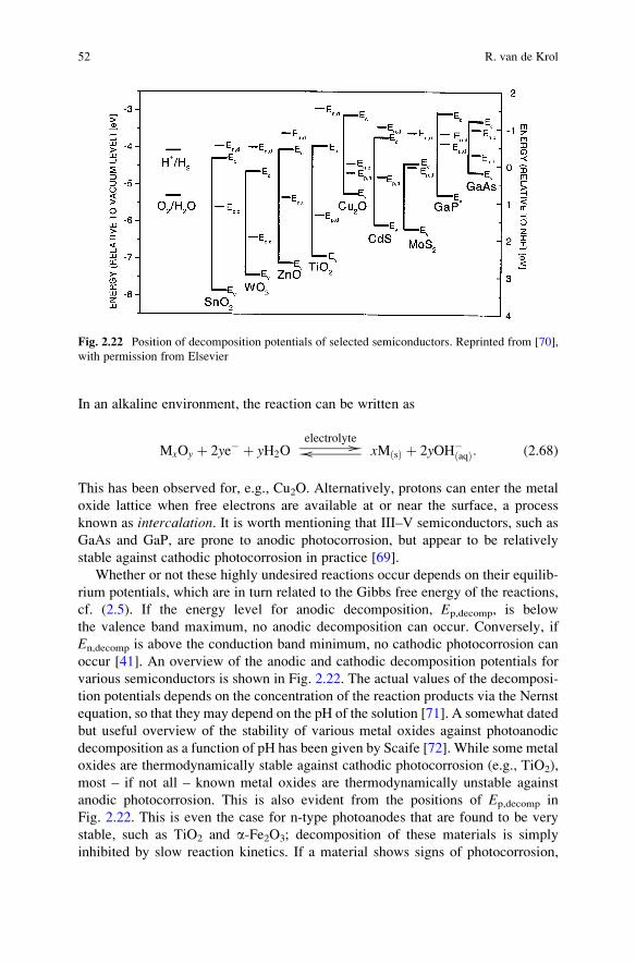
In an alkaline environment, the reaction can be written as
MxOy þ 2ye� þ yH2O! electrolyte
xMðsÞ þ 2yOH�ðaqÞ: (2.68)
This has been observed for, e.g., Cu2O. Alternatively, protons can enter the metal
oxide lattice when free electrons are available at or near the surface, a process
known as intercalation. It is worth mentioning that III–V semiconductors, such as
GaAs and GaP, are prone to anodic photocorrosion, but appear to be relatively
stable against cathodic photocorrosion in practice [69].
Whether or not these highly undesired reactions occur depends on their equilib-
rium potentials, which are in turn related to the Gibbs free energy of the reactions,
cf. (2.5). If the energy level for anodic decomposition, Ep,decomp, is below
the valence band maximum, no anodic decomposition can occur. Conversely, if
En,decomp is above the conduction band minimum, no cathodic photocorrosion can
occur [41]. An overview of the anodic and cathodic decomposition potentials for
various semiconductors is shown in Fig. 2.22. The actual values of the decomposi-
tion potentials depends on the concentration of the reaction products via the Nernst
equation, so that they may depend on the pH of the solution [71]. A somewhat dated
but useful overview of the stability of various metal oxides against photoanodic
decomposition as a function of pH has been given by Scaife [72]. While some metal
oxides are thermodynamically stable against cathodic photocorrosion (e.g., TiO2),
most – if not all – known metal oxides are thermodynamically unstable against
anodic photocorrosion. This is also evident from the positions of Ep,decomp in
Fig. 2.22. This is even the case for n-type photoanodes that are found to be very
stable, such as TiO2 and a-Fe2O3; decomposition of these materials is simply
inhibited by slow reaction kinetics. If a material shows signs of photocorrosion,
Fig. 2.22 Position of decomposition potentials of selected semiconductors. Reprinted from [70],
with permission from Elsevier
52 R. van de Krol

the addition of suitable co-catalysts may alleviate the problem to some extent by
favoring the water oxidation route. In practice, photocorrosion is difficult to predict
and one usually has to put new materials to the test under actual operating
conditions.
2.8 Energy and Quantum Conversion Efficiencies
The energy conversion efficiency is one of the key performance indicators of the
PEC cell. Assuming that all the photogenerated electrons and holes are used for the
water splitting reaction, the overall solar-to-hydrogen efficiency is given by
�STH ¼Poutelectrical � Pin
electrical
Plight
¼ jphoto Vredox � Vbiasð ÞPlight
: (2.69)
Vredox is usually taken to be 1.23 V (at room temperature), based on a Gibbs free
energy change for water splitting of 237 kJ/mol. Alternatively, the enthalpy change
(286 kJ/mol) is sometimes used, which corresponds to a redox potential of 1.48 V.
The latter value is appropriate when the hydrogen produced will be used in a
combustion process, whereas the former value is more appropriate when the
hydrogen is converted into electricity in a fuel cell [69]. When the end-use of the
produced H2 is not clear, it is probably best to use the Gibbs free energy value since
it yields more conservative efficiency numbers. Assuming AM1.5G incident sun-
light (Plight ¼ 1,000 W/m2) and no applied bias, the efficiency can be directly
related to the photocurrent by �STH ¼ 1.23 � jphoto, with the efficiency in % and
the photocurrent in mA/cm2. Hence, a photocurrent of ~8 mA/cm2 is required to
reach the 10% efficiency target for economically viable PEC cells (see Chap. 8).
It should be emphasized that Vbias in (2.69) refers to the actual potential
difference between the working and counter electrodes. Attempts to indirectly
determine this potential difference from the results of a three-electrode measure-
ment (in which the working electrode potential is reported relative to that of
a reference electrode) generally leads to errors, and should be avoided (see also
Chap. 3).
A more direct method to determine the solar-to-hydrogen efficiency is to mea-
sure the amount of evolved hydrogen by mass spectrometry, gas chromatography
[73, 74], or by following the water displacement in an inverted burette. The STH
efficiency for this approach is given by
�STH ¼FH2
G0f;H2
Plight
; (2.70)
where FH2is rate of H2 evolution at the illuminated area (mol/s/m2) and G0
f;H2is the
Gibbs free energy of formation of hydrogen (237 kJ/mol).
2 Principles of Photoelectrochemical Cells 53

When reporting STH efficiencies, care should be taken to ensure that (a) the
water splitting reaction is stoichiometric (H2:O2 ¼ 2:1), (b) no other reactions due
to, e.g., sacrificial donors/acceptors occur, and (c) the light source is well specified
and closely matches the AM1.5G spectrum in intensity and spectral distribution
[75]. For more detailed information on STH efficiency measurements, the reader is
referred to some useful guidelines reported by a US Department of Energy (DOE)
working group on photoelectrochemical hydrogen production [76] and to a careful
study on the influence of the type of light source used [77].
When trying to identify performance-limiting factors in PEC photoelectrodes,
the quantum efficiency as a function of wavelength is a particularly useful parame-
ter. The definition of the external quantum efficiency is the fraction of the incident
photons that is converted to electrons that can be measured by the outer circuit. This
is the IPCE (incident photon-to-current conversion efficiency), which is given by
IPCEðlÞ ¼ hc
e
jphotoðlÞlPðlÞ
� �: (2.71)
IPCE values in excess of 80% for the photo-oxidation of water have been reported
for, e.g., WO3 [78] and for TiO2 under UV illumination [79]. Another useful
parameter is the APCE, or absorbed photon-to-current conversion efficiency. Incontrast to the IPCE, the APCE also corrects for reflection losses. Often referred to
as the internal quantum efficiency, it is related to the IPCE via
APCEðlÞ ¼ IPCEðlÞAðlÞ ¼
IPCEðlÞ1� R� T
(2.72)
A, R, and T are the optical absorption, reflection, and transmission, respectively.
The optical absorption is not to be confused with the absorbance or optical density,which is given by
OD ¼ �Log T
1� R
� �¼ aL
2:303: (2.73)
Here, a is the absorption coefficient and L is the film thickness. The APCE is the
more useful parameter when evaluating recombination within the semiconductor,
while the IPCE is more appropriate to evaluate device-level conversion efficiencies.
Of particular interest is the use of IPCE values measured under monochromatic
irradiation to predict the photocurrent under actual solar irradiation:
Jsolar ¼Z
IPCEðlÞ � FðlÞ � eð Þ dl: (2.74)
Here, Jsolar is the total solar photocurrent in A/m2 and F(l) is the photon flux of
sunlight in photons/m2/s. The photon flux can be calculated from tabulated solar
54 R. van de Krol
irradiance data, E(l), via F(l) ¼ E(l)/(hc/l) [75]. An important underlying
assumption for (2.74) is that there is a linear relationship between the monochro-
matic photocurrent and the light intensity. This is often the case, but there are
exceptions. A super-linear increase of the photocurrent with light intensity is
sometimes observed for nanostructured materials with high concentrations of
relatively shallow surface or interface traps; these traps first need to be filled before
the charge carriers can reach the electrolyte or the back contact [80]. Conversely,
slow charge transport or charge transfer across the interface may lead to an
accumulation of free charge carriers at or near the interface. This increases the
amount of recombination and will result in a sublinear increase of the photocurrent
with light intensity.
2.9 Photoelectrode Requirements and Cell Configurations
The most critical aspect of the design of a photoelectrochemical device for water
splitting is the choice of suitable photoanode and/or photocathode materials. Sev-
eral of the requirements imposed on these materials appear to be in conflict, and
certain trade-offs have to be made. In some cases, these trade-offs can be avoided
by adopting smart architectures and materials combinations. The remainder of this
chapter gives a few general considerations and approaches; more detailed accounts
of strategies to cope with these trade-offs are given in later chapters.
2.9.1 Requirements and Trade-offs
Most of the requirements for suitable water-splitting photoanode and/or photocath-
ode materials have already been alluded to in the previous sections of this chapter.
They can be summarized as follows [81]:
• Good (visible) light absorption
• High chemical stability in the dark and under illumination
• Band edge positions that straddle the water reduction and oxidation potentials
• Efficient charge transport in the semiconductor
• Low overpotentials for reduction/oxidation of water
• Low cost
The spectral region in which the semiconductor absorbs light is determined by
the bandgap of the material. The minimum bandgap is determined by the energy
required to split water (1.23 eV) plus the thermodynamic losses (0.3–0.4 eV [82])
and the overpotentials that are required at various points in the system to ensure
sufficiently fast reaction kinetics (0.4–0.6 eV) [77, 83]. As a result, the bandgap
should be at least 1.9 eV, which corresponds to an absorption onset at 650 nm.
Below 400 nm the intensity of sunlight drops rapidly, imposing an upper limit of
2 Principles of Photoelectrochemical Cells 55

3.1 eV on the bandgap. Hence, the optimum value of the bandgap should be
somewhere between 1.9 and 3.1 eV, which is within the visible range of the solar
spectrum. In a thorough analysis, Murphy et al. suggested an optimum bandgap of
2.03 eV, which would lead to a solar-to-hydrogen efficiency of 16.8% [77].
The chemical stability requirement is a severe one that limits the usefulness
of many photo-active materials. Most nonoxide semiconductors either dissolve or
form a thin oxide layer that prevents charge transfer across the semiconductor/
electrolyte interface. Oxide semiconductors are more stable, but may be prone to
anodic or cathodic decomposition, as outlined in Sect. 2.7.4. The general trend is
that the stability against (photo)corrosion increases with increasing bandgap.
Although this conflicts with the requirement of visible light absorption, a small
bandgap and good chemical stability are not necessarily mutually exclusive
(although one could argue that a small bandgap is often accompanied by a high
valence band energy, which would indeed result in a less stable material).
Few semiconductors fulfill the third requirement, which states that the band
edges should straddle the water reduction and oxidation potentials. As shown in
Fig. 2.18, the ones that do either have a bandgap that is too large (e.g., SrTiO3, SiC)
or are unstable in aqueous solutions (Cu2O, CdS). This figure also suggests that the
band edges of nonoxide semiconductors tend to be better suited toward the reduc-
tion of water (high EC), whereas those of oxide semiconductors favor water oxida-
tion (low EV). It should be mentioned that the third requirement is actually a bit
more stringent than Fig. 2.18 suggests. As pointed out originally by Gerischer [84],
and reiterated later by Weber [85], it is the quasi-Fermi levels that should straddle
the water redox potentials. Although the interpretation of the quasi-Fermi level as a
thermodynamic driving force may not be entirely appropriate under all conditions
(cf. Sect. 2.7.1), using it within the context of the third requirement seems
reasonable.
The fourth requirement, that of efficient charge transport, is easily fulfilled in
some materials (TiO2, WO3), while in others it is one of the main causes of poor
overall conversion efficiencies. A particularly important example of the latter is that
of a-Fe2O3, which will be discussed in detail in Chap. 4. One can distinguish
intrinsic and extrinsic charge transport factors. As outlined in Sect. 2.2, the elec-
tronic band structure of the material gives important clues with regard to the
intrinsic charge carrier mobilities. Extensive overlap of metal 3d orbitals usually
leads to high electron mobilities, whereas the overlap of O-2p orbitals determines
the hole mobility in most metal oxides. Extrinsic factors, in particular shallow
donors/acceptors and recombination centers, are perhaps even more important. For
example, electron transport was found to be rate limiting in spray-deposited,
undoped films of a-Fe2O3, whereas hole transport was found to be rate limiting
after donor doping the material with silicon [86]. The susceptibility to recombina-
tion is often expressed as the carrier lifetime, tR, or the minority carrier diffusion
length, LD. They are related through
LD ’ffiffiffiffiffiffiffiffiffiDtRp
: (2.75)
56 R. van de Krol

The diffusivity of the free carriers, D, is related to their mobility, m, via the
Nernst–Einstein equation:
D ¼ kTme
: (2.76)
Values of LD range from several nanometers in some oxides to several hundred
micrometers in high-purity silicon.
For n-type semiconductors, the fifth requirement implies that hole transfer across
the semiconductor/electrolyte interface should be sufficiently fast in order to
compete with the anodic decomposition reaction. More generally, interfacial charge
transfer should be fast enough to avoid the accumulation carriers at the surface, as
this would lead to a decrease of the electric field and a concomitant increase in
electron–hole recombination. To improve the kinetics of charge transfer, catalyti-
cally active surface species can be added. Examples of effective oxygen evolution
catalysts are RuO2 [87], IrOx [88], and Co-based compounds [64], whereas Pt, Rh
[89], Cr–Rh, RuO2, or NiOx [73, 90] are usually employed as a catalysts for
hydrogen evolution.
At this time, no single material has been found that meets all these requirements.
Four main trade-offs can be identified:
• Bandgap$ stability
• Photon collection$ charge transport
• Recombination$ catalysis
• Performance$ cost
The bandgap vs. stability issue has been discussed above. The second trade-off is
especially important for semiconductors with a small absorption coefficient, such as
metal oxides with an indirect bandgap. In these materials most of the electron–hole
pairs are generated far away from the surface, and the carriers recombine before
reaching the interface (cf. Fig. 2.23). The third trade-off reflects the tendency of
catalytically active surface sites to also act as efficient recombination centers for
electronic charge carriers. Moreover, certain co-catalysts for hydrogen or oxygen
evolution may also enhance the back-reaction between H2 and O2. A well-known
example is Pt. This may be a problem for cell designs in which the cross-over of
gases generated at the (photo)anode and (photo)cathode cannot be avoided. Inter-
estingly, NiO is an efficient hydrogen evolution catalyst at which the H2 + O2 back-
reaction does not seem to occur [73]. The final trade-off reflects the main reason for
the interest in low-cost metal oxides, since the economic viability of state-of-the-art
multijunction devices based on, e.g., high quality III–V materials grown by MO-
CVD or MBE is doubtful [91].
2 Principles of Photoelectrochemical Cells 57

2.9.2 Nanostructured Electrodes
Nanostructured electrode morphologies can be used to address some of the intrinsic
material’s limitations and trade-offs mentioned above. The most obvious advantage
of a nanostructured morphology is the increase in specific surface area. The
concomitant increase in the number of surface sites greatly enhances the overall
charge transfer kinetics at the semiconductor/electrolyte interface.
A second advantage is the shorter diffusion path lengths for the photogenerated
charge carriers. This is illustrated by the nanowire array photoelectrode shown
in Fig. 2.24 (left), where the minority carriers only have to travel half the diameter
of the nanowire in order to reach the semiconductor/electrolyte interface [92].
If transport of majority carriers is also an issue, one could employ an array of a
conducting wires, which are coated with a thin film of the photoactive semiconduc-
tor (Fig. 2.24, right). Here, both minority and majority carriers benefit from the
short distance (�d) that they have to travel before reaching the electrolyte and
conducting core, respectively. This is sometimes referred to as a “guest–host”
structure, in which the light absorbing nanosized guest material is attached to a
nanostructured host scaffold [93]. The advantages are not limited to the highly
regular nanowire array architecture shown in Fig. 2.24; nanostructures based on
dendritic or cauliflower-type morphologies or randomly packed spheres offer
similar advantages [78, 93, 94]. Such structures are discussed in more detail in
Chaps. 4 and 9.
Fig. 2.23 Absorption regions in a semiconducting photoanode. The intensity of the light (F)decreases exponentially with distance from the surface (Lambert-Beer law). All charge carriers
generated within a distance LD + W from the surface contribute to the photocurrent (regions I and
II), whereas all carriers generated in region III recombine
58 R. van de Krol
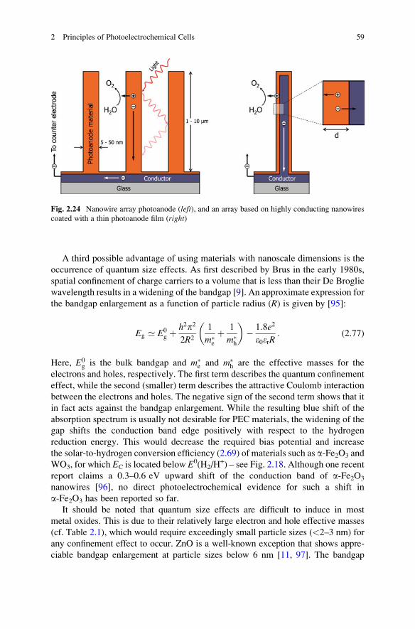
A third possible advantage of using materials with nanoscale dimensions is the
occurrence of quantum size effects. As first described by Brus in the early 1980s,
spatial confinement of charge carriers to a volume that is less than their De Broglie
wavelength results in a widening of the bandgap [9]. An approximate expression for
the bandgap enlargement as a function of particle radius (R) is given by [95]:
Eg ’ E0g þ
h2p2
2R2
1
m�eþ 1
m�h
� �� 1:8e2
e0erR: (2.77)
Here, E0g is the bulk bandgap and m�e and m�h are the effective masses for the
electrons and holes, respectively. The first term describes the quantum confinement
effect, while the second (smaller) term describes the attractive Coulomb interaction
between the electrons and holes. The negative sign of the second term shows that it
in fact acts against the bandgap enlargement. While the resulting blue shift of the
absorption spectrum is usually not desirable for PEC materials, the widening of the
gap shifts the conduction band edge positively with respect to the hydrogen
reduction energy. This would decrease the required bias potential and increase
the solar-to-hydrogen conversion efficiency (2.69) of materials such as a-Fe2O3 and
WO3, for which EC is located below E0(H2/H+) – see Fig. 2.18. Although one recent
report claims a 0.3–0.6 eV upward shift of the conduction band of a-Fe2O3
nanowires [96], no direct photoelectrochemical evidence for such a shift in
a-Fe2O3 has been reported so far.
It should be noted that quantum size effects are difficult to induce in most
metal oxides. This is due to their relatively large electron and hole effective masses
(cf. Table 2.1), which would require exceedingly small particle sizes (<2–3 nm) for
any confinement effect to occur. ZnO is a well-known exception that shows appre-
ciable bandgap enlargement at particle sizes below 6 nm [11, 97]. The bandgap
Fig. 2.24 Nanowire array photoanode (left), and an array based on highly conducting nanowires
coated with a thin photoanode film (right)
2 Principles of Photoelectrochemical Cells 59

enlargement is generally asymmetric, with DEC ¼ h2p2=ð2R2m�eÞ and DEV ¼ h2p2=ð2R2m�hÞ. This asymmetry is less evident in ZnO ðm�e ¼ 0:24me; m
�h ¼ 0:24meÞ than
in anatase TiO2 ðm�h ¼ 0:8me; m�e ¼ 10meÞ, for which any bandgap enlargement
appears to be solely due to a shift in EV [11]. Clearly, if quantum confinement is to be
used to shift the conduction band edge to higher energies without increasing the
bandgap too much, one would prefer to have a semiconductor with a small electron
effective mass and a large hole effective mass.
An important aspect of nanosized semiconductors is the absence of band
bending. Since the number of ionized donors or acceptors in nanosized particles
is very small, such particles cannot sustain a large built-in electric field (cf. (2.41)
and Fig. 2.13, left). The maximum attainable potential drop within a spherical
semiconductor particle with radius R and a donor (or acceptor) density ND is
given by [98]:
fSC ¼�eNDR
2
6e0er: (2.78)
From this expression, the band bending in a 10 nm a-Fe2O3 particle (R ¼ 5 nm,
er ¼ 25) with a relatively high donor density of 1018 cm�3 is limited to ~3 mV. This
clearly shows that the electric field in the space charge of a nanoparticle cannot
play a significant role in the separation of photogenerated electrons and holes.
Fortunately, most carriers are nevertheless able to reach the interface since the
minority carrier diffusion length is – with few exceptions – much larger than the
radius of the nanoparticle. As a result, the charge transfer kinetics at the semicon-
ductor/electrolyte interface usually dominate the overall charge separation and
recombination kinetics in nanoparticles.
2.9.3 PEC Device Configurations
When the conduction and valence bands do not straddle the water reduction and
oxidation potentials, or if the available overpotentials for water splitting are insuf-
ficient, a combination of two or more semiconductors may offer a solution. In such
a device, one semiconductor acts as a regular photoanode or photocathode. The
other semiconductor(s) function(s) as either a complementary photoelectrode, or as
an integrated photovoltaic device that provides a bias voltage. Figure 2.25 shows
some examples of possible configurations.
Configuration (A) is the one we have used throughout this chapter to illustrate the
main principles of photoelectrochemical water splitting. Strontium titanate, SrTiO3,
is one of very few materials that have been observed to split water in this configura-
tion [99]. However, the efficiency is less than 1% due to its large bandgap (3.2 eV).
Cuprous oxide, Cu2O, and p-type SiC are candidates for configuration (B). While
Cu2O has been found to suffer from photoreduction to metallic Cu [100, 101],
60 R. van de Krol

other reports indicate that it may be stable under the right conditions [68, 102].
The 4H polytype of silicon carbide is one of the few chemically stable photocathode
materials able to split water, but its efficiency is also low (Eg ¼ 3.26 eV) [67].
In configurations (C) and (D) a bias voltage is applied to the photoanode and
photocathode, respectively, through an integrated p–n junction. Turner et al. have
Fig. 2.25 Examples of possible PEC configurations under illumination. Top row: Standard single-semiconductor devices based on a photoanode (a) or photocathode (b) with a metal counter
electrode. Middle row: Monolithic devices based on a photoanode (c) or photocathode (d) biased
with an integrated p–n junction. Bottom row: p–n junction photoelectrochemical device (e), and an
n–n heterojunction PEC device based on a photoanode deposited on top of a second n-type
semiconductor that “boosts” the energy of the electrons (f)
2 Principles of Photoelectrochemical Cells 61

demonstrated such a monolithic tandem device based on a photocathode of p-type
GaInP2 in combination with a GaAs p–n junction [103]. They achieved an
impressive solar-to-hydrogen efficiency of 12.4%, but the rapid degradation and
high cost of the device limit its practical use. Gr€atzel and Augustynski used a
dye-sensitized solar cell (DSSC) to bias a WO3 or Fe2O3 photoanode [91, 104]. The
photoanode absorbs the blue part of the solar spectrum (Eg ¼ 2.6 eV for WO3),
whereas the DSSC absorbs red light. This approach is somewhat similar to config-
uration (C), except for the fact that the p–n junction is replaced by a separate DSSC
device. The advantage is that the entire system can be made from low-cost and
stable metal oxides. A remaining challenge is to address the significant light
scattering of the individual (nanostructured) components, which severely limits
the efficiency of the total system [105].
In configurations (E) and (F) an additional bias potential is generated by a single
additional absorber instead of a p–n junction. An example of configuration (E) is a
device based on n-type TiO2 (Eg ¼ 3.2 eV) and p-type GaP (Eg ¼ 2.25 eV) [106].
The difference in bandgaps ensures that a large part of the solar spectrum is used.
This is not the case for p–n homojunctions, and devices such as n-Fe2O3/p-Fe2O3
[107] will not be very efficient because of this. The n–n heterojunction of configu-
ration (F) was first studied many years ago, and was not considered to be very useful
since the photogenerated holes in the buried n-type semiconductor could not reach
the photoanode/electrolyte interface [108]. More recently, however, Yang et al.
showed that n-type Si underneath n-type TiO2 “boosts” the energy of TiO2 conduc-
tion band electrons [50]. This increases the available overpotential for the reduction
of water and improves the kinetics.
Acknowledgments The author gratefully acknowledges Fatwa F. Abdi for critical reading of the
manuscript, and the NWO-ACTS Sustainable Hydrogen program (project 053.61.009) and the
European Commission’s Framework 7 program (NanoPEC, Project 227179) for support.
References
1. Chelikowsky, J.R., Cohen, M.L.: Electronic-structure of silicon. Phys. Rev. B 10, 5095–5107
(1974)
2. Fujishima, A., Honda, K.: Electrochemical photolysis of water at a semiconductor electrode.
Nature 238, 37–38 (1972)
3. Osterloh, F.E.: Inorganic materials as catalysts for photochemical splitting of water. Chem.
Mater. 20, 35–54 (2008)
4. Stoyanov, E., Langenhorst, F., Steinle-Neumann, G.: The effect of valence state and site
geometry on Ti L-3, L-2 and O-K electron energy-loss spectra of TixOy phases. Am. Miner.
92, 577–586 (2007)
5. Fischer, D.W.: X-ray band spectra and molecular-orbital structure of rutile TiO2. Phys. Rev.
B 5, 4219 (1972)
6. Hoffmann, R.: Solids and Surfaces – A Chemist’s View of Bonding in Extended Structures.
Wiley-VCH, Weinheim (1988)
62 R. van de Krol

7. Tauc, J., Grigorov, R., Vancu, A.: Optical properties and electronic structure of amorphous
germanium. Phys. Stat. Sol. 15, 627 (1966)
8. Sze, S.M.: Physics of Semiconductor Devices. Wiley, New York (1981)
9. Brus, L.E.: Electron electron and electron–hole interactions in small semiconductor
crystallites – the size dependence of the lowest excited electronic state. J. Chem. Phys. 80,
4403–4409 (1984)
10. Deskins, N.A., Dupuis, M.: Intrinsic hole migration rates in TiO2 from density functional
theory. J. Phys. Chem. C 113, 346–358 (2009)
11. Enright, B., Fitzmaurice, D.: Spectroscopic determination of electron and hole effective
masses in a nanocrystalline semiconductor film. J. Phys. Chem. 100, 1027–1035 (1996)
12. Berak, J.M., Sienko, M.J.: Effect of oxygen-deficiency on electrical transport properties of
tungsten trioxide crystals. J. Solid State Chem. 2, 109–133 (1970)
13. Bosman, A.J., Vandaal, H.J.: Small-polaron versus band conduction in some transition-metal
oxides. Adv. Phys. 19, 1 (1970)
14. Matsuzaki, K., Nomura, K., Yanagi, H., Kamiya, T., Hirano, M., Hosono, H.: Epitaxial
growth of high mobility Cu2O thin films and application to p-channel thin film transistor.
Appl. Phys. Lett. 93, 202107 (2008)
15. Kawazoe, H., Yasukawa, M., Hyodo, H., Kurita, M., Yanagi, H., Hosono, H.: P-type
electrical conduction in transparent thin films of CuAlO2. Nature 389, 939–942 (1997)
16. Kudo, A., Yanagi, H., Hosono, H., Kawazoe, H.: SrCu2O2: a p-type conductive oxide with
wide band gap. Appl. Phys. Lett. 73, 220–222 (1998)
17. Bessekhouad, Y., Gabes, Y., Bouguelia, A., Trari, M.: The physical and photo electrochemi-
cal characterization of the crednerite CuMnO2. J. Mater. Sci. 42, 6469–6476 (2007)
18. Pierret, R.F.: Advanced semiconductor fundamentals. Addison-Wesley, Reading (1989)
19. Asahi, R., Morikawa, T., Ohwaki, T., Aoki, K., Taga, Y.: Photocatalysts sensitive to visible
light – response. Science 295, 627–627 (2002)
20. Maruska, H.P., Ghosh, A.K.: Transition-metal dopants for extending the response of titanate
photoelectrolysis anodes. Solar Energy Mater. 1, 237–247 (1979)
21. Salvador, P.: Analysis of the physical properties of TiO2-Be electrodes in the photoassisted
oxidation of water. Solar Energy Mater. 6, 241–250 (1982)
22. Henrich, V.E., Cox, P.A.: The surface science of metal oxides. Cambridge University Press,
Cambridge (1994)
23. Kato, H., Kudo, A.: Visible-light-response and photocatalytic activities of TiO2 and SrTiO3
photocatalysts codoped with antimony and chromium. J. Phys. Chem. B 106, 5029–5034
(2002)
24. Howe, A.T., Hawkins II, R.T., Fleisch, T.H.: Photoelectrochemical cells of the electrolyte–
metal–insulator–semiconductor (EMIS) configuration. I. Metal thickness and coverage
effects in the Pt/silicon oxide/n-Si system. J. Electrochem. Soc. 133, 1369–1375 (1986)
25. Piazza, F., Pavesi, L., Henini, M., Johnston, D.: Effect of as overpressure on Si-doped (111)
a gaas grown by molecular-beam epitaxy – a photoluminescence study. Semicond. Sci.
Technol. 7, 1504–1507 (1992)
26. Kr€oger, F.A.: The chemistry of imperfect crystals. North-Holland Publishing Co.,
Amsterdam (1964)
27. Chiang, Y.-M., Birnie III, D., Kingery, D.W.: Physical Ceramics. Wiley, New York (1997)
28. Smyth, D.M.: The Defect Chemistry of Metal Oxides. Oxford University Press, New York
(2000)
29. Jorand Sartoretti, C., Alexander, B.D., Solarska, R., Rutkowska, W.A., Augustynski, J.,
Cerny, R.: Photoelectrochemical oxidation of water at transparent ferric oxide film
electrodes. J. Phys. Chem. B 109, 13685–13692 (2005)
30. Liang, Y., Enache, C.S., Van de Krol, R.: Photoelectrochemical characterization of sprayed
a-Fe2O3 thin films: Influence of Si-doping and SnO2 interfacial layer. Int. J. Photoenergy
(2008). doi:10.1155/2008/739864
2 Principles of Photoelectrochemical Cells 63

31. Kennedy, J.H., Shinar, R., Ziegler, J.P.: Alpha-Fe2O3 photoanodes doped with silicon.
J. Electrochem. Soc. 127, 2307–2309 (1980)
32. Liang, Y., Tsubota, T., Mooij, L.P.A., van de Krol, R.: Highly improved quantum efficiencies
for thin film BiVO4 photoanodes. J. Phys. Chem. C 115, 17594–17598 (2011)
33. Das Mulmi, D., Sekiya, T., Kamiya, N., Kurita, S., Murakami, Y., Kodaira, T.: Optical and
electric properties of Nb-doped anatase TiO2 single crystal. J. Phys. Chem. Solids 65,
1181–1185 (2004)
34. Anpo, M., Takeuchi, M.: The design and development of highly reactive titanium oxide
photocatalysts operating under visible light irradiation. J. Catal. 216, 505–516 (2003)
35. Kudo, A., Ueda, K., Kato, H., Mikami, I.: Photocatalytic O2 evolution under visible light
irradiation on BiVO4 in aqueous AgNO3 solution. Catal. Lett. 53, 229–230 (1998)
36. Sayama, K., Nomura, A., Arai, T., Sugita, T., Abe, R., Yanagida, M., Oi, T., Iwasaki, Y., Abe,
Y., Sugihara, H.: Photoelectrochemical decomposition of water into H2 and O2 on porous
BiVO4 thin-film electrodes under visible light and significant effect of Ag ion treatment.
J. Phys. Chem. B 110, 11352–11360 (2006)
37. Pierret, R.F.: Semiconductor Device Fundamentals. Addison Wesley, Reading (1996)
38. Nicollian, E.H., Brews, J.R.: MOS (metal oxide semiconductor) Physics and Technology.
Wiley, Hoboken (2003)
39. Onari, S., Arai, T., Kudo, K.: Ir lattice-vibrations and dielectric-dispersion in alpha-Fe2O3.
Phys. Rev. B 16, 1717–1721 (1977)
40. Rosso, K.M., Smith, D.M.A., Dupuis, M.: An ab initio model of electron transport in hematite
(alpha-Fe2O3) basal planes. J. Chem. Phys. 118, 6455–6466 (2003)
41. Morrison, S.R.: Electrochemistry of semiconductor and oxidized metal electrodes. Plenum,
New York (1980)
42. Bockris, J.O.M., Reddy, A.K.N., Galboa-Aldeco, M.E.: Modern Electrochemistry 2A –
Fundamentals of Electrodics. Springer, New York (2001)
43. Memming, R.: Semiconductor Electrochemistry. Wiley, New York (2000)
44. McNaught, A.D., Wilkinson, A.: IUPAC Compendium of Chemical Terminology, 2nd edn.
(the “Gold Book”). Blackwell Scientific Publications, Oxford (1997). http://goldbook.iupac.
org/S05917.html. Accessed 8 Sep 2010
45. Reichman, J.: The current–voltage characteristics of semiconductor-electrolyte junction
photo-voltaic cells. Appl. Phys. Lett. 36, 574–577 (1980)
46. Peter, L.M., Li, J., Peat, R.: Surface recombination at semiconductor electrodes. 1. Transient
and steady-state photocurrents. J. Electroanal. Chem. 165, 29–40 (1984)
47. Gandia, J., Pujadas, M., Salvador, P.: Electrolyte electroreflectance – easy and reliable flat-
band potential measurements. J. Electroanal. Chem. 244, 69–79 (1988)
48. Radecka, M., Sobas, P., Wimbicka, M., Rekas, M.: Photoelectrochemical properties of
undoped and Ti-doped WO3. Phys. B Condens. Matter 364, 85–92 (2005)
49. Hagfeldt, A., Bj€orksten, U., Gr€atzel, M.: Photocapacitance of nanocrystalline oxide semicon-
ductor films: band-edge movement in mesoporous TiO2 electrodes during UV illumination. J.
Phys. Chem. 100, 8045–8048 (1996)
50. Hwang, Y.J., Boukai, A., Yang, P.D.: High density n-Si/n-TiO2 core/shell nanowire arrays
with enhanced photoactivity. Nano Lett. 9, 410–415 (2009)
51. Marcus, R.A.: Theory of oxidation–reduction reactions involving electron transfer 1.
J. Chem. Phys. 24, 966–978 (1956)
52. Marcus, R.A.: Chemical + electrochemical electron-transfer theory. Ann. Rev. Phys. Chem.
15, 155 (1964)
53. Gerischer, H.: Charge transfer processes at semiconductor-electrolyte interfaces in connec-
tion with problems of catalysis. Surf. Sci. 18, 97 (1969)
54. Duret, A., Gr€atzel, M.: Visible light-induced water oxidation on mesoscopic alpha-Fe2O3
films made by ultrasonic spray pyrolysis. J. Phys. Chem. B 109, 17184–17191 (2005)
55. Jarrett, H.S.: Photocurrent conversion efficiency in a Schottky-barrier. J. Appl. Phys. 52,
4681–4689 (1981)
64 R. van de Krol

56. Wilson, R.H.: Model for current–voltage curve of photoexcited semiconductor electrodes.
J. Appl. Phys. 48, 4292–4297 (1977)
57. Salvador, P.: Kinetic approach to the photocurrent transients in water photoelectrolysis
at n-TiO2 electrodes. I. Analysis of the ratio of the instantaneous to steady-state photocurrent.
J. Phys. Chem. 89, 3863–3869 (1985)
58. Kisumi, T., Tsujiko, A., Murakoshi, K., Nakato, Y.: Crystal-face and illumination intensity
dependences of the quantum efficiency of photoelectrochemical etching, in relation to those
of water photooxidation, at n-TiO2 (rutile) semiconductor electrodes. J. Electroanal. Chem.
545, 99–107 (2003)
59. Imanishi, A., Okamura, T., Ohashi, N., Nakamura, R., Nakato, Y.: Mechanism of water
photooxidation reaction at atomically flat TiO2 (rutile) (110) and (100) surfaces: dependence
on solution pH. J. Am. Chem. Soc. 129, 11569–11578 (2007)
60. Rossmeisl, J., Qu, Z.W., Zhu, H., Kroes, G.J., Norskov, J.K.: Electrolysis of water on oxide
surfaces. J. Electroanal. Chem. 607, 83–89 (2007)
61. Valdes, A., Qu, Z.W., Kroes, G.J., Rossmeisl, J., Norskov, J.K.: Oxidation and photo-
oxidation of water on TiO2 surface. J. Phys. Chem. C 112, 9872–9879 (2008)
62. Valdes, A., Kroes, G.J.: First principles study of the photo-oxidation of water on tungsten
trioxide (WO3). J. Chem. Phys. 130(11), 114701 (2009)
63. Harriman, A., Pickering, I.J., Thomas, J.M., Christensen, P.A.: Metal-oxides as heteroge-
neous catalysts for oxygen evolution under photochemical conditions. J. Chem. Soc. Faraday
Trans. I 84, 2795–2806 (1988)
64. Kanan, M.W., Nocera, D.G.: In situ formation of an oxygen-evolving catalyst in neutral water
containing phosphate and Co2+. Science 321, 1072–1075 (2008)
65. Jiao, F., Frei, H.: Nanostructured cobalt oxide clusters in mesoporous silica as efficient
oxygen-evolving catalysts. Angew. Chem. Int. Ed. 48, 1841–1844 (2009)
66. Kay, A., Cesar, I., Gr€atzel, M.: New benchmark for water photooxidation by nanostructured
alpha-Fe2O3 films. J. Am. Chem. Soc. 128, 15714–15721 (2006)
67. Van Dorp, D.H., Hijnen, N., Di Vece, M., Kelly, J.J.: SiC: a photocathode for water splitting
and hydrogen storage. Angew. Chem. Int. Ed. 48, 6085–6088 (2009)
68. De Jongh, P.E., Vanmaekelbergh, D., Kelly, J.J.: Photoelectrochemistry of electrodeposited
Cu2O. J. Electrochem. Soc. 147, 486–489 (2000)
69. Rajeshwar, K., McConnell, R., Licht, S.: Solar hydrogen generation – toward a renewable
energy future. Springer, New York (2008)
70. Bak, T., Nowotny, J., Rekas, M., Sorrell, C.C.: Photo-electrochemical hydrogen generation
from water using solar energy. Materials-related aspects. Int. J. Hydrogen Energy 27,
991–1022 (2002)
71. Park, S.M., Barber, M.E.: Thermodynamic stabilities of semiconductor electrodes.
J. Electroanal. Chem. 99, 67–75 (1979)
72. Scaife, D.E.: Oxide semiconductors in photoelectrochemical conversion of solar energy.
Solar Energy 25, 41–54 (1980)
73. Kudo, A., Miseki, Y.: Heterogeneous photocatalyst materials for water splitting. Chem. Soc.
Rev. 38, 253–278 (2009)
74. Ritterskamp, P., Kuklya, A., Wustkamp, M.A., Kerpen, K., Weidenthaler, C., Demuth, M.:
A titanium disilicide derived semiconducting catalyst for water splitting under solar radiation –
reversible storage of oxygen and hydrogen. Angew. Chem. Int. Ed. 46, 7770–7774 (2007)
75. Solar Irradiance Data, ASTM-G173-03 (AM1.5, global tilt): http://rredc.nrel.gov/solar/
spectra/am1.5/. Accessed 11 Aug 2010
76. Chen, Z.B., Jaramillo, T.F., Deutsch, T.G., Kleiman-Shwarsctein, A., Forman, A.J., Gaillard,
N., Garland, R., Takanabe, K., Heske, C., Sunkara, M., McFarland, E.W., Domen, K., Miller,
E.L., Turner, J.A., Dinh, H.N.: Accelerating materials development for photoelectrochemical
hydrogen production: standards for methods, definitions, and reporting protocols. J. Mater.
Res. 25, 3–16 (2010)
2 Principles of Photoelectrochemical Cells 65

77. Murphy, A.B., Barnes, P.R.F., Randeniya, L.K., Plumb, I.C., Grey, I.E., Horne, M.D.,
Glasscock, J.A.: Efficiency of solar water splitting using semiconductor electrodes. Int.
J. Hydrogen Energy 31, 1999–2017 (2006)
78. Santato, C., Ulmann, M., Augustynski, J.: Enhanced visible light conversion efficiency using
nanocrystalline WO3 films. Adv. Mater. 13, 511 (2001)
79. Kavan, L., Gr€atzel, M.: Highly efficient semiconducting TiO2 photoelectrodes prepared by
aerosol pyrolysis. Electrochim. Acta 40, 643–652 (1995)
80. De Jongh, P.E., Vanmaekelbergh, D.: Trap-limited electronic transport in assemblies of
nanometer-size TiO2 particles. Phys. Rev. Lett. 77, 3427–3430 (1996)
81. Van de Krol, R., Liang, Y.Q., Schoonman, J.: Solar hydrogen production with nanostructured
metal oxides. J. Mater. Chem. 18, 2311–2320 (2008)
82. Weber, M.F., Dignam, M.J.: Splitting water with semiconducting photoelectrodes efficiency
considerations. Int. J. Hydrogen Energy 11, 225–232 (1986)
83. Bolton, J.R., Strickler, S.J., Connolly, J.S.: Limiting and realizable efficiencies of solar
photolysis of water. Nature 316, 495–500 (1985)
84. Gerischer, H.: Electrochemical behavior of semiconductors under illumination.
J. Electrochem. Soc. 113, 1174 (1966)
85. Weber, M.F., Dignam, M.J.: Efficiency of splitting water with semiconducting
photoelectrodes. J. Electrochem. Soc. 131, 1258–1265 (1984)
86. Liang, Y., Enache, C.S., Van de Krol, R.: Photoelectrochemical characterization of sprayed
a-Fe2O3 thin films: Influence of Si-doping and SnO2 interfacial layer. Int. J. Photoenergy
(2008). doi:10.1155/2008/739864
87. Licht, S., Wang, B., Mukerji, S., Soga, T., Umeno, M., Tributsch, H.: Efficient solar water
splitting, exemplified by RuO2-catalyzed AlGaAs/Si photoelectrolysis. J. Phys. Chem. B 104,
8920–8924 (2000)
88. Youngblood, W.J., Lee, S.H.A., Kobayashi, Y., Hernandez-Pagan, E.A., Hoertz, P.G.,
Moore, T.A., Moore, A.L., Gust, D., Mallouk, T.E.: Photoassisted overall water splitting in
a visible light-absorbing dye-sensitized photoelectrochemical cell. J. Am. Chem. Soc. 131,
926 (2009)
89. Maeda, K., Teramura, K., Lu, D.L., Takata, T., Saito, N., Inoue, Y., Domen, K.: Photocatalyst
releasing hydrogen from water – enhancing catalytic performance holds promise for hydro-
gen production by water splitting in sunlight. Nature 440, 295–295 (2006)
90. Kato, H., Asakura, K., Kudo, A.: Highly efficient water splitting into H2 and O2 over
lanthanum-doped NaTaO3 photocatalysts with high crystallinity and surface nanostructure.
J. Am. Chem. Soc. 125, 3082–3089 (2003)
91. Gr€atzel, M.: Photoelectrochemical cells. Nature 414, 338–344 (2001)
92. Mor, G.K., Prakasam, H.E., Varghese, O.K., Shankar, K., Grimes, C.A.: Vertically oriented
Ti-Fe-O nanotube array films: toward a useful material architecture for solar spectrum water
photoelectrolysis. Nano Lett. 7, 2356–2364 (2007)
93. Sivula, K., Le Formal, F., Gr€atzel, M.: WO3–Fe2O3 photoanodes for water splitting: a host
scaffold guest absorber approach. Chem. Mater. 21, 2862–2867 (2009)
94. Cesar, I., Kay, A., Martinez, J.A.G., Gr€atzel, M.: Translucent thin film Fe2O3 photoanodes for
efficient water splitting by sunlight: nanostructure-directing effect of Si-doping. J. Am.
Chem. Soc. 128, 4582–4583 (2006)
95. Brus, L.: Electronic wave-functions in semiconductor clusters – experiment and theory.
J. Phys. Chem. 90, 2555–2560 (1986)
96. Vayssieres, L., Sathe, C., Butorin, S.M., Shuh, D.K., Nordgren, J., Guo, J.H.: One-dimen-
sional quantum-confinement effect in alpha-Fe2O3 ultrafine nanorod arrays. Adv. Mater. 17,
2320 (2005)
97. Lin, K.F., Cheng, H.M., Hsu, H.C., Lin, L.J., Hsieh, W.F.: Band gap variation of size-
controlled ZnO quantum dots synthesized by sol-gel method. Chem. Phys. Lett. 409,
208–211 (2005)
66 R. van de Krol

98. Goossens, A.: Potential distribution in semiconductor particles. J. Electrochem. Soc. 143,
L131–L133 (1996)
99. Mavroides, J.G., Kafalas, J.A., Kolesar, D.F.: Photoelectrolysis of water in cells with SrTiO3
anodes. Appl. Phys. Lett. 28, 241–243 (1976)
100. Schoppel, H.R., Gerischer, H.: Cathodic reduction of Cu-I oxide electrodes as example for
reduction mechanism of semiconductor crystal. Ber. Bunsenges. Phys. Chem. 75, 1237
(1971)
101. Nagasubramanian, G., Gioda, A.S., Bard, A.J.: Semiconductor electrodes. 37. Photoelectro-
chemical behavior of p-type Cu2O in acetonitrile solutions. J. Electrochem. Soc. 128,
2158–2164 (1981)
102. Hara, M., Kondo, T., Komoda, M., Ikeda, S., Shinohara, K., Tanaka, A., Kondo, J.N., Domen,
K.: Cu2O as a photocatalyst for overall water splitting under visible light irradiation. Chem.
Commun. 3, 357–358 (1998)
103. Khaselev, O., Turner, J.A.: A monolithic photovoltaic-photoelectrochemical device for
hydrogen production via water splitting. Science 280, 425–427 (1998)
104. Gr€atzel, M.: Mesoscopic solar cells for electricity and hydrogen production from sunlight.
Chem. Lett. 34, 8–13 (2005)
105. Brillet, J., Cornuz, M., Le Formal, F., Yum, J.H., Gr€atzel, M., Sivula, K.: Examining
architectures of photoanode-photovoltaic tandem cells for solar water splitting. J. Mater.
Res. 25, 17–24 (2010)
106. Nozik, A.J.: p–n photoelectrolysis cells. Appl. Phys. Lett. 29, 150–153 (1976)
107. Turner, J.E., Hendewerk, M., Somorjai, G.A.: The photodissociation of water by doped iron-
oxides – the unbiased P/N assembly. Chem. Phys. Lett. 105, 581–585 (1984)
108. Kohl, P.A., Frank, S.N., Bard, A.J.: Semiconductor electrodes. 11. Behavior of n-type and
p-type single-crystal semiconductors covered with thin normal-TiO2 films. J. Electrochem.
Soc. 124, 225–229 (1977)
2 Principles of Photoelectrochemical Cells 67

http://www.springer.com/978-1-4614-1379-0