presented by anas mazady, cameron fulton, nicholas williams university of connecticut department of...
TRANSCRIPT

Presented by Anas Mazady, Cameron Fulton, Nicholas Williams
University of Connecticut
Department of Electrical and Computer Engineering
Thursday, April 28, 2011
Optimization of geometric properties concerning phase-change memory
(PCM) mushroom cells
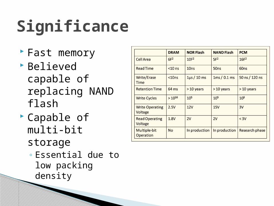
Fast memory Believed capable
of replacing NAND flash
Capable of multi-bit storage Essential due to low
packing density
Significance
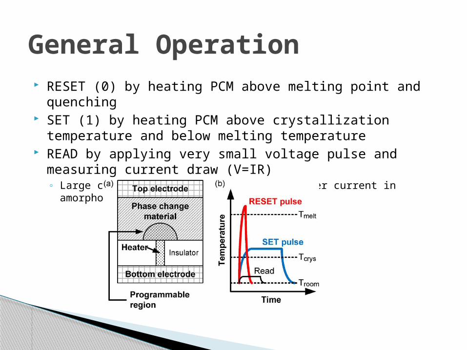
RESET (0) by heating PCM above melting point and quenching
SET (1) by heating PCM above crystallization temperature and below melting temperature
READ by applying very small voltage pulse and measuring current draw (V=IR) Large current in crystalline phase, smaller current in amorphous phase
General Operation

OXIDETiN
GST
TiN
Vpulse
Aluminum
Aluminum
θ
5 nm
40 nm
30 nm
20 nm
100 nm
25 nm
NOTE: Geometry is not drawn to scale
7 nm
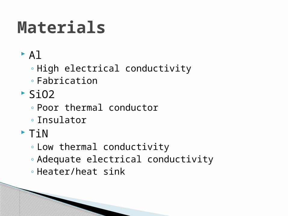
Al High electrical conductivity Fabrication
SiO2 Poor thermal conductor Insulator
TiN Low thermal conductivity Adequate electrical conductivity Heater/heat sink
Materials

Ge2Sb2Te5 (GST) High crystallization temperature Low melting point Adequate Data retention (~10 years at 80°C-
90°C)
Phase-change material

CMOS compatible fabrication techniques Minimal thermal crosstalk (65 nm nodes) Multi-bit storage possible
GST


0° to 90° Large active region smaller active region High peak RESET current lower current
26% reduction High peak temperature lower peak
temperature Larger GST area at 90°
Heat diffuses over larger area Oxide confines heat
Variation of theta angle


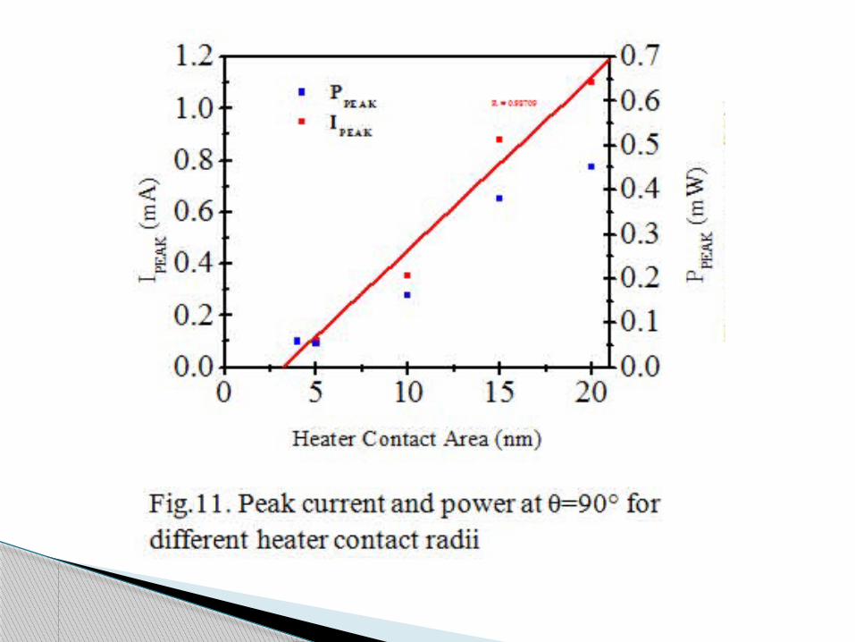
4 nm to 20 nm Constant theta angle Constant 1.0 ns voltage pulse Increase in active region size
Must amorphize entire contact area Reduction in voltage pulse
Reduction in thermal resistance (oxide) 10.5 times more RESET current
Variation of heater contact

OXIDETiN
TiN
Vpulse
Aluminum
Aluminum
5 nm
40 nm
30 nm
20 nm
100 nm
25 nm
NOTE: Geometry is not drawn to scale
GST
7 nm

Lateral cross-section: 78.54 nm2
GST thickness: 20 nm Erase time: 1.0 ns Programming voltage: 0.512 V Read voltage: 150 mV Low read current: 3.25 nA High read current:1.04 µA RESET current density: 133.7 MA/cm2
Small contact area
Specifications

Low (0) resistance = 46.2 MΩ High (1) resistance = 144.2 kΩ ~320 times less resistance 2-3 orders of magnitude Large range
Multi-bit storage
Resistance Variation

READ operation
0.00 0.25 0.50 0.75 1.00 1.25 1.500
1
2
3
4
0.00
0.05
0.10
0.15
0.20
0.25
0.30
0.35
0.40
I
Cur
rent
(nA
)
Time (ns)
Rea
d V
olta
ge (
V) V
IPEAK = 3.25 nAR = 46.2 MΩ
IPEAK = 1.04 µAR = 144.2 kΩ
0.00 0.25 0.50 0.75 1.00 1.25 1.500.0
0.2
0.4
0.6
0.8
1.0
1.2
1.4
1.6
0.00
0.05
0.10
0.15
0.20
0.25
0.30
0.35
0.40
I
Cur
rent
(uA
)
Time (ns)
Rea
d V
olta
ge (
V) V

QUESTIONS or COMMENTS?