preliminary design review analysis of a 250 … · the text of this report is devoted solely to a...
TRANSCRIPT
.A.
System Reliability Technology
Technical Report No. 5
PRELIMINARY DESIGN REVIEW ANALYSIS OF A
250-VOLT-AMPERE STATIC INVERTER
December 1965
Prepared for
Off ice of Reliability and Quality Assurance National Aeronautics and Space Administration
Washington, D. C. 20546
Under Contract NASw-905
i
E L R E S E A R C H T R I A N G L E I N S T I T U T E * D U R H A M , N O R T H C A R O L I N A
I-
https://ntrs.nasa.gov/search.jsp?R=19670016944 2018-06-04T11:26:25+00:00Z
c
' FO~EWORD
.
This report is one of a series of technical reports issued by RTI (Research Triangle Institute), Durham, North Carolina, under NASA (National Aeronautics and
Space Administration) Contract NASw-905, "Development of Reliability Methodology
for Systems Engineering".
J. E. Condon, Director, ORQA (Office of Reliability and Quality Assurance) NASA Headquarters, Washington, D. C.
The contract is administered under the direction of
The major objective of this contract is to apply probabilistic modeling techniques developed at RTI under a previous NASA contract to a NASA in-house R and
D system and t o conduct research necessary to further develop techniques appropriate
to probabilistic modeling.
and development by the Astrionics Laboratory of MSFC (Marshall Space Flight Center)
was selected as a representative NASA system for application and demonstration of
the techniques, and the majority of the technical reports in this series are
devoted to documenting results of this effort.
basic and applied i n nature, on general probabilistic modeling is documented in
several specific reports also included in this series.
A complex 250 volt-ampere static inverter under design
The additional research, both
The effort under this contract began in April 1964, and will continue for a
period of approximately two years.
Institute's Solid State Laboratory and Statistics Research Division under the general direction of Dr. R. M . Burger with W. S. Thompson serving as project leader.
The studies are being performed jointly in the
*
ii

8
PREFACE
This report is the fifth technical report of the series to be issued under Contract NASw-905. The text of this report is devoted solely to a preliminary design review analysis of the MSFC 250 volt-ampere static inverter which is being
analyzed for reliability by modeling procedures under this contract. In addition
to promoting sound engineering practices to enhance reliability, the complete
inverter analysis under the contract is concerned primarily with both performance
and life.
The analysis herein is not a complete reliability analysis of the inverter but
is presented as one type of analysis that is performed by the designer at an early
stage of the design process. The analysis is limited primarily to relatively simple hand calculations for comparing worst case operating requirements of components to their rated conditions. Such an analysis is not usually documented in this formal manner, but since it is used in this case as a basis for identifying the need for
more detailed analysis for certain portions of the circuit, it is presented for future reference to demonstrate this role.
The major portion of the study leading to this report was conducted during an
earlier phase of the contract. The major contributor in this effort was C. D. Parker.
iii

8
ACKNOWLEDGMENT
The static inverter described in this report is being developed in the
Applied Research Branch, Astrionics Laboratory, George C. Marshall Space Flight
Center, NASA, Huntsville, Alabama 35812. for permission to use the static inverter in this contract study. are due to Astrionics engineers, R. F. Harwell, W. J. Kreider, and A. E. Willis for their helpful discussions on the inverter operation which contributed greatly
to this report.
Appreciation is extended to this group Special thanks
iv

TABLE OF CONTENTS
FOREWORD
PREFACE
ACKNOWLEDGEMENT
1. I n t r o d u c t i o n
2 . Element Analyses
2 .1 Six-Volt Power Supply
2.2 E l e c t r o n i c Switch
2 .3 The Primary O s c i l l a t o r
2 . 4 The Frequency Countdown C i r c u i t
2 .5 The Clock P u l s e Amplif ier
2 .6 The P u l s e Sequence Generator
2.7 The Timing P u l s e Amplif ier
2 .8 Power Converter S t a g e
2 .9 The Output C i r c u i t
2.10 The 20-Volt Regulated Supply
2 .11 Magnetic Amplif ier Driver
2.12 Magnetic Amplif ier C i r c u i t
2.13 Voltage E r r o r Detec t ion C i r c u i t
2 .14 Over-Current P r o t e c t i o n C i r c u i t
2.15 Primary Voltage Regulator
3. An Observed F a i l u r e Mode
4. Some Observed Performances
5. A Summary of Conclusions
6 . References
Page ii
iii
i v
1
3
3
10
13
13
16
20
20
28
34
37
38
41
45
47
52
63
66
70
74

1. In t roduc t ion
The f u n c t i o n a l ope ra t ion of a complex s t a t i c i n v e r t e r w a s desc r ibed i n d e t a i l
i n Reference 1. This i n v e r t e r i s under development i n t h e A s t r i o n i c s Laboratory
a t George C. Marshal l Space F l i g h t Center and is designed as a space borne a c
power supply t o convert 28 vdc i n t o a three-phase, 115 vac , 400 cps , s i n u s o i d a l
ou tpu t w i th a load capac i ty of 250 va. The i n v e r t e r design is be ing used a s a
t e s t v e h i c l e under t h i s c o n t r a c t e f f o r t f o r a p p l i c a t i o n o f t he r e l i a b i l i t y method-
ology being developed.
I n the design and development of a space equipment t h e even tua l goa l i s an
equipment design providing adequate performance c a p a b i l i t y and having s u f f i c i e n t
l i f e t o perform t h e intended funct ions f o r t h e du ra t ion o f t h e mission. Thus
r e l i a b i l i t y as an important design cr i ter ia i s w e l l e s t a b l i s h e d .
I n a thorough a n a l y s i s of equipment f o r r e l i a b i l i t y , c e r t a i n procedures are
inhe ren t . Having e s t a b l i s h e d an i n i t i a l c i r c u i t con f igu ra t ion a s a b a s i s f o r
performing c e r t a i n func t ions , t he c i r c u i t des igne r proceeds wi th an i t e r a t i v e
review p rocess of t he c i r c u i t with emphasis on performance and l i f e . This process
e n t a i l s computation of c e r t a i n component requirements and comparison wi th component
r a t i n g s t o a s s u r e t h a t t h e component c a p a b i l i t i e s are n o t exceeded. Such an
a n a l y s i s serves t o i d e n t i f y needed improvements i n the design, and r e s u l t s may l e a d
t o a c t i o n s such as ; s e l e c t i o n o f b e t t e r components, change i n component purchase
s p e c i f i c a t i o n s , c i r c u i t r edes ign o r modif icat ion, s p e c i a l q u a l i f i c a t i o n t e s t i n g ,
n e g o t i a t i o n o f change i n i n t e r f a c e c h a r a c t e r i s t i c s with o t h e r equipments, and
i d e n t i f i c a t i o n of l i m i t a t i o n s i n t h e c i r c u i t a p p l i c a t i o n . Seldom are ana lyses
a t t h i s s t a g e of t h e design documented i n a manner more formal than t h e d e s i g n e r ' s
notebook.
A prel iminary design review of t h i s type has been performed f o r t h e s t a t i c
i n v e r t e r c i r c u i t r y . The purpose of t h i s r e p o r t i s t o p r e s e n t t h i s a n a l y s i s
p r i m a r i l y t o i l l u s t r a t e t h e con t r ibu t ions such a review can make toward t h e design
of r e l i a b l e equipment.
a n a l y s e s t o be performed wi th in the framework of t he r e l i a b i l i t y methodology
b e i n g developed.
r e l i a b i l i t y a n a l y s i s ; however, t h e a n a l y s i s was performed w i t h t h e r e l i a b i l i t y as
t h e p r i n c i p l e c r i t e r i o n f o r a success fu l design. P r i n c i p a l l y , t h e design review
i s based upon t h e i n v e r t e r s p e c i f i c a t i o n s and t h e component p a r t s c h a r a c t e r i s t i c s
as pub l i shed by t h e component manufacturers. Often these are inadequate and o t h e r
It a l s o serves as a b a s i s f o r i d e n t i f y i n g more d e t a i l e d
It i s emphasized t h a t t h i s review i s n o t presented as a complete
c r i te r ia a r e used as a b a s i s f o r eva lua t ing t h e design; f o r example, measured
.
2
component c h a r a c t e r i s t i c s .
t h e a n a l y s i s without knowing f o r c e r t a i n t h a t design c r i t e r i a unknown t o the reviewer in f luenced o r even d i c t a t e d c e r t a i n d e c i s i o n s . To consider t h e ques t ions
r a i s e d by a design review such as t h i s ; however, can on ly enhance and n o t d e t r a c t from a r e l i a b l e equipment design. The c a l c u l a t i o n s i n t h i s a n a l y s i s are simple
and w i l l be obvious t o most r eade r s . I n some cases u n i t s may be haphazardly pre-
s en ted , b u t a l s o w i l l be obvious. For each element reviewed, worst-case loads and
i n p u t s a r e u s u a l l y assumed without cons ide r ing p o s s i b l e nega t ive c o r r e l a t i o n s , and
a l l b u t t he most obvious c o n s i d e r a t i o n s a r e included. Also, worst-case parameter
va lues are used when t h e expected v a r i a t i o n i s s i g n i f i c a n t ,
made of t h e s t a t i c i n v e r t e r breadboard i n t h a t v o l t a g e and c u r r e n t l e v e l s determined
from the review were compared wi th observed va lues .
Design dec i s ions are a l s o quest ioned f r e e l y throughout
Extensive use has been
Each f u n c t i o n a l c i r c u i t o r major element of t h e i n v e r t e r is d i scussed
s e p a r a t e l y i n Sec t ion 2 a long wi th some a d d i t i o n a l f a c t o r s t h a t a r e considered
p e r t i n e n t t o the r e l i a b i l i t y .
suggested f o r t h e purpose of improving the r e l i a b i l i t y o f t h e i n v e r t e r .
i s devoted t o more de t a i l d i scuss ion of an observed f a i l u r e mode of cons ide rab le
i n t e r e s t t h a t was p red ic t ed by t h e design review and la ter observed wi th t h e
breadboard c i r c u i t . Sec t ion 4 p r e s e n t s , f o r r e f e r e n c e , a summary of observed
performance wi th the breadboard c i r c u i t . F i n a l l y , s e c t i o n 5 inc ludes a summary of
t h e f i n d i n g s of t h i s des ign review and i d e n t i f i c a t i o n of more d e t a i l e d ana lyses t o
be performed wi th in t h e framework of t he r e l i a b i l i t y methodology under development.
With t h e pub l i ca t ion of t h i s r e p o r t some of t h e a d d i t i o n a l ana lyses are being per-
formed while some a r e a l r eady complete.
r e p o r t s o r t he f i n a l r e p o r t
For example, some c i r c u i t con f igu ra t ion changes are
Sec t ion 3
These w i l l be publ ished i n f u t u r e t e c h n i c a l

2. Element Analyses
2 . 1 Six-Volt Power Supply
A schematic diagram o f t h e s i x - v o l t power supply i s presented i n Figure 1.
The s i x - v o l t power supply func t ions t o provide r e g u l a t e d dc t o elements of t he
t iming s e c t i o n as i l l u s t r a t e d i n Fig. 2.2 of Reference 1.
(1) Required Ex te rna l Load
Estimates of max imum loads f o r t h e va r ious elements supp l i ed by t h e s ix- v o l t supply are as follows.
t o be 6 .5 vdc as de r ived from the 7.5 v zener vo l t age of CR145 o r CR139 through
d iodes CR140 or CR146 having approximately a 1 v forward drop.
The output v o l t a g e f o r t hese c a l c u l a t i o n s i s assumed
(a) Closed E l e c t r o n i c Switch (see Fig. 5)
= 21 mw. 2KQ
(b) Open E l e c t r o n i c Switch (see Fig. 5)
422 Base C i r c u i t :
424 and 425 Base C i r c u i t s :
n
(c) Primary O s c i l l a t o r (see Fig. 6)
GSL = 7.5 mw. 5.6KQ
(d) D i s s ipa t ion i n 12 T. I. In teg ra t ed C i r c u i t s
a t 7 mw each (from T. I. data)
7 mw x 1 2 = 84 mw.
(e) Clock Pulse Amplifier (see Fig. 9)
Co l l ec to r C i r c u i t :
n
3

U a 3 0 m
I
In hl
m U ,-i
(d E U m u a (I) E .c 0
0 4
a 3 v1 u 4 0 3 In
I-
h a a 3 VI
4
U rl 0
X 7
a, Fc 3 M
4

Base Circuit:
1 (4.5v) 2 - - x 1KQ - 2
(f) Magnetic amplifier drive (see Fig.
10 m.
17)
(g) Timing pulse amplifier drive (see Fig. 11)
Diodes : -v x 1 . 5 ~ x 6 = 36 mw. 619 ohm
x 6 = 60 m. (2 .SV)~ 619 ohm Resistors :
Total external load 405 mw;
at 6.5 volts, the load current is
-= 405 lllW '' 62 ma. 6.5 v
ry Measured 6V supply current = 65 ma.
(2) Internal Part Requirements The following estimates of internal power dissipation are based primarily
on worst-case conditions and, therefore, are conservative. Due to the internal redun- dancy there is a duality of components, and the power dissipation depends on the
mode of operation with regard to redundancy. 1 1 4 10 (a) Resistors R83, R84 [- watt, derated to -watt @ 100°C]
Bias Circuit f o r the Inactive Channel;
This represents an additional load on the active channel of
- = 91 mw 12 ma. 7.5 v
Bias Circuit for the active channel: power dissipation is negligible
(b) Resistors R81, R82 [200 ohm, 10 watt, derates to 7 watts at 100°C]
Inactive channel : 3
5
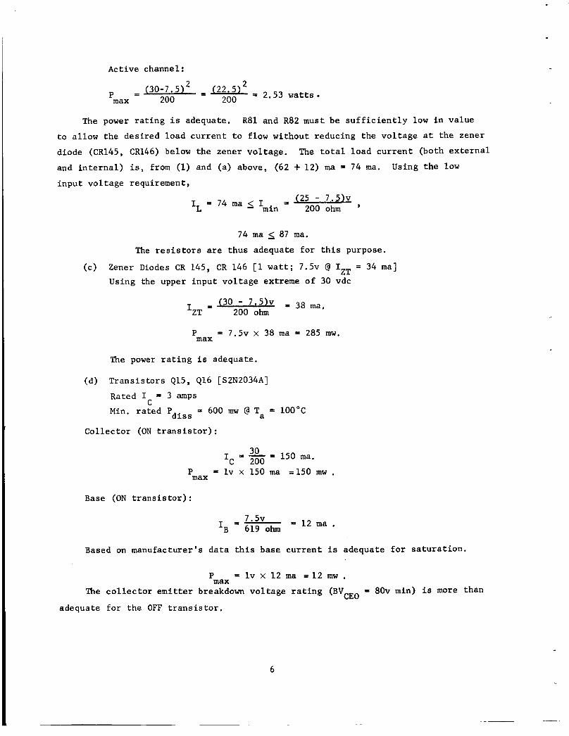
Active channel:
2 = 2.53 watts 30-7.5) - -
200 200 P = ( max
The power r a t i n g i s adequate. R81 and R82 must be s u f f i c i e n t l y low i n va lue
t o a l low the des i red load c u r r e n t t o flow without reducing the vo l t age a t the zener
diode (CR145, CR146) below the zener vol tage . The t o t a l load c u r r e n t (both e x t e r n a l
and i n t e r n a l ) is , from (1) and (a ) above, (62 + 12) ma = 74 ma. Using the low
input vo l t age requirement,
25 - 7 . 5 ) ~ 200 ohm ' I~ = 74 ma 5 Imin = (
74 m a 5 87 ma.
The r e s i s t o r s are thus adequate f o r t h i s purpose.
(c) Zener Diodes CR 145, CR 146 [l w a t t ; 7 . 5 ~ @ IZT = 34 ma] Using the upper inpu t vo l t age extreme o f 30 vdc
P = 7 . 5 ~ x 38 m a = 285 mw. max
The power r a t i n g i s adequate.
(d) Trans i s to r s Ql5, 416 [S2N2034A]
Rated I = 3 amps
Min. r a t ed Pdiss = 600 mw @ Ta = 100°C C
Col l ec to r (ON t r a n s i s t o r ) :
30 150 ma. % = 2 0 0 = P = l v x 150 m a =150 mw , max
Base (ON t r a n s i s t o r ) :
= 7*5v 'B 619 ohm = 12 ma .
Based on manufacturer ' s da t a t h i s base c u r r e n t i s adequate f o r s a t u r a t i o n .
= l v x 12 m a = 12 mw . 'max The c o l l e c t o r emitter breakdown vo l t age r a t i n g (BV = 80v min) is more than CEO
adequate f o r the OFF t r a n s i s t o r ,
6
( e ) Diodes CR139, CR140 [400 ma, Vf < 1 v o l t ]
The diodes a r e adequate to conduct t he load c u r r e n t o f 71 ma.
P = l v < 71 m a = 71 mw. max
1 1 10
( f ) R e s i s t o r s R27, R28 [;; watt , de ra t ed t o - w a t t @ 100°C]
The power d i s s i p a t i o n i s n e g l i g i b l e .
To ta l i n t e r n a l power d i s s i p a t i o n 7.6 watts.
(3) Conclusions
From the p re l imina ry obse rva t ions i t i s g e n e r a l l y concluded t h a t t he s i x - v o l t
power supply i s adequately designed t o supply the s i x - v o l t load under a l l con-
d i t i o n s of t i m e , load, i n p u t s , and temperature extremes. However, t h e c i r c u i t does
d i s s i p a t e more power than i s necessary, and i t appears t h a t t h e redundancy scheme
can be dup l i ca t ed less expensively, The e f f i c i e n c y of t he s i x - v o l t supply can be
e s t i m a t e d t o be a s low a s
'U 405 mw 11 = - x 100% = 405 + 7600 x 'in
The redundancy a s s u r e s t h a t t h e s i x - v o l t supply
'u
100% = 5.3%.
w i l l n o t f a i l i f CR145 o r CR146
s h o r t c i r c u i t o r i f R 8 1 o r R82 open. I f CR146 o r CR147 open c i r c u i t o r i f R81 o r
R82 s h o r t c i r c u i t , then the s i x - v o l t supply w i l l be abnormally high and the system
w i l l f a i l .
It i s suggested t h a t t h e same redundancy can be achieved by simply removing
t h e t r a n s i s t o r s and t h e i r b i a s i n g c i r c u i t s . This w i l l reduce t h e component count
b u t cause both zener diodes t o conduct continuously. Unless the zener diode f a i l u r e
' p r o b a b i l i t y i s s i g n i f i c a n t l y increased i n the zener breakdown region, i t w i l l n o t
s i g n i f i c a n t l y inc rease t h e p r o b a b i l i t y o f f a i l u r e of t he system.
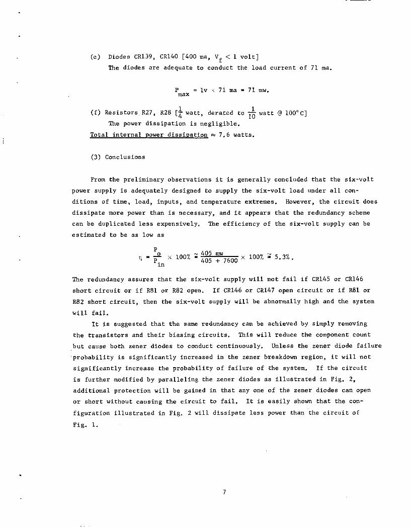
i s f u r t h e r modified by p a r a l l e l i n g the zener diodes as i l l u s t r a t e d i n Fig. 2,
a d d i t i o n a l p r o t e c t i o n w i l l be gained i n t h a t any one of the zener diodes can open
o r s h o r t without causing t h e c i r c u i t t o f a i l . It i s e a s i l y shown t h a t t he con-
f i g u r a t i o n i l l u s t r a t e d i n Fig. 2 w i l l d i s s i p a t e less power than the c i r c u i t of
Fig. 1.
I f t h e c i r c u i t
. 7
p" i n : t o 6v load
f R82 I+=- t o 6v load
Figure 2. A Modified Six-Volt Supply
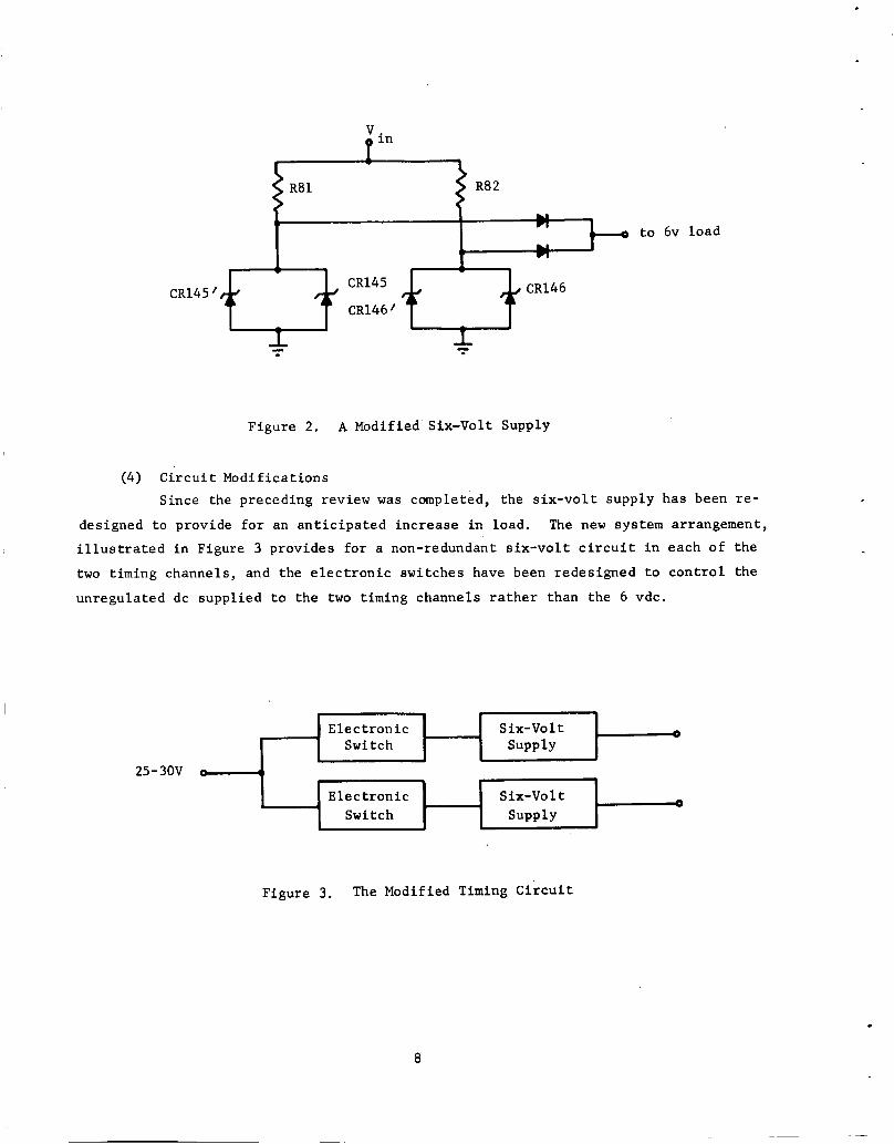
( 4 ) C i r c u i t Modif icat ions Since the preceding review was completed, t he s i x - v o l t supply has been re-
designed t o provide f o r an a n t i c i p a t e d inc rease i n load. The new system arrangement,
i l l u s t r a t e d i n Figure 3 provides f o r a non-redundant s i x - v o l t c i r c u i t i n each o f t h e
two timing channels, and the e l e c t r o n i c switches have been redesigned t o c o n t r o l t he
unregulated dc suppl ied t o t h e two timing channels r a t h e r than the 6 vdc.
s ix-vo 1 t H supply E l e c t r o n i c
Switch
25-30V o 4 1
E l e c t r o n i c s ix-vo 1 t Switch Supply
0
Figure 3. The Modified Timing C i r c u i t
8
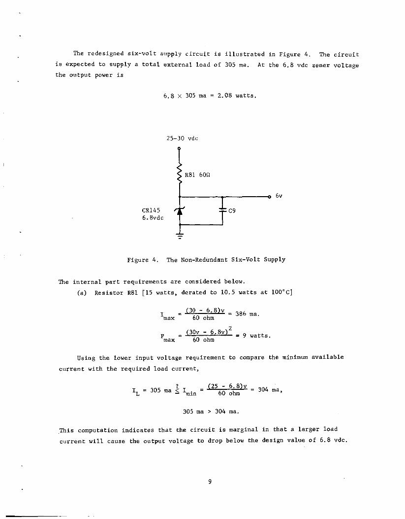
The redes igned s i x - v o l t supply c i r c u i t i s i l l u s t r a t e d i n Figure 4 . The c i r c u i t
A t the 6 .8 vdc zener vo l t age i s expected t o supply a t o t a l e x t e r n a l l oad of 305 m a .
the ou tpu t power i s
6 .8 x 305 ma = 2.08 wat ts .
25-30 vdc
R81 60s2 i Figure 4 . The Non-Redundant Six-Volt Supply
The i n t e r n a l p a r t requirements are considered below.
(a) Res i s to r R 8 1 [15 w a t t s , dera ted t o 10.5 w a t t s a t 100°C]
Using the lower i n p u t vo l t age requirement t o compare the minimum a v a i l a b l e
c u r r e n t w i th the r equ i r ed load cu r ren t ,
25 - 6' 8)v t 304 m a , 7
60 ohm IL = 305 m a 2 Imin = ' 305 m a > 304 m a .
Th i s computation i n d i c a t e s t h a t the c i r c u i t i s marginal i n t h a t a l a r g e r load
c u r r e n t w i l l cause the output vo l tage t o drop below the design va lue of 6.8 vdc.
9

(b) Zener diode, CR145 [ l o w a t t ; 6.8 v o l t s ]
= (386 - 305)ma = 81 ma. IZT,max
P = 6.8 x 81 ma = 550 mw. max
(c, Capacitor C9
Since the r i p p l e on the ou tpu t i s expected t o be small , t h e power
d i s s i p a t i o n i n the c a p a c i t o r i s considered n e g l i g i b l e .
To ta l i n t e r n a l power d i s s i p a t i o n 2: 9.55 wa t t s .
From t h e above a n a l y s i s t h e c i r c u i t is concluded t o be marginal i n i t s a b i l i t y t o d e l i v e r t he r equ i r ed o u t p u t c u r r e n t a t t he design v o l t a g e under low i n p u t
v o l t a g e cond i t ions .
Fig. 3' i s e s s e n t i a l l y the same, an a d d i t i o n a l drop of 0.5 t o 1.0 vdc, i . e . , the VCE
,drop o f t h e e l e c t r o n i c switch, w i l l aggravate t h e s i t u a t i o n even more. The r e s i s t a n c e
of R81 should the re fo re be decreased t o
I f t he design of t h e new e l e c t r o n i c switch a s i l l u s t r a t e d i n
_(25 - 1 - 6 . 8 ) ~ - 17*2v x 57 ohm. 300 ma 300 m a
This , o f course, w i l l i nc rease the i n t e r n a l power d i s s i p a t i o n s l i g h t l y .
For t h e design as shown i n F ig , 4 t he e f f i c i e n c y a t maximum power o u t p u t i s
x 100 = 17.8% 2.08 w (2.08 + 9 . 5 5 ) ~ n =
which i s an improvement i n t h i s regard over t he o r i g i n a l design.
With the appropr i a t e mod i f i ca t ion i n t h e r e s i s t a n c e o f R 8 1 t he c i r c u i t i s
considered of sound design and adequate f o r s e rv ing i t s intended funct ion.
2 . 2 The E lec t ron ic Switch
(1) Closed Switch Operation
The e l e c t r o n i c switch i s shown schemat i ca l ly i n Fig. 5. When t h e switch - i s c losed , i npu t s q5 and q5 and t h e s i x - v o l t supply t o t h e primary o f T9 a r e missing.
T r a n s i s t o r 422 i s forward b i a sed through R57, connect ing t h e s i x - v o l t supply t o
the load.
(a) T rans i s to r 422, S2N1132
Rated IC = 600 ma ,
Rated Pdiss = 600 mw,
10
rn c %
h d a a 5 m
I I E 0 &I k
. . !+
11

I requirement = 65 m a (es t imated load c u r r e n t ) ,
The base c u r r e n t i s e s t ima ted t o be C
= 2.5 ma. - 'B - 2KQ
From manufac tu re r ' s da t a , i t i s concluded t h a t IB = 2.5 ma i s an
adequate base d r i v e f o r maintaining s a t u r a t i o n .
422 ope ra t e s a s a c losed o r an open swi t ch f o r long per iods.
fo re , t he power d i s s i p a t i o n i s n e g l i g i b l e .
There-
(2) Open Switch Operation
The inpu t s q5 and 45 i n Fig. 5 a r e complimentary squarewave s i g n a l s . A s
determined i n Sect ion 2.6, t he high and low v o l t a g e l e v e l s a r e approximately 3.5
and ze ro v o l t s , r e spec t ive ly .
( a ) T r a n s i s t o r 422 (2N718A)
The r equ i r ed c o l l e c t o r c u r r e n t i s
6v
4Kfi X (7) IC = = 6 ma.
For t h i s c o l l e c t o r c u r r e n t , t he base c u r r e n t r e q u i r e d f o r s a t u r a t i o n
i s
- 6ma IB - - = 0 . 3 m a (from worst-case h ), 20 FE
IB = 0.12 ma (from measured c h a r a c t e r i s t i c s ) .
The e s t ima ted base c u r r e n t i s
(3.5 - 0 . 8 ) ~ .8v - - = 1.2 ma, - 'B - 2KQ 7.5Kn
and i s more than adequate.
(b) Transformer T9, MSFC NR1191 (core; Magnetics, Inc . , Orthonal, 51056-2A)
N = 700 t u r n s P
-6 2 A f e = 4 . 3 x 10 m
b = AfeBs 4 .3 X m2 x 1.45 web/m
= 6.24 x web.
= 2OS = 12.5 x web "max
12
For t h e 400 cps. ope ra t ions ,
x 1.25 x = 1 0 . 8 ~ A @ = G A T = - e
7 00
Thus the transformer co re i s adequate.
web < 1 2 . 5 ~ web = A@max
1 (c) R e s i s t o r s R52, R59[ wat t s , de ra t ed t o 10 @ 100°C]
R
4
x .01 wa t t s . v2 (4.5v) 2KQ Maximum d i s s i p a t i o n i s - 5
(d) Capaci tor C9 [15v, 150pf . l
This c a p a c i t o r is e s s e n t i a l i n t h a t it removes the 400 cps s p i k e s introduced
I t s by t h e a l t e r n a t e channel switch and t h e 4.8 kc r i p p l e from t h e s i x - v o l t bus.
capaci tance and vo l t age r a t i n g s a r e adequate.
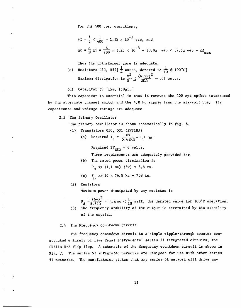
2.3 The Primary O s c i l l a t o r
The primary o s c i l l a t o r i s shown schemat i ca l ly i n Eig. 6.
(1) T r a n s i s t o r s 430, 431 (2N718A)
(a) Required I =~ =1.1 ma. c 5.62Kn
Required BVCEO = 6 v o l t s .
These requirements a r e adequately provided f o r .
The r a t e d power d i s s i p a t i o n i s
Pd >> (1.1 ma) (6v) = 6.6 mw. (b)
(c) f >> 10 x 76.8 kc = 768 kc. B
(2) R e s i s t o r s
Maximum power d i s s i p a t e d by any r e s i s t o r i s n
1 ' OL = 6.4mw < 10 w a t t , t he de ra t ed value f o r 100°C operat ion. 'd =5.620
The frequency s t a b i l i t y of t h e ou tpu t is determined by t h e s t a b i l i t y
o f t h e c r y s t a l . ( 3 )
2.4 The Frequency Countdown C i r c u i t
The frequency countdown c i r c u i t i s a simple r i p p l e - through counter con-
s t r u c t e d e n t i r e l y o f f i v e Texas Instruments ' series 51 i n t e g r a t e d c i r c u i t s , t he
SN511A R-S f l i p f lop. A schematic of t he frequency countdown c i r c u i t is shown i n
Fig. 7. The series 51 i n t e g r a t e d networks are designed f o r use with o t h e r series
51 networks. The manufacturer states t h a t any series 51 network w i l l d r i v e any
13
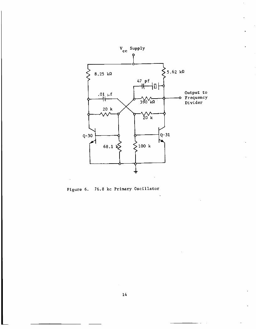
Figure 6. 76.8 kc Primary Oscillator
14

1 $ 8
1 I w
I u-
rn F F
,!x a
7 t -
o m 4 u
7
e-
u . C q H
t
V M 3 a Q )
' 0 k co .? d u n
t r I C '
* - *
w N 4 h h F4
t t 9 V 24 \o
U *rl 5 V k
1 -
I - w
I C T
a3 h
*- c4 h a
t I
V 24 d 00 m
b
15

o t h e r network i n the series, and f u r t h e r c i t e s i n r e fe rence 2 the r ipple- through
counter used i n the s t a t i c i n v e r t e r as a t y p i c a l a p p l i c a t i o n . Unless a s tudy i s
made of t he i n t e g r a t e d networks, a design review of equipment us ing t h e networks
i s l i m i t e d t o e s t a b l i s h i n g t h a t t he design conforms t o c e r t a i n a p p l i c a t i o n r u l e s ,
and t h a t i n p u t s and ou tpu t t o o t h e r equipment are wi th in the range of va lues s t a t e d
by t h e manufacturer t o be s a t i s f a c t o r y .
The a p p l i c a t i o n r u l e s e s t a b l i s h e d by t h e manufacturer are concerned o n l y with
in t e rconnec t ions between the series 51 i n t e g r a t e d networks, Inpu t and ou tpu t
c h a r a c t e r i s t i c s a r e given i n r e fe rence 3 and these c h a r a c t e r i s t i c s are used t o
assess t h e c o m p a t i b i l i t y o f non- se r i e s 51 i n p u t s and ou tpu t s .
fol lower ou tpu t c h a r a c t e r i s t i c s published i n r e f e r e n c e 3 a r e reproduced i n Fig. 8
along with t h e ou tpu t c h a r a c t e r i s t i c s o f s e v e r a l u n i t s measured i n the laboratory.
A l l of t he u n i t s e x h i b i t e d a lower ou tpu t impedance than t h a t claimed by the manu-
f a c t u r e r . I n the fol lowing s e c t i o n s of t h i s r e p o r t , t he o u t p u t c h a r a c t e r i s t i c s from
r e f e r e n c e 3 a r e used f o r worst-case analyses . Because of t h e low switching f r equenc ie s
involved, switching t r a n s i e n t times a r e considered of no concern i n t h e frequency
d i v i d e r c i r c u i t .
The SN511A emitter-
One o t h e r concern i s the power d i s s i p a t i o n c a p a b i l i t i e s of t he SN511A. A t
+25*C t h e u n i t s a r e r a t e d t o d i s s i p a t e 50 mw and a c t u a l l y d i s s i p a t e approximately
7 mw with ze ro fan out . When d r i v i n g a t iming pu l se a m p l i f i e r (TPA), a s desc r ibed
i n s e c t i o n 2.7, a t 25°C and ze ro frequency (with t h e 28 v o l t s removed from t h e TPA),
the SN511A d i s s i p a t e s approximately 20 mw (from l a b o r a t o r y measurements). The
a p p l i c a t i o n r u l e s a r e s t a t e d f o r the -55°C t o +125"C temperature range, b u t i t i s
n o t known how the d i s s i p a t i o n c a p a b i l i t y d e r a t e s w i th i n c r e a s i n g temperature. For
the purposes of t h i s review, i t i s assumed t h a t r a t e d power d i s s i p a t i o n w i l l n o t be
exceeded a t any temperature i f the q and 4 o u t p u t s are a minimum, i.e., a DC fan
o u t of 1, and the emit ter fol lower ou tpu t s , q* and 4" o p e r a t e i n the lower h a l f of
t he ou tpu t c h a r a c t e r i s t i c s de f ined i n r e f e r e n c e 3 , i.e., below p o i n t "A" i n Fig. 8.
A s was pointed o u t i n an e a r l i e r paragraph, t h e frequency countdown c i r c u i t
conforms t o a l l t h e series 51 a p p l i c a t i o n r u l e s . The i n p u t from t h e primary
o s c i l l a t o r is s a f e l y wi th in the wide range of s a t i s f a c t o r y i n p u t s both i n frequency
(76.8kc) and pulse amplitude (6 v o l t s maximum). The o u t p u t s from t h e frequency
countdown c i r c u i t d r i v e the magnetic a m p l i f i e r d r i v e c i r c u i t and t h e c lock pu l se
a m p l i f i e r , and these ou tpu t s w i l l be considered i n paragraphs d i s c u s s i n g t h e s e two
e lemen ts . 2.5 The Clock Pulse Amplif ier
The c lock pulse a m p l i f i e r (CPA) and i t s p o s i t i o n r e l a t i v e t o t h e
16

10.0
8.0
I
U e a, k k 3 u U 1 a U 3 0
6.0
4.0
2 . 0
0
Output Voltage - v o l t s
Figure 8. Output Characteristics of SN511A
1 . Manufacturer published data. 2. 4.8 kc operation a t 125"C--spread in data r e s u l t s from changing load on a l ternate emitter follower from no-load t o equal load. 3 . 4.8 kc operation--room temperature. 4 . "d-c" charac ter i s t i c obtained from trans is tor curve tracer. 5 . 'Id-c" charac- t e r i s t i c s from a second unit.
17

frequency countdown c i r c u i t and t h e pulse sequence genera tor (PSG) a r e shown i n
F igu re 9 .
1~ ohm and an output impedance of approximately 360 ohms.
ou tput of t h e frequency countdown c i r c u i t , and i t supp l i e s a 4 .8 kc c lock p u l s e t o
t h e PSG a t approximately 1.5 v o l t s .
This common emitter a m p l i f i e r has an input impedance of approximately
I t s input i s t h e 4.8 kc
A cons ide ra t ion o f t h e CPA design fo l lows .
(1) T rans i s to r 428 (2N718A)
Required BV = 6 v o l t s . CEO
Rated BVCEO = 50 v o l t s .
Required I = 6v/1.5KR = 4 ma << Rated IC. C
Required Power Di s s ipa t ion = 1 /8 x 6v x 4 ma = 3 mw.
Required f 10 x 4.8 kc = 48 kc.
Rated fT = 80 mc.
B
R4 6 - N 1
i
Pulse Sequence
R4 7 Genera t o r
475 n
c
Clock Pulse
Figure 9. Clock Pulse Amplifier
From measured 2N718A c o l l e c t o r c h a r a c t e r i s t i c s , t h e base c u r r e n t r equ i r ed f o r
s a t u r a t i o n i s
IB = 0.08 ma ;
from a worst-case h computation, t he requi red base c u r r e n t is FE
IB = 4 ma/2O = 0.2 m a .
18
The es t imated base cu r ren t i s
= 2.5 ma (3.5 - l )v 'B ' 1KQ
1 1 (2) Res i s to r s [All wa t t , de ra t ed t o - wat t (3 100°C]
The maximum power d i s s i p a t e d by any r e s i s t o r i s
10
1 2 - = - - (6v) v2 R 1KQ 10
- 36 mw < - watt.
(3) The output vo l t age amplitude i s determined by t h e v o l t a g e d iv ide r formed
by R42 and R47 and the load. I t s maximum value is
- - 6v *475 = 1.44 v o l t s . "out 1.97
There have been unpublished r e p o r t s of d i f f i c u l t i e s experienced wi th t h e
SN511A u n i t s when t h e clock pu l se inpu t amplitude i s too high, and t h e CPA i s
appa ren t ly , i n p a r t , a response t o such experiences. It does perform t h e func t ion
of reducing t h e clock pu l se input t o t h e SN511A u n i t s i n t h e p u l s e sequence genera tor
(PSG) from 4.5 v o l t s t o 1 .5 v o l t s , approximately. It seems c l e a r t h a t , i f t he
c lock pu l se input t o an R-S f l i p f l o p is high wi th r e spec t t o t h e R and S term-
i n a t i o n s , t h e r e s u l t i n g s t a t e o f t he f l i p f l o p w i l l be inde termina te . Such a
cond i t ion i s n o t l i k e l y t o e x i s t i n t h e s t a t i c i n v e r t e r , however, s i n c e a l l f l i p
f l o p s a r e suppl ied from t h e same bus, and t h e R and S te rmina t ions are connected
t o SN511A ou tpu t s and t h e clock pulse inpu t s t o SN511A emi t t e r fol lower ou tpu t s .
I n t h e absence of any specific w r i t t e n r e p o r t s of u n s a t i s f a c t o r y performance
o f t he s e r i e s 51 i n t e g r a t e d c i r c u i t s due t o the amplitude of t h e clock pu l se inpu t ,
cons ide ra t ion was g iven t o t h e e l imina t ion of t h e clock pu l se a m p l i f i e r .
CPA output suppl ied the clock pulse input t o t h e PSG d i r e c t l y , t he a p p l i c a t i o n
r u l e s would be v i o l a t e d i n t h a t the fan o u t o f t h e CPA SN511A network would be s i x .
The a p p l i c a t i o n r u l e s s p e c i f y a maximum a c fan o u t of f i v e , bu t t h i s load is per-
mi t t ed over a temperature range from -55'C t o +125"C and a t c lock f requencies
g r e a t e d than 500 kc .
fan o u t of 6 i s not excess ive a t 400 cps and a t t h e lower temperature extremes.
I f t he
A s tudy of tl-e SN511A networks may i l l u s t r a t e t h a t an a c
Experimental ly , t h e clock p u l s e ampl i f i e r has been removed from one of t he
two timing channels i n t h e s t a t i c i n v e r t e r , and t h e input s i g n a l t o the ampl i f i e r
connected d i r e c t l y t o t h e ampl i f i e r load, i .e . , t h e s i x SN511A f l i p f l o p s of t h e PSG.
19

The s t a t i c i n v e r t e r breadboard has subsequent ly been caused t o o p e r a t e on t h e
a l t e r e d channel fo r extended pe r iods of t i m e and under a l l i n p u t , load and temp-
e r a t u r e extremes, No d i f f i c u l t i e s have been experienced wi th t h e t iming channel
during t h i s per iod and t h e i n v e r t e r has n o t switched from t h i s channel t o t h e
redundant channel during ope ra t ion . Consequently, i t i s concluded t h a t t h e CPA
may be unnecessary. This problem must be i n v e s t i g a t e d f u r t h e r be fo re a f i rm
recommendation can b e made f o r i t s removal from t h e c i r c u i t .
It i s noted t h a t i n an e a r l i e r v e r s i o n of t h e s t a t i c i n v e r t e r , t h e p r e s e n t
c lock p u l s e a m p l i f i e r was probably r equ i r ed f o r p u l s e shaping.
model, t h e 4.8 kc ou tpu t of t h e frequency countdown c i r c u i t supp l i ed t h e i n p u t s t o
t h e magnetic a m p l i f i e r d r i v e c i r c u i t j u s t as it does i n t h e p r e s e n t model, bu t t h e
4 . 8 kc inpu t t o the PSG was supp l i ed from a secondary winding on t h e magnetic
a m p l i f i e r d r i v e t ransformer. The c lock p u l s e winding supp l i ed a s i x v o l t P-P, 4 .8 kc
squa re wave vo l t age t h a t was symmetrical about ze ro . The CPA was necessary t o
e l i m i n a t e t h e nega t ive p o r t i o n o f t h e squa re wave and reduce t h e peak amplitude.
I n t h e ear l ier
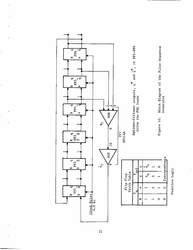
2.6 The Pu l se Sequence Generator
The pulse sequence gene ra to r (PSG) i s a Johnson Counter l o g i c c i r c u i t
c o n s i s t i n g e n t i r e l y o f s ix Texas Instruments ' SN511A networks and a Texas Ins t rumen t s '
SN514A network t o reset t h e counter . The in t e rconnec t ion of t h e s e u n i t s is
i l l u s t r a t e d i n F igu re 10.
series 51 u n i t s by t h e manufacturer i n r e f e r e n c e 2 and t h e design of t h e PSG is i n
accord wi th t h e a p p l i c a t i o n r u l e s s t a t e d i n t h a t r e f e r e n c e .
The PSG i s a l s o used as an example a p p l i c a t i o n o f t h e
The inpu t t o t h e clock p u l s e t e rmina l s o f t h e PSG SN511A networks i s w i t h i n
t h e range of values given by t h e manufacturer a s s a t i s f a c t o r y from both t h e
frequency d i v i d e r c i r c u i t and t h e CPA. The low frequency 400 cps c lock p u l s e ra te
e l imina te s switching t i m e a s a performance c o n s i d e r a t i o n . The ou tpu t of t h e PSG
w i l l be considered i n t h e next s e c t i o n d i scuss ing t h e t iming p u l s e a m p l i f i e r s .
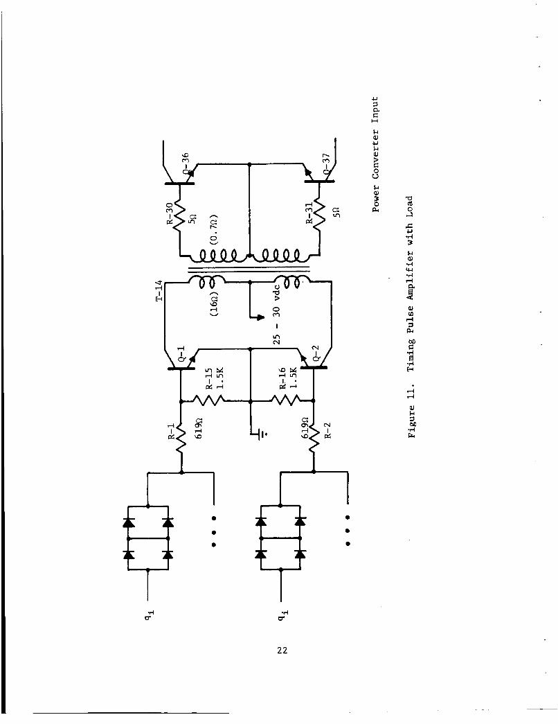
2 . 7 The Timing P u l s e Amplif ier
A schematic diagram o f a t iming p u l s e a m p l i f i e r i s shown i n F i g u r e 11.
The i n p u t s , qi and si, are complementary 400 cps. squarewaves provided by one o f
t h e series 51 i n t e g r a t e d c i r c u i t s i n t h e PSG. The primary f u n c t i o n o f t h e TPA is
t o amplify t h e s e timing pu l ses t o provide adequate base d r i v e f o r power switching
t r a n s i s t o r s 436 and 437 i n t h e power conve r t e r s t a g e s .
with t r a n s i s t o r s 41 and 42 being a l t e r n a t e l y tu rned ON and OFF a t t h e 400 cps r a t e .
The o p e r a t i o n is push-pul l
20
N
a3
0 d
z VI
3 !=.I
0 rl
aJ L4 3 M .d k
21
Ll aJ
c: PI In
I E-c
\D 4 0 T-r- W m
I m cv
a (d 0 I4

(1) T r a n s i s t o r s Q 1 , Q2 (2N2034A)
(a) Maximum c o l l e c t o r cur ren t requirement
- 3 Ov - 340 I C max
16Q + 5.7 (54) Q
i s
-., = 125 ma,
< Rated IC = 3 amps. I c max
(b) Using a 20% s a f e t y f a c t o r , i t i s requi red t h a t BVCER > 1 . 2 ~ 2 ~ 3 0 ~ = 72v.
(R = 1.5W)
Rated BVCEO = 70 v o l t s ,
Rated BVCES = 120 v o l t s .
The a c t u a l BVCER f o r R = 1.5 W i s probably nea re r t h e r a t e d BV
Also, i f a 16% s a f e t y f a c t o r was used r a t h e r than 20%, the requi red
than t h e CES
CEO ' r a t e d BV
breakdown vo l t age computed would have been 70 v o l t s . There i s cons iderable
u n c e r t a i n t y i n the 20% s a f e t y f ac to r used above. I t is a f a c t o r f r equen t ly used t o
provide f o r switching t r a n s i e n t s i n s a t u r a b l e o s c i l l a t o r c i r c u i t s and i s probably
excess ive i n t h i s ca se s i n c e switching i s not dependent on the t ransformer cores
s a t u r a t i n g . Switching t r a n s i e n t s have not been observed i n t h e l abora to ry and the
breadboard model has been operated s u c c e s s f u l l y with a supply vo l t age i n excess
o f 32 v o l t s ,
( c ) For power d i s s i p a t i o n cons ide ra t ions a gene ra l ly accepted a p p l i c a t i o n
r u l e i s t h a t t r a n s i s t o r s can switch approximately e i g h t t imes t h e Class A power
r a t i n g . The power d i s s i p a t i o n requirements a r e
2 = 0.5 watts 1 ( 3 Ov)
3 40 Pd =z 160 + 5 . 7 ( - g ) Q
Rated Pd = 8.5 w a t t s @ case temperature, Tc = 25OC,
= 5 watts @ Tc = 100°C,
= 0.6 watts @ ambient temperature, TA = 100°C.
(d) Frequency requirements are considered adequate i f t h e t r a n s i s t o r
g a i n corner frequency € ( i . e . , the frequency a t which t h e ga in i ( j o ) / i ( j u )
y i e l d s 3 db a t t e n u a t i o n from t h e f3 o r dc va lue) i s B C b
= 10 x 400 cps = 4 kc. f 0
23

The frequency f o r u n i t y ga in f$ o f t h e 2N2034A i s s p e c i f i e d by t h e manufacturer as
r a t e d f T = 1 mc minimum.
This i s known t o be s e v e r a l oc taves , say 6 , h igher than f t h e r e f o r e , 8 ;
f >> 4kc. B
(e) Base cu r ren t requi red t o s a t u r a t e t h e 2N2034A wi th IC = 125 m a i s
( i ) I < 5 ma (from STC da ta b u l l e t i n ) ,
( i i )
( i i i ) IB = 1 .8 ma (from l abora to ry measured c o l l e c t o r C h a r a c t e r i s t i c s ) .
The worst-case hFE is extremely p e s s i m i s t i c .
B
IB = 125 ma/20 = 6.25 ma (from worst-case hFE),
The u n i t s measured i n
I n t h e fol lowing t h e l abora to ry proved t o be uniform and t o have h ighe r ga ins .
ana lyses , t he IB = 1.8 m a determined from l a b measurements w i l l be used as c r i t e r i a
f o r success fu l performance.
A worst-case e s t ima te of base d r i v e cu r ren t a v a i l a b l e i s determined
a s fo l lows .
The base d r ive source is t h e SN511A i n t e g r a t e d c i r c u i t s i n t h e PSG. The
l i n e a r ou tput c h a r a c t e r i s t i c s given by the manufacturer a r e included i n F igu re 8
a s curve 1.
represented by the Thevenin's equiva len t shown below i n F igu re 1 2 .
Since the output c h a r a c t e r i s t i c s a r e l i n e a r , t h e output can be
4 . 3 vol t&
Figure 1 2 . Equivalent c i r c u i t of t h e SN511A ou tpu t c h a r a c t e r i s t i c s .
The diode-quad shown i n F igure 11 i n t h e base c i r c u i t drops 1 . 4 v o l t s a t wors t -case
temperatures (T = 0°C) and t h e 2N2034A base-emi t te r j u n c t i o n drops 0 .9 v o l t s a t
IB = 5 ma (mfg. d a t a ) , Therefore ,
24
I

(4.3 - 1.4 - .9) v = 2.4 m a , and - -
'R1 (619 + 200)Q
I = 2.4 ma - 0.6 ma = 1 . 8 m a . B
The base cu r ren t a v a i l a b l e to t h e 2N2034A as determined from t h e preceding
a n a l y s i s i s marginal a t b e s t .
i n f luence .
compared t o t h e output c h a r a c t e r i s t i c s o f some SN511A u n i t s measured i n t h e lab-
o r a t o r y . However, some measured u n i t s d id compare c l o s e l y w i t h t h e publ i shed d a t a
i n t h e reg ion o f i n t e r e s t
This a n a l y s i s i s r e a l i s t i c except f o r one modifying
The publ ished output c h a r a c t e r i s t i c s f o r t h e SN511A a r e p e s s i m i s t i c
( see F igure 8).
The marginal d r i v e condi t ions d iscussed i n t h i s s e c t i o n can be modified t o a
s a t i s f a c t o r y s i t u a t i o n by e i t h e r reducing t h e r e s i s t a n c e of R 1 and R2 o r by removing
one p a r a l l e l p a i r of diodes i n the diode coupl ing t o y i e l d only a s i n g l e diode drop.
The cognizant des ign group has a l ready r e s o r t e d t o t h e former method by reducing
t h e r e s i s t a n c e o f R 1 and R2 t o 39252.
t h i s va lue f o r r e s i s t a n c e ,
Repeating t h e preceding c a l c u l a t i o n us ing
and
- (4.3 - 1 .4 - 0 . 9 ) ~ = 3.4 ma, 'R1 - (392 + 200)Q
IB = (3.4 - 0.6) ma = 2.8 ma
which is adjudged adequate on the b a s i s measured c h a r a c t e r i s t i c s of t h e 2N2034A.
The o t h e r method o f removing one p a r a l l e l p a i r of diodes r e s u l t s i n a base
c u r r e n t es t imated as be fo re t o be
(4.3 - 0.7 - 0 . 9 ) ~ = 3,3 ma, - 'R1 - (619 + 200)Q
and
I = (3.3 - 0.6) ma = 2 .7 ma B
which i s a l s o adequate .
t h e base c i r c u i t is a po in t of content ion from t h e po in t o f view of r e l i a b i l i t y ,
Consider ing
o f t h e diode coupl ing t o be i s o l a t i o n o f t h e redundant timing channels , t h e s i n g l e
d iode p a r a l l e l p a i r h a s been shown t o be more r e l i a b l e .
The u s e o f a diode-quad vs. a s i n g l e diode p a r a l l e l p a i r i n
t h e predominant mode o f f a i l u r e t o be "opens" and t h e primary func t ion
However, o t h e r modes of
25
f a i l u r e and the effects on c i r c u i t performance must be appropr i a t e ly considered
before the quest ion i s f i n a l l y reso lved .
ga ted wi th breadboard experimentat ion being used t o compare t h e r e l a t i v e performance
of d i f f e r e n t c i r c u i t con f igu ra t ions .
This problem i s c u r r e n t l y being i n v e s t i -
The c i r c u i t modi f ica t ions as discussed above f o r ob ta in ing t h e adequate base
d r i v e and t h e r e s u l t i n g cu r ren t assumes t h a t t h e power d i s s i p a t i o n of t h e SN511A
u n i t is not exceeded.
discussed i n Sect ion 2.4, and f o r purposes of a n a l y s i s , po in t A i n F igu re 8 was
assumed t o represent t h e r a t e d power d i s s i p a t i o n .
The power d i s s i p a t i o n c a p a b i l i t i e s of the SN511A were
1 1 (2) Res i s to r s , R 1 , R2, R15, R16 [ w a t t , dera ted t o - w a t t @ loO"c] 10
The maximum power d i s s i p a t e d by any r e s i s t o r i s
'd < 392
(3) Diodes 1N645
Rated Iave = 150 ma (3 150°C ( .7v th re sho ld devices) .
The diode i s more than adequate f o r t he c u r r e n t s computed i n (1) above.
(4) Transformer T14 [Core: CARP 49; - 1 It i s requi red t h a t
where
E = 30 v o l t s ,
A T = - = 1.25 m sec , 8OOcps
N = 340 t u r n s , and
= 10 k gauss (from co re manufacturer ' s d a t a ) . Bsat
i s unknown for t h e computation above; however, experimental obse rva t ions r evea l A f e t h a t t h e t ransformer is adequate f o r t h e intended func t ion .
(5) Other Considerat ions
One o f the SN511A u n i t s i n t h e PSG is r equ i r ed t o d r i v e a 2KQ load , i . e . ,
an e l e c t r o n i c switch, i n a d d i t i o n t o the t iming p u l s e a m p l i f i e r , a very s i g n i f i c a n t
load compared t o the 'ITA load. Consequently, t h e preceding estimates o f a v a i l a b l e
26
base current must be modified for the one unit in question. Using an interative procedure, it is estimated that
- (3.5 - 1.4 - 0.9)~ = 2.1 ma, 'R1 - 619Q
= (2.1 - 6) ma = 1.5 ma, IB
- - = - 3*6v 1.8 ma, and 'SW 2KR
IFF - - IR1 + Isw = (2.1 + 1.8)ma = 3.9 ma.
which corresponds to 3.6 volts out of the driving flip-flop. it is concluded that the base drive current is not adequate (based on the 1.8 ma required).
are more optimistic than the output characteristics published by the manufacturer
and used in the preceding analysis. Without a more extensive study of the SN511A,
there is no strong justification for assuming the more optimistic, measured characteristics.
From this analysis,
In the region of 3.6 volts, all of the SN511A measured characteristics
Still using the manufacturer's published SN511A output characteristics, the following estimate is made assuming one of the diode parallel pairs is removed
from the circuit.
- (3.4 - 0.7 - 0.9)~ = 2.9 ma, 'R1 - 619R
I = (2.9 - .6)ma = 2.3 ma, B
- 3.4v Isw - - = 1.7 ma, and 2Kll
= (2.9 + 1.7) ma = 4.6 ma. IFF
Consequently, based on the required 1.8 ma base current the removal of one parallel pair of diodes will render the timing pulse amplifier satisfactory since the SN511A will adequately saturate the 2N2034A transistors with the additional load of the electronic switch.
An additional estimate of the 2N2034A base current is computed below assuming that R1 and R2 are changed to 3920.
27

- (3 .4 - 1 .4 - 0 . 9 ) ~ = 2.8 ma, 'R1 - 39251
I = (2.8 - .6) ma = 2 . 2 ma, B
- 3'4v = 1 . 7 ma, and I S W -
IFF = (2.8 + 1 .7 ) ma = 4.5 m a . \
Based on the 1 . 8 m a requi red base c u r r e n t , t h i s modi f ica t ion i s a l s o adequate.
(6) Conclusions
From the preceding cons ide ra t ions , i t i s concluded t h a t e i t h e r o f t he
modi f ica t ions i n t h e TPA design is adequate t o provide s u f f i c i e n t base c u r r e n t t o
s a t u r a t e t h e 2N2034A t r a n s i s t o r s . The o r i g i n a l design was marginal a t b e s t f o r t h e
TPA u n i t s t h a t were dr iven a s the only load from an SN511A network, and inadequate
i n t h e s i n g l e case i n which t h e d r iv ing SN511A network was a l s o loaded by t h e
e l e c t r o n i c switch. The preference of t h e two modi f ica t ions cons ider ing both
performance and l i f e i s being i n v e s t i g a t e d .
It i s assumed he re t h a t t h e added load represented by removing a diode p a i r
o r reducing R 1 and R2 w i l l no t cause t h e d r iv ing SN511A u n i t s t o exceed t h e i r r a t e d
d i s s i p a t i o n , s ince the opera t ing po in t is below "A" i n F igure 8 .
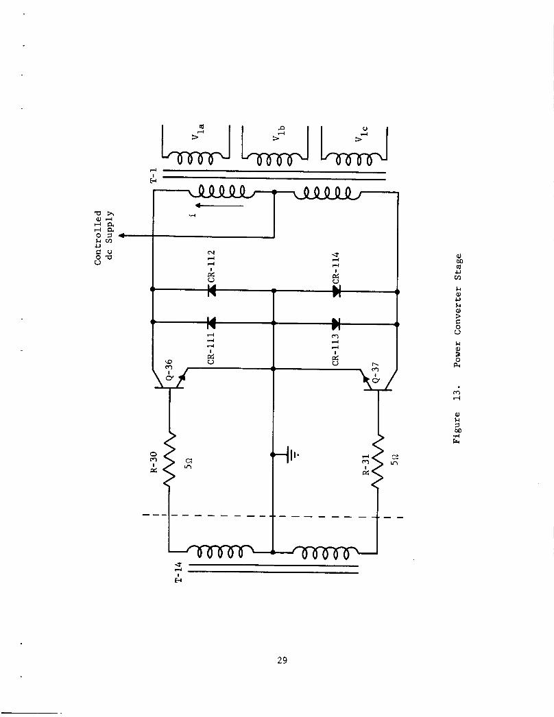
2.8 Power Converter Stage
F igure 13 i s a schematic diagram of one of t h e s i x power conver te r s t a g e s .
Each s t a g e must convert an equal amount of power and, i f an e f f i c i e n c y of 80% i s
assumed f o r t he power s e c t i o n of t h e i n v e r t e r , each s t a g e must convert approximately
(1) T r a n s i s t o r s 436,
(a ) T rans i s to r s
437 (2N1016D)
436 and 437 must block twice t h e maximum c o n t r o l l e d dc
supply vo l t age . Adding a 20% s a f e t y f a c t o r , i t is r equ i r ed t h a t
BVCEO = 2 x 23 x 1 . 2 = 55 v o l t s .
Rated BVCEO > 200 v o l t s t o 1 5 O o C .
28
I
c o o m u N rl I I-l
a, M (d u
LA
k P) & Ll a, 3 c 0 V
29
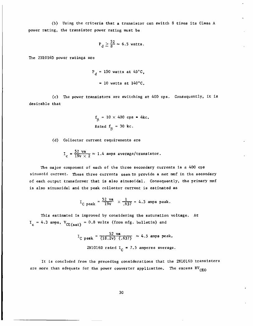
(b) Using the criteria that a transistor can switch 8 times its Class A
power rating, the transistor power rating must be
52 Pd 2 8 = 6.5 watts.
The 2N1016D power ratings are
P = 150 watts at 45"C,
= 10 watts at 140°C.
d
(c) The power transistors are switching at 400 cps. Consequently, it is desirable that
f = 10 x 400 CPS = 4kc.
Rated f = 30 kc. B
B
(d) Collector current requirements are
I = 52 va 0 1.4 amps average/transistor. c 19v x 2
The major component of each of the three secondary currents is a 400 cps sinusoid current.
of each output transformer that is also sinusoidal.
is also sinusoidal and the peak collector current is estimated as
These three currents seem to provide a net mmf in the secondary Consequently, the primary mmf
x - = = - 4.3 amps peak. 52 va IC peak 19v .637
This estimated is improved by considering the saturation voltage. At
= 0.8 volts (from mfg. bulletin) and 'CE (sat) IC = 4.3 amps,
* 4.5 amps peak.
5 amperes average.
- 52 va - IC peak (18.2~) (.637)
2N1016D rated IC = 7
It is concluded from the preceding considerations that the 2N1016D transistors are more than adequate for the power converter application. The excess BVCEO
30

r a t i n g a l s o c o n t r i b u t e s t o an increased V and, consequent ly , i nc reased power
l o s s , b u t the inc rease is considered i n s i g n i f i c a n t . CE(sat)
(e) Consider t he 2N1016D base d r i v e c i r c u i t .
The minimum N - i n t he R1020 primary i s do d t
= 23v, 25v - 'CE(sat) - IC RR1020
and IC r e f e r t o Q 1 and 42 i n the TPA u n i t . Consequently, the 436 CE(sat) where V
base d r i v e c i r c u i t can be represented as shown below. , & (2N 1 0 1 6 D
R30 plus I t r a n s f orrner I
Using a worst-case value f o r V of 1.1 v o l t s , BE
13.65 - 1 .1 )~ = = 450 ma. I B 5.7Q
From the 2N1016D c o l l e c t o r c h a r a c t e r i s t i c s t h e base c u r r e n t r equ i r ed t o
s a t u r a t e the 2N1016D f o r a c o l l e c t o r c u r r e n t of 4.5 amps i s
IB = 300 ma.
The a v a i l a b l e base d r i v e i s more than adequate. The power d i s s i p a t e d i n the 5Q
r e s i s t o r s , R30 and R31, can be reduced, however, without reducing the base d r ive
c u r r e n t . For example, i f t h e c r i t e r i o n i s used t h a t the vo l t age drop i n the base
c u r r e n t - l i m i t i n g r e s i s t o r should be approximately equal t o the base-emit ter vol tage
drop, t he secondary t u r n s on R1020 and t h e 552 r e s i s t o r s could be reduced without
changing the base cu r ren t .
31

(2) Diodes, C R 1 1 1 , CR114, (1N645)
For a given i n v e r t e r load, the approximate r e l a t i o n s h i p between the ou tpu t
t ransformer primary c u r r e n t and vo l t age i s i l l u s t r a t e d i n Figure 14. This assumes
t h a t the c u r r e n t i s s i n u s o i d a l r e s u l t i n g from s i n u s o i d a l c u r r e n t s i n the secondary
windings as previous ly descr ibed under (d) above. Under worst-case, ze ro power
f a c t o r load condi t ions f o r t he ind iv idua l conver te r s t ages , the r e a c t i v e diodes
are r equ i r ed t o conduct f o r 1 1 2 of each switching cyc le as i l l u s t r a t e d i n Figure 14,
conducting the peak primary cu r ren t s . (The angle @ i n Figure 14 cannot be i n t e r -
p re t ed as the power f a c t o r angle def ined by the i n v e r t e r e x t e r n a l load.)
condi t ions , t he peak c u r r e n t i n each p a r a l l e l - p a i r of IN645 d iodes i s the same as
the I f o r t h e t r a n s i s t o r , and as computed above
Under these
c peak
= I = 4.5 amps. 'peak c peak
The average cu r ren t i s the t i m e average of the c u r r e n t conducted over the f u l l cyc le .
- - 1 J" l2 Iave 27r 'peak s i n x dx 2 700 m a .
Primary Voltage
0
Figure 14. V - I r e l a t i o n s h i p i n the output t ransformer primary
With no i n v e r t e r e x t e r n a l load the ou tpu t f i l t e r ( s ee s e c t i o n 2.9) i s h igh ly
capac i t i ve .
these low power f ac to r cond i t ions are
Experimentally observed va lues o f p a r a l l e l - p a i r diode c u r r e n t s a t
32

= 1.2 amps, and 'peak
= 680 m a . Iave
For these cond i t ions the cu r ren t waveforms are n o t t r u l y s i n u s o i d a l a s p rev ious ly
considered. For o t h e r e x t e r n a l load c o n d i t i o n s , i . e . , c a p a c i t i v e loads , t h e diode
c u r r e n t s have been observed t o peak a t 3 amps wh i l e the average decreased
The 1N645 diode i s r a t e d as follows:
= 1.25 amps r e c u r r e n t , 'peak
= 3 amps, and
= 4 0 0 ma @ 25°C;
= 250 m a @ 100°C.
surge I
Iave
It i s concluded t h a t , based on the manufacturer ' s r a t i n g s , t he two p a r a l l e l e d
diodes a r e n o t adequately r a t e d fo r t h e power conve r t e r s t a g e a p p l i c a t i o n . An
obvious recommendation i s t o replace t h e p a r a l l e l e d diodes with a s i n g l e diode of
t h e r equ i r ed capaci ty . Otherwise, t he f a i l u r e of one diode w i l l cause the prob-
a b i l i t y of f a i l u r e of t h e p a r a l l e l u n i t t o approach un i ty . Extended ope ra t ion o f
t h e i n v e r t e r breadboard under s p e c i f i e d cond i t ions has y e t t o produce a f a i l u r e
i n these diodes.
(3) R e s i s t o r s , R30, R31 (5 wat ts , de ra t ed t o 3.5 w a t t s a t 100°C)
The maximum power d i s s i p a t e d i s
54 2 = 3 . 7 wat t s . (30 * 340 V)
5 . 7 9 'd 2
( 4 ) Transformer, T1
Since information on the t ransformers i s c u r r e n t l y unava i l ab le some
comments follow. The equat ion of s i g n i f i c a n c e i n the design of T1 i s
= N ~= 'dc p d t NpAfe %
where Vdc is the c o n t r o l l e d dc suppl ied t o t h e power converter s t age .
e f f i c i e n c y , t he value o f Vdc should be a s l a r g e as poss ib l e .
by t h e conve r t e r v a r i e s with V
For maximum
The power converted
and i n c r e a s i n g V permits a corresponding dclC' dc
33

decrease i n I The power d i s s i p a t e d i n 435 and 436 i s independent o f V bu t
v a r i e s d i r e c t l y with IC. I n p r a c t i c e , Vdc must be less than 25 v o l t s because the s p e c i f i c a t i o n s permit t h e
inpu t v o l t a g e t o reduce t o 25 v o l t s and the switching mode r e g u l a t o r w i l l reduce
t h i s va lue f u r t h e r when o p e r a t i n g a t i t s maximum ou tpu t ( the magnetic a m p l i f i e r
cannot be 100% modulated because of roundness i n the mag amp co res ) . A r e a l i s t i c
e s t i m a t e of t he maximum V i s 22 v o l t s , and t h i s va lue w i l l occur a t maximum in -
v e r t e r e x t e r n a l load. AT i s f i x e d by the frequency o f ope ra t ion of the i n v e r t e r ,
and i s equal t o
C' dc'
C ' The base d r i v e requirements can a l s o be reduced wi th I
dc
- x - = 1.25 m sec. 2 400
AB i s l i m i t e d t o a va lue less than 2 x Bsat , t h e s a t u r a t i o n f l u x d e n s i t y of t he core
m a t e r i a l . By inc reas ing AB, t he a r e a of t h e core , A f e , and/or t he number of primary
t u r n s , N can be reduced. The material used i n t h i s a p p l i c a t i o n i s Magnetics '
Orthonal. P Y
There a r e o t h e r m a t e r i a l s w i th e q u i v a l e n t loop widths and l a r g e r va lues
e . g . , Magnetics' Supermendure with B > 20 k i logausses , b u t t he use of Bsat' s a t Orthonal does not d e t r a c t from t h e r e l i a b i l i t y of t he conve r t e r s t a g e ,
Over a l a rge range of va lues , N A
P
does n o t con ta in uniquely optimum va lues P f e
f o r N and Afe .
capaci tance and r e s i s t a n c e , and the p o s i t i v e e f f e c t of dec reas ing the magnetizing
cu r ren t . A t 400 cps , experience has i n d i c a t e d t h a t N < 1000 t u r n s i s a good
empi r i ca l r u l e .
Large va lues o f N have the nega t ive e f f e c t s of i n c r e a s i n g winding
P
The Magnetics Inc. , tape wound core No. 51078-2A used i n t h e power conve r t e r
s t a g e a p p l i c a t i o n i s n o t l i s t e d i n the Magnetics' Catalogue (TWC-300). Laboratory
obse rva t ions show the co re t o be of adequate s i z e .
2.9 The Output C i r c u i t
A s imp l i f i ed schematic diagram of the o u t p u t c i r c u i t i s shown i n Figure 15.
The three-phase d e l t a connection on the l e f t r e p r e s e n t s t h e in t e rconnec t ion of
t h e e igh teen secondary windings of the ou tpu t t ransformers . This i n t e rconnec t ion
i s i l l u s t r a t e d in more d e t a i l i n Figure 2.4 of r e f e r e n c e 1.
(1) Inductors ; L 1 , L2, and L 3
Core: Pwd. i r o n , D-082168-3
100 tu rns , t 2 0 wire
34
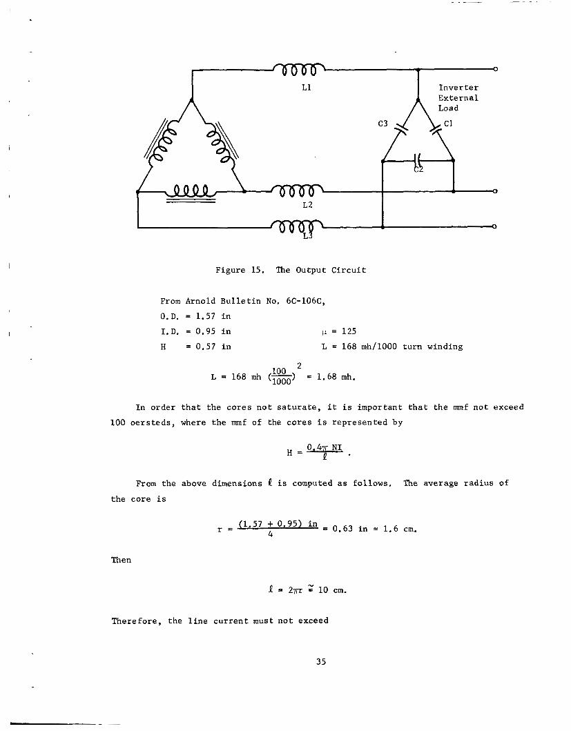
I n v e r t e r
1 L2 I 1 I 0
Figure 15. The Output C i r c u i t
From Arnold B u l l e t i n No. 6C-l06C,
O.D. = 1.57 i n
I . D . = 0.95 i n p = 125
H = 0.57 i n L = 168 mh/1000 tu rn winding
2 100 L = 168 mh (E) = 1.68 mh.
I n order t h a t the cores n o t s a t u r a t e , i t i s important t h a t t he mmf n o t exceed
100 oe r s t eds , where t h e mmf of the co res i s represented by
0 4 N I H = * I . From the above dimensions 1 i s computed as follows, The average r ad ius of
t h e co re is
Then
'v 1 = 277-r I: 10 cm.
Therefore , the l i n e c u r r e n t must n o t exceed
35
(100) (10) .-., I = = 8 amperes.
0.4T (100)
A t t he i n v e r t e r r a t e d load of 250 va t h e l i n e c u r r e n t s f o r a balanced r e s i s t i v e
load a r e
I = 250 va = 1.25 amps. x 115v
(2) Capacitors: C 1 , C 2 , C3; 400 v o l t s , 2pF + - 10% (Sprague 118P20594T4).
Peak vo l t age a c r o s s these c a p a c i t o r s i s
= J 2 x 115 vac = 163 v. 'peak
(3) The LC F i l t e r .
Inductors L1, L2, L3 and c a p a c i t o r s C 1 , C2, C3 connected a s i l l u s t r a t e d
i n Figure 15 form a three-phase f i l t e r which s e r v e s t o a t t e n u a t e the harmonics of
the 400 cps fundamental component contained i n the ou tpu t waveforms. This f i l t e r i n g
a c t i o n was discussed i n d e t a i l i n the Appendix o f Reference 1. For the balanced
c i r c u i t with L
r e s i s t i v e load the f i l t e r t r a n s f e r func t ion was shown t o be q u a d r a t i c with the
resonant frequency nominally
= L = L = L and C = C 2 = C3 = C wi th e i t h e r no load o r a balanced 1 2 3 1
The r e l a t i v e d i s t o r t i o n of t he nominal s tepped v o l t a g e waveform from the power
t ransformers was computed i n Reference 1 a s 15.25%. A t r a t e d balanced, r e s i s t i v e
load cond i t ions the f i l t e r was shown t o reduce the d i s t o r t i o n t o approximately 1.7%.
I n v e r t e r s p e c i f i c a t i o n s r e q u i r e t h a t t he r e l a t i v e d i s t o r t i o n be less than 5%. A t
these load cond i t ions the ou tpu t f i l t e r i s more than adequate. The f i l t e r ope ra t ion
a t o t h e r load cond i t ions inc lud ing r e a c t i v e loads and unbalanced loads i s c u r r e n t l y
being e x t e n s i v e l y i n v e s t i g a t e d by a computer program f o r handl ing t h e more com-
p l i c a t e d expressions.
The loads which the i n v e r t e r w i l l d r i v e are a n t i c i p a t e d t o be induc t ive . The
ou tpu t f i l t e r i s purposely designed as a c a p a c i t i v e o u t p u t impedance t o provide a
power f a c t o r c o r r e c t i o n when the i n v e r t e r i s d r i v i n g i n d u c t i v e loads. For example,
c a l c u l a t i o n s have shown t h a t f o r a r a t e d load of 250 v a wi th the c u r r e n t l e a d i n g
the vo l t age by 45 degrees the power f a c t o r of t he combined f i l t e r and load i s
36
approximately uni ty . Thus, a t these cond i t ions the i n v e r t e r ope ra t e s more e f f i -
c i e n t l y as a power source.
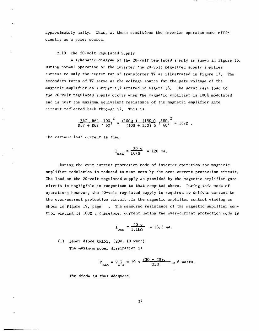
2.10 The 20-vol t Regulated Supply
A schematic diagram of the 20-volt r egu la t ed supply i s shown i n Figure 16.
During normal opera t ion of the i n v e r t e r the 20-volt r egu la t ed supply s u p p l i e s
c u r r e n t t o only the cen te r t a p of t ransformer T7 as i l l u s t r a t e d i n Figure 17. The
secondary t u r n s of T7 serve as the vo l t age source f o r the ga t e vo l t age of the
magnetic a m p l i f i e r as f u r t h e r i l l u s t r a t e d i n Figure 18. The worst-case load t o
the 20-vol t r egu la t ed supply occurs when the magnetic a m p l i f i e r i s 100% modulated
and i s j u s t the maximum equiva len t r e s i s t a n c e of the magnetic a m p l i f i e r ga t e
c i r c u i t r e f l e c t e d back through T7. This i s
L 100 150 (E) = 16752 . L R67 R69 100
R67 + R69 ( 60) = ( (1:0)+ :50)*: 60
The maximum load c u r r e n t i s then
- - - 2o = 120 ma. 'max 167Q
During the over -cur ren t p ro tec t ion mode of i n v e r t e r ope ra t ion t h e magnetic
a m p l i f i e r modulation i s reduced t o nea r ze ro by the over c u r r e n t p ro tec t ion c i r c u i t .
The load on the 20-volt r egu la t ed supply as provided by the magnetic ampl i f i e r ga t e
c i r c u i t i s n e g l i g i b l e i n comparison t o t h a t computed above. During t h i s mode of
o p e r a t i o n ; however, t he 20-volt regula ted supply i s requi red t o d e l i v e r c u r r e n t t o
t h e over -cur ren t p ro tec t ion c i r c u i t v i a the magnetic a m p l i f i e r c o n t r o l winding as
shown i n Figure 19, page . The measured r e s i s t a n c e of the magnetic ampl i f i e r con-
t r o l winding is l O O Q ; t he re fo re , c u r r e n t dur ing the over -cur ren t p ro tec t ion mode i s
1 =- 20 v ocp l.lkQ = 18.2 ma.
(1) Zener diode CR152, ( ~ O V , 10 w a t t )
The maximum power d i s s i p a t i o n i s
30 - 20)v 339 - 'U 6 watts. = V I = 2 o v ( 'max z z
The diode i s thus adequate,
37

- Load
-
Figure 16. The 20-volt Regulated Supply
(2) Res i s to r R72 (33R, 15 w a t t s d e r a t e d
The maximum power d i s s i p a t i o n i s
2 - ( 3 0 ~ - 2 0 ~ ) - 'ma, 33Q
t o 9 w a t t s a t 125OC)
- - 3 wa t t s .
Using the lower input vo l t age requirement of 25 vdc t o determine i f t he minimum
a v a i l a b l e c u r r e n t i s adequate t o supply t h e r e q u i r e d load c u r r e n t ,
120 ma < 152 ma.
(3) Capacitor C8 (47 I f , 35 v)
Some f i l t e r i n g i s r equ i r ed on t h e 20-vol t supply o u t p u t because o f t he
The v o l t a g e r a t i n g i s adequate and, p e r i o d i c (9.6kc) demand of t h e normal load.
from experimental obse rva t ions , the capac i t ance i s a l s o adequate.
2.11 Magnetic Amplifier Driver
A schematic o f t he magnetic a m p l i f i e r d r i v e r s t a g e i s shown i n Figure 17.
This c i r c u i t funct ions t o supply t h e g a t e e x c i t a t i o n r e q u i r e d f o r magnetic a m p l i f i e r
ope ra t ion .
38
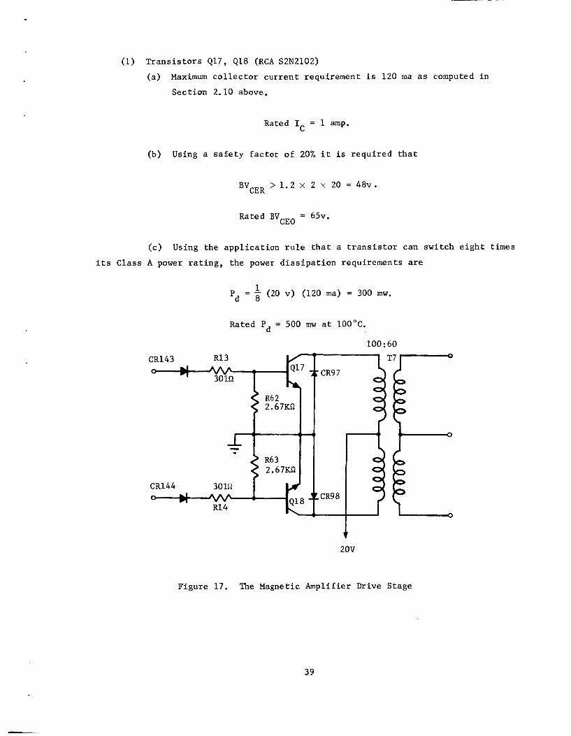
(1) T r a n s i s t o r s 417, 418 (RCA S2N2102)
(a) Maximum c o l l e c t o r cu r ren t requirement i s 120 m a as computed i n
Sec t ion 2.10 above.
Rated IC = 1 amp.
(b) Using a s a f e t y f ac to r o f 20% i t i s r equ i r ed t h a t
BVCER > 1 . 2 x 2 x 20 = 48v.
Rated BVCEO = 65v.
(c) Using the app l i ca t ion r u l e t h a t a t r a n s i s t o r can swi tch e i g h t times
i t s Class A power r a t i n g , the power d i s s i p a t i o n requirements are
1 Pd - - - (20 v) (120 m a ) = 300 mw.
t 20v
Figure 17. The Magnetic Amplif ier Drive Stage
39
(d) Using t h e same argument f o r frequency requirements
Sec t ion 2.7, t he r equ i r ed f i s 0
f0 = 10 x 4.8 kc = 48 kc.
Rated f = 60 mcs. a:
Since f = f 1100, t h e frequency requirements a r e adequately B a r
a s p re sen ted i n
m e t .
(e) The base c u r r e n t r equ i r ed t o s a t u r a t e the 2N2102 f o r t h e 120 m a
c o l l e c t o r c u r r e n t i s
(i)
( i i ) IB = 4 ma (from l a b o r a t o r y measured c o l l e c t o r C h a r a c t e r i s t i c s ) .
IB = 5 ma a t 100°C (manufacturer ' s t y p i c a l c o l l e c t o r c h a r a c t e r i s t i c s ) .
The base of t r a n s i s t o r s 417 and 418 are d r iven by an SN511A u n i t i n t h e frequency
countdown c i r c u i t . Using the manufacturer ' s SN511A ou tpu t c h a r a c t e r i s t i c s as shown
i n Figure 8, page , and assuming 0.7 v o l t s f o r t he forward drop of t he diodes and
t h e t r a n s i s t o r base emitter junc t ion the a c t u a l base c u r r e n t i s e s t ima ted as f 01 lows.
4 0 3 - 'R13 :301 -+ ,bo,' Q
= 5.8 ma, and - -
IB = 6 ma - = 5.54 ma. 2.67 KR
Based on the manufacturer ' s publ ished c h a r a c t e r i s t i c s t he base c u r r e n t as computed
above i s marginal. However, t h e measured c h a r a c t e r i s t i c s a t high temperature show
t h e t r a n s i s t o r s t o have higher ga ins than claimed by the manufacturer and the
a v a i l a b l e c u r r e n t t o be adequate. From manufac tu re r ' s c h a r a c t e r i s t i c curves , a
base c u r r e n t a s low as 4 ma can be t o l e r a t e d wi thou t any s i g n i f i c a n t i n c r e a s e i n
VCE above V
higher ga ins than t h e minimum claimed by the manufacturer , and it i s probable t h a t
t h i s i s done through the S-type s p e c i f i c a t i o n .
These t r a n s i s t o r s should be screened t o i n s u r e t h a t they have CE sat'
(2) Diodes CR143, CR144 (1N645 - 400 v PIV, 150 m a a t 150°C).
These diodes are more than adequate f o r t h e c u r r e n t s computed i n (1) above.
R e s i s t o r s R13, R14, R62, R63 (1/4 watt d e r a t e d t o 1/10 w a t t a t 125'C).
The maximum power d i s s i p a t e d by any of t h e s e r e s i s t o r s i s (3 )
1 2 'v 62 mw < 10 w a t t .
'd < 301c1 -
40
(4) Diodes CR97, CR98 (1N645, 400 v PIV, 150 m a a t 15OoC)
The c u r r e n t conducted by these diodes w i l l be less than t h e 120 m a
maximum c o l l e c t o r c u r r e n t computed f o r t he t r a n s i s t o r ; t h e r e f o r e , t h e diodes a r e
adequate.
(5) Transformer T7
For t h e t ransformer a p p l i c a t i o n it i s r e q u i r e d t h a t
where E = 30 v o l t s ,
AT = 1/4.8kc = 0.2083 msec,
N = 100 tu rns , and
Afe i s unknown f o r t he computation above ; however, experimental obse rva t ions r e v e a l
t h a t t he t ransformer i s adequate fo r the intended funct ion.
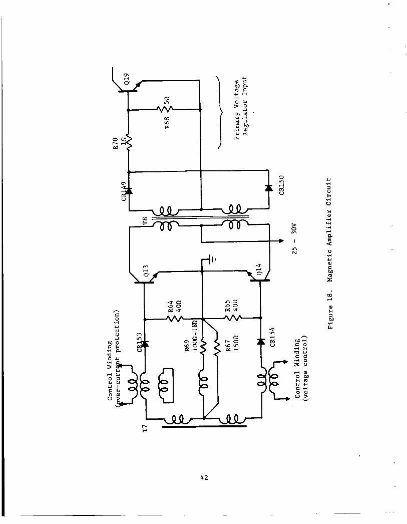
2.12 Magnetic Amplifier C i r c u i t
A schematic diagram of the magnetic a m p l i f i e r c i r c u i t i s shown i n
F igu re 18. The ope ra t ion of t he c i r c u i t i s desc r ibed i n d e t a i l i n Reference 1.
(1) T r a n s i s t o r s 413, 414 (2N2034A)
(a) The maximum c o l l e c t o r c u r r e n t requirement i s e s t ima ted as follows.
Assuming 0 . 6 ~ f o r each of t he forward drops i n diodes CR149 and CR150 and t r a n s i s t o r
Q19 base t o emitter junc t ion , t he maximum ou tpu t c u r r e n t t o the primary vo l t age
r e g u l a t o r i s
1 3 ~OV(-) - 1 . 2 ~ - - 100 = 2.7 amp. Imax In
The corresponding c o l l e c t o r cu r ren t i n 413 and 414 i s
I C = 2.7 amp x - l3 ‘v 350 ma. 100 -
Rated I C = 3 amps.
41
(!,- c: I rn
f% U .r(
. - .I4 W k PI
0 G M
2 co l-l
A
42
(b) Assuming a s a f e t y f a c t o r of 20%,
Required BV
Rated BVCEO = 70v, and
Rated BVCES = 80v.
= 2 x 30 x 1.2 = 72v, CER
The comparison above appears unsa t i s f ac to ry . The fol lowing cons ide ra t ions
i s a worst-case r a t i n g f o r the BVCEO favorably modify the conclusion o f (b).
a p p l i c a t i o n considered here. The a c t u a l parameter of i n t e r e s t is BV f o r an
emi t te r -base r e s i s t a n c e of 40 ohms. BVCER w i l l be g r e a t e r than BVCEO and l e s s
than BVCES.
a f a c t o r f r equen t ly used t o provide f o r switching t r a n s i e n t s i n s a t u r a t i n g o s c i l l a t o r
c i r c u i t s . Some s a f e t y f a c t o r is des i r ab le , b u t 20% i s probably excess ive s ince t h i s
i s n o t a s a t u r a t i n g app l i ca t ion . It i s concluded t h a t t he t r a n s i s t o r s have an
adequate vo l t age r a t i n g .
CER
Also, the 20% s a f e t y f ac to r used i n determining the r equ i r ed BV i s CEO
(c ) Using the app l i ca t ion r u l e t h a t a t r a n s i s t o r can switch e i g h t times
i t s Class A power r a t i n g , t he power d i s s i p a t i o n requirements are
2 - - - 1 3 Ov = 1.9 wat ts
'd 8 10; 2 k la (77)
Rated Pd = 5 wat ts , Tc = 100°C
= 0.3 watts, T = 100°C A
The comparison i n (c) i s a l s o unfavorable , and a thermal a n a l y s i s o f the
:completed system i s requi red t o estimate the a c t u a l thermal ope ra t ing po in t of the
t r a n s i s t o r .
s i s t o r w i l l be made i n subsequent analyses .
however, it must be concluded t h a t the t r a n s i s t o r power r a t i n g i s inadequate. The
des ign should be j u s t i f i e d on some o t h e r b a s i s , e.g. , an experimental study.
A more r igo rous es t imate o f the power d i s s i p a t i o n r equ i r ed o f the t r an -
On the b a s i s of t he above a n a l y s i s ,
A t h igh ambient temperatures , 413 and 414 have been observed t o c o n s i s t e n t l y
f a i l through "thermal run-away'' as t h e average c u r r e n t through t h e t r a n s i s t o r s
approaches a maximum, i.e., t h e magnetic ampl i f i e r approaches 100% modulation. This
r e f l e c t s the inadequate power r a t i n g a t h igh temperatures. A subsequent s ec t ion of
t h i s memorandum w i l l d i s cuss t h i s observed f a i l u r e mode.
(d) Using the same argument f o r frequency requirements as presented i n
Sec t ion 2.7,
4 3

Required = 10 x 4.8 kc = 48 kc. 5 Rated fr = 1 mc minimum,
and the frequency requirements a r e m e t .
( e ) The base d r i v e requirement f o r 413 and 414 as determined from the
manufacturers ' da t a b u l l e t i n i s
IB < 10 ma.
The base d r i v e c u r r e n t i s e s t ima ted from an a n a l y s i s o f Figure 18 as f o l h w s .
The t o t a l r e s i s t a n c e i n the base c i r c u i t during magnetic a m p l i f i e r s a t u r a t i o n i s
% < 15052 + l O O R + 1 . 3 R 2 250R.
An estimate of base c u r r e n t is then determined as
(12 - 1 . 5 ) ~ 0.8 v ~ 22 ma, 'B > 25052 40 R
It i s a l s o r equ i r ed t h a t the base d r i v e c u r r e n t be n e g l i g i b l e p r i o r t o t h e
magnetic a m p l i f i e r "turn-on" t i m e . A s a f i r s t approximation, t he "off-time" base
c u r r e n t i s l imi t ed t o the magnetizing c u r r e n t i n the g a t e winding of t he magnetic
ampl i f i e r .
amperes, o r mag N 25 0
I < 1 .4 ma. B
From .the manufacturer ' s da t a i t i s e s t a b l i s h e d t h a t t h e t r a n s i s t o r conduction
f o r t h i s base cu r ren t is n e g l i g i b l e .
(2) Diodes CR153, CR154 [1N3730]
From manufacturer 's r a t i n g s , a t 100°C
I f / V f = 750 ma/.9v
PIV = 100 v o l t s .
4 4
These c h a r a c t e r i s t i c s a r e more than adequate .
(3) R e s i s t o r s [minimum power r a t i n g i s 3 w a t t s ]
The maximum power d i s s i p a t e d by any r e s i s t o r i s
-@d = 1 .8 watts < 3 w a t t s . 2 x 40 Pd <<
2.13 Voltage E r r o r Detection C i r c u i t
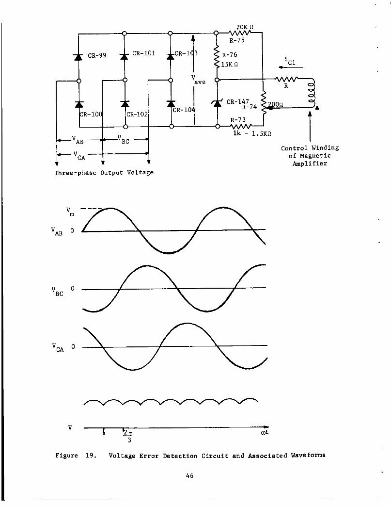
A schematic o f t h e vo l t age e r r o r d e t e c t i o n c i r c u i t i s presented i n
F igu re 19. The three-phase vo l t age d e t e c t i o n process y i e l d s t h e r i p p l e dc v o l t a g e
a t t h e bottom of t h e f i g u r e . The average va lue o f t h e dc is computed by
3 2T
3
Vave = 3vm s i n x dx = - - 7J "In
and, f o r t h e nominal ou tpu t i n v e r t e r v o l t a g e of 115 vac rms V becomes ave
(1) R e s i s t o r s R73 [3 w a t t s ]
Assuming t h a t R74 i s s e t a t i t s midpoint, t h e r e s i s t o r c u r r e n t s i n d i c a t e d
i n F igu re 19 can be e s t ima ted from t h e loop v o l t a g e equat ions a s fol lows:
20100il + 1200(i l - i2) = 156, and
100 i2 + 1200(i2 - il) = -8 .4
which y i e l d
i = 7.3 m a , and 1
i = - 0.31 m a . 2
The power d i s s i p a t i o n i n R73 is
2 p = (7.3 ma + 0.3 ma) (1.1161) = 63.5 mw. d
45
Three-phase Output Voltage
V -L
A V!h cut 3
Figure 1 9 . Voltage Error Detection Circuit and Associated Waveforms
46
(2) Res i s to r R75 [5 wa t t ]
Using t h e c u r r e n t s computed i n (1) above, t h e power d i s s i p a t i o n i n R75 i s
P = ( 7 . 3 ma)2 (20KQ) = 1.07 w a t t . d
(3) Potent iometer R74 [1.5 wat t ]
Assuming a wors t -case condi t ion when i = 0, t h e maximum power d i s - 2 s i p a t e d i n R74 i s
Pd = (7.3 mal2 (200 ohms) = 11 mw.
(4) Res i s to r R76 [5 wa t t ]
The power d i s s i p a t i o n i n R76 is
(5) Zener diode CR147[VZ = 8 . 4 ~ 1
The power d i s s i p a t i o n i s
(156 - * + 0.3 m a ] = 86.5 m. Pd = 8.4 v [ 15KR
(6) Diodes CR99 - CR104 [1N645]
Since t h e diodes sha re the cu r ren t , t h e average cu r ren t i n any diode is
156 3 F= 6 m a . 1 Iave 7 [
(15 x 20)KR2 3 5Kfl
The r a t e d average cu r ren t i s 250 ma @ 100°C; t h e r e f o r e , t h e diodes a r e adequate.
2.14 Over-current P ro tec t ion C i r c u i t
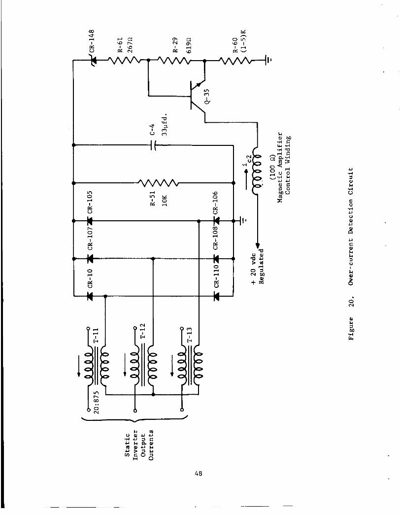
A schematic diagram of the over -cur ren t d e t e c t i o n c i r c u i t i s presented
i n F igure 20. This c i r c u i t func t ions t o d e t e c t high output c u r r e n t s t h a t may
p o t e n t i a l l y damage t h e i n v e r t e r and provides a con t ro l s i g n a l t o t h e magnetic
a m p l i f i e r t o reduce t h e i n v e r t e r o u t p u t .
t ransformers T 1 1 , T12 and T13 t h e primary windings o f which a r e loca ted i n the
i n v e r t e r ou tput buses .
The output cu r ren t s are sensed by
Through the t ransformer t u r n s r a t i o the low vo l t age drop
47
a w I
i vr 0 rl
u A
d d
b
U .d 7 u k
.I4 u C 0 .!-I . . u u Q) U
k k 2 c) I k
d .
0 N
48
ac ross t h e p r i m a r y winding (which i s p ropor t iona l t o t h e l i n e cu r ren t ) is s tepped
up t o a high vo l t age which is r e c t i f i e d i n t h e three-phase r e c t i f i e r c i r c u i t . The
impedance of t he primaries of these t ransformers is very low, a s shown i n (2)
below, and n e g l i g i b l e i n comparison t o t h e output f i l t e r chokes L 1 , L2 and L3;
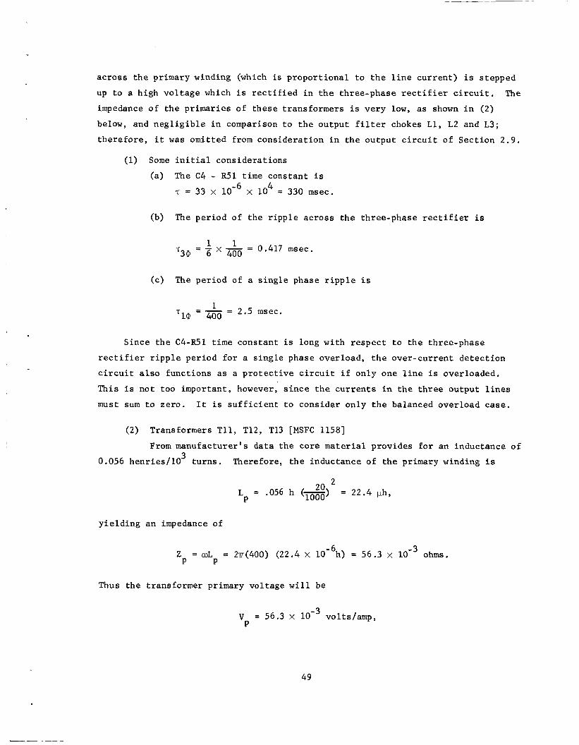
t he re fo re , i t was omit ted from cons idera t ion i n the output c i r c u i t of Sec t ion 2 . 9 .
(1) Some i n i t i a l cons idera t ions
(a) The C4 - FS1 time constant i s
z = 33 x x lo4 = 330 msec.
(b) The per iod o f t he r i p p l e ac ross t h e three-phase r e c t i f i e r is
1 1 x - = 0.417 msec. ‘30 = 400
(c) The per iod of a s i n g l e phase r i p p l e i s
= - = 2.5 msec. ‘10 400
Since t h e C4-R51 time cons tan t is long wi th r e spec t t o t h e three-phase
r e c t i f i e r r i p p l e per iod f o r a s i n g l e phase overload, t h e over -cur ren t de t ec t ion
c i r c u i t a l s o func t ions a s a p r o t e c t i v e c i r c u i t i f on ly one l i n e i s overloaded.
This i s not too important , however, s i n c e t h e c u r r e n t s i n t h e t h r e e output l i n e s
mus t sum t o zero . It i s s u f f i c i e n t t o cons ider on ly t h e balanced overload case .
(2) Transformers T11, T12, T13 [MSFC 11581
From manufacturer‘s data the core m a t e r i a l provides f o r an inductance of n
0.056 henries/103 t u r n s . Therefore, t h e inductance of t h e primary winding i s
20 L = .056 h (-) = 22.4 ph, P 1000
y i e l d i n g an impedance of
-6 Z = OL = 2n(400) (22.4 x 10 h) = 56.3 x ohms.
P P
Thus the t ransformer primary vol tage w i l l be
V = 56.3 x volts/amp, P
49

and t h e t ransformer secondary vo l t age w i l l be
-3 875 20
Vs = (56.3 x 10 ) (-) = 2.46 volts/amp of l i n e c u r r e n t .
(3) Three-phase r e c t i f i e r
The three-phase r e c t i f i e r output vo l t age i s equal t o t h e maximum
ins tan taneous d i f f e rence between the maximum and minimum inpu t v o l t a g e s . The
ind iv idua l i npu t vo l t ages from t h e secondary windings of T 1 1 , T12 and T13 have
the same phase r e l a t ionsh ip as the t h r e e vo l t age waveforms i n F igure 19.
maximum ins tan taneous vo l t age d i f f e r e n c e can be obta ined by cons ider ing the
vo l t age i n t h e i n t e r v a l
The
Tl < ut < 5, o r
2 n voCp = 4 2 vS [ s i n u t - sin(cot - TI].
The maximum occurs when * = 0, o r d t
cos cot - cos ( u t - 3) 2Tl = 0
which is only t r u e a t ut = ~ / 3 . Therefore ,
n- Tl v = & v s [ s i n ? - s i n ( - 711 O C P
7T Ti = d2 v s i n
S
= d 2 (2.46 volt/amp) s i n $ = 6.05 vdc/rms amp of l i n e c u r r e n t .
Experimental ly , the output l i n e c u r r e n t s have never been observed t o exceed
Accepting t h i s as a worst-case va lue , t h e maximum three-phase r e c t i f i e r ou tput
vo l t age is
2 amps.
V = (6.05 v/amp) ( 2 amp) = 12.10 v . OCP
(4) Zener diode CR148
Since CR148 is an 8 .4 v o l t zener , t h e th re sho ld l i n e c u r r e n t va lue f o r
[1N3156AY Vz = 8.4 v , 400 mw.]
t he over -cur ren t de t ec t ion c i r c u i t is
50
8.4 v 6.05 v/amp I = = 1.39 r m s amp of l i n e c u r r e n t .
The observed va lue o f th reshold cu r ren t i s 1 . 4 amps.
The m a x i m u m cu r ren t through CR-148 is
and t h e maximum power d i s s i p a t i o n is
Pd = VzIz = ( 8 . 4 ~ ) (2.92 ma) = 24.5 mw.
The power and cu r ren t r a t i n g s a r e more than adequate , 1 1
10 (5) Res i s to r s R29, R60, R61 [z w a t t , &rates t o - wat t1
The maximum power d i s s ipa t ed i n e i t h e r o f these r e s i s t o r s i s determined
by computing f o r R60
pd = (2.92 ma)' (5KR) = 43 mw.
1 4 Thus t h e - w a t t r a t i n g f o r a l l r e s i s t o r s i s adequate .
1 1 10 (6) Res i s to r R51[ T w a t t , de ra t e s t o - w a t t ]
Using t h e maximum r e c t i f i e r ou tput v o l t a g e of 12.10 v, t h e power
d i s s i p a t i o n i s
2 (l2*l0 = 14.6 P = d 1 OKn
(7) Capaci tor C4 [35 V ~ C ]
For t h e maximum r e c t i f i e r ou tput vo l t age of 12.10 t h e vo l t age r a t i n g is
adequate .
From t h e i n i t i a l cons idera t ion i n (1) above, t h e capac i tance is adequate.
(8) Diodes CR105 - C R l l O [1N645]
The maximum average cu r ren t conducted by any diode i s one - th i rd t h e
t o t a l ou tput cu r ren t from t h e br idge o r
12'10v + 2.92 ma) = 1 . 4 ma. I ave = 5
Rated Iave = 150 ma a t 150°C.
51

(9) T r a n s i s t o r , 435 [2N718A]
(a) The maximum c o l l e c t o r c u r r e n t requirement was computed i n s e c t i o n
2.10 t o be 18.2 ma.
Rated IC = 150 ma .
Required BVm0 = 20 v o l t s . (b)
Rated BVCEO = 32 v o l t s .
The maximum p o s s i b l e power d i s s i p a t i o n i s ( c )
Pd = (18.2 m a ) (20 v o l t s ) = 364 mw.
Rated d i s s i p a t i o n a t a c a s e temperature of 100°C is
Pd = 1 .0 w a t t .
2.15 Primary Voltage Regulator
A schematic diagram o f t h e primary v o l t a g e r e g u l a t o r is shown i n F i g u r e 2 1 .
The ou tpu t o f t h e magnetic a m p l i f i e r c i r c u i t is supp l i ed as base d r i v e t o t h e
p a r a l l e l t r a n s i s t o r switches Q19, 420 and 421 which s h a r e t h e high c u r r e n t r equ i r ed
by t h e ou tpu t conve r t e r s .
(1) Inpu t f i l t e r
The input f i l t e r is composed of choke L4 and c a p a c i t o r C5 and serves t h e primary purpose o f i s o l a t i n g t h e inpu t primary v o l t a g e bus from c u r r e n t t r a n -
s i e n t s induced by t h e heavy c u r r e n t switching a t t h e 9.6 kc ra te . Formal
s p e c i f i c a t i o n s f o r t h e i n v e r t e r i nc lude no requirements p e r t a i n i n g t o t h e amount
o f f i l t e r i n g t o be included; however, it is obvious t h a t some f i l t e r i n g is necessary t o i s o l a t e t h e input bus from t h e 9.6 kcps.
(a) Inductor L4
Core Data; MoPerm B-070127-3 (Arnold Eng .)
p = 125
OD = 1.3 i n
I D = 0.785 i n
h = 0.420 i n (height)
A f e = 0,666 cmL
1 = 8.3 cm(mean magnetic path) L = 127 &/lo3 t u r n s
52

& Q) U rl .rl Fr,
a C (d
& 0 U (d rl 1 M
53
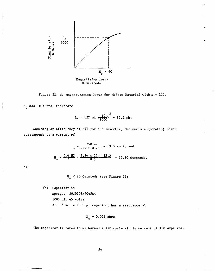
H = 90 5
Magnetizing force H- Oe r s t e d s
Figure 22. dc Magnet izat ion Curve f o r MoPerm Material w i t h p = 125.
L has 16 tu rns , t h e r e f o r e 4
2 L4 = 127 mh (-) 16 = 32.5 bh. 1000
Assuming an e f f i c i e n c y of 75% f o r t h e inve r t e r , . t h e maximum ope ra t ing po in t
corresponds to a cu r ren t of
I = 250 va = 13.3 amps, and o 25v x 0.75
0 * 4 N1 1'26 l6 13'3 = 32.10 Oersteds, 0 =7= 8.3
or
H < 90 Oers teds ( see F igu re 22) 0
(b) Capaci tor C5
S Prague 202D108X9045A4
1000 p f , 45 v o l t s
A t 9.6 kc, a 1000 pf c a p a c i t o r has a r eac t ance of
Xc = 0.065 ohms.
The capac i to r is r a t e d t o wi ths t and a 120 c y c l e r i p p l e c u r r e n t of 1.8 amps r m s .
54
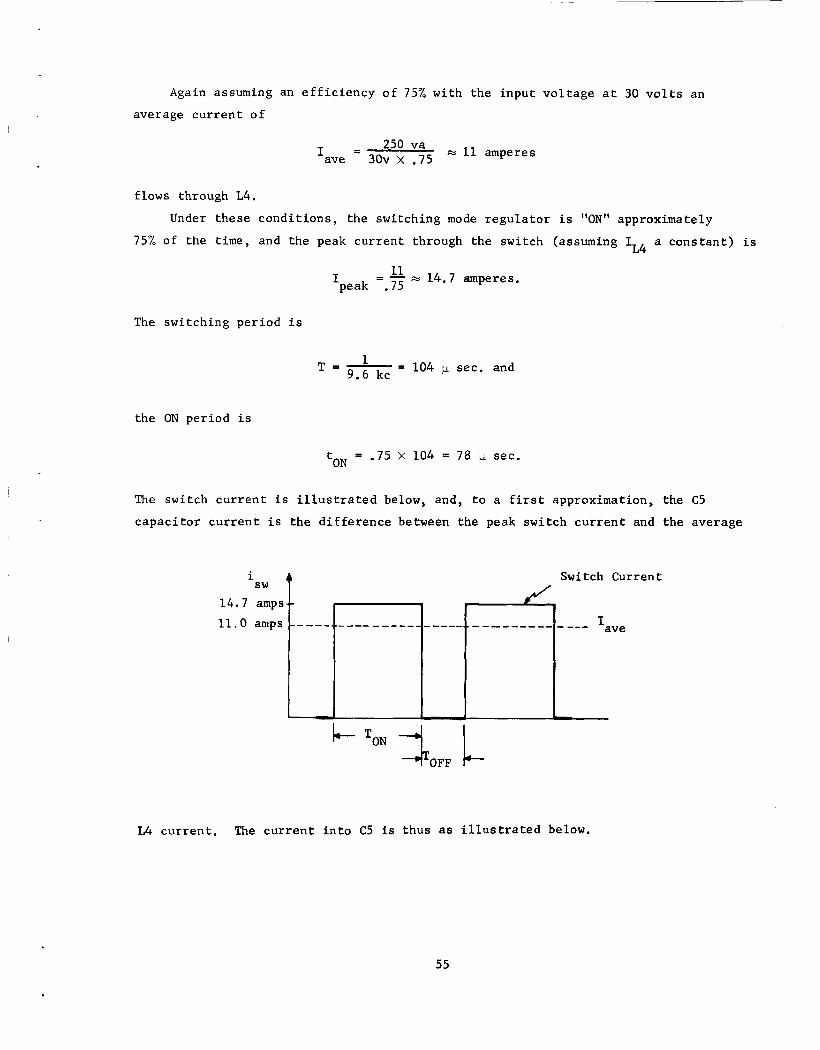
Again assuming
average c u r r e n t o f
an e f f i c i e n c y o f 75% wi th the i n p u t vo l t age a t 30 v o l t s an
= 250 va = 11 amperes 'ave 30v x .75
flows through L4.
Under these cond i t ions , t he switching mode r e g u l a t o r i s "ON" approximately
75% of the t i m e , and the peak cu r ren t through the switch (assuming I a cons t an t ) i s L4
11 'peak .75
- - - n. 14.7 amperes.
The swi tch ing per iod i s
104 p sec. and 1 9.6 kc
T=-=
the ON per iod i s
tON = .75 x 104 = 78 sec.
The switch c u r r e n t i s i l l u s t r a t e d below, and, t o a f i r s t approximation, the C5
c a p a c i t o r c u r r e n t i s the d i f f e r e n c e between the peak swi tch c u r r e n t and the average
L4 cu r ren t . The c u r r e n t i n t o C 5 i s thus as i l l u s t r a t e d below.
55

c5 I i
Consequently, t h e r m s r i p p l e c u r r e n t i n C5 i s
2 2 1 / 2 [ (3.7 amp) x 78 psec + (11 amp) x 26 psec] 1 - - ' r m s 104 u sec
= 6 . 4 amps.
This e s t ima te o f r m s r i p p l e c u r r e n t i n C5 is p e s s i m i s t i c , p r i n c i p a l l y because
of t h e assumption of constant c u r r e n t i n L 4 . It does i n d i c a t e , however, t h a t t h e
r i p p l e c u r r e n t i n C5 i s cons ide rab ly more than t h e 1 .8 amperes considered s a f e by
t h e manufacturer. It seems a d v i s a b l e t o r e p l a c e C5 wi th a s i m i l a r c a p a c i t o r i n a
d i f f e r e n t ca se t h a t has a h ighe r r i p p l e c u r r e n t r a t i n g . Such c a p a c i t o r s a r e
a v a i l a b l e i n t h e same Sprague type.
The measured r m s r i p p l e c u r r e n t i n C5 i s 5 .3 amps. The r i p p l e c u r r e n t i s n o t
independent of t h e source v o l t a g e c h a r a c t e r i s t i c s , however.
I f L4 has a constant c u r r e n t of 11 amperes, t h e v o l t a g e a c r o s s C5 w i l l i n c r e a s e
above V by i n
1 C V = - J i d t
6 =- (11) (104 x 10- )
= 0.286 v o l t s .
This i s a n e g l i g i b l e r ise and i l l u s t r a t e s t h a t C 5 can be cons ide rab ly reduced.
p r i n c i p l e mode of f a i l u r e recognized f o r e l e c t r o l y t i c c a p a c i t o r s i s s h o r t i n g , and
furthermore, i t i s known empi r i ca l ly t h a t t h e p r o b a b i l i t y o f f a i l u r e of c a p a c i t o r s
The
56

1 -
is propor t iona l t o t h e capac i tance . Therefore , p o t e n t i a l l y a s i g n i f i c a n t con t r ibu t ion
can be r e a l i z e d by reducing the capac i tance of C 5 .
of r i p p l e cu r ren t cons idera t ions , however.
This cannot be done independently
The input f i l t e r a t t e n u a t e s f requencies above
n. 900 cps 1 f = r 27rJLC
a t about 1 2 db loc t .
(2) The Output F i l t e r
The output f i l t e r smooths t h e pulse-width modulated inpu t vo l t age t o a
near dc p o t e n t i a l on t h e c o n t r o l l e d dc bus ( r egu la to r o u t p u t ) .
of t h i s r e p o r t w i l l d i scuss t h e con t ro l l ed dc bus i n more d e t a i l .
A fol lowing sec t ion
(a) Inductor ; L5
Core Data; MoPerm D-082168-3 (Arnold Engr .)
p = 125
OD = 1.57 i n
I D = 0.950 i n
h = 0.570 i n (he ight ) 2 = 1.06 cm A f e
1 = 10.1 cm (mean magnetic path)
L = 168 mh/103 t u r n s
L5 has 37 t u r n s , t he re fo re
3 1 L5 = 168 (-) mh = 230 ph. 1000
Assuming an i n v e r t e r e f f i c i e n c y of 75%, t h e maximum ope ra t ing poin t i s est imated
as follows.
- - 250 va = 16.7 amps, and I o 20v x .75
0.4 M 1.26 x 37 x 16.7 = 7 2 Oersteds, 0 =P= 10.11
o r
H, < 90 Oersteds (see F igure 22) .
A c r i t i c a l cons ide ra t ion €or L5 is t h a t t he inductor no t "bottom", i . e . , H
become zero , a t minimum loads . If L5 does bottom t h e output f i l t e r w i l l cease t o
be an averaging f i l t e r and high induct ive t r a n s i e n t s could appear a c r o s s CR151.
57
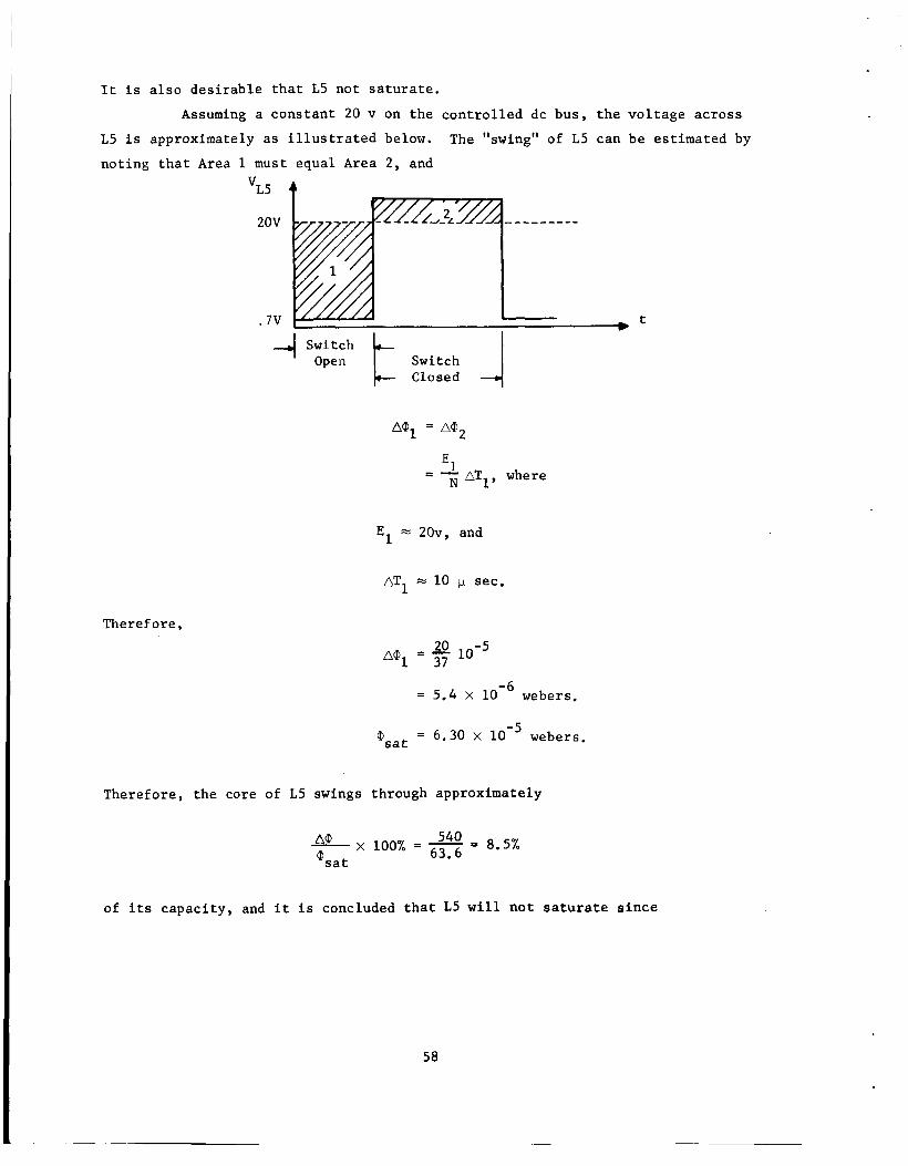
It i s a l s o d e s i r a b l e t h a t L5 not s a t u r a t e .
Assuming a cons tan t 20 v on t h e c o n t r o l l e d dc bus, t h e vo l t age ac ross
L5 i s approximately as i l l u s t r a t e d below.
not ing t h a t Area 1 must equal Area 2 , and
The "swing" of L5 can be es t imated by
vL5
20v
. JV
4
t
= 7 AT1, where
El = 20v, and
AT1 = 10 p sec.
Therefore ,
= 5.4 x 10 -6 webers.
= 6 . 3 0 X webers. @ s a t
Therefore , t he core of L5 swings through approximately
of i t s capac i ty , and i t i s concluded t h a t L5 w i l l no t s a t u r a t e s i n c e
58

7 2 Oersteds + (.085) (90) Oersteds < 90 Oersteds.
From t h e manufacturer ' s dc magnet izat ion curve, i t i s es t imated t h a t t h e
core would not bottom i f t h e minimum ope ra t ing po in t w a s such t h a t
> 10 Oers teds . Hmin
This corresponds t o a minimum curren t of
lo = 2.6 amp, I = 37 x 1.26
At zero ex te rna l load , L5 has been observed t o bottom. The t r a n s i e n t s observed,
however, a r e i n s i g n i f i c a n t .
(b) Capaci tors C6, C7
Sprague 202D108x9045A4
1000 pf , 45 v .
I f i t is assumed t h a t t h e cur ren t i n L5 is a cons t an t , then the r i p p l e cu r ren t
i n C
be some r i p p l e on t h e c o n t r o l l e d dc bus and some r i p p l e c u r r e n t through C
t h e cu r ren t i n L 5 i s not a cons tan t and C a l s o se rves t o s t o r e energy re turned t o
t h e con t ro l l ed dc bus by t h e power converter s t a g e s .
r i p p l e cu r ren t i n C is
(Co i s the p a r a l l e l combination o f C6 and C7) w i l l be nea r zero . There w i l l
s i n c e 0
0
0
The wors t -case measured
0
= 2.2 amperes. Irms
S ince C6 and C7 are each r a t e d f o r 1 .8 amperes of r m s r i p p l e c u r r e n t , t h i s f i l t e r
is considered s a f e .
The output f i l t e r a t t e n u a t e s f requencies above i t s 230 cps resonant frequency
a t 1 2 db/oc t .
(3) Diode CR151 (HF3C)
CR151 is requi red t o be a f a s t recovery diode t h a t provides a path of
c u r r e n t flow through L5 when t h e t r a n s i s t o r r e g u l a t o r switch is opened. It must
block approximately 30 v o l t s , and car ry an average cu r ren t of approximately 4
amperes. No da ta i s c u r r e n t l y a v a i l a b l e d e s c r i p t i v e of t h e HF3C.
(4) Regulator switch 419, 420, 421
The r e g u l a t o r switch cons i s t of t h r e e p a r a l l e l e d 2N1937 t r a n s i s t o r s .
59

(a) The switch, i n an OFF mode, must block 30 v o l t s . Therefore;
Required BV = 30 v o l t s CEO
Rated BVCEO = 80 v o l t s
(b) Assuming 75% e f f i c i e n c y , t h e maximum average cu r ren t t h e switch is
r equ i r ed t o conduct is
250 va = 13.5 amps. - - I c ave 25v x .75
The measured average cu r ren t a t r a t e d load and an input vo l t age of 25 v o l t s is
approximately 14 amps. Assuming the switch i s ON 75% of t h e per iod a t f u l l load,
t he peak cu r ren t i s
- - = 13'5 18 amps. - IC peak .75
Each t r a n s i s t o r has a r a t e d cu r ren t of I = 20 amps, continuous a t 25'C. C
(c) Power d i s s i p a t i o n :
I f case temperature does not exceed 100°C and switching on a
r e s i s t i v e load l i n e is assumed, a s i n g l e 2N1937 w i l l always be f a r i n s i d e a safe,
continuous opera t ing reg ion .
and a thorough ana lys i s of power d i s s i p a t i o n r e q u i r e s cons ide ra t ion of mounting and
hea t s i n k condi t ions . Assuming an e f f i c i e n c y of 70%, t h e switch i s r equ i r ed t o
c o n t r o l
Some de ra t ing i s r equ i r ed f o r h igher case temperatures ,
250 v a l . 7 = 360 w a t t s .
I f t he 2N1937 can cont inuously d i s s i p a t e
a s i n g l e t r a n s i s t o r could be considered f o r t h e swi tch .
Rated Pd = 150 watts a t Tc = 100°C.
I n an overload condi t ion , t h e switch can be r equ i r ed t o conduct more than 20
amperes average and has been observed i n t h e l abora to ry t o conduct approximately
24 amperes average, From (c) above, two 2N1937 t r a n s i s t o r s a r e r equ i r ed t o perform
t h e switching funct ion, and two a r e adequate from power d i s s i p a t i o n cons ide ra t ions .
60
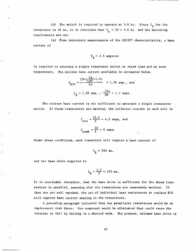
I
(d) The switch i s requi red t o ope ra t e a t 9 .6 kc. S ince f f o r t he
t r a n s i s t o r i s 18 m c , i t i s concluded t h a t f > 10 x 9.6 kc and t h e switching B
requirements a r e met.
T
(e ) From l abora to ry measurements o f t he 2N1937 c h a r a c t e r i s t i c s , a base
cu r ren t of
IB = 2.5 amperes
is r equ i r ed t o s a t u r a t e a s i n g l e t r a n s i s t o r switch a t r a t e d load and a t room
temperature . The minimum base cur ren t a v a i l a b l e is es t imated below,
13 2 5v (-1 - 1 . h 100 = 1.85 amp., and 'R70 1Cl
IB = 1.85 a m p , - = 1 . 7 amps.
The minimum base cu r ren t is not s u f f i c i e n t t o s a t u r a t e a s i n g l e t r a n s i s t o r
swi tch . I f t h r e e t r a n s i s t o r s a r e matched, t h e c o l l e c t o r c u r r e n t i n each w i l l be
= - - 13*5 - 4.5 amps, and Iave 3
18 = - = 6 amps. 'peak 3
Under these condi t ions , each t r a n s i s t o r w i l l r e q u i r e a base c u r r e n t of
IB = 300 m a ,
and t h e base d r i v e suppl ied i s
1 = A - ' - 570 m a . B 3
It i s concluded, t he re fo re , t h a t the base d r i v e i s s u f f i c i e n t f o r t h e t h r e e t r an -
s i s t o r s i n p a r a l l e l , assuming t h a t t h e t r a n s i s t o r s a r e reasonably matched. I f
they a r e not w e l l matched, t he use of i nd iv idua l base r e s i s t a n c e s t o r ep lace R70
w i l l improve base cu r ren t shar ing i n t h e t r a n s i s t o r s .
A preceding paragraph indica ted t h a t two p a r a l l e l e d t r a n s i s t o r s would be an
improvement over t h r e e .
i n v e r t e r t o f a i l by f a i l i n g i n a shor ted mode. The p resen t , minimum base d r i v e i s
One component would be e l imina ted t h a t could cause the
61
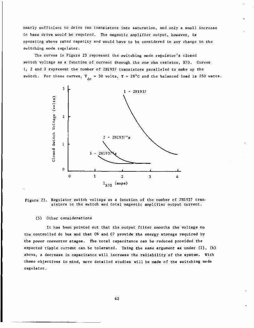
n e a r l y s u f f i c i e n t t o d r i v e two t r a n s i s t o r s i n t o s a t u r a t i o n , and on ly a s m a l l i n c r e a s e
i n base d r i v e would be r equ i r ed . The magnetic a m p l i f i e r ou tpu t , however, is
ope ra t ing above r a t e d capac i ty and would have t o be considered i n any change i n t h e
switching mode r e g u l a t o r .
The curves i n F igu re 23 r ep resen t t h e switching m d e r e g u l a t o r ' s c losed
switch v o l t a g e a s a func t ion of c u r r e n t through t h e one ohm r e s i s t o r , R70. Curves
1, 2 and 3 r ep resen t t h e number o f 2N1937 t r a n s i s t o r s p a r a l l e l e d t o make up t h e
swi t ch . For these curves, V = 30 v o l t s , T = 28OC and t h e balanced load i s 250 watts. dc
n a U rl 0 >
al M m U d 0 > I: V U .rl 3 m '0 al (I) 0 rl CJ
v
Figure 23. Regulator switch v o l t a g e a s a func t ion o f t h e number of 2N1937 t r a n - s i s t o r s i n t h e switch and t o t a l magnetic a m p l i f i e r ou tpu t c u r r e n t .
(5) Other cons ide ra t ions
I t has been pointed o u t t h a t t h e ou tpu t f i l t e r smooths t h e v o l t a g e on
t h e c o n t r o l l e d dc bus and t h a t C 6 and C7 provide t h e energy s t o r a g e r e q u i r e d by
t h e power conve r t e r s t a g e s .
expected r i p p l e cu r ren t can be t o l e r a t e d . Using t h e same argument as under (I), (b)
above, a decrease i n capac i t ance w i l l i n c r e a s e t h e r e l i a b i l i t y o f t h e system. With
t h e s e o b j e c t i v e s i n mind, more d e t a i l e d s t u d i e s w i l l be made o f t h e switching mode
r e g u l a t o r .
The t o t a l capac i t ance can be reduced provided t h e
62
3 t 1 - 2N1937

3 .0 AN OBSERVED FAILURE MODE
The s t a t i c i n v e r t e r has an over c u r r e n t p r o t e c t i o n system t o p r o t e c t t h e
i n v e r t e r from overload cond i t ions , and it does func t ion t o p r o t e c t t h e s t a t i c
i n v e r t e r from extreme overloads, e . g . , a s h o r t c i r c u i t e d output . E f f o r t s t o load
t h e i n v e r t e r w i th a s t e a d i l y inc reas ing load , however, has r e s u l t e d i n t h e f a i l u r e
o f t r a n s i s t o r 413 and/or 414 and, consequently, R1029 and the i n v e r t e r i t s e l f .
The f a i l u r e mechanism has been i d e n t i f i e d a s thermal run-away i n 413 and 414,
i n d i c a t i n g inadequate power d i s s i p a t i o n c a p a b i l i t i e s . An e a r l i e r s e c t i o n of t h i s
memorandum i l l u s t r a t e d t h e inadequate power c a p a b i l i t i e s of Q13 and 414 (See Sec t ion
2 . 1 2 ) . This f a i l u r e has been observed r e p e a t e d l y a t room temperatures and a t 100°C.
It has n o t been observed a t O'C, b u t it obviously w i l l occur a t temperatures below
room temperature.
The r eg ion of f a i l u r e i s de f ined i n Figure 24 i n terms of t h e dc supply
v o l t a g e and average,
414 i s p ropor t iona l
28 - h In 2 27 - s!
W
,, 26 - r( a a 2 25 - u
>m 2 4 -
three-phase l i n e c u r r e n t , The power d i s s i p a t e d by 413 and
t o v and IC The former i s e s s e n t i a l l y constant , and t h e CE ( s a t )
R60 = 1.5K
100" c
Figure 24. S t a t i c i n v e r t e r f a i l u r e r eg ions
average va lue o f I v a r i e s d i r e c t l y with the magnetic a m p l i f i e r "ON" period, i .e. ,
i n v e r s e l y wi th t h e supply vol tage. C
Figure 25 w i l l f u r t h e r i l l u s t r a t e t h e observed f a i l u r e . A t a l i n e c u r r e n t
o f approximately 1.4 amperes, the OCP c i r c u i t r e c t i f i e r vo l t age reaches t h e th re sh -
o l d va lue t h a t corresponds t o the breakdown o f zener diode CR148 and begins t o
63
supply base c u r r e n t t o 435.
befo re enough base c u r r e n t i s suppl ied t o 435 t o permi t a s i g n i f i c a n t 435 c o l l e c t o r
c u r r e n t . i . e . . magnetic a m p l i f i e r c o n t r o l c u r r e n t , t o flow. A t some va lue o f
c u r r e n t , t h e OCP c i r c u i t becomes e f f e c t i v e and quick ly t u r n s o f f t h e i n v e r t e r .
F igure 25 a l s o i l l u s t r a t e s t he e f f e c t of c o n t r o l l i n g the ga in o f t h e OCP c i r c u i t ,
i . e . , c o n t r o l l i n g R60. By reducing R60 from 1 . 5 K Q t o 1 K R , t h e OCP c i r c u i t
in f luenced t h e i n v e r t e r a t a lower v a l u e o f l i n e c u r r e n t and prevented t h e i n v e r t e r
from e n t e r i n g a f a i l u r e zone, c . f . , t he two curves f o r 28 Vdc i n F igure 25. Figure 24
Inc reas ing R60 would probably r e s u l t i n f a i l u r e s a t h igher c u r r e n t s and v o l t a g e s i n
the reg ion .
The l i n e c u r r e n t has t o i n c r e a s e s i g n i f i c a n t l y , however,
In
no f a i l u r e s are ind ica t ed above 1 . 8 amperes and 26 v o l t s a t 100°C.
This f a i l u r e mode can be e lemina ted by i n c r e a s i n g t h e power d i s s i p a t i o n
capac i ty o f 413 and 414, o r i nc reas ing t h e ga in of the OCP c i r c u i t .
i s a t i t s minimum design va lue . With R60 a t 1KQ and T - l O O " C , f a i l u r e s have
A t Z K a , R60
-I approximate locus o f
100%-
c 90%- 0 -I+ U (d
'CI 2 80%-
3 70%'
4 'I+ 60%-
al .d w
f a i l u r e s a t 100" c
50%- I u
-I+ 2 40%- e 1 1 I I 1 I I I I I bo
1.3 1 .4 1 . 5 1 . 6 1 . 7 1 .8 1 . 9 2.0 2 . 1 2
1 Vdc = 23V, R60 = 1 .5 K T = 100°C
- 26V R60 = 1.5 K , T - 100°C
3 Vdc = 28V.
4 Vdc = 28V
R60 = 1 . 5 k , T = 28°C
R60 - l k , T = 28°C
Figure 25. Magnetic Amplifier Modulation versus Line Curren t
64

been observed a t V = 26 v o l t s , and no t observed a t V = 27 v o l t s . To f u r t h e r
i l l u s t r a t e the e f f e c t of R60 Figure 26 shows va lue o f l i n e c u r r e n t f o r which the
OCP c i r c u i t j u s t begins t o in f luence the magnetic a m p l i f i e r as a func t ion o f R60.
dc dc
O - - H , 1 I I
1000 -
750 -
n [II
I: 0
0 \o EI:
E
W
500 -
250 -
65

4.0 SOME OBSERVED PERFORMANCES
The performance curves i n t h i s s e c t i o n are included only t o i l l u s t r a t e t he
vo l t age r egu la t ion p o t e n t i a l of t he breadboard model of t he i n v e r t e r . The vo l t age
r egu la t ion c h a r a c t e r i s t i c s can be c o n t r o l l e d and made e i t h e r p o s i t i v e o r nega t ive
by c o n t r o l l i n g the magnetic ampl i f i e r feedback, and t h e ou tpu t vo l t age l e v e l can
be r e a d i l y ad jus t ed t o any va lue wi th in s e v e r a l v o l t s o f 115 v o l t s wi thout changing
the r e g u l a t i o n c h a r a c t e r i s t i c s . Subsequent r e p o r t s w i l l d i s cuss t h e s t a t i c i n v e r t e r
performance and demonstrate conformance t o s p e c i f i c a t i o n s . Figures 27A, 27B and 2 7 C show the average 3-phase output vo l t age as a func t ion
of l oad , i . e . , average l i n e c u r r e n t t o a balanced, r e s i s t i v e load , and the dc
supply vo l t age i s a parameter. Each f i g u r e corresponds t o a d i f f e r e n t , cons t an t
temperature .
f i g u r e i s f o r a cons t an t dc supply vo l t age and the ambient temperature is a
parameter .
Some of these d a t a are a l s o shown i n F igures 27D and 27E where each
The va lues of the v a r i a b l e parameters dur ing the per iod of t hese obse rva t ions
are t a b u l a t e d below.
N f = 3 t u r n s
R60 - 1 K Q ,
R69 = 125R, and
R73 = 1.1 w 2 .
66

116-
115- aJ M (d U 4
0 114- aJ Lo (d
I m aJ a L4 aJ
2 113-
M 112-
111- 2
110- (
I I I
T = 28OC
I I
I I I I I I I I 1 I I I
I I I
Rated Load -I 2 5 ~
aJ 115 M (d U 4
9 114 aJ v) 5
I m 2 113
al
Ll 9)
$ 1 1 2
2 111
-I T = -25°C 25v \\
-I 'I V I
I Rated Load
28v 4 3ov -4
110
L i n e C u r r e n t (amps)
F i g u r e 27B. Average 3-Phase Vo l t age Versus L ine C u r r e n t , T = -25°C
67
01 M cd u 7 4 0 3 01 (0
cd s P4 I m al M cd Lc al
2
116
115
114
113
112
111
110
I
I T = 100°C
- 3 0 ~
I I I -
I I I I I I I I I I 0 .2 .4 .6 .8 1.0 1.2 1.4 1.6 1.8
Line Current (amps)
Figure 27C. Average 3-Phase Voltage Versus Line Current, T = 100°C
l-1 - 25"
110-1 I
I I I I I I I I I I I 0 . 2 .4 .6 .8 1.0 1.2 1.4 1.6 1.8 2.
Line Current (amps) 0
= 25v vdc Figure 27D. Average 3-Phase Voltage Versus Line Current,
68
116 - 115 - 1 1 4 -
113-
112-
111-
110-
I
\\ I I
I I I
= 30v I vdc I
I I I I
I I ' 100"
I .- Rated Load -I
I I I I
I 28"
I I I I I I I I I I
,25"
.8 1 . 0 1 . 2 1 . 4 1 . 6 1.8 2.0 0 . 2 .4 .6
.
Line Current (amps)
= 30v %C
Figure 27E. Average 3-Phase Voltage Versus Line Current,
69

5 . A SUMMARY OF CONCLUSIONS
The experimental performance curves shown i n t h e preceding s e c t i o n i l l u s t r a t e
t h e a c t u a l performance of t h e s t a t i c i n v e r t e r over a wide range o f ambient temp-
e r a t u r e and input v o l t a g e f o r a balanced resist ive load cond i t ion . This was t h e
on ly at tempt i n t h e a n a l y s i s presented i n t h i s r e p o r t t o observe t h e o v e r a l l
behavior of t h e i n v e r t e r .
supply i t s r a t e d load w e l l w i t h i n v o l t a g e s p e c i f i c a t i o n , providing e x c e l l e n t
t = 0 performance. The major p o r t i o n of t h e a n a l y s i s presented i n t h i s r e p o r t was
concerned p r imar i ly with reviewing t h e c i r c u i t f o r design adequacy wi th cons ide ra t ions
extended t o long term performance.
Under t h e s t a t e d ope ra t ing cond i t ions t h e i n v e r t e r does
The preceding ana lyses permit c e r t a i n conclusions t o be drawn wi th r e s p e c t t o
design adequacy and serve a s t h e b a s i s f o r i d e n t i f y i n g t h e need f o r more d e t a i l e d
ana lyses f o r va r ious p o r t i o n s o f t h e c i r c u i t . The conclusions drawn from t h e
preceding
(1)
analyses a r e summarized below,
The only f a i l u r e observed i n t h e s t a t i c i n v e r t e r d i r e c t l y t r a c e a b l e t o
components is t h e magnetic a m p l i f i e r ou tpu t c i r c u i t ; t h a t is, t h e thermal
run-away o f 413 and 414 considered i n S e c t . 2.12. This mode of f a i l u r e
occurs on ly when t h e i n v e r t e r i s ope ra t ing a t an in t e rmed ia t e load
condi t ion between r a t e d load and a load s u f f i c i e n t l y g r e a t t o cause t h e
ove rcu r ren t p r o t e c t i o n c i r c u i t t o func t ion . This f a i l u r e i s p r e d i c t a b l e
and can be caused t o occur a t any t i m e by simply loading t h e i n v e r t e r
accordingly. Even though t h i s overload cond i t ion i s n o t one t h a t may
be considered t o occur during t h e o p e r a t i o n a l p r o f i l e of t h e i n v e r t e r ,
remedial changes are recomnended t o e l i m i n a t e t h i s mode o f f a i l u r e . I t
i s f e l t t h a t t h e i n v e r t e r was intended t o be s e l f p r o t e c t i n g and t h i s
mode of f a i l u r e r e f l e c t s a p o t e n t i a l wekaness i n t h e c i r c u i t design.
The t r a n s i s t o r s 413 and 414 a r e inadequate f o r t h e power d i s s i p a t i o n
required of them during t h e s e overload c o n d i t i o n s . T r a n s i s t o r s w i th a
high power c a p a b i l i t y are a v a i l a b l e and should be employed, o r t h e OCP
c i r c u i t should be redesigned t o t u r n t h e i n v e r t e r o f f n e a r e r t h e r a t e d
load.
The s i x - v o l t power supply i s considered t o d i s s i p a t e more power than was
necessary.
put power c a p a b i l i t y i s proposed t h a t extends t h e redundancy f e a t u r e s of
t h e o r i g i n a l design. It developed, however, t h a t t h e cognizant design
group has a l r eady modified t h e design o f t h e s i x - v o l t supply i n o r d e r t o
A s i m p l i e r design having fewer components and t h e same ou t -
70

supply the h ighe r power requirements r e s u l t i n g from redes ign of po r t ions
of t h e t iming s e c t i o n . Further cons ide ra t ion of t he s i x - v o l t supply
i n t h i s con t r ac t s tudy w i l l be ass igned low p r i o r i t y because of t h e
f l e x i b i l i t y i n the power requirements .
(3) The o r i g i n a l design of t h e e l e c t r o n i c switch i s deemed adequate . This
c i r c u i t , too, has been m d i f i e d i n connect ion wi th t h e m d i f i c a t i o n of
po r t ions of t h e t iming sec t ion and any f u r t h e r ana lyses w i l l be ass igned
low p r i o r i t y .
( 4 ) Only l i m i t e d cons ide ra t ion was extended t o t h e primary o s c i l l a t o r i n
t h e a n a l y s i s . From t h e poin t of view of component r a t i n g s t h e design i s
adequate; however, t he major concern wi th t h i s c i r c u i t i s t h e frequency
s t a b i l i t y . The cognizant design group i s cons ider ing d i f f e r e n t designs
wi th temperature compensation, This modi f ica t ion is posing t h e a d d i t i o n a l
power requirements f o r t he s i x - v o l t supply. Fur ther cons ide ra t ion of
t h i s c i r c u i t is a l s o assigned low p r i o r i t y .
(5) The design of t he frequency countdown c i r c u i t appears t o be adequate .
Since i t is l i k e l y t h a t t h i s c i r c u i t may be e l imina ted i n connect ion
wi th the redes ign of por t ions o f t h e t iming s e c t i o n , f u r t h e r cons ide ra t ion
of t h i s c i r c u i t w i l l be a l s o ass igned low p r i o r i t y .
(6) The design of t h e clock pulse a m p l i f i e r i s adequate , bu t t he need t o
inc lude t h i s element i n t h e system has been quest ioned. There i s an
ambiguity i n t h e SN511A manufacturer ' s da t a b u l l e t i n concerning t h e
accep tab le l e v e l s of t he clock pu l se amplitude and one could conclude
on t h e b a s i s of t h i s da t a tha t t he frequency countdown c i r c u i t could feed
t h e PSG d i r e c t l y , bypassing t h e CPA. Experimental ly , t h i s has been done,
as w a s noted i n Sec t ion 2.5, without any d i f f i c u l t i e s . There are,
however, r e p o r t s of d i f f i c u l t i e s wi th the SN511A f l i p f lops when the
c lock pulse amplitudes are a s high as t y p i c a l SN511A e m i t t e r fol lower
ou tpu t s , and s i m i l a r d i f f i c u l t i e s have been observed i n l abora to ry
experiments t o determine the e l e c t r i c a l c h a r a c t e r i s t i c s of t he SN511A.
Addi t iona l i n v e s t i g a t i o n s w i l l be made concerning the c lock pu l se ampl i f i e r
and repor ted a t a l a t e r da te .
The design o f t h e pulse sequence genera tor i s adequate.
The o r i g i n a l design of t h e t iming pulse ampl i f i e r was deemed margina.1.
The conclusion r e s u l t e d from cons ide ra t ion of t he a v a i l a b l e base d r i v e
f o r t h e switching t r a n s i s t o r s i n t h e c i r c u i t . The cognizant design
group, however, has solved the problem of inadequate base d r i v e by
(7) (8)
71
reducing the resistance in base circuit. Other alternatives proposed in the analysis consisted of removing one o f the parallel pair of diodes in
each of the diode coupling units between the pulse sequence generator and timing pulse amplifier or removing the diode coupling altogether and
relying strictly on resistive coupling.
report an extensive investigation of this portion of the circuit is in
progress from the point of view of failure modes and their effects. It can already be stated that eliminating a parallel pair of diodes in the
diode coupling is preferable to the diode quad arrangement in the original
configuration. coupling and relying on resistive coupling.
that the diodes are not needed as threshold devices. Experimentation is
being conducted to verify this. The power converters can be made more efficient by reducing the input
voltage and the resistance in the base circuit of the switching transistors. This can be easily accomplished by reducing the secondary winding on the coupling transformer between the timing pulse amplifier and the power
converters.
With the publication of this
The analysis is also considering the removal of the diode
This requires confirming
(9)
The 1N645 reactive diodes in the power converter stages are obviously inadequate and should be replaced.
should be selected to replace the parallel diodes. It is understood that the cognizant design group has such plans when a qualified component with this capability can be made available.
Since the power converter stage is a functional element of the
A single diode with adequate capability
voltage regulation loop the performance characteristics are being studied in considerably more detail in connection with the voltage regulation
loop. harmonic distortion of the output waveform will also be considered.
Variations within this circuit and how they may contribute to the
(10) The original configuration of the output circuit and its design parameters were deemed adequate. Further considerations of the output circuit will be made in connection with the voltage regulation loop analysis, and
analyses for the output voltage balance, the output phase balance and the
output distortion.
The twenty-volt regulator supply was deemed adequate for supplying the required load during normal inverter operating conditions and conditions when the overload protection circuit was functioning. Further considerations
(11)
7 2
of t h e twenty-volt r egu la t ed supp ly are being made i n connection w i t h t h e
ana lyses of t h e v o l t a g e r e g u l a t i o n loop.
The design o f t h e magnetic a m p l i f i e r d r i v e r s t a g e was deemed adequate .
The magnetic a m p l i f i e r c i r c u i t w a s deemed adequate on t h e b a s i s o f t h e
component r a t i n g s .
conducted i n connection with t h e a n a l y s i s o f t h e v o l t a g e r e g u l a t i o n
loop. The a s s o c i a t e d magnetic a m p l i f i e r ou tpu t c i r c u i t was considered
under i t e m (1) above f o r a p a r t i c u l a r f a i l u r e mode t h a t was p r e d i c t e d
on t h e b a s i s of t h e a n a l y s i s and observed later i n t h e breadboard c i r c u i t .
The v o l t a g e e r r o r d e t e c t i o n c i r c u i t w a s deemed adequate.
s i d e r a t i o n s of t h i s c i r c u i t a r e being made i n connection wi th t h e v o l t a g e
r e g u l a t i o n loop a n a l y s i s .
The design of t h e ove rcu r ren t p r o t e c t i o n c i r c u i t was deemed adequate .
Experimental obse rva t ions reveal t h a t i t func t ions adequa te ly t o p r o t e c t
t h e i n v e r t e r c i r c u i t during ove r load cond i t ions above 2 amperes ou tpu t
l i n e c u r r e n t . It i s poss ib l e t o circumvent t h e f a i l u r e mode observed i n
i t e m (1) above by lowering t h e load cond i t ion a t which t h e overload
p r o t e c t i o n func t ions , b u t i t i s concluded t h a t a more d i r e c t means i s
adv i sab le , e .g . , providing f o r more power d i s s i p a t i o n c a p a b i l i t y i n
t h e magnetic a m p l i f i e r output c i r c u i t .
I n t h e primary v o l t a g e r e g u l a t o r , it was concluded t h a t c a p a c i t o r C 5 i n
t h e i n p u t f i l t e r conducts excess ive r i p p l e c u r r e n t , t h a t i s , approximately
200% above rated r i p p l e c u r r e n t .
by using t h e same capac i to r t h a t i s a v a i l a b l e i n a l a r g e r can. With
t h i s exception, t h e design of t h e primary v o l t a g e r e g u l a t o r is adequate .
Fu r the r s t u d i e s of t h e magnetic a m p l i f i e r are being
F u r t h e r con-
A s i g n i f i c a n t improvement can be made
It i s recommended, however, t h a t t h e following mod i f i ca t ions be
considered.
(a) enhanced by us ing ind iv idua l base r e s i s t o r s f o r each t r a n s i s t o r . A
speed-up c a p a c i t o r i n each base l e a d may a l s o prove t o be d e s i r a b l e .
(b) The u s e of two t r a n s i s t o r s i n t h e switch r a t h e r t han t h r e e would
i n c r e a s e t h e r e l i a b i l i t y o f t h e system provided s u f f i c i e n t base
d r i v e was made a v a i l a b l e . This problem cannot be resolved, however,
w i thou t j o i n t cons ide ra t ion o f t h e problems discussed i n i t e m (1) above.
Load sha r ing among t h e paral le l switching t r a n s i s t o r s can be
These recommendations w i l l be i n v e s t i g a t e d f u r t h e r as t h e p r o j e c t p rog res ses .
7 3
REFERENCES
1. "Functional Description of a 250 Volt-Ampere Static Inverter", Technical Report N o . 2, Research Triangle Institute, Durham, N . C. , December 1964.
2. Series 51 Application Report, Texas Instruments, Inc.: Dallas 22, Texas, 1962.
3. Bulletin N o . DL-S 622842, Texas Instruments, Inc., Dallas 22, Texas, July 1962.
74