preliminary 512mb: x4, x8, x16 ddr2 sdram … sheets/micron technology inc... · for the latest...
TRANSCRIPT
512Mb: x4, x8, x16DDR2 SDRAM
PRELIMINARY‡
DDR2 SDRAM
‡PRODUCTS AND SPECIFICATIONS DISCUSSED HEREIN ARE FOR EVALUATIOMICRON WITHOUT NOTICE. PRODUCTS ARE ONLY WARRANTED BY MICR
09005aef80b88542512Mb_DDR2_1.fm - Rev. B 7/04 EN 1
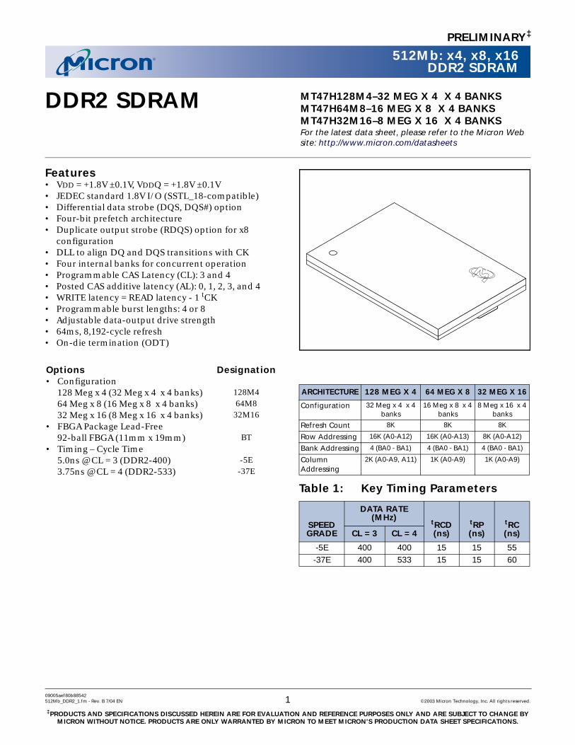
MT47H128M4–32 MEG X 4 X 4 BANKSMT47H64M8–16 MEG X 8 X 4 BANKSMT47H32M16–8 MEG X 16 X 4 BANKSFor the latest data sheet, please refer to the Micron Web site: http://www.micron.com/datasheets
Features• VDD = +1.8V ±0.1V, VDDQ = +1.8V ±0.1V• JEDEC standard 1.8V I/O (SSTL_18-compatible)• Differential data strobe (DQS, DQS#) option• Four-bit prefetch architecture• Duplicate output strobe (RDQS) option for x8
configuration• DLL to align DQ and DQS transitions with CK• Four internal banks for concurrent operation• Programmable CAS Latency (CL): 3 and 4• Posted CAS additive latency (AL): 0, 1, 2, 3, and 4• WRITE latency = READ latency - 1 tCK• Programmable burst lengths: 4 or 8• Adjustable data-output drive strength• 64ms, 8,192-cycle refresh• On-die termination (ODT)
Options Designation
• Configuration128 Meg x 4 (32 Meg x 4 x 4 banks) 128M464 Meg x 8 (16 Meg x 8 x 4 banks) 64M832 Meg x 16 (8 Meg x 16 x 4 banks) 32M16
• FBGA Package Lead-Free92-ball FBGA (11mm x 19mm) BT
• Timing – Cycle Time 5.0ns @ CL = 3 (DDR2-400) -5E3.75ns @ CL = 4 (DDR2-533) -37E
ARCHITECTURE 128 MEG X 4 64 MEG X 8 32 MEG X 16
Configuration 32 Meg x 4 x 4 banks
16 Meg x 8 x 4 banks
8 Meg x 16 x 4 banks
Refresh Count 8K 8K 8K
Row Addressing 16K (A0-A12) 16K (A0-A13) 8K (A0-A12)
Bank Addressing 4 (BA0 - BA1) 4 (BA0 - BA1) 4 (BA0 - BA1)
Column Addressing
2K (A0-A9, A11) 1K (A0-A9) 1K (A0-A9)
Table 1: Key Timing Parameters
SPEED GRADE
DATA RATE (MHz)
tRCD(ns)
tRP(ns)
tRC(ns)CL = 3 CL = 4
-5E 400 400 15 15 55-37E 400 533 15 15 60
N AND REFERENCE PURPOSES ONLY AND ARE SUBJECT TO CHANGE BY ON TO MEET MICRON’S PRODUCTION DATA SHEET SPECIFICATIONS.
©2003 Micron Technology, Inc. All rights reserved.

512Mb: x4, x8, x16DDR2 SDRAM
PRELIMINARY
Table of ContentsFeatures . . . . . . . . . . . . . . . . . . . . . . . . . . . . . . . . . . . . . . . . . . . . . . . . . . . . . . . . . . . . . . . . . . . . . . . . . . . . . . . . . . . . . . . . . . . . . .1
Options . . . . . . . . . . . . . . . . . . . . . . . . . . . . . . . . . . . . . . . . . . . . . . . . . . . . . . . . . . . . . . . . . . . . . . . . . . . . . . . . . . . . . . . . .1Part Numbers . . . . . . . . . . . . . . . . . . . . . . . . . . . . . . . . . . . . . . . . . . . . . . . . . . . . . . . . . . . . . . . . . . . . . . . . . . . . . . . . . . . . . . . . .7FBGA Part Marking Decoder. . . . . . . . . . . . . . . . . . . . . . . . . . . . . . . . . . . . . . . . . . . . . . . . . . . . . . . . . . . . . . . . . . . . . . . . . . . .7General Description . . . . . . . . . . . . . . . . . . . . . . . . . . . . . . . . . . . . . . . . . . . . . . . . . . . . . . . . . . . . . . . . . . . . . . . . . . . . . . . . . . .7Functional Description . . . . . . . . . . . . . . . . . . . . . . . . . . . . . . . . . . . . . . . . . . . . . . . . . . . . . . . . . . . . . . . . . . . . . . . . . . . . . . .13Initialization . . . . . . . . . . . . . . . . . . . . . . . . . . . . . . . . . . . . . . . . . . . . . . . . . . . . . . . . . . . . . . . . . . . . . . . . . . . . . . . . . . . . . . . . .15Mode Register (MR) . . . . . . . . . . . . . . . . . . . . . . . . . . . . . . . . . . . . . . . . . . . . . . . . . . . . . . . . . . . . . . . . . . . . . . . . . . . . . . . . . .17
Burst Length . . . . . . . . . . . . . . . . . . . . . . . . . . . . . . . . . . . . . . . . . . . . . . . . . . . . . . . . . . . . . . . . . . . . . . . . . . . . . . . . . . . . . .17Burst Type . . . . . . . . . . . . . . . . . . . . . . . . . . . . . . . . . . . . . . . . . . . . . . . . . . . . . . . . . . . . . . . . . . . . . . . . . . . . . . . . . . . . . . . .17Operating Mode . . . . . . . . . . . . . . . . . . . . . . . . . . . . . . . . . . . . . . . . . . . . . . . . . . . . . . . . . . . . . . . . . . . . . . . . . . . . . . . . . . .18DLL Reset . . . . . . . . . . . . . . . . . . . . . . . . . . . . . . . . . . . . . . . . . . . . . . . . . . . . . . . . . . . . . . . . . . . . . . . . . . . . . . . . . . . . . . . . .18Write Recovery . . . . . . . . . . . . . . . . . . . . . . . . . . . . . . . . . . . . . . . . . . . . . . . . . . . . . . . . . . . . . . . . . . . . . . . . . . . . . . . . . . . .18Power-Down Mode . . . . . . . . . . . . . . . . . . . . . . . . . . . . . . . . . . . . . . . . . . . . . . . . . . . . . . . . . . . . . . . . . . . . . . . . . . . . . . . .18CAS Latency (CL) . . . . . . . . . . . . . . . . . . . . . . . . . . . . . . . . . . . . . . . . . . . . . . . . . . . . . . . . . . . . . . . . . . . . . . . . . . . . . . . . . .18
Extended Mode Register (EMR) . . . . . . . . . . . . . . . . . . . . . . . . . . . . . . . . . . . . . . . . . . . . . . . . . . . . . . . . . . . . . . . . . . . . . . . .20DLL Enable/Disable . . . . . . . . . . . . . . . . . . . . . . . . . . . . . . . . . . . . . . . . . . . . . . . . . . . . . . . . . . . . . . . . . . . . . . . . . . . . . . . . . .20Output Drive Strength . . . . . . . . . . . . . . . . . . . . . . . . . . . . . . . . . . . . . . . . . . . . . . . . . . . . . . . . . . . . . . . . . . . . . . . . . . . . . . . .20DQS# Enable/Disable. . . . . . . . . . . . . . . . . . . . . . . . . . . . . . . . . . . . . . . . . . . . . . . . . . . . . . . . . . . . . . . . . . . . . . . . . . . . . . . . .20RDQS Enable/Disable . . . . . . . . . . . . . . . . . . . . . . . . . . . . . . . . . . . . . . . . . . . . . . . . . . . . . . . . . . . . . . . . . . . . . . . . . . . . . . . .20Output Enable/Disable . . . . . . . . . . . . . . . . . . . . . . . . . . . . . . . . . . . . . . . . . . . . . . . . . . . . . . . . . . . . . . . . . . . . . . . . . . . . . . .21On Die Termination (ODT) . . . . . . . . . . . . . . . . . . . . . . . . . . . . . . . . . . . . . . . . . . . . . . . . . . . . . . . . . . . . . . . . . . . . . . . . . . . .21Off-Chip Driver (OCD) Impedance Calibration . . . . . . . . . . . . . . . . . . . . . . . . . . . . . . . . . . . . . . . . . . . . . . . . . . . . . . . . . .22Posted CAS Additive Latency (AL) . . . . . . . . . . . . . . . . . . . . . . . . . . . . . . . . . . . . . . . . . . . . . . . . . . . . . . . . . . . . . . . . . . . . . .22Extended Mode Register 2 (EMR2) . . . . . . . . . . . . . . . . . . . . . . . . . . . . . . . . . . . . . . . . . . . . . . . . . . . . . . . . . . . . . . . . . . . . .23Extended Mode Register 3 (EMR3) . . . . . . . . . . . . . . . . . . . . . . . . . . . . . . . . . . . . . . . . . . . . . . . . . . . . . . . . . . . . . . . . . . . . .23Command Truth Tables. . . . . . . . . . . . . . . . . . . . . . . . . . . . . . . . . . . . . . . . . . . . . . . . . . . . . . . . . . . . . . . . . . . . . . . . . . . . . . .24DESELECT, NOP, and LOAD MODE Commands . . . . . . . . . . . . . . . . . . . . . . . . . . . . . . . . . . . . . . . . . . . . . . . . . . . . . . . .28
DESELECT . . . . . . . . . . . . . . . . . . . . . . . . . . . . . . . . . . . . . . . . . . . . . . . . . . . . . . . . . . . . . . . . . . . . . . . . . . . . . . . . . . . . . . . .28NO OPERATION (NOP). . . . . . . . . . . . . . . . . . . . . . . . . . . . . . . . . . . . . . . . . . . . . . . . . . . . . . . . . . . . . . . . . . . . . . . . . . . . .28LOAD MODE (LM) . . . . . . . . . . . . . . . . . . . . . . . . . . . . . . . . . . . . . . . . . . . . . . . . . . . . . . . . . . . . . . . . . . . . . . . . . . . . . . . . .28
Bank/Row Activation . . . . . . . . . . . . . . . . . . . . . . . . . . . . . . . . . . . . . . . . . . . . . . . . . . . . . . . . . . . . . . . . . . . . . . . . . . . . . . . . .29ACTIVE Command. . . . . . . . . . . . . . . . . . . . . . . . . . . . . . . . . . . . . . . . . . . . . . . . . . . . . . . . . . . . . . . . . . . . . . . . . . . . . . . . .29ACTIVE Operation . . . . . . . . . . . . . . . . . . . . . . . . . . . . . . . . . . . . . . . . . . . . . . . . . . . . . . . . . . . . . . . . . . . . . . . . . . . . . . . . .29
READs . . . . . . . . . . . . . . . . . . . . . . . . . . . . . . . . . . . . . . . . . . . . . . . . . . . . . . . . . . . . . . . . . . . . . . . . . . . . . . . . . . . . . . . . . . . . . .30READ Command . . . . . . . . . . . . . . . . . . . . . . . . . . . . . . . . . . . . . . . . . . . . . . . . . . . . . . . . . . . . . . . . . . . . . . . . . . . . . . . . . .30READ Operation . . . . . . . . . . . . . . . . . . . . . . . . . . . . . . . . . . . . . . . . . . . . . . . . . . . . . . . . . . . . . . . . . . . . . . . . . . . . . . . . . . .30
WRITEs . . . . . . . . . . . . . . . . . . . . . . . . . . . . . . . . . . . . . . . . . . . . . . . . . . . . . . . . . . . . . . . . . . . . . . . . . . . . . . . . . . . . . . . . . . . . .42WRITE Command . . . . . . . . . . . . . . . . . . . . . . . . . . . . . . . . . . . . . . . . . . . . . . . . . . . . . . . . . . . . . . . . . . . . . . . . . . . . . . . . .42WRITE Operation . . . . . . . . . . . . . . . . . . . . . . . . . . . . . . . . . . . . . . . . . . . . . . . . . . . . . . . . . . . . . . . . . . . . . . . . . . . . . . . . . .42
Precharge . . . . . . . . . . . . . . . . . . . . . . . . . . . . . . . . . . . . . . . . . . . . . . . . . . . . . . . . . . . . . . . . . . . . . . . . . . . . . . . . . . . . . . . . . . .53PRECHARGE Command . . . . . . . . . . . . . . . . . . . . . . . . . . . . . . . . . . . . . . . . . . . . . . . . . . . . . . . . . . . . . . . . . . . . . . . . . . . .53PRECHARGE Operation . . . . . . . . . . . . . . . . . . . . . . . . . . . . . . . . . . . . . . . . . . . . . . . . . . . . . . . . . . . . . . . . . . . . . . . . . . . .53
Self Refresh . . . . . . . . . . . . . . . . . . . . . . . . . . . . . . . . . . . . . . . . . . . . . . . . . . . . . . . . . . . . . . . . . . . . . . . . . . . . . . . . . . . . . . . . . .54SELF REFRESH Command . . . . . . . . . . . . . . . . . . . . . . . . . . . . . . . . . . . . . . . . . . . . . . . . . . . . . . . . . . . . . . . . . . . . . . . . . .54
REFRESH. . . . . . . . . . . . . . . . . . . . . . . . . . . . . . . . . . . . . . . . . . . . . . . . . . . . . . . . . . . . . . . . . . . . . . . . . . . . . . . . . . . . . . . . . . . .56REFRESH Command . . . . . . . . . . . . . . . . . . . . . . . . . . . . . . . . . . . . . . . . . . . . . . . . . . . . . . . . . . . . . . . . . . . . . . . . . . . . . . .56
Power-Down Mode. . . . . . . . . . . . . . . . . . . . . . . . . . . . . . . . . . . . . . . . . . . . . . . . . . . . . . . . . . . . . . . . . . . . . . . . . . . . . . . . . . .57Precharge Power-Down Clock Frequency Change . . . . . . . . . . . . . . . . . . . . . . . . . . . . . . . . . . . . . . . . . . . . . . . . . . . . . . .64RESET Function (CKE LOW Anytime) . . . . . . . . . . . . . . . . . . . . . . . . . . . . . . . . . . . . . . . . . . . . . . . . . . . . . . . . . . . . . . . . . .65ODT Timing . . . . . . . . . . . . . . . . . . . . . . . . . . . . . . . . . . . . . . . . . . . . . . . . . . . . . . . . . . . . . . . . . . . . . . . . . . . . . . . . . . . . . . . . .66
09005aef80b88542 Micron Technology, Inc., reserves the right to change products or specifications without notice.512Mb_DDR2TOC.fm - Rev. B 7/04 EN 2 ©2003 Micron Technology, Inc. All rights reserved.

512Mb: x4, x8, x16DDR2 SDRAM
PRELIMINARY
Absolute Maximum Ratings . . . . . . . . . . . . . . . . . . . . . . . . . . . . . . . . . . . . . . . . . . . . . . . . . . . . . . . . . . . . . . . . . . . . . . . . . . .73AC and DC Operating Conditions . . . . . . . . . . . . . . . . . . . . . . . . . . . . . . . . . . . . . . . . . . . . . . . . . . . . . . . . . . . . . . . . . . . . . .74Input Electrical Characteristics and Operating Conditions. . . . . . . . . . . . . . . . . . . . . . . . . . . . . . . . . . . . . . . . . . . . . . . .75Input Slew Rate Derating. . . . . . . . . . . . . . . . . . . . . . . . . . . . . . . . . . . . . . . . . . . . . . . . . . . . . . . . . . . . . . . . . . . . . . . . . . . . . .78Data Slew Rating . . . . . . . . . . . . . . . . . . . . . . . . . . . . . . . . . . . . . . . . . . . . . . . . . . . . . . . . . . . . . . . . . . . . . . . . . . . . . . . . . . . . .81Power and Ground Clamp Characteristics . . . . . . . . . . . . . . . . . . . . . . . . . . . . . . . . . . . . . . . . . . . . . . . . . . . . . . . . . . . . . .86AC Overshoot/Undershoot Specification . . . . . . . . . . . . . . . . . . . . . . . . . . . . . . . . . . . . . . . . . . . . . . . . . . . . . . . . . . . . . . .87Output Electrical Characteristics and Operating Conditions . . . . . . . . . . . . . . . . . . . . . . . . . . . . . . . . . . . . . . . . . . . . . .88Full Strength Pull-Down Driver Characteristics . . . . . . . . . . . . . . . . . . . . . . . . . . . . . . . . . . . . . . . . . . . . . . . . . . . . . . . . . .90Full Strength Pull-Up Driver Characteristics . . . . . . . . . . . . . . . . . . . . . . . . . . . . . . . . . . . . . . . . . . . . . . . . . . . . . . . . . . . .91FBGA Package Capacitance . . . . . . . . . . . . . . . . . . . . . . . . . . . . . . . . . . . . . . . . . . . . . . . . . . . . . . . . . . . . . . . . . . . . . . . . . . .92IDD Specifications and Conditions . . . . . . . . . . . . . . . . . . . . . . . . . . . . . . . . . . . . . . . . . . . . . . . . . . . . . . . . . . . . . . . . . . . . .93
IDD7 Conditions . . . . . . . . . . . . . . . . . . . . . . . . . . . . . . . . . . . . . . . . . . . . . . . . . . . . . . . . . . . . . . . . . . . . . . . . . . . . . . . . . . .95Notes . . . . . . . . . . . . . . . . . . . . . . . . . . . . . . . . . . . . . . . . . . . . . . . . . . . . . . . . . . . . . . . . . . . . . . . . . . . . . . . . . . . . . . . . . . . . . 100Data Sheet Designation . . . . . . . . . . . . . . . . . . . . . . . . . . . . . . . . . . . . . . . . . . . . . . . . . . . . . . . . . . . . . . . . . . . . . . . . . . . . . 102
09005aef80b88542 Micron Technology, Inc., reserves the right to change products or specifications without notice.512Mb_DDR2TOC.fm - Rev. B 7/04 EN 3 ©2003 Micron Technology, Inc. All rights reserved.

512Mb: x4, x8, x16DDR2 SDRAM
PRELIMINARY
List of FiguresFigure 1: 512Mb DDR2 Part Numbers . . . . . . . . . . . . . . . . . . . . . . . . . . . . . . . . . . . . . . . . . . . . . . . . . . . . . . . . . . . . . . .7Figure 2: 92-ball FBGA Ball Assignment (x16), 11mm x 19mm (Top View) . . . . . . . . . . . . . . . . . . . . . . . . . . . . . . .9Figure 3: 92-Ball FBGA Ball Assignment (x 4, x 8), 11mm x 19mm (Top View) . . . . . . . . . . . . . . . . . . . . . . . . . . . .9Figure 4: Functional Block Diagram (32 Meg x 16) . . . . . . . . . . . . . . . . . . . . . . . . . . . . . . . . . . . . . . . . . . . . . . . . . . .13Figure 5: Functional Block Diagram (64 Meg x 8) . . . . . . . . . . . . . . . . . . . . . . . . . . . . . . . . . . . . . . . . . . . . . . . . . . . .14Figure 6: Functional Block Diagram (128 Meg x 4) . . . . . . . . . . . . . . . . . . . . . . . . . . . . . . . . . . . . . . . . . . . . . . . . . . .14Figure 7: DDR2 Power-Up and Initialization. . . . . . . . . . . . . . . . . . . . . . . . . . . . . . . . . . . . . . . . . . . . . . . . . . . . . . . . .16Figure 8: Mode Register (MR) Definition . . . . . . . . . . . . . . . . . . . . . . . . . . . . . . . . . . . . . . . . . . . . . . . . . . . . . . . . . . . .17Figure 9: CAS Latency (CL) . . . . . . . . . . . . . . . . . . . . . . . . . . . . . . . . . . . . . . . . . . . . . . . . . . . . . . . . . . . . . . . . . . . . . . . .19Figure 10: Extended Mode Register Definition . . . . . . . . . . . . . . . . . . . . . . . . . . . . . . . . . . . . . . . . . . . . . . . . . . . . . . . .20Figure 11: READ Latency . . . . . . . . . . . . . . . . . . . . . . . . . . . . . . . . . . . . . . . . . . . . . . . . . . . . . . . . . . . . . . . . . . . . . . . . . . .22Figure 12: Write Latency. . . . . . . . . . . . . . . . . . . . . . . . . . . . . . . . . . . . . . . . . . . . . . . . . . . . . . . . . . . . . . . . . . . . . . . . . . . .22Figure 13: Extended Mode Register 2 (EMR2) Definition . . . . . . . . . . . . . . . . . . . . . . . . . . . . . . . . . . . . . . . . . . . . . . .23Figure 14: Extended Mode Register 3 (EMR3) Definition . . . . . . . . . . . . . . . . . . . . . . . . . . . . . . . . . . . . . . . . . . . . . . .23Figure 15: ACTIVE Command . . . . . . . . . . . . . . . . . . . . . . . . . . . . . . . . . . . . . . . . . . . . . . . . . . . . . . . . . . . . . . . . . . . . . .29Figure 16: READ Command . . . . . . . . . . . . . . . . . . . . . . . . . . . . . . . . . . . . . . . . . . . . . . . . . . . . . . . . . . . . . . . . . . . . . . . .30Figure 17: Example: Meeting tRRD (MIN) and tRCD (MIN) . . . . . . . . . . . . . . . . . . . . . . . . . . . . . . . . . . . . . . . . . . . . .30Figure 18: READ Latency . . . . . . . . . . . . . . . . . . . . . . . . . . . . . . . . . . . . . . . . . . . . . . . . . . . . . . . . . . . . . . . . . . . . . . . . . . .31Figure 19: Consecutive READ Bursts . . . . . . . . . . . . . . . . . . . . . . . . . . . . . . . . . . . . . . . . . . . . . . . . . . . . . . . . . . . . . . . . .32Figure 20: Nonconsecutive READ Bursts . . . . . . . . . . . . . . . . . . . . . . . . . . . . . . . . . . . . . . . . . . . . . . . . . . . . . . . . . . . . .33Figure 21: READ Interrupted by READ . . . . . . . . . . . . . . . . . . . . . . . . . . . . . . . . . . . . . . . . . . . . . . . . . . . . . . . . . . . . . . .34Figure 22: READ to PRECHARGE BL = 4 . . . . . . . . . . . . . . . . . . . . . . . . . . . . . . . . . . . . . . . . . . . . . . . . . . . . . . . . . . . . . .35Figure 23: READ to PRECHARGE BL = 8 . . . . . . . . . . . . . . . . . . . . . . . . . . . . . . . . . . . . . . . . . . . . . . . . . . . . . . . . . . . . . .36Figure 24: READ to WRITE . . . . . . . . . . . . . . . . . . . . . . . . . . . . . . . . . . . . . . . . . . . . . . . . . . . . . . . . . . . . . . . . . . . . . . . . . .36Figure 25: Bank Read – Without Auto Precharge . . . . . . . . . . . . . . . . . . . . . . . . . . . . . . . . . . . . . . . . . . . . . . . . . . . . . .37Figure 26: Bank Read – With Auto Precharge. . . . . . . . . . . . . . . . . . . . . . . . . . . . . . . . . . . . . . . . . . . . . . . . . . . . . . . . . .38Figure 27: x4, x8 Data Output Timing – tDQSQ, tQH, and Data Valid Window . . . . . . . . . . . . . . . . . . . . . . . . . . . .39Figure 28: x16 Data Output Timing – tDQSQ, tQH, and Data Valid Window . . . . . . . . . . . . . . . . . . . . . . . . . . . . . .40Figure 29: Data Output Timing – tAC and tDQSCK. . . . . . . . . . . . . . . . . . . . . . . . . . . . . . . . . . . . . . . . . . . . . . . . . . . . .41Figure 30: WRITE Command . . . . . . . . . . . . . . . . . . . . . . . . . . . . . . . . . . . . . . . . . . . . . . . . . . . . . . . . . . . . . . . . . . . . . . .42Figure 31: WRITE Burst. . . . . . . . . . . . . . . . . . . . . . . . . . . . . . . . . . . . . . . . . . . . . . . . . . . . . . . . . . . . . . . . . . . . . . . . . . . . .44Figure 32: Consecutive WRITE to WRITE . . . . . . . . . . . . . . . . . . . . . . . . . . . . . . . . . . . . . . . . . . . . . . . . . . . . . . . . . . . . .45Figure 33: Nonconsecutive WRITE to WRITE . . . . . . . . . . . . . . . . . . . . . . . . . . . . . . . . . . . . . . . . . . . . . . . . . . . . . . . . .45Figure 34: Random WRITE Cycles . . . . . . . . . . . . . . . . . . . . . . . . . . . . . . . . . . . . . . . . . . . . . . . . . . . . . . . . . . . . . . . . . . .46Figure 35: WRITE Interrupted by WRITE . . . . . . . . . . . . . . . . . . . . . . . . . . . . . . . . . . . . . . . . . . . . . . . . . . . . . . . . . . . . .46Figure 36: WRITE to READ . . . . . . . . . . . . . . . . . . . . . . . . . . . . . . . . . . . . . . . . . . . . . . . . . . . . . . . . . . . . . . . . . . . . . . . . . .47Figure 37: WRITE to PRECHARGE . . . . . . . . . . . . . . . . . . . . . . . . . . . . . . . . . . . . . . . . . . . . . . . . . . . . . . . . . . . . . . . . . . .48Figure 38: Bank Write–Without Auto Precharge . . . . . . . . . . . . . . . . . . . . . . . . . . . . . . . . . . . . . . . . . . . . . . . . . . . . . . .49Figure 39: Bank Write–with Auto Precharge . . . . . . . . . . . . . . . . . . . . . . . . . . . . . . . . . . . . . . . . . . . . . . . . . . . . . . . . . .50Figure 40: WRITE–DM Operation. . . . . . . . . . . . . . . . . . . . . . . . . . . . . . . . . . . . . . . . . . . . . . . . . . . . . . . . . . . . . . . . . . . .51Figure 41: Data Input Timing . . . . . . . . . . . . . . . . . . . . . . . . . . . . . . . . . . . . . . . . . . . . . . . . . . . . . . . . . . . . . . . . . . . . . . .52Figure 42: PRECHARGE Command . . . . . . . . . . . . . . . . . . . . . . . . . . . . . . . . . . . . . . . . . . . . . . . . . . . . . . . . . . . . . . . . .53Figure 43: Self Refresh. . . . . . . . . . . . . . . . . . . . . . . . . . . . . . . . . . . . . . . . . . . . . . . . . . . . . . . . . . . . . . . . . . . . . . . . . . . . . .55Figure 44: Refresh Mode. . . . . . . . . . . . . . . . . . . . . . . . . . . . . . . . . . . . . . . . . . . . . . . . . . . . . . . . . . . . . . . . . . . . . . . . . . . .56Figure 45: Power-Down . . . . . . . . . . . . . . . . . . . . . . . . . . . . . . . . . . . . . . . . . . . . . . . . . . . . . . . . . . . . . . . . . . . . . . . . . . . .58Figure 46: READ to Power-Down Entry. . . . . . . . . . . . . . . . . . . . . . . . . . . . . . . . . . . . . . . . . . . . . . . . . . . . . . . . . . . . . . .60Figure 47: READ with Auto Precharge to Power-Down Entry . . . . . . . . . . . . . . . . . . . . . . . . . . . . . . . . . . . . . . . . . . .60Figure 48: WRITE to Power-Down Entry. . . . . . . . . . . . . . . . . . . . . . . . . . . . . . . . . . . . . . . . . . . . . . . . . . . . . . . . . . . . . .61Figure 49: WRITE with Auto Precharge to Power-Down Entry . . . . . . . . . . . . . . . . . . . . . . . . . . . . . . . . . . . . . . . . . .61Figure 50: REFRESH command to Power-Down Entry . . . . . . . . . . . . . . . . . . . . . . . . . . . . . . . . . . . . . . . . . . . . . . . . .61Figure 51: ACTIVE Command to Power-Down Entry . . . . . . . . . . . . . . . . . . . . . . . . . . . . . . . . . . . . . . . . . . . . . . . . . .62Figure 52: PRECHARGE Command to Power-Down Entry . . . . . . . . . . . . . . . . . . . . . . . . . . . . . . . . . . . . . . . . . . . . .62Figure 53: LOAD MODE Command to Power-Down Entry . . . . . . . . . . . . . . . . . . . . . . . . . . . . . . . . . . . . . . . . . . . . .63Figure 54: Input Clock Frequency Change During PRECHARGE Power Down Mode . . . . . . . . . . . . . . . . . . . . . .64Figure 55: RESET Condition . . . . . . . . . . . . . . . . . . . . . . . . . . . . . . . . . . . . . . . . . . . . . . . . . . . . . . . . . . . . . . . . . . . . . . . .65Figure 56: ODT Timing for Active or “Fast-Exit” Power-Down Mode . . . . . . . . . . . . . . . . . . . . . . . . . . . . . . . . . . . .67
09005aef80b88542 Micron Technology, Inc., reserves the right to change products or specifications without notice.512Mb_DDR2LOF.fm - Rev. B 7/04 EN 4 ©2003 Micron Technology, Inc. All rights reserved.

512Mb: x4, x8, x16DDR2 SDRAM
PRELIMINARY
Figure 57: ODT timing for “Slow-Exit” or Precharge Power-Down Modes . . . . . . . . . . . . . . . . . . . . . . . . . . . . . . . .68Figure 58: ODT “Turn Off” Timings when Entering Power-Down Mode . . . . . . . . . . . . . . . . . . . . . . . . . . . . . . . . .69Figure 59: ODT “Turn-On” Timing when Entering Power-Down Mode . . . . . . . . . . . . . . . . . . . . . . . . . . . . . . . . .70Figure 60: ODT “Turn-Off” Timing when Exiting Power-Down Mode . . . . . . . . . . . . . . . . . . . . . . . . . . . . . . . . . . .71Figure 61: ODT “Turn On” Timing when Exiting Power-Down Mode . . . . . . . . . . . . . . . . . . . . . . . . . . . . . . . . . . .72Figure 62: Example Temperature Test Point Location . . . . . . . . . . . . . . . . . . . . . . . . . . . . . . . . . . . . . . . . . . . . . . . . .73Figure 63: Single-Ended Input Signal Levels . . . . . . . . . . . . . . . . . . . . . . . . . . . . . . . . . . . . . . . . . . . . . . . . . . . . . . . . . .75Figure 64: Differential Input Signal Levels . . . . . . . . . . . . . . . . . . . . . . . . . . . . . . . . . . . . . . . . . . . . . . . . . . . . . . . . . . . .76Figure 65: Nominal Slew Rate for tIS . . . . . . . . . . . . . . . . . . . . . . . . . . . . . . . . . . . . . . . . . . . . . . . . . . . . . . . . . . . . . . . . .79Figure 66: Tangent Line for tIS . . . . . . . . . . . . . . . . . . . . . . . . . . . . . . . . . . . . . . . . . . . . . . . . . . . . . . . . . . . . . . . . . . . . . .79Figure 67: Nominal Slew Rate for tIH. . . . . . . . . . . . . . . . . . . . . . . . . . . . . . . . . . . . . . . . . . . . . . . . . . . . . . . . . . . . . . . . .80Figure 68: Tangent Line for tIH . . . . . . . . . . . . . . . . . . . . . . . . . . . . . . . . . . . . . . . . . . . . . . . . . . . . . . . . . . . . . . . . . . . . . .80Figure 69: Nominal Slew Rate for tDS . . . . . . . . . . . . . . . . . . . . . . . . . . . . . . . . . . . . . . . . . . . . . . . . . . . . . . . . . . . . . . . .82Figure 70: Tangent Line for tDS . . . . . . . . . . . . . . . . . . . . . . . . . . . . . . . . . . . . . . . . . . . . . . . . . . . . . . . . . . . . . . . . . . . . .82Figure 71: Nominal Slew Rate for tDH. . . . . . . . . . . . . . . . . . . . . . . . . . . . . . . . . . . . . . . . . . . . . . . . . . . . . . . . . . . . . . . .83Figure 72: Tangent Line for tDH . . . . . . . . . . . . . . . . . . . . . . . . . . . . . . . . . . . . . . . . . . . . . . . . . . . . . . . . . . . . . . . . . . . . .83Figure 73: AC Input Test Signal Waveform Command/Address pins. . . . . . . . . . . . . . . . . . . . . . . . . . . . . . . . . . . . .84Figure 74: AC Input Test Signal Waveform for Data with DQS,DQS# (differential) . . . . . . . . . . . . . . . . . . . . . . . .84Figure 75: AC Input Test Signal Waveform for Data with DQS (single-ended) . . . . . . . . . . . . . . . . . . . . . . . . . . . .85Figure 76: AC Input Test Signal Waveform (differential). . . . . . . . . . . . . . . . . . . . . . . . . . . . . . . . . . . . . . . . . . . . . . . .85Figure 77: Input Clamp Characteristics . . . . . . . . . . . . . . . . . . . . . . . . . . . . . . . . . . . . . . . . . . . . . . . . . . . . . . . . . . . . . .86Figure 78: Overshoot . . . . . . . . . . . . . . . . . . . . . . . . . . . . . . . . . . . . . . . . . . . . . . . . . . . . . . . . . . . . . . . . . . . . . . . . . . . . . . .87Figure 79: Undershoot . . . . . . . . . . . . . . . . . . . . . . . . . . . . . . . . . . . . . . . . . . . . . . . . . . . . . . . . . . . . . . . . . . . . . . . . . . . . .87Figure 80: Differential Output Signal Levels . . . . . . . . . . . . . . . . . . . . . . . . . . . . . . . . . . . . . . . . . . . . . . . . . . . . . . . . . .88Figure 81: Output Slew Rate Load . . . . . . . . . . . . . . . . . . . . . . . . . . . . . . . . . . . . . . . . . . . . . . . . . . . . . . . . . . . . . . . . . . .89Figure 82: Full Strength Pull-Down Characteristics . . . . . . . . . . . . . . . . . . . . . . . . . . . . . . . . . . . . . . . . . . . . . . . . . . . .90Figure 83: Full Strength Pull-up Characteristics . . . . . . . . . . . . . . . . . . . . . . . . . . . . . . . . . . . . . . . . . . . . . . . . . . . . . . .91Figure 84: Package Drawing (x4,x8,x16 Configurations) 11mm x 19mm FBGA . . . . . . . . . . . . . . . . . . . . . . . . . . 102
09005aef80b88542 Micron Technology, Inc., reserves the right to change products or specifications without notice.512Mb_DDR2LOF.fm - Rev. B 7/04 EN 5 ©2003 Micron Technology, Inc. All rights reserved.

512Mb: x4, x8, x16DDR2 SDRAM
PRELIMINARY
09005aef80b88542 Micron Technology, Inc., reserves the right to change products or specifications without notice.512Mb_DDR2LOT.fm - Rev. B 7/04 EN 6 ©2003 Micron Technology, Inc. All rights reserved.
List of TablesTable 1: Key Timing Parameters . . . . . . . . . . . . . . . . . . . . . . . . . . . . . . . . . . . . . . . . . . . . . . . . . . . . . . . . . . . . . . . . . . . .1Table 2: FBGA Ball Descriptions 128 Meg x 4, 64 Meg x 8, 32 Meg x 16 . . . . . . . . . . . . . . . . . . . . . . . . . . . . . . . . .10Table 3: Burst Definition. . . . . . . . . . . . . . . . . . . . . . . . . . . . . . . . . . . . . . . . . . . . . . . . . . . . . . . . . . . . . . . . . . . . . . . . . .18Table 4: Truth Table – DDR2 Commands . . . . . . . . . . . . . . . . . . . . . . . . . . . . . . . . . . . . . . . . . . . . . . . . . . . . . . . . . . .24Table 5: Truth Table – Current State Bank n - Command to Bank n. . . . . . . . . . . . . . . . . . . . . . . . . . . . . . . . . . . .25Table 6: Truth Table – Current State Bank n - Command to Bank m . . . . . . . . . . . . . . . . . . . . . . . . . . . . . . . . . . .27Table 7: READ Using Concurrent Auto Precharge . . . . . . . . . . . . . . . . . . . . . . . . . . . . . . . . . . . . . . . . . . . . . . . . . . .35Table 8: WRITE Using Concurrent Auto Precharge . . . . . . . . . . . . . . . . . . . . . . . . . . . . . . . . . . . . . . . . . . . . . . . . . .43Table 9: CKE Truth Table . . . . . . . . . . . . . . . . . . . . . . . . . . . . . . . . . . . . . . . . . . . . . . . . . . . . . . . . . . . . . . . . . . . . . . . . .59Table 10: ODT Timing for Active and “Fast-Exit” Power-Down Modes . . . . . . . . . . . . . . . . . . . . . . . . . . . . . . . . . .67Table 11: ODT timing for “Slow-Exit” and Precharge Power-Down Modes . . . . . . . . . . . . . . . . . . . . . . . . . . . . . .68Table 12: ODT “Turn Off” Timings when Entering Power-Down Mode . . . . . . . . . . . . . . . . . . . . . . . . . . . . . . . . .69Table 13: ODT “Turn-On” Timing when Entering Power-Down Mode . . . . . . . . . . . . . . . . . . . . . . . . . . . . . . . . . .70Table 14: ODT “Turn-Of” Timing when Exiting Power-Down Mode . . . . . . . . . . . . . . . . . . . . . . . . . . . . . . . . . . . .71Table 15: ODT “Turn On” Timing when Exiting Power-Down Mode . . . . . . . . . . . . . . . . . . . . . . . . . . . . . . . . . . . .72Table 16: Absolute Maximum DC Ratings . . . . . . . . . . . . . . . . . . . . . . . . . . . . . . . . . . . . . . . . . . . . . . . . . . . . . . . . . . .73Table 17: Recommended DC Operating Conditions (SSTL_18). . . . . . . . . . . . . . . . . . . . . . . . . . . . . . . . . . . . . . . . .74Table 18: ODT DC Electrical Characteristics . . . . . . . . . . . . . . . . . . . . . . . . . . . . . . . . . . . . . . . . . . . . . . . . . . . . . . . . .74Table 19: Input DC Logic Levels . . . . . . . . . . . . . . . . . . . . . . . . . . . . . . . . . . . . . . . . . . . . . . . . . . . . . . . . . . . . . . . . . . . .75Table 20: Input AC Logic Levels . . . . . . . . . . . . . . . . . . . . . . . . . . . . . . . . . . . . . . . . . . . . . . . . . . . . . . . . . . . . . . . . . . . .75Table 21: Differential Input Logic Levels. . . . . . . . . . . . . . . . . . . . . . . . . . . . . . . . . . . . . . . . . . . . . . . . . . . . . . . . . . . . .76Table 22: AC Input Test Conditions . . . . . . . . . . . . . . . . . . . . . . . . . . . . . . . . . . . . . . . . . . . . . . . . . . . . . . . . . . . . . . . . .77Table 23: Setup and Hold Time Derating Values. . . . . . . . . . . . . . . . . . . . . . . . . . . . . . . . . . . . . . . . . . . . . . . . . . . . . .78Table 24: tDS, tDH Derating Values . . . . . . . . . . . . . . . . . . . . . . . . . . . . . . . . . . . . . . . . . . . . . . . . . . . . . . . . . . . . . . . . .81Table 25: Input Clamp Characteristics . . . . . . . . . . . . . . . . . . . . . . . . . . . . . . . . . . . . . . . . . . . . . . . . . . . . . . . . . . . . . .86Table 26: Address and Control Pins . . . . . . . . . . . . . . . . . . . . . . . . . . . . . . . . . . . . . . . . . . . . . . . . . . . . . . . . . . . . . . . . .87Table 27: Clock, Data, Strobe, and Mask Pins . . . . . . . . . . . . . . . . . . . . . . . . . . . . . . . . . . . . . . . . . . . . . . . . . . . . . . . .87Table 28: Differential AC Output Parameters. . . . . . . . . . . . . . . . . . . . . . . . . . . . . . . . . . . . . . . . . . . . . . . . . . . . . . . . .88Table 29: Output DC Current Drive . . . . . . . . . . . . . . . . . . . . . . . . . . . . . . . . . . . . . . . . . . . . . . . . . . . . . . . . . . . . . . . . .89Table 30: Output Characteristics. . . . . . . . . . . . . . . . . . . . . . . . . . . . . . . . . . . . . . . . . . . . . . . . . . . . . . . . . . . . . . . . . . . .89Table 31: Pulldown Current (mA) . . . . . . . . . . . . . . . . . . . . . . . . . . . . . . . . . . . . . . . . . . . . . . . . . . . . . . . . . . . . . . . . . . .90Table 32: Pull-Up Current (mA) . . . . . . . . . . . . . . . . . . . . . . . . . . . . . . . . . . . . . . . . . . . . . . . . . . . . . . . . . . . . . . . . . . . .91Table 33: Input Capacitance . . . . . . . . . . . . . . . . . . . . . . . . . . . . . . . . . . . . . . . . . . . . . . . . . . . . . . . . . . . . . . . . . . . . . . .92Table 34: DDR2 IDD Specifications and Conditions . . . . . . . . . . . . . . . . . . . . . . . . . . . . . . . . . . . . . . . . . . . . . . . . . . .93Table 35: General IDD Parameters . . . . . . . . . . . . . . . . . . . . . . . . . . . . . . . . . . . . . . . . . . . . . . . . . . . . . . . . . . . . . . . . . .94Table 36: IDD7 Timing Patterns . . . . . . . . . . . . . . . . . . . . . . . . . . . . . . . . . . . . . . . . . . . . . . . . . . . . . . . . . . . . . . . . . . . . .95Table 37: AC Operating Conditions . . . . . . . . . . . . . . . . . . . . . . . . . . . . . . . . . . . . . . . . . . . . . . . . . . . . . . . . . . . . . . . . .96

512Mb: x4, x8, x16DDR2 SDRAM
PRELIMINARY
Part NumbersFigure 1: 512Mb DDR2 Part Numbers
NOTE: Not all speeds and configurations are avail-able.
FBGA Part Marking DecoderDue to space limitations, FBGA-packaged compo-
nents have an abbreviated part marking that is differ-ent from the part number. Micron's new FBGA PartMarking Decoder makes it easier to understand thatpart marking. Visit the web site at www.micron.com/decoder.
General DescriptionThe 512Mb DDR2 SDRAM is a high-speed, CMOS
dynamic random-access memory containing5,368,709 bits. It is internally configured as a quad-bank DRAM. The functional block diagrams of the 32Meg x 16, 64 Meg x 8, and 128 Meg x 4 devices, respec-tively are shown in the Functional Description section.Ball assignments for the 128 Meg x 4 are shown inFigure 2 and signal descriptions are shown in Table 1.Ball assignments for the 64 Meg x 8 and 128 Meg x 4 areshown in Figure 2 and signal descriptions are shown inTable 2.
The 512Mb DDR2 SDRAM uses a double data ratearchitecture to achieve high-speed operation. Thedouble data rate architecture is essentially a 4n-prefetch architecture with an interface designed totransfer two data words per clock cycle at the I/O pins.A single read or write access for the 512Mb DDR2SDRAM effectively consists of a single 4n-bit-wide,one-clock-cycle data transfer at the internal DRAMcore and four corresponding n-bit-wide, one-half-clock-cycle data transfers at the I/O pins.
A bidirectional data strobe (DQS, DQS#) is transmit-ted externally, along with data, for use in data captureat the receiver. DQS is a strobe transmitted by theDDR2 SDRAM during READs and by the memory con-troller during WRITEs. DQS is edge-aligned with datafor READs and center-aligned with data for WRITEs.The x16 offering has two data strobes, one for the lowerbyte (LDQS, LDQS#) and one for the upper byte(UDQS, UDQS#).
The 512Mb DDR2 SDRAM operates from a differen-tial clock (CK and CK#); the crossing of CK going HIGHand CK# going LOW will be referred to as the positiveedge of CK. Commands (address and control signals)are registered at every positive edge of CK. Input datais registered on both edges of DQS, and output data isreferenced to both edges of DQS, as well as to bothedges of CK.
Read and write accesses to the DDR2 SDRAM areburst-oriented; accesses start at a selected locationand continue for a programmed number of locationsin a programmed sequence. Accesses begin with theregistration of an ACTIVE command, which is then fol-lowed by a READ or WRITE command. The addressbits registered coincident with the ACTIVE commandare used to select the bank and row to be accessed.The address bits registered coincident with the READor WRITE command are used to select the bank andthe starting column location for the burst access.
The DDR2 SDRAM provides for programmable reador write burst lengths of four or eight locations. DDR2SDRAM supports interrupting a burst read of eightwith another read, or a burst write of eight withanother write. An auto precharge function may beenabled to provide a self-timed row precharge that isinitiated at the end of the burst access.
As with standard DDR SDRAMs, the pipelined,multibank architecture of DDR2 SDRAMs allows forconcurrent operation, thereby providing high, effec-tive bandwidth by hiding row precharge and activationtime.
A self refresh mode is provided, along with a power-saving power-down mode.
All inputs are compatible with the JEDEC standardfor SSTL_18. All full drive-strength outputs areSSTL_18-compatible.
NOTE: 1. The functionality and the timing specifica-tions discussed in this data sheet are for theDLL-enabled mode of operation.
2. Throughout the data sheet, the various fig-ures and text refer to DQs as “DQ.” The DQterm is to be interpreted as any and all DQ
- ConfigurationMT47H Package Speed
Configuration
128 Meg x 4
64 Meg x 8
32 Meg x 16
128M4
64M8
32M16
Package
92-Ball 11 x 19 FBGA
BT
Example Part Number: MT47H64M8FT-37E
Speed Grade
tCK = 5ns, CL = 3
tCK = 3.75ns, CL = 4
-5E
-37E
09005aef80b88542 Micron Technology, Inc., reserves the right to change products or specifications without notice.512Mb_DDR2_2.fm - Rev. B 7/04 EN 7 ©2003 Micron Technology, Inc. All rights reserved.
512Mb: x4, x8, x16DDR2 SDRAM
PRELIMINARY
collectively, unless specifically stated other-wise. Additionally, the x16 is divided intotwo bytes, the lower byte and upper byte.For the lower byte (DQ0 through DQ7) DMrefers to LDM and DQS refers to LDQS. Forthe upper byte (DQ8 through DQ15) DMrefers to UDM and DQS refers to UDQS.
3. Complete functionality is describedthroughout the document and any page ordiagram may have been simplified to con-vey a topic and may not be inclusive of allrequirements.
4. Any specific requirement takes precedenceover a general statement.
09005aef80b88542 Micron Technology, Inc., reserves the right to change products or specifications without notice.512Mb_DDR2_2.fm - Rev. B 7/04 EN 8 ©2003 Micron Technology, Inc. All rights reserved.

512Mb: x4, x8, x16DDR2 SDRAM
PRELIMINARY
Figure 2: 92-ball FBGA Ball Assignment (x16), 11mm x 19mm (Top View)
Figure 3: 92-Ball FBGA Ball Assignment (x 4, x 8), 11mm x 19mm (Top View)
1 2 3 4 6 7 8 95
A
B
C
D
E
F
G
H
J
K
L
M
N
P
R
T
U
V
W
Y
AA
NC
VDD
DQ14
VDDQ
DQ12
VDD
DQ6
VDDQ
DQ4
VDDL
BA2
VSS
VDD
NC
NC
NC
VSSQ
DQ9
VSSQ
NC
VSSQ
DQ1
VSSQ
VREF
CKE
BA0
A10
A3
A7
A12
NC
VSS
UDM
VDDQ
DQ11
VSS
LDM
VDDQ
DQ3
VSS
WE#
BA1
A1
A5
A9
RFU
VSSQ
UDQS
VDDQ
DQ10
VSSQ
LDQS
VDDQ
DQ2
VSSDL
RAS#
CAS#
A2
A6
A11
RFU
NC
VDDQ
DQ15
VDDQ
DQ13
VDDQ
DQ7
VDDQ
DQ5
VDD
ODT
VDD
VSS
NC
NC
UDQS#/NU
VSSQ
DQ8
VSSQ
LDQS#/NU
VSSQ
DQ0
VSSQ
CK
CK#
CS#
A0
A4
A8
NC
NC
1 2 3 4 6 7 8 95
VDD
NC
NC
NC
VDD
NF,DQ6
VDDQ
NF,DQ4
VDDL
BA2
VSS
VDD
NC
NC
NC
NC
NC
NC
NF, RDQS#/NU
VSSQ
DQ1
VSSQ
VREF
CKE
BA0
A10
A3
A7
A12
NC
VSS
NC
NC
NC
VSS
DM,DM/RDQS
VDDQ
DQ3
VSS
WE#
BA1
A1
A5
A9
RFU
VSSQ
NC
NC
NC
VSSQ
DQS
VDDQ
DQ2
VSSDL
RAS#
CAS#
A2
A6
A11
RFU
NC
VDDQ
NC
NC
NC
VDDQ
NF,DQ7
VDDQ
NF,DQ5
VDD
ODT
VDD
VSS
NC
NC
NC
NC
NC
NC
DQS#/NU
VSSQ
DQ0
VSSQ
CK
CK#
CS#
A0
A4
A8
A13
NC
A
B
C
D
E
F
G
H
J
K
L
M
N
P
R
T
U
V
W
Y
AA
NC
09005aef80b88542 Micron Technology, Inc., reserves the right to change products or specifications without notice.512Mb_DDR2_2.fm - Rev. B 7/04 EN 9 ©2003 Micron Technology, Inc. All rights reserved.

512Mb: x4, x8, x16DDR2 SDRAM
PRELIMINARY
Table 2: FBGA Ball Descriptions 128 Meg x 4, 64 Meg x 8, 32 Meg x 16
x16 FBGA BALL
ASSIGNMENT
x4, x8 FBGA BALL
ASSIGNMENT SYMBOL TYPE DESCRIPTION
N9 N9 ODT Input On-Die Termination: ODT (registered HIGH) enables termination resistance internal to the DDR2 SDRAM. When enabled, ODT is only applied to each of the following pins: DQ0–DQ15, LDM, UDM, LDQS, LDQS#, UDQS, and UDQS# for the x16; DQ0-DQ7, DQS, DQS#, RDQS, RDQS#, and DM for the x8; DQ0-DQ3, DQS, DQS#, and DM for the x4. The ODT input will be ignored if disabled via the LOAD MODE command.
M8, N8 M8, N8 CK, CK# Input Clock: CK and CK# are differential clock inputs. All address and control input signals are sampled on the crossing of the positive edge of CK and negative edge of CK#. Output data (DQs and DQS/DQS#) is referenced to the crossings of CK and CK#.
N2 N2 CKE Input Clock Enable: CKE (registered HIGH) activates and CKE (registered LOW) deactivates clocking circuitry on the DDR2 SDRAM. The specific circuitry that is enabled/disabled is dependent on the DDR2 SDRAM configuration and operating mode. CKE LOW provides PRECHARGE POWER-DOWN and SELF REFRESH operations (all banks idle), or ACTIVE POWER-DOWN (row ACTIVE in any bank). CKE is synchronous for POWER-DOWN entry, POWER-DOWN exit, output disable, and for SELF REFRESH entry. CKE is asynchronous for SELF REFRESH exit. Input buffers (excluding CK, CK#, CKE, and ODT) are disabled during POWER-DOWN. Input buffers (excluding CKE) are disabled during SELF REFRESH. CKE is an SSTL_18 input but will detect a LVCMOS LOW level once VDD is applied during first power-up. After Vref has become stable during the power on and initialization sequence, it must be maintained for proper operation of the CKE receiver. For proper self-refresh operation VREF must be maintained.
P8 P8 CS# Input Chip Select: CS# enables (registered LOW) and disables (registered HIGH) the command decoder. All commands are masked when CS# is registered HIGH. CS# provides for external bank selection on systems with multiple ranks. CS# is considered part of the command code.
N7, P7, N3 N7, P7, N3 RAS#, CAS#, WE#
Input Command Inputs: RAS#, CAS#, and WE# (along with CS#) define the command being entered.
J3, E3 J3 LDM, UDM Input Input Data Mask: DM is an input mask signal for write data. Input data is masked when DM is sampled HIGH along with that input data during a WRITE access. DM is sampled on both edges of DQS. Although DM pins are input-only, the DM loading is designed to match that of DQ and DQS pins. LDM is DM for lower byte DQ0–DQ7 and UDM is DM for upper byte DQ8–DQ15.
P2, P3 P2, P3 BA0-BA1 Input Bank Address Inputs: BA0-BA2 define to which bank an ACTIVE, READ, WRITE, or PRECHARGE command is being applied. BA0-BA2 define which mode register including MR, EMR, EMR(2), and EMR(3) is loaded during the LOAD MODE command.
09005aef80b88542 Micron Technology, Inc., reserves the right to change products or specifications without notice.512Mb_DDR2_2.fm - Rev. B 7/04 EN 10 ©2003 Micron Technology, Inc. All rights reserved.

512Mb: x4, x8, x16DDR2 SDRAM
PRELIMINARY
R8,R3,R7,T2,T8,T3,T7,U2,U8,U3,R2,U7,
V2
– A0–A3A4–A7A8–A11
A12
Input Address Inputs: Provide the row address for ACTIVE commands, and the column address and auto precharge bit (A10) for Read/Write commands, to select one location out of the memory array in the respective bank. A10 sampled during a PRECHARGE command determines whether the PRECHARGE applies to one bank (A10 LOW, bank selected by BA1-BA0) or all banks (A10 HIGH). The address inputs also provide the op-code during a LOAD MODE command.
– R8,R3,R7,T2,T8,T3,T7,U2,U8,U3,R2,U7,
V2,V8
A0–A3A4–A7A8–A11A12-A13
Input Address Inputs: Provide the row address for ACTIVE commands, and the column address and auto precharge bit (A10) for Read/Write commands, to select one location out of the memory array in the respective bank. A10 sampled during a PRECHARGE command determines whether the PRECHARGE applies to one bank (A10 LOW, bank selected by BA1-BA0) or all banks (A10 HIGH). The address inputs also provide the op-code during a LOAD MODE command.
K8,K2,L7,L3,L1,L9,J1,J9,
F8,F2,G7,G3,G1,G9,E1,E9
– DQ0–DQ3DQ4–DQ7
DQ8–DQ11DQ12–DQ15
I/O Data Input/Output: Bidirectional data bus for 32 Meg x 16.
– K8,K2,L7,L3,L1,L9,J1,J9
DQ0–DQ3DQ4–DQ7
I/O Data Input/Output: Bidirectional data bus for 64 Meg x 8.
– K8,K2,L7,L3 DQ0–DQ3 I/O Data Input/Output: Bidirectional data bus for 128 Meg x 4.E7,D8 – UDQS,
UDQS#I/O Data Strobe for Upper Byte: Output with read data, input with
write data for source synchronous operation. Edge-aligned with read data, center-aligned with write data. UDQS# is only used when differential data strobe mode is enabled via the LOAD MODE command.
J7,H8 – LDQS, LDQS#
I/O Data Strobe for Lower Byte: Output with read data, input with write data for source synchronous operation. Edge-aligned with read data, center-aligned with write data. LDQS# is only used when differential data strobe mode is enabled via the LOAD MODE command.
– J7,H8 DQS, DQS# I/O Data Strobe: Output with read data, input with write data for source synchronous operation. Edge-aligned with read data, center aligned with write data. DQS# is only used when differential data strobe mode is enabled via the LOAD MODE command.
– J3,H2 RDQS, RDQS#
Output Redundant Data Strobe for 64 Meg x 8 only. RDQS is enabled/disabled via the LOAD MODE command to the Extended Mode Register (EMR). When RDQS is enabled, RDQS is output with read data only and is ignored during write data. When RDQS is disabled, pin J3 becomes Data Mask (see DM pin). RDQS# is only used when RDQS is enabled AND differential data strobe mode is enabled.
D1,H1,M9,R9,V1
D1,H1,M9,R9,V1
VDD Supply Power Supply: 1.8V ±0.1V.
M1 M1 VDDL Supply DLL Power Supply: 1.8V ±0.1V.
Table 2: FBGA Ball Descriptions 128 Meg x 4, 64 Meg x 8, 32 Meg x 16
x16 FBGA BALL
ASSIGNMENT
x4, x8 FBGA BALL
ASSIGNMENT SYMBOL TYPE DESCRIPTION
09005aef80b88542 Micron Technology, Inc., reserves the right to change products or specifications without notice.512Mb_DDR2_2.fm - Rev. B 7/04 EN 11 ©2003 Micron Technology, Inc. All rights reserved.

512Mb: x4, x8, x16DDR2 SDRAM
PRELIMINARY
D9,F1,F3,F7,F9,H9,K1,K3,
K7,K9
D9,H9,K1,K3,K7,K9
VDDQ Supply DQ Power Supply: 1.8V ±0.1V. Isolated on the device for improved noise immunity.
M2 M2 VREF Supply SSTL_18 reference voltage.D3,H3,M3,T1,
U9D3,H3,M3,T1,
U9VSS Supply Ground.
M7 M7 VSSDL Supply DLL Ground. Isolated on the device from VSS and VSSQ.D7,E2,E8,G2,G8,H7, J2,J8,
L2,L8
D7,H7,J2,J8,L2,L8
VSSQ Supply DQ Ground. Isolated on the device for improved noise immunity.
A1,A2,A8,A9D2,H2,V8,
AA1,AA2,AA8,AA9
A1,A2,A8,A9,D2,D8,E1-E3,E7-E9,F1-F3,
F7-F9, G1-G3,G7-G9,
AA1,AA2,AA8,AA9
NC – No Connect: These pins should be left unconnected.
– J1, J9, L1, L9, H2,
NF – No Function: These pins are used as DQ4-DQ7 on the 64 Meg x 8, but are NF (No Function) on the 128 Meg x 4 configuration.
D8, H8 - NU – x16 only Not Used: If EMR[E10] = 0, D8 and H8 are UDQS# and LDQS#. If EMR[E10] = 1, then D8 and H8 are Not Used.
- H2, H8 NU – X8 only Not Used: If EMR[E10] = 0, H2 and H8 are RDQS# and DQS#. If EMR[E10] = 1, then H2 and H8 are Not Used.
V3, V7 V3, V7 RFU – Reserved for Future Use; Row address bits A14(V3) and A15(V7) are reserved for 2Gb and 4Gb densities.
Table 2: FBGA Ball Descriptions 128 Meg x 4, 64 Meg x 8, 32 Meg x 16
x16 FBGA BALL
ASSIGNMENT
x4, x8 FBGA BALL
ASSIGNMENT SYMBOL TYPE DESCRIPTION
09005aef80b88542 Micron Technology, Inc., reserves the right to change products or specifications without notice.512Mb_DDR2_2.fm - Rev. B 7/04 EN 12 ©2003 Micron Technology, Inc. All rights reserved.

512Mb: x4, x8, x16DDR2 SDRAM
PRELIMINARY
Figure 4: Functional DescriptionThe 512Mb DDR2 SDRAM is a high-speed, CMOS
dynamic random-access memory containing1,073,741,824 bits. The 512Mb DDR2 SDRAM is inter-nally configured as a four-bank DRAM.
The 512Mb DDR2 SDRAM uses a double data ratearchitecture to achieve high-speed operation. TheDDR2 architecture is essentially a 4n-prefetch archi-tecture, with an interface designed to transfer two datawords per clock cycle at the I/O pins. A single read or
write access for the 512Mb DDR2 SDRAM consists of asingle 4n-bit-wide, one-clock-cycle data transfer at theinternal DRAM core and four corresponding n-bit-wide, one-half-clock-cycle data transfers at the I/Opins.
Prior to normal operation, the DDR2 SDRAM mustbe initialized. The following sections provide detailedinformation covering device initialization, register def-inition, command descriptions, and device operation.
Figure 5: Functional Block Diagram (32 Meg x 16)
13
ROW-ADDRESS
MUX
CONTROLLOGIC
COLUMN-ADDRESSCOUNTER/
LATCH
MODE REGISTERS
10
A0-A12,BA0, BA1
13
ADDRESSREGISTER
15
256(x64)
16,384
I/O GATINGDM MASK LOGIC
COLUMNDECODER
BANK0MEMORY
ARRAY(8,192 x 256 x 64)
BANK0ROW-
ADDRESSLATCH
&DECODER
8,192
SENSE AMPLIFIERS
BANKCONTROL
LOGIC
15
BANK1BANK2
BANK3
13
8
2
2
REFRESHCOUNTER
16
16
16
4
RCVRS
64
64
64
CK OUT
DATA
UDQS, UDQS#LDQS, LDQS#
CK,CK#
CK,CK#
COL0,COL1
COL0,COL1
CK IN
DRVRS
DLL
MUX
DQSGENERATOR
16
16
16
16
16
UDQS, UDQS#LDQS, LDQS#
4
READLATCH
WRITEFIFO
&DRIVERS
DATA
16
16
16
1664
2
2
2
2
MASK
2
2
2
228
16
16
2
BANK1BANK2
BANK3
INPUTREGISTERS
UDM, LDM
DQ0 - DQ15
VDDQ
R1
R1
R2
R2
sw1 sw2
VssQ
R1
R1
R2
R2
sw1 sw2
R1
R1
R2
R2
sw1 sw2
sw1 sw2
ODT CONTROL
RAS#
CAS#
CK
CS#
WE#
CK#
CO
MM
AN
D
DEC
OD
E
CKE
ODT
09005aef80b88542 Micron Technology, Inc., reserves the right to change products or specifications without notice.512Mb_DDR2_2.fm - Rev. B 7/04 EN 13 ©2003 Micron Technology, Inc. All rights reserved.

512Mb: x4, x8, x16DDR2 SDRAM
PRELIMINARY
Figure 6: Functional Block Diagram (64 Meg x 8)
Figure 7: Functional Block Diagram (128 Meg x 4)
14
ROW-ADDRESS
MUX
CONTROLLOGIC
COLUMN-ADDRESSCOUNTER/
LATCH
MODE REGISTERS
10
CO
MM
AN
D
DEC
OD
E
A0-A13,BA0, BA1
14
ADDRESSREGISTER
16
256(x32)
8,192
I/O GATINGDM MASK LOGIC
COLUMNDECODER
BANK0MEMORY
ARRAY(16,384 x 256 x 32)
BANK0ROW-
ADDRESSLATCH
&DECODER
16,384
SENSE AMPLIFIERS
BANKCONTROL
LOGIC
16
BANK1BANK2
BANK3
14
8
2
2
REFRESHCOUNTER
8
8
8
2
RCVRS
32
32
32
CK OUT
DATA
DQS, DQS#
InternalCK,CK#
CK,CK#
COL0,COL1
COL0,COL1
CK IN
DRVRS
DLL
MUX
DQSGENERATOR
8
8
8
8
8
DQ0 - DQ7
DQS, DQS#
2
READLATCH
WRITEFIFO
&DRIVERS
DATA
8
8
8
832
1
1
1
1
MASK
1
1
1
114
8
8
2
BANK1BANK2
BANK3
INPUTREGISTERS
DM
RDQS#
VDDQ
R1
R1
R2
R2
sw1 sw2
VssQ
R1
R1
R2
R2
sw1 sw2
R1
R1
R2
R2
sw1 sw2
sw1 sw2
ODT CONTROLRAS#
CAS#
CK
CS#
WE#
CK#
CKE
RDQS
ODT
14
RAS#
CAS#
ROW-ADDRESS
MUX
CK
CS#
WE#
CK#
CONTROLLOGIC
COLUMN-ADDRESSCOUNTER/
LATCH
MODE REGISTERS
11
CO
MM
AN
D
DEC
OD
E
A0-A13,BA0, BA1
CKE
14
ADDRESSREGISTER
16
512(x16)
8,192
I/O GATINGDM MASK LOGIC
COLUMNDECODER
BANK0MEMORY
ARRAY(16,384 x 512 x 16)
BANK0ROW-
ADDRESSLATCH
&DECODER
16,384
SENSE AMPLIFIERS
BANKCONTROL
LOGIC
16
BANK1BANK2
BANK3
14
9
2
2
REFRESHCOUNTER
4
4
4
2
RCVRS
16
16
16
CK OUT
DATA
DQS, DQS#
InternalCK, CK#
CK, CK#
COL0,COL1
COL0,COL1
CK IN
DRVRS
DLL
MUX
DQSGENERATOR
4
4
4
4
4
DQ0 - DQ3
DQS, DQS#
2
READLATCH
WRITEFIFO
&DRIVERS
DATA
4
4
4
416
1
1
1
1
MASK
1
1
1
114
4
4
2
BANK1BANK2
BANK3
INPUTREGISTERS
DM
VDDQ
R1
R1
R2
R2
sw1 sw2
VssQ
R1
R1
R2
R2
sw1 sw2
R1
R1
R2
R2
sw1 sw2
ODT
sw1 sw2
ODT CONTROL
09005aef80b88542 Micron Technology, Inc., reserves the right to change products or specifications without notice.512Mb_DDR2_2.fm - Rev. B 7/04 EN 14 ©2003 Micron Technology, Inc. All rights reserved.

512Mb: x4, x8, x16DDR2 SDRAM
PRELIMINARY
InitializationThe following sequence is required for power-up
and initialization and is shown in Figure 8.1. Apply power; if CKE is maintained below 0.2*
VDDQ, outputs remain disabled. To guarantee RTT
(ODT Resistance) is off, VREF must be valid and alow level must be applied to the ODT pin (all otherinputs may be undefined). The time from whenVDD first starts to power-up to the completion ofVDDQ must be equal to or less than 10ms. At leastone of the following two sets of conditions (A or B)must be met:A. CONDITION SET A
• VDD, VDDL and VDDQ are driven from a single power converter output
• VTT is limited to 0.95V MAX• VREF tracks VDDQ/2.
B. CONDITION SET B• Apply VDD before or at the same time as VDDL.• Apply VDDL before or at the same time as VDDQ.• Apply VDDQ before or at the same time as VTT
and VREF. • The voltage difference between any VDD supply
can not exceed 0.5V. For a minimum of 200µs after stable power and clock (CK, CK#), apply NOP or DESELECT commands and take CKE HIGH.
2. Wait a minimum of 400ns, then issue a PRE-CHARGE ALL command.
3. Issue an LOAD MODE command to the EMR(2)register. (To issue an EMR(2) command, provideLOW to BA0, provide HIGH to BA1.)
4. Issue a LOAD MODE command to the EMR(3)register. (To issue an EMR(3) command, provideHIGH to BA0 and BA1.)
5. Issue an LOAD MODE command to the EMR reg-ister to enable DLL. To issue a DLL ENABLE com-mand, provide LOW to BA1 and A0, provide HIGHto BA0. Bits E7, E8, and E9 must all be set to 0.
6. Issue a LOAD MODE command for DLL Reset.200 cycles of clock input is required to lock theDLL. (To issue a DLL Reset, provide HIGH to A8and provide LOW to BA1 and BA0.) CKE must beHIGH the entire time.
7. Issue PRECHARGE ALL command.8. Issue two or more REFRESH commands.9. Issue a LOAD MODE command with LOW to A8 to
initialize device operation (i.e., to program oper-ating parameters without resetting the DLL).
10. Issue a LOAD MODE command to the EMR toenable OCD default by setting Bits E7, E8, and E9to 1 and set all other desired parameters.
11. Issue a LOAD MODE command to the EMR toenable OCD exit by setting Bits E7, E8, and E9 to 0and set all other desired parameters.
12. The DDR2 SDRAM is now intialized and ready fornormal operation 200 clocks after DLL Reset instep 6.
09005aef80b88542 Micron Technology, Inc., reserves the right to change products or specifications without notice.512Mb_DDR2_2.fm - Rev. B 7/04 EN 15 ©2003 Micron Technology, Inc. All rights reserved.

512Mb: x4, x8, x16DDR2 SDRAM
PRELIMINARY
Figure 8: DDR2 Power-Up and Initialization
NOTE:
1. VTT is not applied directly to the device; however, tVTD should be greater than or equal to zero to avoid device latch-up.The time from when VDD first starts to power-up to the completion of VDDQ must be equal to or less than 10ms. One of the following two conditions (a or b) MUST be met:
a) VDD, VDDL, and VDDQ are driven from a single power converter output.VTT may be 0.95V maximum during power up.VREF tracks VDDQ/2.b) Apply VDD before or at the same time as VDDL.Apply VDDL before or at the same time as VDDQ.Apply VDDQ before or at the same time as VTT and VREF. The voltage difference between any VDD supply can not exceed 0.5V.
2. Either a NOP or DESELECT command may be applied.3. 200 cycles of clock (CK, CK#) are required before a READ command can be issued. CKE must be HIGH the entire time.4. Two or more REFRESH commands are required.5. Bits E7, E8, and E9 must all be set to 0 with all other operating parameters of EMRS set as required.6. PRE = PRECHARGE command, LM = LOAD MODE command, REF = REFRESH command, ACT = ACTIVE command, RA =
Row Address, BA = Bank Address.7. DM represents DM for x4, x8 configuration and UDM, LDM for x16 configuration. DQS represents DQS, DQS#, UDQS,
UDQS#, LDQS, LDQS#, RDQS, RDQS# for the appropriate configuration (x4, x8, x16). DQ represents DQ0–DQ3 for x4, DQ0–DQ7 for x8, and DQ0–DQ15 for x16.
8. CKE pin uses LVCMOS input levels prior to state T0. After state T0, CKE pin uses SSTL_18 input levels. 9. ADDRESS represents A12-A0 for x4, x8, and A12-A0 for x16, BA0-BA1. A10 should be HIGH at states Tb0 and Tg0 to
ensure a PRECHARGE (all banks) command is issued.10. Bits E7, E8, and E9 must be set to 1 to set OCD default.11. Bits E7, E8, and E9 must be set to 0 to set OCD exit and all other operating parameters of EMRS set as required.
tVTD1
CKE
Rtt
Power-up:VDD and stableclock (CK, CK#)
T = 200µs (min)
High-Z
DM7
DQS7High-Z
ADDRESS10
CK
CK#
tCL
VTT1
VREF
VDDL
VDDQ
COMMAND6 NOP2 PRE
T0 Ta0
DON’T CARE
tCL
tCK
VDD
ODT
DQ7 High-Z
T = 400ns (min)
Tb0
200 cycles of CK3
EMR withDLL Enable5
MR withDLL Reset
tMRD tMRD t tRFC tRFC
CODE9
LM PRELM5 REF4 REF4 LM10
CODE10 CODE10 CODE10
Tg0 Th0 Ti0 Tj0
MR w/oDLL Resett
EMR withOCD Default
tMRD tMRD tMRD
Tk0 Tl0 Tm0Te0 Tf0
EMR(2)9 EMR(3)9
tMRD tMRD
LM9LM9
CODE10CODE10 CODE10
tRPA
Tc0 Td0
LVCMOS LOW LEVEL8
SSTL_18 LOW LEVEL8
VALID3
VALID
Indicates a break in time scale
RPA
LM11
CODE9
EMR withOCD Exit
LM12
CODE9
NormalOperation
09005aef80b88542 Micron Technology, Inc., reserves the right to change products or specifications without notice.512Mb_DDR2_2.fm - Rev. B 7/04 EN 16 ©2003 Micron Technology, Inc. All rights reserved.

512Mb: x4, x8, x16DDR2 SDRAM
PRELIMINARY
Mode Register (MR)The mode register is used to define the specific
mode of operation of the DDR2 SDRAM. This defini-tion includes the selection of a burst length, burst type,CAS latency, operating mode, DLL reset, write recov-ery, and power-down mode as shown in Figure 9. Con-tents of the mode register can be altered by re-executing the LOAD MODE (LM) command. If theuser chooses to modify only a subset of the MR vari-ables, all variables (M0–M14) must be programmedwhen the LOAD MODE command is issued.
The mode register is programmed via the LM com-mand (bits BA1-BA0 = 0, 0) and other bits (M13 - M0for x4 and x8, M12 - M0 for x16) will retain the storedinformation until it is programmed again or the deviceloses power (except for bit M8, which is self-clearing).Reprogramming the mode register will not alter thecontents of the memory array, provided it is performedcorrectly.
The LOAD MODE command can only be issued (orreissued) when all banks are in the precharged state.The controller must wait the specified time tMRDbefore initiating any subsequent operations such as anACTIVE command. Violating either of these require-ments will result in unspecified operation.
Burst LengthBurst length is defined by bits M0–M3 as shown in
Figure 9. Read and write accesses to the DDR2 SDRAMare burst-oriented, with the burst length being pro-grammable to either four or eight. The burst lengthdetermines the maximum number of column loca-tions that can be accessed for a given READ or WRITEcommand.
When a READ or WRITE command is issued, a blockof columns equal to the burst length is effectivelyselected. All accesses for that burst take place withinthis block, meaning that the burst will wrap within theblock if a boundary is reached. The block is uniquelyselected by A2–Ai when the burst length is set to fourand by A3–Ai when the burst length is set to eight(where Ai is the most significant column address bit fora given configuration). The remaining (least signifi-
cant) address bit(s) is (are) used to select the startinglocation within the block. The programmed burstlength applies to both READ and WRITE bursts.
Figure 9: Mode Register (MR) Definition
Burst TypeAccesses within a given burst may be programmed
to be either sequential or interleaved. The burst type isselected via bit M3 as shown in Figure 9. The orderingof accesses within a burst is determined by the burstlength, the burst type, and the starting column addressas shown in Table 3. DDR2 SDRAM supports 4-bitburst and 8-bit burst modes only. For 8-bit burst mode,full interleave address ordering is supported; however,sequential address ordering is nibble-based.
Burst LengthCAS# Latency BTPD
A9 A7 A6 A5 A4 A3A8 A2 A1 A0
Mode Register (Mx)
Address Bus
9 7 6 5 4 38 2 1 0
A10A12 A11BA0BA1
101112130*
14
*M13 (A13) is reserved for future use and must be programmed to '0.' A13 is not used in x16 configuration.
Burst Length
Reserved
Reserved
4
8
Reserved
Reserved
Reserved
Reserved
M0
0
1
0
1
0
1
0
1
M1
0
0
1
1
0
0
1
1
M2
0
0
0
0
1
1
1
1
0
1
Burst Type
Sequential
Interleaved
M3
CAS Latency
Reserved
Reserved
Reserved
3
4
Reserved
Reserved
Reserved
M4
0
1
0
1
0
1
0
1
M5
0
0
1
1
0
0
1
1
M6
0
0
0
0
1
1
1
1
0
1
Mode
Normal
Test
M7
15DLL TM
0
1
DLL Reset
No
Yes
M8
WRITE RECOVERY
Reserved
2
3
4
5
6
Reserved
Reserved
M9
0
1
0
1
0
1
0
1
M10
0
0
1
1
0
0
1
1
M11
0
0
0
0
1
1
1
1
WR
A13
MR
0
1
0
1
Mode Register Definition
Mode Register (MR)
Extended Mode Register (EMR)
Extended Mode Register (EMR2)
Extended Mode Register (EMR3)
M15
0
0
1
1
0
1
PD mode
Fast Exit
(Normal)
Slow Exit
(Low Power)
M12
M14
09005aef80b88542 Micron Technology, Inc., reserves the right to change products or specifications without notice.512Mb_DDR2_2.fm - Rev. B 7/04 EN 17 ©2003 Micron Technology, Inc. All rights reserved.

512Mb: x4, x8, x16DDR2 SDRAM
PRELIMINARY
Operating ModeThe normal operating mode is selected by issuing a
LOAD MODE command with bit M7 set to zero, and allother bits set to the desired values as shown inFigure 9. When bit M7 is ‘1,’ no other bits of the moderegister are programmed. Programming bit M7 to ‘1’places the DDR2 SDRAM into a test mode that is onlyused by the Manufacturer and should NOT be used. Nooperation or functionality is guaranteed if M7 bit is ‘1.’
DLL ResetDLL reset is defined by bit M8 as shown in Figure 9.
Programming bit M8 to ‘1’ will activate the DLL RESETfunction. Bit M8 is self-clearing, meaning it returnsback to a value of ‘0’ after the DLL RESET function hasbeen issued.
Anytime the DLL RESET function is used, 200 clockcycles must occur before a READ command can beissued to allow time for the internal clock to be syn-chronized with the external clock. Failing to wait forsynchronization to occur may result in a violation ofthe tAC or tDQSCK parameters.
Write RecoveryWrite recovery (WR) time is defined by bits M9–M11
as shown in Figure 9. The WR Register is used by theDDR2 SDRAM during WRITE with AUTO PRECHARGEoperation. During WRITE with AUTO PRECHARGEoperation, the DDR2 SDRAM delays the internal AUTOPRECHARGE operation by WR clocks (programmed in
bits M9–M11) from the last data burst. An example ofWrite with AUTO PRECHARGE is shown in Figure 26on page 30.
Write Recovery (WR) values of 2, 3, 4, 5, or 6 clocksmay be used for programming bits M9–M11. The useris required to program the value of write recovery,which is calculated by dividing tWR (in ns) by tCK (inns) and rounding up a noninteger value to the nextinteger; WR [cycles] = tWR [ns] / tCK [ns]. Reservedstates should not be used as unknown operation orincompatibility with future versions may result.
Power-Down ModeActive power-down (PD) mode is defined by bit M12
as shown in Figure 9. PD mode allows the user todetermine the active power-down mode, which deter-mines performance vs. power savings. PD mode bitM12 does not apply to precharge power-down mode.
When bit M12 = 0, standard Active Power-downmode or ‘fast-exit’ active power-down mode isenabled. The tXARD parameter is used for ‘fast-exit’active power-down exit timing. The DLL is expected tobe enabled and running during this mode.
When bit M12 = 1, a lower power active power-downmode or ‘slow-exit’ active power-down mode isenabled. The tXARDS parameter is used for ‘slow-exit’active power-down exit timing. The DLL can beenabled, but ‘frozen’ during active power-down modesince the exit-to-READ command timing is relaxed.The power difference expected between PD ‘normal’and PD ‘low-power’ mode is defined in the IDD table.
CAS Latency (CL)The CAS Latency (CL) is defined by bits M4–M6 as
shown in Figure 9. CAS Latency is the delay, in clockcycles, between the registration of a READ commandand the availability of the first bit of output data. TheCAS Latency can be set to 3 or 4 clocks. CAS Latency of2 or 5 clocks are JEDEC optional features and may beenabled in future speed grades. DDR2 SDRAM doesnot support any half clock latencies. Reserved statesshould not be used as unknown operation or incom-patibility with future versions may result.
DDR2 SDRAM also supports a feature called PostedCAS additive latency (AL). This feature allows theREAD command to be issued prior to tRCD(MIN) bydelaying the internal command to the DDR2 SDRAMby AL clocks. The AL feature is described in more detailin the Extended Mode Register (EMR) and Operationalsections.
Table 3: Burst Definition
BURST LENGTH
STARTING COLUMN ADDRESS (A2, A1,
A0)
ORDER OF ACCESSES WITHIN A BURST
BURST TYPE = SEQUENTIAL
BURST TYPE = INTERLEAVED
4 0 0 0 0,1,2,3 0,1,2,30 0 1 1,2,3,0 1,0,3,20 1 0 2,3,0,1 2,3,0,10 1 1 3,0,1,2 3,2,1,0
8 0 0 0 0,1,2,3,4,5,6,7 0,1,2,3,4,5,6,70 0 1 1,2,3,0,5,6,7,4 1,0,3,2,5,4,7,60 1 0 2,3,0,1,6,7,4,5 2,3,0,1,6,7,4,50 1 1 3,0,1,2,7,4,5,6 3,2,1,0,7,6,5,41 0 0 4,5,6,7,0,1,2,3 4,5,6,7,0,1,2,31 0 1 5,6,7,4,1,2,3,0 5,4,7,6,1,0,3,21 1 0 6,7,4,5,2,3,0,1 6,7,4,5,2,3,0,11 1 1 7,4,5,6,3,0,1,2 7,6,5,4,3,2,1,0
09005aef80b88542 Micron Technology, Inc., reserves the right to change products or specifications without notice.512Mb_DDR2_2.fm - Rev. B 7/04 EN 18 ©2003 Micron Technology, Inc. All rights reserved.

512Mb: x4, x8, x16DDR2 SDRAM
PRELIMINARY
Examples of CL = 3 and CL = 4 are shown inFigure 10; both assume AL = 0. If a READ command isregistered at clock edge n, and the CAS Latency is mclocks, the data will be available nominally coincidentwith clock edge n + m (this assumes AL = 0).
Figure 10: CAS Latency (CL)
DOUT
n + 3DOUT
n + 2DOUT
n + 1
CK
CK#
COMMAND
DQ
DQS, DQS#
CL = 3 (AL = 0)
READ
Burst length = 4Posted CAS# additive latency (AL) = 0Shown with nominal tAC, tDQSCK, and tDQSQ
T0 T1 T2
DON’T CARETRANSITIONING DATA
NOP NOP NOP
DOUT
n
T3 T4 T5
NOP NOP
T6
NOP
DOUT
n + 3DOUT
n + 2DOUT
n + 1
CK
CK#
COMMAND
DQ
DQS, DQS#
CL = 4 (AL = 0)
READ
T0 T1 T2
NOP NOP NOP
DOUT
n
T3 T4 T5
NOP NOP
T6
NOP
09005aef80b88542 Micron Technology, Inc., reserves the right to change products or specifications without notice.512Mb_DDR2_2.fm - Rev. B 7/04 EN 19 ©2003 Micron Technology, Inc. All rights reserved.

512Mb: x4, x8, x16DDR2 SDRAM
PRELIMINARY
Extended Mode Register (EMR)The extended mode register controls functions
beyond those controlled by the mode register; theseadditional functions are DLL enable/disable, outputdrive strength, ODT (RTT), Posted CAS additive latency(AL), off-chip driver impedance calibration (OCD),DQS# enable/disable, RDQS/RDQS# enable/disable,and OUTPUT disable/enable. These functions arecontrolled via the bits shown in Figure 11. Theextended mode register is programmed via the LOADMODE (LM) command and will retain the stored infor-mation until it is programmed again or the deviceloses power. Reprogramming the extended mode reg-ister will not alter the contents of the memory array,provided it is performed correctly.
The extended mode register must be loaded whenall banks are idle and no bursts are in progress, and thecontroller must wait the specified time tMRD beforeinitiating any subsequent operation. Violating either ofthese requirements could result in unspecified opera-tion.
Figure 11: Extended Mode Register Definition
DLL Enable/DisableThe DLL may be enabled or disabled by program-
ming bit E0 during the LOAD MODE command asshown in Figure 11. The DLL must be enabled for nor-mal operation. DLL enable is required during power-up initialization and upon returning to normal opera-tion after having disabled the DLL for the purpose ofdebugging or evaluation. Enabling the DLL shouldalways be followed by resetting the DLL using a LOADMODE command.
The DLL is automatically disabled when enteringself refresh operation and is automatically re-enabledand reset upon exit of self refresh operation.
Any time the DLL is enabled (and subsequentlyreset), 200 clock cycles must occur before a READcommand can be issued to allow time for the internalclock to be synchronized with the external clock. Fail-ing to wait for synchronization to occur may result in aviolation of the tAC or tDQSCK parameters.
Output Drive StrengthThe output drive strength is defined by bit E1 as
shown in Figure 11. The normal drive strength for alloutputs are specified to be SSTL_18. Programming bitE1 = 0 selects normal (100 percent) drive strength forall outputs. Selecting a reduced drive strength option(bit E1 = 1) will reduce all outputs to approximately 60percent of the SSTL_18 drive strength. This option isintended for the support of the lighter load and/orpoint-to-point environments.
DQS# Enable/DisableThe DQS# enable function is defined by bit E10.
When enabled (bit E10 = 0), DQS# is the complementof the differential data strobe pair DQS/DQS#. Whendisabled (bit E10 = 1), DQS is used in a single-endedmode and the DQS# pin is disabled. This function isalso used to enable/disable RDQS#. If RDQS is enabled(E11 = 1) and DQS# is enabled (E10 = 0), then bothDQS# and RDQS# will be enabled.
RDQS Enable/DisableThe RDQS enable function is defined by bit E11 as
shown in Figure 11. This feature is only applicable tothe x8 configuration. When enabled (E11 = 1), RDQS isidentical in function and timing to data strobe DQSduring a READ. During a WRITE operation, RDQS isignored by the DDR2 SDRAM.
DLLPosted CAS# Rttout
A9 A7 A6 A5 A4 A3A8 A2 A1 A0
Extended Mode
Register (Ex)
Address Bus
9 7 6 5 4 38 2 1 0
A10A12 A11BA0BA1
10111213
0*
14
0
1
Output Drive Strength
100%
60%
E1
Posted CAS# Additive Latency (AL)
0
1
2
3
4
Reserved
Reserved
Reserved
E3
0
1
0
1
0
1
0
1
E4
0
0
1
1
0
0
1
1
E5
0
0
0
0
1
1
1
1
0
1
DLL Enable
Enable (Normal)
Disable (Test/Debug)
E0
15
0
1
RDQS Enable
No
Yes
E11
OCD Program
A13
ODSRttDQS#
0
1
DQS# Enable
Enable
Disable
E10
RDQS
Rtt (nominal)
Rtt Disabled
75Ω
150Ω
50Ω
E2
0
1
0
1
E6
0
0
1
1
0
1
Outputs
Enabled
Disabled
E12
0
1
0
1
Mode Register Set
Mode Register Set (MRS)
Extended Mode Register (EMRS)
Extended Mode Register (EMRS2)
Extended Mode Register (EMRS3)
E15
0
0
1
1
E14
MRS
*E13 (A13) is not used on the x16 configuration.
OCD Operation
OCD Not Supported
Reserved
Reserved
Reserved
Reserved
E7
0
1
0
0
1
E8
0
0
1
0
1
E9
0
0
0
1
1
09005aef80b88542 Micron Technology, Inc., reserves the right to change products or specifications without notice.512Mb_DDR2_2.fm - Rev. B 7/04 EN 20 ©2003 Micron Technology, Inc. All rights reserved.

512Mb: x4, x8, x16DDR2 SDRAM
PRELIMINARY
Output Enable/DisableThe OUTPUT enable function is defined by bit E12
as shown in Figure 11. When enabled (E12 = 0), all out-puts (DQs, DQS, DQS#, RDQS, RDQS#) function nor-mally. When disabled (E12 = 1), all DDR2 SDRAMoutputs (DQs, DQS, DQS#, RDQS, RDQS#) are disabledremoving output buffer current. The OUTPUT disablefeature is intended to be used during IDD characteriza-tion of read current.
On Die Termination (ODT)ODT effective resistance RTT(EFF ) is defined by bits
E2 and E6 of the EMR as shown in Figure 11. The ODTfeature is designed to improve signal integrity of thememory channel by allowing the DDR2 SDRAM con-troller to independently turn on/off ODT for any or alldevices. RTT effective resistance values of 75Ω and150Ω are selectable and apply to each DQ, DQS/DQS#,RDQS/RDQS#, UDQS/UDQS#, LDQS/LDQS#, DM,and UDM/LDM signals. A functional representation ofODT is shown in block diagrams in “FunctionalDescription” on page 13. Bits (E6, E2) determine whatODT resistance is enabled by turning on/off ‘sw1’ or
‘sw2’. The ODT effective resistance value is selected byenabling switch ‘sw1,’ which enables all ‘R1’ valuesthat are 150Ω each, enabling an effective resistance of75Ω (RTT1(EFF) = ‘R1’ / 2). Similarly, if ‘sw2’ is enabled,all ‘R2’ values that are 300Ω each, enable an effectiveODT resistance of 150Ω (RTT2(EFF) = ‘R2’/2). Reservedstates should not be used, as unknown operation orincompatibility with future versions may result.
The ODT control pin is used to determine whenRTT(EFF ) is turned on and off, assuming ODT has beenenabled via bits E2 and E6 of the EMR. The ODT fea-ture and ODT input pin are only used during active,active power-down (both fast-exit and slow-exitmodes), and precharge power-down modes of opera-tion. If SELF REFRESH operation is used, RTT(EFF )should always be disabled and the ODT input pin isdisabled by the DDR2 SDRAM. During power-up andinitialization of the DDR2 SDRAM, ODT should be dis-abled until the EMR command is issued to enable theODT feature, at which point the ODT pin will deter-mine the RTT(EFF ) value. See “ODT Timing” on page 9for ODT timing diagrams.
09005aef80b88542 Micron Technology, Inc., reserves the right to change products or specifications without notice.512Mb_DDR2_2.fm - Rev. B 7/04 EN 21 ©2003 Micron Technology, Inc. All rights reserved.

512Mb: x4, x8, x16DDR2 SDRAM
PRELIMINARY
Off-Chip Driver (OCD) Impedance CalibrationThe OCD function is no longer supported and must
be set to the default state. See “Initialization” onpage 15 to propertly set OCD defaults.
Posted CAS Additive Latency (AL)Posted CAS additive latency (AL) is supported to
make the command and data bus efficient for sustain-able bandwidths in DDR2 SDRAM. Bits E3–E5 definethe value of AL as shown in Figure 11. Bits E3–E5 allowthe user to program the DDR2 SDRAM with a CAS#Additive latency of 0, 1, 2, 3, or 4 clocks. Reserved statesshould not be used as unknown operation or incom-patibility with future versions may result.
In this operation, the DDR2 SDRAM allows a READor WRITE command to be issued prior to tRCD (MIN)with the requirement that AL ≤ tRCD(MIN). A typicalapplication using this feature would set AL = tRCD(MIN) - 1 x tCK. The READ or WRITE command is heldfor the time of the additive latency (AL) before it isissued internally to the DDR2 SDRAM device. READLatency (RL) is controlled by the sum of the PostedCAS additive latency (AL) and CAS Latency (CL); RL =AL + CL. Write latency (WL) is equal to READ latencyminus one clock; WL = AL + CL - 1 x tCK. An exampleof a READ latency is shown in Figure 12. An example ofa WRITE latency is shown in Figure 13.
Figure 12: READ Latency
Figure 13: Write Latency
DOUT
n + 3DOUT
n + 2DOUT
n + 1
CK
CK#
COMMAND
DQ
DQS, DQS#
AL = 2
ACTIVE n
Burst length = 4 Shown with nominal tAC, tDQSCK, and tDQSQ
T0 T1 T2
DON’T CARETRANSITIONING DATA
READ n NOP NOP
DOUT
n
T3 T4 T5
NOP
T6
NOP
T7 T8
NOP NOP
CL = 3
RL = 5
CAS# latency (CL) = 3Additive latency (AL) = 2READ latency (RL) = AL + CL = 5
tRCD (MIN)
NOP
CK
CK#
COMMAND
DQ
DQS, DQS#
ACTIVE n
Burst length = 4
T0 T1 T2
DON’T CARETRANSITIONING DATA
NOP NOP
T3 T4 T5
NOPWRITE n
T6
NOP
Din
n + 3Din
n + 2Din
n + 1
WL = AL + CL - 1 = 4
T7
NOP
Din
n
CAS# latency (CL) = 3Additive latency (AL) = 2WRITE latency = AL + CL -1 = 4
tRCD (MIN)
NOP
AL = 2 CL - 1 = 2
09005aef80b88542 Micron Technology, Inc., reserves the right to change products or specifications without notice.512Mb_DDR2_2.fm - Rev. B 7/04 EN 22 ©2003 Micron Technology, Inc. All rights reserved.

512Mb: x4, x8, x16DDR2 SDRAM
PRELIMINARY
Extended Mode Register 2 (EMR2)The Extended Mode Register 2 (EMR2) controls
functions beyond those controlled by the mode regis-ter. Currently all bits in EMR2 are reserved as shown inFigure 14. The EMR2 is programmed via the LOADMODE command and will retain the stored informa-tion until it is programmed again or the device losespower. Reprogramming the extended mode registerwill not alter the contents of the memory array, pro-vided it is performed correctly.
The extended mode register must be loaded whenall banks are idle and no bursts are in progress, and thecontroller must wait the specified time tMRD beforeinitiating any subsequent operation. Violating eitherof these requirements could result in unspecified oper-ation.
Figure 14: Extended Mode Register 2 (EMR2) Definition
Extended Mode Register 3 (EMR3)The Extended Mode Register 3 (EMR3) controls
functions beyond those controlled by the mode regis-ter. Currently all bits in EMR3 are reserved as shown inFigure 15. The EMR3 is programmed via the LOADMODE command and will retain the stored informa-tion until it is programmed again or the device losespower. Reprogramming the extended mode registerwill not alter the contents of the memory array, pro-vided it is performed correctly.
The extended mode register must be loaded whenall banks are idle and no bursts are in progress, and thecontroller must wait the specified time tMRD beforeinitiating any subsequent operation. Violating either ofthese requirements could result in unspecified opera-tion.
Figure 15: Extended Mode Register 3 (EMR3) Definition
A9 A7 A6 A5 A4 A3A8 A2 A1 A0
Extended Mode
Register (Ex)
Address Bus
9 7 6 5 4 38 2 1 0
A10A12 A11BA0BA1
101112130*
14
* E13 (A13) - E0 (A0) are reserved for futureuse and must all be programmed to '0'.A13 is not used in x16 configuration.
15
A13
0
1
0
1
Mode Register Definition
Mode Register (MR)
Extended Mode Register (EMR)
Extended Mode Register (EMR2)
Extended Mode Register (EMR3)
M15
0
0
1
1
M14
EMR2 0* 0* 0* 0* 0* 0* 0* 0* 0* 0* 0* 0* 0*
A9 A7 A6 A5 A4 A3A8 A2 A1 A0
Extended Mode
Register (Ex)
Address Bus
9 7 6 5 4 38 2 1 0
A10A12 A11BA0BA1
101112130*
1415
A13
0
1
0
1
Mode Register Definition
Mode Register (MR)
Extended Mode Register (EMR)
Extended Mode Register (EMR2)
Extended Mode Register (EMR3)
M15
0
0
1
1
M14
EMR3 0* 0* 0* 0* 0* 0* 0* 0* 0* 0* 0* 0* 0*
* E13 (A13) - E0 (A0) are reserved for futureuse and must all be programmed to '0'.A13 is not used in x16 configuration.
09005aef80b88542 Micron Technology, Inc., reserves the right to change products or specifications without notice.512Mb_DDR2_2.fm - Rev. B 7/04 EN 23 ©2003 Micron Technology, Inc. All rights reserved.

512Mb: x4, x8, x16DDR2 SDRAM
PRELIMINARY
Command Truth TablesThe following tables provide a quick reference of
DDR2 SDRAM available commands, including CKEpower-down modes, and bank-to-bank commands.
NOTE:
1. All DDR2 SDRAM commands are defined by states of CS#, RAS#, CAS#, WE#, and CKE at the rising edge of the clock.2. Bank addresses (BA) BA1-BA0 determine which bank is to be operated upon. BA during a Load Mode command selects
which mode register is programmed.3. Burst reads or writes at BL = 4 cannot be terminated or interrupted. See sections “Read Interrupted by a Read” and
“Write Interrupted by a Write” for other restrictions and details.4. The Power Down Mode does not perform any refresh operations. The duration of power-down is therefore limited by
the refresh requirements outlined in the AC parametric section.5. The state of ODT does not affect the states described in this table. The ODT function is not available during self refresh.
See the ODT section for details.6. “X” means “H or L” (but a defined logic level).7. Self refresh exit is asynchronous.
Table 4: Truth Table – DDR2 CommandsNotes: 1, 5, and 6 apply to the entire Table.
FUNCTIONCKE
CS# RAS# CAS# WE# BA1 BA0
A12 A11 A10 A9–A0 NOTESPREVIOUS
CYCLECURRENT
CYCLE
Load Mode H H L L L L BA OP Code 2Refresh H H L L L H X X X XSelf Refresh Entry H L L L L H X X X X
Self Refresh Exit L HH X X X
X X X X 7L H H H
Single Bank Precharge
H H L L H L BA X L X 2
ALL Banks Precharge H H L L H L X X H XBank Activate H H L L H H BA Row Address
Write H H L H L L BAColumn Address
LColumn Address
2, 3
Write with Auto Precharge
H H L H L L BAColumn Address
HColumn Address
2, 3
Read H H L H L H BAColumn Address
LColumn Address
2, 3
Read with Auto Precharge
H H L H L H BAColumn Address
HColumn Address
2, 3
No Operation H X L H H H X X X XDevice Deselect H X H X X X X X X X
Power-Down Entry H LH X X X
X X X X 4L H H H
Power-Down Exit L HH X X X
X X X X 4L H H H
09005aef80b88542 Micron Technology, Inc., reserves the right to change products or specifications without notice.512Mb_DDR2_2.fm - Rev. B 7/04 EN 24 ©2003 Micron Technology, Inc. All rights reserved.

512Mb: x4, x8, x16DDR2 SDRAM
PRELIMINARY
NOTE:
1. This table applies when CKEn - 1 was HIGH and CKEn is HIGH (see Table 5) and after tXSNR has been met (if the previous state was self refresh).
2. This table is bank-specific, except where noted (i.e., the current state is for a specific bank and the commands shown are those allowed to be issued to that bank when in that state). Exceptions are covered in the notes below.
3. Current state definitions:
Idle: The bank has been precharged, and tRP has been met.
Row Active: A row in the bank has been activated, and tRCD has been met. No data bursts/accesses and no reg-ister accesses are in progress.Read: A READ burst has been initiated, with auto precharge disabled, and has not yet terminated.Write: A WRITE burst has been initiated, with auto precharge disabled, and has not yet terminated.
4. The following states must not be interrupted by a command issued to the same bank. DESELECT or NOP commands, or allowable commands to the other bank, should be issued on any clock edge occurring during these states. Allowable commands to the other bank are determined by its current state and Table 5, and according to Table 6.
Precharging: Starts with registration of a PRECHARGE command and ends when tRP is met. Once tRP is met, the bank will be in the idle state.
Row Activating: Starts with registration of an ACTIVE command and ends when tRCD is met. Once tRCD is met, the bank will be in the “row active” state.Read with Auto Precharge Enabled: Starts with registration of a READ command with auto precharge enabled
and ends when tRP has been met. Once tRP is met, the bank will be in the idle state.Write with Auto Precharge Enabled: Starts with registration of a WRITE command with auto precharge enabled
and ends when tRP has been met. Once tRP is met, the bank will be in the idle state.5. The following states must not be interrupted by any executable command; DESELECT or NOP commands must be
applied on each positive clock edge during these states.
Refreshing: Starts with registration of an REFRESH command and ends when tRFC is met. Once tRFC is met, the DDR2 SDRAM will be in the all banks idle state.
Accessing Mode Register: Starts with registration of a LOAD MODE command and ends when tMRD has been
met. Once tMRD is met, the DDR2 SDRAM will be in the all banks idle state.
Precharging All: Starts with registration of a PRECHARGE ALL command and ends when tRP is met. Once tRP is met, all banks will be in the idle state.
6. All states and sequences not shown are illegal or reserved.
Table 5: Truth Table – Current State Bank n - Command to Bank nNotes: 1–6; notes appear below and on next page.
CURRENT STATE CS# RAS# CAS# WE# COMMAND/ACTION NOTES
Any H X X X DESELECT (NOP/continue previous operation)L H H H NO OPERATION (NOP/continue previous
operation)Idle L L H H ACTIVE (select and activate row)
L L L H REFRESH 7L L L L LOAD MODE 7
Row Active L H L H READ (select column and start READ burst) 9L H L L WRITE (select column and start WRITE burst) 9L L H L PRECHARGE (deactivate row in bank or banks) 8
Read (Auto-Precharge Disabled
L H L H READ (select column and start new READ burst) 9L H L L WRITE (select column and start WRITE burst) 9, 11L L H L PRECHARGE ( start precharge) 8
Write (Auto-Precharge Disabled)
L H L H READ (select column and start READ burst) 9, 10L H L L WRITE (select column and start new WRITE burst) 9L L H L PRECHARGE (start precharge) 8, 10
09005aef80b88542 Micron Technology, Inc., reserves the right to change products or specifications without notice.512Mb_DDR2_2.fm - Rev. B 7/04 EN 25 ©2003 Micron Technology, Inc. All rights reserved.

512Mb: x4, x8, x16DDR2 SDRAM
PRELIMINARY
7. Not bank-specific; requires that all banks are idle, and bursts are not in progress.8. May or may not be bank-specific; if multiple banks are to be precharged, each must be in a valid state for precharging.9. READs or WRITEs listed in the Command/Action column include READs or WRITEs with auto precharge enabled and
READs or WRITEs with auto precharge disabled.10. Requires appropriate DM masking.11. A WRITE command may be applied after the completion of the READ burst.
09005aef80b88542 Micron Technology, Inc., reserves the right to change products or specifications without notice.512Mb_DDR2_2.fm - Rev. B 7/04 EN 26 ©2003 Micron Technology, Inc. All rights reserved.

512Mb: x4, x8, x16DDR2 SDRAM
PRELIMINARY
NOTE:
1. This table applies when CKEn - 1 was HIGH and CKEn is HIGH (see Truth Table 2) and after tXSNR has been met (if the previous state was self refresh).
2. This table describes alternate bank operation, except where noted (i.e., the current state is for bank n and the com-mands shown are those allowed to be issued to bank m, assuming that bank m is in such a state that the given com-mand is allowable). Exceptions are covered in the notes below.
3. Current state definitions:
Idle: The bank has been precharged, and tRP has been met.
Row Active: A row in the bank has been activated, and tRCD has been met. No data bursts/accesses and no reg-ister accesses are in progress.Read: A READ burst has been initiated, with auto precharge disabled, and has not yet terminated.Write: A WRITE burst has been initiated, with auto precharge disabled, and has not yet terminated.Read with Auto Precharge Enabled: See following text – 3aWrite with Auto Precharge Enabled: See following text – 3a3a.The read with auto precharge enabled or write with auto precharge enabled states can each be broken into two parts: the access period and the precharge period. For read with auto precharge, the precharge period is defined as if the same burst was executed with auto precharge disabled and then followed with the earliest pos-sible PRECHARGE command that still accesses all of the data in the burst. For write with auto precharge, the pre-
charge period begins when tWR ends, with tWR measured as if auto precharge was disabled. The access period
starts with registration of the command and ends where the precharge period (or tRP) begins.This device supports concurrent auto precharge such that when a read with auto precharge is enabled or a write with auto precharge is enabled any command to other banks is allowed, as long as that command does not interrupt the read or write data transfer already in process. In either case, all other related limitations apply (e.g., contention between read data and write data must be avoided).
Table 6: Truth Table – Current State Bank n - Command to Bank mNotes: 1–6; notes appear below and on next page.
CURRENT STATE CS# RAS# CAS# WE# COMMAND/ACTION NOTES
AnyH X X X DESELECT (NOP/continue previous operation)L H H H NO OPERATION (NOP/continue previous operation)
Idle X X X X Any Command Otherwise Allowed to Bank m
Row Activating, Active, or Precharging
L L H H ACTIVE (select and activate row)L H L H READ (select column and start READ burst) 7L H L L WRITE (select column and start WRITE burst) 7L L H L PRECHARGE
Read (Auto Precharge Disabled
L L H H ACTIVE (select and activate row)L H L H READ (select column and start new READ burst) 7L H L L WRITE (select column and start WRITE burst) 7, 9L L H L PRECHARGE
Write (Auto Precharge Disabled.)
L L H H ACTIVE (select and activate row)L H L H READ (select column and start READ burst) 7, 8L H L L WRITE (select column and start new WRITE burst) 7L L H L PRECHARGE
Read (with Auto-Precharge)
L L H H ACTIVE (select and activate row)L H L H READ (select column and start new READ burst) 7, 3aL H L L WRITE (select column and start WRITE burst) 7, 9, 3aL L H L PRECHARGE
Write (with Auto-Precharge)
L L H H ACTIVE (select and activate row)L H L H READ (select column and start READ burst) 7, 3aL H L L WRITE (select column and start new WRITE burst) 7, 3aL L H L PRECHARGE
09005aef80b88542 Micron Technology, Inc., reserves the right to change products or specifications without notice.512Mb_DDR2_2.fm - Rev. B 7/04 EN 27 ©2003 Micron Technology, Inc. All rights reserved.

512Mb: x4, x8, x16DDR2 SDRAM
PRELIMINARY
3b.The minimum delay from a read or write command with auto precharge enabled, to a command to a differ-ent bank is summarized below.
4. REFRESH and LOAD MODE commands may only be issued when all banks are idle.5. Not used.6. All states and sequences not shown are illegal or reserved.7. READs or WRITEs listed in the Command/Action column include READs or WRITEs with auto precharge enabled and
READs or WRITEs with auto precharge disabled.8. Requires appropriate DM masking.9. A WRITE command may be applied after the completion of the READ burst.
10. tWTR is defined as Min (2 or tWTR/tCK rounded up to the next integer).
CL = CAS Latency; BL = bust length; WL = WRITE latency
FROM COMMAND(BANK n)
TO COMMAND (BANK m)MINIMUM DELAY (WITH
CONCURRENT AUTO PRECHARGE)
UNITS
WRITE with Auto
Precharge
READ or READ w/AP (CL - 1) + (BL / 2) + tWTRtCK
WRITE or WRITE w/AP (BL / 2) tCKPRECHARGE or ACTIVE 1 tCK
READ with Auto
Precharge
READ or READ w/AP (BL / 2) tCKWRITE or WRITE w/AP (BL / 2) + 2 tCKPRECHARGE or ACTIVE 1 tCK
09005aef80b88542 Micron Technology, Inc., reserves the right to change products or specifications without notice.512Mb_DDR2_2.fm - Rev. B 7/04 EN 28 ©2003 Micron Technology, Inc. All rights reserved.

512Mb: x4, x8, x16DDR2 SDRAM
PRELIMINARY
DESELECT, NOP, and LOAD MODE Commands
DESELECTThe DESELECT function (CS# HIGH) prevents new
commands from being executed by the DDR2 SDRAM.The DDR2 SDRAM is effectively deselected. Opera-tions already in progress are not affected.
NO OPERATION (NOP)The NO OPERATION (NOP) command is used to
instruct the selected DDR2 SDRAM to perform a NOP(CS# is LOW; RAS#, CAS#, and WE are HIGH). This pre-
vents unwanted commands from being registered dur-ing idle or wait states. Operations already in progressare not affected.
LOAD MODE (LM)The mode registers are loaded via inputs BA1-BA0
and A13 – A0 for x4 and x8, and A12 - A0 for x16 config-urations. BA1-BA0 determine which mode register willbe programmed. See “Mode Register (MR)” onpage 11. The LOAD MODE command can only beissued when all banks are idle, and a subsequent exe-cutable command cannot be issued until tMRD is met.
09005aef80b88542 Micron Technology, Inc., reserves the right to change products or specifications without notice.512Mb_DDR2_2.fm - Rev. B 7/04 EN 29 ©2003 Micron Technology, Inc. All rights reserved.

512Mb: x4, x8, x16DDR2 SDRAM
PRELIMINARY
Bank/Row Activation
ACTIVE CommandThe ACTIVE command is used to open (or activate)
a row in a particular bank for a subsequent access. Thevalue on the BA1-BA0 inputs selects the bank, and theaddress provided on inputs A13 – A0 for x4 and x8, andA12 - A0 for x16 selects the row. This row remainsactive (or open) for accesses until a PRECHARGE com-mand is issued to that bank. A PRECHARGE commandmust be issued before opening a different row in thesame bank.
ACTIVE OperationBefore any READ or WRITE commands can be
issued to a bank within the DDR2 SDRAM, a row inthat bank must be “opened” (activated). This is accom-plished via the ACTIVE command, which selects boththe bank and the row to be activated, as shown inFigure 16.
Figure 16: ACTIVE Command
After a row is opened with an ACTIVE command, aREAD or WRITE command may be issued to that row,subject to the tRCD specification. tRCD (MIN) shouldbe divided by the clock period and rounded up to thenext whole number to determine the earliest clockedge after the ACTIVE command on which a READ orWRITE command can be entered. The same procedureis used to convert other specification limits from timeunits to clock cycles. For example, a tRCD(MIN) speci-fication of 20ns with a 266 MHz clock (tCK = 3.75ns)results in 5.3 clocks rounded up to 6. This is reflectedin Figure 18, which covers any case where 5 < tRCD(MIN) / tCK ≤ 6. Figure 18 also shows the case for tRRDwhere 2 < tRRD (MIN) / tCK ≤ 3.
A subsequent ACTIVE command to a different rowin the same bank can only be issued after the previousactive row has been “closed” (precharged). The mini-mum time interval between successive ACTIVE com-mands to the same bank is defined by tRC.
A subsequent ACTIVE command to another bankcan be issued while the first bank is being accessed,which results in a reduction of total row-access over-head. The minimum time interval between successiveACTIVE commands to different banks is defined bytRRD.
DON’T CARE
CK
CK#
CS#
RAS#
CAS#
WE#
CKE
Row
Bank
ADDRESS
BANK ADDRESS
09005aef80b88542 Micron Technology, Inc., reserves the right to change products or specifications without notice.512Mb_DDR2_2.fm - Rev. B 7/04 EN 30 ©2003 Micron Technology, Inc. All rights reserved.

512Mb: x4, x8, x16DDR2 SDRAM
PRELIMINARY
READs
READ CommandThe READ command is used to initiate a burst read
access to an active row. The value on the BA1-BA0inputs selects the bank, and the address provided oninputs A0–i (where i = A9 for x16, A9 for x8, or A9, A11for x4) selects the starting column location. The valueon input A10 determines whether or not auto pre-charge is used. If auto precharge is selected, the rowbeing accessed will be precharged at the end of theREAD burst; if auto precharge is not selected, the rowwill remain open for subsequent accesses.
READ OperationREAD bursts are initiated with a READ command, as
shown in Figure 17. The starting column and bankaddresses are provided with the READ command andauto precharge is either enabled or disabled for thatburst access. If auto precharge is enabled, the rowbeing accessed is automatically precharged at thecompletion of the burst. If auto precharge is disabled,the row will be left open after the completion of theburst.
During READ bursts, the valid data-out elementfrom the starting column address will be availableREAD latency (RL) clocks later. READ latency (RL) isdefined as the sum of Posted CAS additive latency (AL)and CAS Latency (CL); RL = AL + CL. The value for ALand CL are programmable via the MR and EMR com-mands, respectively. Each subsequent data-out ele-ment will be valid nominally at the next positive or
negative clock edge (i.e., at the next crossing of CK andCK#). Figure 19 shows examples of READ latencybased on different AL and CL settings.
Figure 17: READ Command
Figure 18: Example: Meeting tRRD (MIN) and tRCD (MIN)
DON’T CARE
CK
CK#
CS#
RAS#
CAS#
WE#
CKE
Col
Bank
ADDRESS
BANK ADDRESS
AUTO PRECHARGEENABLE
DISABLE
A10
COMMAND
DON’T CARE
T1T0 T2 T3 T4 T5 T6 T7
tRRD
Row Row Col
Bank x Bank y Bank y
NOPACT NOP NOPACT NOP NOP RD/WR
tRCD
BA0, BA1
CK#
ADDRESS
CK
T8 T9
NOP NOP
09005aef80b88542 Micron Technology, Inc., reserves the right to change products or specifications without notice.512Mb_DDR2_2.fm - Rev. B 7/04 EN 31 ©2003 Micron Technology, Inc. All rights reserved.

512Mb: x4, x8, x16DDR2 SDRAM
PRELIMINARY
Figure 19: READ Latency
NOTE:
1. DO n = data-out from column n.2. Burst length = 4.3. Three subsequent elements of data-out appear in the programmed order following DO n.
4. Shown with nominal tAC, tDQSCK, and tDQSQ.
READ NOP NOP NOP NOP NOP
Bank a,Col n
CK
CK#
COMMAND
ADDRESS
DQ
DQS,DQS#
DOn
DOn
T0 T1 T2 T3 T4n T5nT4 T5
CK
CK#
COMMAND READ NOP NOP NOP NOP NOP
ADDRESS Bank a,Col n
RL = 3 (AL = 0, CL = 3)
DQ
DQS, DQS#
DOn
T0 T1 T2 T3 T3n T4nT4 T5
CK
CK#
COMMAND READ NOP NOP NOP NOP NOP
ADDRESS Bank a,Col n
RL = 4 (AL = 0, CL = 4)
DQ
DQS, DQS#
T0 T1 T2 T3 T3n T4nT4 T5
AL = 1 CL = 3
RL = 4 (AL + CL)
DON’T CARE TRANSITIONING DATA
09005aef80b88542 Micron Technology, Inc., reserves the right to change products or specifications without notice.512Mb_DDR2_2.fm - Rev. B 7/04 EN 32 ©2003 Micron Technology, Inc. All rights reserved.
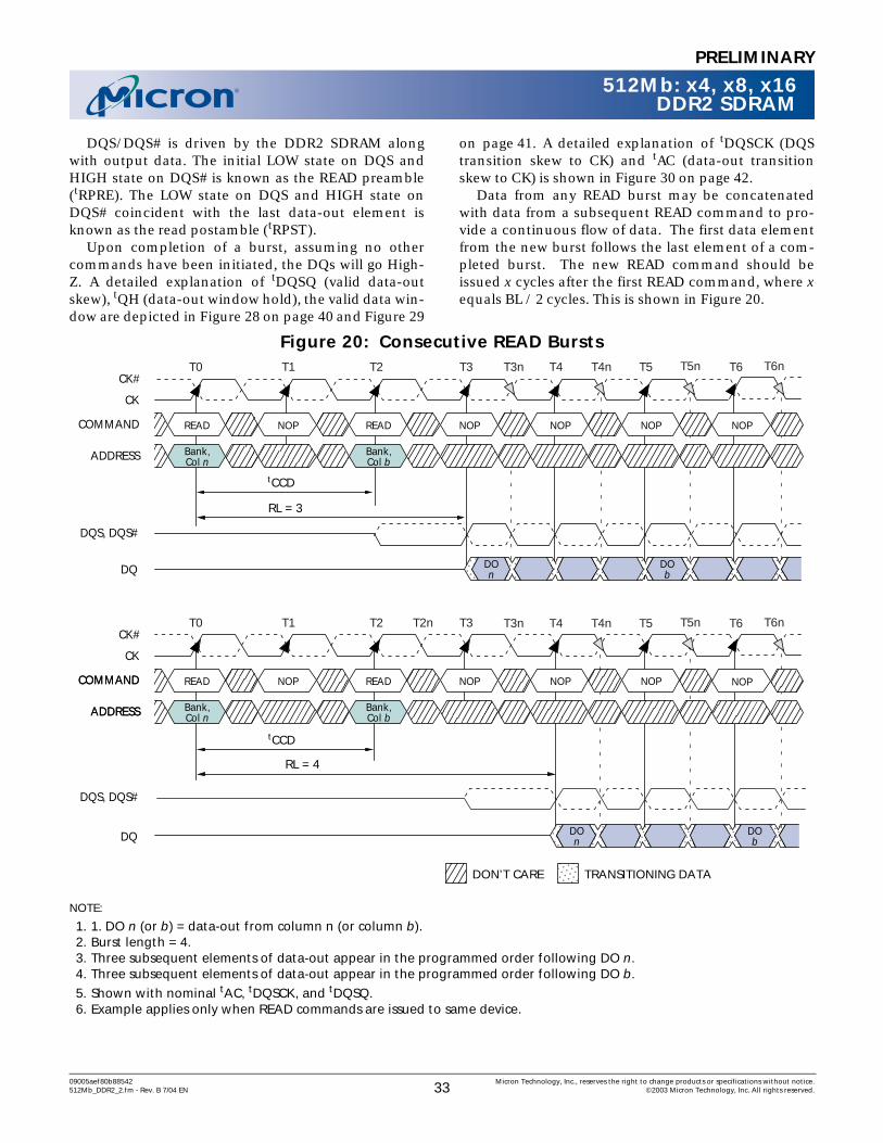
512Mb: x4, x8, x16DDR2 SDRAM
PRELIMINARY
DQS/DQS# is driven by the DDR2 SDRAM alongwith output data. The initial LOW state on DQS andHIGH state on DQS# is known as the READ preamble(tRPRE). The LOW state on DQS and HIGH state onDQS# coincident with the last data-out element isknown as the read postamble (tRPST).
Upon completion of a burst, assuming no othercommands have been initiated, the DQs will go High-Z. A detailed explanation of tDQSQ (valid data-outskew), tQH (data-out window hold), the valid data win-dow are depicted in Figure 28 on page 40 and Figure 29
on page 41. A detailed explanation of tDQSCK (DQStransition skew to CK) and tAC (data-out transitionskew to CK) is shown in Figure 30 on page 42.
Data from any READ burst may be concatenatedwith data from a subsequent READ command to pro-vide a continuous flow of data. The first data elementfrom the new burst follows the last element of a com-pleted burst. The new READ command should beissued x cycles after the first READ command, where xequals BL / 2 cycles. This is shown in Figure 20.
Figure 20: Consecutive READ Bursts
NOTE:
1. 1. DO n (or b) = data-out from column n (or column b).2. Burst length = 4.3. Three subsequent elements of data-out appear in the programmed order following DO n.4. Three subsequent elements of data-out appear in the programmed order following DO b.
5. Shown with nominal tAC, tDQSCK, and tDQSQ.6. Example applies only when READ commands are issued to same device.
CK
CK#
COMMAND READ NOP READ NOP NOP NOP NOP
ADDRESS Bank,Col n
Bank,Col b
COMMAND READ NOP READ NOP NOP NOP
ADDRESS Bank,Col n
Bank,Col b
RL = 3
CK
CK#
COMMAND
ADDRESS
DQ
DQS, DQS#
RL = 4
DQ
DQS, DQS#
DOn
DOb
DOn
DOb
T0 T1 T2 T3 T3n T4nT4 T5 T6T5n T6n
T0 T1 T2 T3T2n
NOP
T3n T4nT4 T5 T6T5n T6n
DON’T CARE TRANSITIONING DATA
tCCD
tCCD
09005aef80b88542 Micron Technology, Inc., reserves the right to change products or specifications without notice.512Mb_DDR2_2.fm - Rev. B 7/04 EN 33 ©2003 Micron Technology, Inc. All rights reserved.

512Mb: x4, x8, x16DDR2 SDRAM
PRELIMINARY
Figure 21: Nonconsecutive READ Bursts
NOTE:
1. DO n (or b) = data-out from column n (or column b).2. Burst length = 4.3. Three subsequent elements of data-out appear in the programmed order following DO n.4. Three subsequent elements of data-out appear in the programmed order following DO b.
5. Shown with nominal tAC, tDQSCK, and tDQSQ.6. Example applies when READ commands are issued to different devices or nonconsecutive READs.
Nonconsecutive read data is illustrated in Figure 21on page 34. Full-speed random read accesses within apage (or pages) can be performed. DDR2 SDRAM sup-ports the use of concurrent auto precharge timing,which is shown in Table 7 on page 36.
DDR2 SDRAM does not allow interrupting or trun-cating of any READ burst using BL = 4 operations.Once the BL = 4 READ command is registered, it mustbe allowed to complete the entire READ burst. How-
ever, a READ (with AUTO PRECHARGE disabled) usingBL = 8 operation may be interrupted and truncatedONLY by another READ burst as long as the interrup-tion occurs on a four-bit boundary due to the 4nprefetch architecture of DDR2 SDRAM. READ burst BL= 8 operations may not be interrupted or truncatedwith any command except another READ command asshown in Figure 22 on page 35.
CK
CK#
COMMAND READ NOP NOP NOP NOP NOP NOP NOP
ADDRESS Bank,Col n
READ
Bank,Col b
COMMAND
ADDRESS
CL = 3
CK
CK#
COMMAND
ADDRESS
DQ
DQS, DQS#
CL = 4
DQ
DQS, DQS#
DOn
T0 T1 T2 T3 T3n T4 T5 T7 T8T6T4n T6n T7n
NOP NOP NOP NOP
T5 T7 T8T5n T6T4n T7n
READ NOP NOP NOP
Bank,Col n
READ
Bank,Col b
T0 T1 T2 T3 T4
DOb
DOn
DOb
DON’T CARE TRANSITIONING DATA
09005aef80b88542 Micron Technology, Inc., reserves the right to change products or specifications without notice.512Mb_DDR2_2.fm - Rev. B 7/04 EN 34 ©2003 Micron Technology, Inc. All rights reserved.
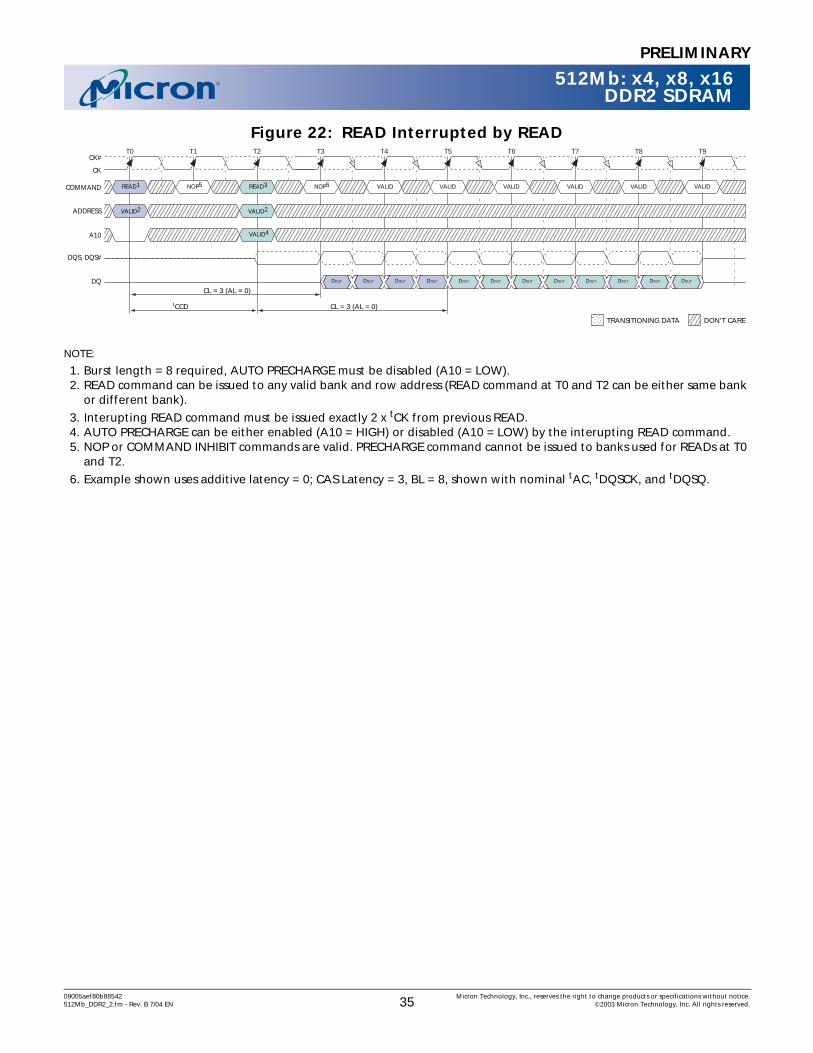
512Mb: x4, x8, x16DDR2 SDRAM
PRELIMINARY
Figure 22: READ Interrupted by READ
NOTE:
1. Burst length = 8 required, AUTO PRECHARGE must be disabled (A10 = LOW).2. READ command can be issued to any valid bank and row address (READ command at T0 and T2 can be either same bank
or different bank).
3. Interupting READ command must be issued exactly 2 x tCK from previous READ.4. AUTO PRECHARGE can be either enabled (A10 = HIGH) or disabled (A10 = LOW) by the interupting READ command.5. NOP or COMMAND INHIBIT commands are valid. PRECHARGE command cannot be issued to banks used for READs at T0
and T2.
6. Example shown uses additive latency = 0; CAS Latency = 3, BL = 8, shown with nominal tAC, tDQSCK, and tDQSQ.
DOUTDOUTDOUT
CK
CK#
COMMAND
DQ
DQS, DQS#
CL = 3 (AL = 0)
READ1
T0 T1 T2
DON’T CARETRANSITIONING DATA
NOP5 NOP5
DOUT
T3 T4 T5
VALID VALID
T6
VALIDREAD3
DOUTDOUTDOUTDOUT DOUTDOUTDOUTDOUT
VALID VALID VALID
T7 T8 T9
CL = 3 (AL = 0)tCCD
ADDRESS
A10 VALID4
VALID2VALID2
09005aef80b88542 Micron Technology, Inc., reserves the right to change products or specifications without notice.512Mb_DDR2_2.fm - Rev. B 7/04 EN 35 ©2003 Micron Technology, Inc. All rights reserved.

512Mb: x4, x8, x16DDR2 SDRAM
PRELIMINARY
Data from any READ burst must be completedbefore a subsequent WRITE burst is allowed. An exam-ple of a READ burst followed by a WRITE burst isshown in Figure 25. The tDQSS (MIN) case is shown;the tDQSS (MAX) case has a longer bus idle time.(tDQSS [MIN] and tDQSS [MAX] are defined in the sec-tion on WRITEs.)
A READ burst may be followed by a PRECHARGEcommand to the same bank provided that AUTO PRE-CHARGE is not activated. Examples of READ to PRE-CHARGE are shown in Figure 23 for BL=4 andFigure 24 for BL=8. The delay from READ command toPRECHARGE command to the same bank is AL + BL/2+ tRTP - 2 clocks.
If A10 is HIGH when a READ command is issued,the READ with AUTO PRECHARGE function isengaged. The DDR2 SDRAM starts an AUTO PRE-CHARGE operation on the rising edge which is (AL +
BL/2) cycles later than the READ with AP command iftRAS (MIN) and tRTP are satisfied. If tRAS (MIN) is notsatisfied at the edge, the start point of AUTO PRE-CHARGE operation will be delayed until tRAS (MIN) issatisfied. If tRTP (MIN) is not satisfied at the edge, thestart point of the AUTO PRECHARGE operation will bedelayed until tRTP (MIN) is satisfied. In case the inter-nal precharge is pushed out by tRTP, tRP starts at thepoint where the internal precharge happens (not at thenext rising clock edge after this event). So for BL = 4 theminimum time from READ with AP to the next activatecommand becomes AL + (tRTP + tRP)* (see Figure 23on page 36); for BL = 8 the time from READ with AP tothe next activate is AL + 2 clocks + (tRTP + tRP)* (seeFigure 24 on page 37), where * means each parameterterm is divided by tCK and rounded up to the next inte-ger. In any event, internal precharge does not start ear-lier than two clocks after the last four-bit prefetch.
Figure 23: READ to PRECHARGE BL = 4
Table 7: READ Using Concurrent Auto PrechargeBL = burst length.
FROM COMMAND(BANK n)
TO COMMAND(BANK m)
MINIMUM DELAY (WITH CONCURRENT AUTO PRECHARGE) UNITS
READ with Auto
Precharge
READ or READ w/AP (BL/2) tCKWRITE or WRITE w/AP (BL/2) + 2 tCKPRECHARGE or ACTIVE 1 tCK
DOUTDOUTDOUT
CK
CK#
COMMAND
DQ
DQS, DQS#
CL = 3
READ
Read Latency = 4 (AL = 1, CL = 3), BL = 4, tRTP ≥ 2 clocksShown with nominal tAC, tDQSCK, and tDQSQ
T0 T1 T2
DON’T CARETRANSITIONING DATA
NOP PRECHARGE
DOUT
T3 T4 T5 T6
ACTIVE
T7
ADDRESS
A10
AL=1
NOP
Bank a
≥tRTP(MIN)
Bank a
≥tRAS(MIN)
Bank a
≥tRP(MIN)
NOP NOP
AL + BL/2 + tRTP - 2 clocks
NOP
≥tRC(MIN)
4-bit prefetch
Valid Valid
09005aef80b88542 Micron Technology, Inc., reserves the right to change products or specifications without notice.512Mb_DDR2_2.fm - Rev. B 7/04 EN 36 ©2003 Micron Technology, Inc. All rights reserved.

512Mb: x4, x8, x16DDR2 SDRAM
PRELIMINARY
Figure 24: READ to PRECHARGE BL = 8
Figure 25: READ to WRITE
DOUTDOUTDOUT
CK
CK#
COMMAND
DQ
DQS, DQS#
CL = 3
READ
Read Latency = 4 (AL=1, CL=3), BL=8, tRTP ≥ 2 clocksShown with nominal tAC, tDQSCK, and tDQSQ
T0 T1 T2
DON’T CARETRANSITIONING DATA
NOP
DOUT
T3 T4 T5 T6 T7 T8
ADDRESS
A10
AL=1
NOP
Bank a
≥tRC(MIN)
≥tRTP(MIN)
NOPNOP
DOUTDOUTDOUTDOUT
first 4-bit prefetch
second 4-bit prefetch
≥tRP(MIN)
PRECHARGE
Bank a Bank a
NOP
AL + BL/2 + tRTP - 2 clocks
NOP ACTIVE
≥tRAS(MIN)
Valid Valid
DOUT
n + 3DOUT
n + 2DOUT
n + 1
CK
CK#
COMMAND
DQ
DQS, DQS#
AL = 2
ACTIVE n
Burst length = 4 Shown with nominal tAC, tDQSCK, and tDQSQ
T0 T1 T2
DON’T CARETRANSITIONING DATA
READ n NOP NOP
DOUT
n
T3 T4 T5
NOP WRITE n
T6
NOP
Din
n + 3Din
n + 2Din
n + 1
WL = RL - 1 = 4
T7 T8
NOP NOP NOP
Din
n
T9 T10 T11
NOP NOP
CL = 3
RL = 5
CAS# read latency (CL) = 3Posted CAS# additive latency (AL) = 2
tRCD = 3
09005aef80b88542 Micron Technology, Inc., reserves the right to change products or specifications without notice.512Mb_DDR2_2.fm - Rev. B 7/04 EN 37 ©2003 Micron Technology, Inc. All rights reserved.

512Mb: x4, x8, x16DDR2 SDRAM
PRELIMINARY
Figure 26: Bank Read – Without Auto Precharge
NOTE:
1. DO n = data-out from column n; subsequent elements are applied in the programmed order.2. Burst length = 4 and AL = 0 in the case shown.3. Disable auto precharge.4. “Don’t Care” if A10 is HIGH at T5.5. PRE = PRECHARGE, ACT = ACTIVE, RA = row address, BA = bank address.6. NOP commands are shown for ease of illustration; other commands may be valid at these times.
7. The PRECHARGE command can only be applied at T6 if tRAS minimum is met.
8. Read to Precharge = AL +BL/2 + tRTP-2 clocks.9. I/0 pins, when entering or exiting HIGH-Z are not referenced to a specific voltage level, but when the device begins to
drive or no longer drives, respecively.
CK
CK#
CKE
A10
BA0, BA1
tCK tCH tCL
RA
tRCD
tRAS7
tRC
tRP
CL = 3
DM
T0 T1 T2 T3 T4 T5 T7n T8nT6 T7 T8
DQ1
DQS, DQS#
Case 1: tAC (MIN) and tDQSCK (MIN)
Case 2: tAC (MAX) and tDQSCK (MAX)
DQ1
DQS, DQS#
tRPRE
tRPRE
tRPST
tRPST
tDQSCK (MIN)
tDQSCK (MAX)
tLZ (MIN)
tLZ (MAX)
tAC (MIN)tLZ (MIN)
DOn
tHZ (MAX)tAC (MAX)tLZ (MIN)
DOn
NOP6NOP6COMMAND5 ACT
RA Col n
PRE7
Bank x
RA
RA
Bank xBank x4
99
9 9
ACT
Bank x
NOP6 NOP6 NOP6 NOP6
tHZ (MIN)
ONE BANK
ALL BANKS
DON’T CARE TRANSITIONING DATA
READ2
ADDRESS
3
tRTP 8
09005aef80b88542 Micron Technology, Inc., reserves the right to change products or specifications without notice.512Mb_DDR2_2.fm - Rev. B 7/04 EN 38 ©2003 Micron Technology, Inc. All rights reserved.

512Mb: x4, x8, x16DDR2 SDRAM
PRELIMINARY
Figure 27: Bank Read – With Auto Precharge
NOTE:
1. DO n = data-out from column n; subsequent elements are applied in the programmed order.2. Burst length = 4, RL = 4 (AL = 1, CL = 3) in the case shown.3. Enable auto precharge.4. ACT = ACTIVE, RA = row address, BA = bank address.5. NOP commands are shown for ease of illustration; other commands may be valid at these times.
6. The DDR2 SDRAM internally delays auto precharge until both tRAS (MIN) and tRTP (MIN) have been satisfied.7. I/0 pins, when entering or exiting HIGH-Z are not referenced to a specific voltage level, but when the device begins to
drive or no longer drives, respecively.
CK
CK#
CKE
A10
BA0, BA1
tCK tCH tCL
RA
tRCD
tRAS
tRC
tRP
CL = 3
DM
T0 T1 T2 T3 T4 T5 T7n T8nT6 T7 T8
DQ1
DQS,DQS#
Case 1: tAC (MIN) and tDQSCK (MIN)
Case 2: tAC (MAX) and tDQSCK (MAX)
DQ1
DQS, DQS#
tRPRE
tRPRE
tRPST
tRPST
tDQSCK (MIN)
tDQSCK (MAX)
tLZ (MIN)
tLZ (MAX)
tAC (MIN)tLZ (MIN)
DOn
tHZ (MAX)tAC (MAX)tLZ (MAX)
DOn
NOP5NOP5COMMAND5 ACT
RA Col n
Bank x
RA
RA
Bank x
ACT
Bank x
NOP5 NOP5 NOP5 NOP5 NOP5
tHZ (MIN)
DON’T CARE
TRANSITIONING DATA
READ2,6
ADDRESS
AL=1
4-bitprefetch
tRTP
Internalprecharge
3
77
7 7
09005aef80b88542 Micron Technology, Inc., reserves the right to change products or specifications without notice.512Mb_DDR2_2.fm - Rev. B 7/04 EN 39 ©2003 Micron Technology, Inc. All rights reserved.

512Mb: x4, x8, x16DDR2 SDRAM
PRELIMINARY
Figure 28: x4, x8 Data Output Timing – tDQSQ, tQH, and Data Valid Window
NOTE:
1. DQs transitioning after DQS transition define tDQSQ window. DQS transitions at T2 and at T2n are “early DQS,” at T3 are “nominal DQS,” and at T3n are "late DQS."
2. For a x4, only two DQs apply.
3. tDQSQ is derived at each DQS clock edge and is not cumulative over time and begins with DQS transitions and ends with the last valid transition of DQs .
4. tQH is derived from tHP: tQH = tHP - tQHS.
5. tHP is the lesser of tCL or tCH clock transitions collectively when a bank is active.
6. The data valid window is derived for each DQS transition and is defined as tQH minus tDQSQ.
DQ (Last data valid)DQ2
DQ2
DQ2
DQ2
DQ2
DQ2
DQS#DQS1
DQ (Last data valid)
DQ (First data no longer valid)
DQ (First data no longer valid)
All DQs and DQS, collectively6
Earliest signal transition
Latest signal transition
T2
T2
T2
T2n
T2n
T2n
T3
T3
T3
T3n
T3n
T3n
CKCK#
T1 T2 T3 T4T2n T3n
tQH4
tHP5 tHP5 tHP5
tQH4 tQH4
tHP5tHP5 tHP5
tQH4
tDQSQ3 tDQSQ3 tDQSQ3 tDQSQ3
DataValid
window
DataValid
window
DataValid
window
DataValid
window
09005aef80b88542 Micron Technology, Inc., reserves the right to change products or specifications without notice.512Mb_DDR2_2.fm - Rev. B 7/04 EN 40 ©2003 Micron Technology, Inc. All rights reserved.

512Mb: x4, x8, x16DDR2 SDRAM
PRELIMINARY
Figure 29: x16 Data Output Timing – tDQSQ, tQH, and Data Valid Window
NOTE:
1. DQs transitioning after DQS transitions define the tDQSQ window. LDQS defines the lower byte, and UDQS defines the upper byte.
2. DQ0, DQ1, DQ2, DQ3, DQ4, DQ5, DQ6, or DQ7.
3. tDQSQ is derived at each DQS clock edge and is not cumulative over time and begins with DQS transitions and ends with the last valid transition of DQs.
4. tQH is derived from tHP: tQH = tHP - tQHS.
5. tHP is the lesser of tCL or tCH clock transitions collectively when a bank is active.
6. The data valid window is derived for each DQS transition and is tQH minus tDQSQ.7. DQ8, DQ9, DQ10, D11, DQ12, DQ13, DQ14, or DQ15.
DQ (Last data valid)2
DQ2
DQ2
DQ2
DQ2
DQ2
DQ2
LDSQ#LDQS1
DQ (Last data valid)2
DQ (First data no longer valid)2
DQ (First data no longer valid)2
DQ0–DQ7 and LDQS, collectively6 T2
T2
T2
T2n
T2n
T2n
T3
T3
T3
T3n
T3n
T3n
CKCK#
T1 T2 T3 T4T2n T3n
tQH4 tQH4
tDQSQ3 tDQSQ3 tDQSQ3 tDQSQ3
Data Valid window
Data Valid window
DQ (Last data valid)7
DQ7
DQ7
DQ7
DQ7
DQ7
DQ7
UDQS#UDQS1
DQ (Last data valid)7
DQ (First data no longer valid)7
DQ (First data no longer valid)7
DQ8–DQ15 and UDQS, collectively6 T2
T2
T2
T2n
T2n
T2n
T3
T3
T3
T3n
T3n
T3n
tQH4tQH4 tQH4 tQH4
tDQSQ3 tDQSQ3 tDQSQ3tDQSQ3
tHP5 tHP5 tHP5 tHP5tHP5tHP5
tQH4tQH4
Data Valid window
Data Valid window
Data Valid window
Data Valid window
Data Valid window
Up
per B
yteLo
wer B
yte
Data Valid window
09005aef80b88542 Micron Technology, Inc., reserves the right to change products or specifications without notice.512Mb_DDR2_2.fm - Rev. B 7/04 EN 41 ©2003 Micron Technology, Inc. All rights reserved.

512Mb: x4, x8, x16DDR2 SDRAM
PRELIMINARY
Figure 30: Data Output Timing – tAC and tDQSCK
NOTE:
1. tDQSCK is the DQS output window relative to CK and is the“long-term” component of DQS skew.
2. DQs transitioning after DQS transitions define tDQSQ window.
3. All DQs must transition by tDQSQ after DQS transitions, regardless of tAC.
4. tAC is the DQ output window relative to CK and is the“long term” component of DQ skew.
5. tLZ (MIN) and tAC (MIN) are the first valid signal transitions.
6. tHZ (MAX) and tAC (MAX) are the latest valid signal transitions.7. READ command with CL=3, AL=0 issued at T0.8. I/0 pins, when entering or exiting HIGH-Z are not referenced to a specific voltage level, but when the device begins to
drive or no longer drives, respecively.
CK
CK#
DQS#/DQS, or LDQS#/LDQS / UDQ#/UDQS2
T07 T1 T2 T3 T3n T4 T4n T5 T5n T6 T6n T7
tRPST
tLZ (MIN)
tDQSCK1 (MAX)tDQSCK1 (MIN)
tDQSCK1 (MAX)tDQSCK1 (MIN)
tHZ (MAX)
tRPRE
DQ (Last data valid)
DQ (First data valid)
All DQs collectively3
tAC4 (MIN) tAC4 (MAX)tLZ (MIN) tHZ (MAX)
T3
T3
T3n T4n T5n T6n
T3n
T3n
T4n
T4n
T5n
T5n
T6n
T6n
T4
T5
T5
T6
T6
T3 T4 T5 T6
T4
09005aef80b88542 Micron Technology, Inc., reserves the right to change products or specifications without notice.512Mb_DDR2_2.fm - Rev. B 7/04 EN 42 ©2003 Micron Technology, Inc. All rights reserved.

512Mb: x4, x8, x16DDR2 SDRAM
PRELIMINARY
WRITEs
WRITE CommandThe WRITE command is used to initiate a burst
write access to an active row. The value on the BA1-BA0 inputs selects the bank, and the address providedon inputs A0–i (where i = A9 for x8 and x16; or A9, A11for x4) selects the starting column location. The valueon input A10 determines whether or not auto pre-charge is used. If auto precharge is selected, the rowbeing accessed will be precharged at the end of thewrite burst; if auto precharge is not selected, the rowwill remain open for subsequent accesses.
Figure 31: WRITE Command
Input data appearing on the DQs is written to thememory array subject to the DM input logic levelappearing coincident with the data. If a given DM sig-nal is registered LOW, the corresponding data will bewritten to memory; if the DM signal is registeredHIGH, the corresponding data inputs will be ignored,and a write will not be executed to that byte/columnlocation (Figure 41).
WRITE OperationWRITE bursts are initiated with a WRITE command,
as shown in Figure 31. DDR2 SDRAM uses WriteLatency (WL) equal to Read Latency minus 1 clockcycle (WL = RL - 1 = AL + CL - 1). The starting columnand bank addresses are provided with the WRITE com-mand, and auto precharge is either enabled or dis-abled for that access. If auto precharge is enabled, therow being accessed is precharged at the completion ofthe burst. For the generic WRITE commands used inthe following illustrations, auto precharge is disabled.
During WRITE bursts, the first valid data-in elementwill be registered on the first rising edge of DQS follow-ing the WRITE command, and subsequent data ele-ments will be registered on successive edges of DQS.The LOW state on DQS between the WRITE commandand the first rising edge is known as the write pream-ble; the LOW state on DQS following the last data-inelement is known as the write postamble.
The time between the WRITE command and thefirst corresponding rising edge of DQS (tDQSS) is spec-ified with a relatively wide range (from 75 percent to125 percent of one clock cycle). All of the WRITE dia-grams show the nominal case, and where the twoextreme cases (i.e., tDQSS [MIN] and tDQSS [MAX])might not be intuitive, they have also been included.Figure 32 shows the nominal case and the extremes oftDQSS for a burst of 4. Upon completion of a burst,assuming no other commands have been initiated, theDQs will remain High-Z and any additional input datawill be ignored.
Data for any WRITE burst may be concatenatedwith a subsequent WRITE command to provide con-tinuous flow of input data. The first data element fromthe new burst is applied after the last element of acompleted burst. The new WRITE command should beissued x cycles after the first WRITE command, wherex equals BL/2.
Figure 33 shows concatenated bursts of 4. An exam-ple of nonconsecutive WRITEs is shown in Figure 34.Full-speed random write accesses within a page orpages can be performed as shown in Figure 35. DDR2SDRAM supports concurrent auto precharge optionsshown in Table 8.
DDR2 SDRAM does not allow interrupting or trun-cating any WRITE burst using BL = 4 operation. Oncethe BL = 4 WRITE command is registered, it must beallowed to complete the entire WRITE burst cycle.However, a WRITE (with AUTO PRECHARGE disabled)using BL = 8 operations may be interrupted and trun-
CS#
WE#
CAS#
RAS#
CKE
CA
A10
BANK ADDRESS
HIGH
EN AP
DIS AP
BA
CK
CK#
CA = column addressBA = bank addressEN AP = enable auto prechargeDIS AP = disable auto precharge
DON’T CARE
ADDRESS
09005aef80b88542 Micron Technology, Inc., reserves the right to change products or specifications without notice.512Mb_DDR2_2.fm - Rev. B 7/04 EN 43 ©2003 Micron Technology, Inc. All rights reserved.

512Mb: x4, x8, x16DDR2 SDRAM
PRELIMINARY
cated ONLY by another WRITE burst as long as theinterruption occurs on a four-bit boundary due to the4n prefetch architecture of DDR2 SDRAM. WRITEburst BL = 8 operations may NOT be interrupted ortruncated with any command except another WRITEcommand as shown in Figure 36.
Data for any WRITE burst may be followed by a sub-sequent READ command. To follow a WRITE tWTRshould be met as shown in Figure 37. tWTR is defined
as Min(2 or tWTR/tCK rounded up to the next integer).Data for any WRITE burst may be followed by a subse-quent PRECHARGE command. tWR must be met asshown in Figure 31. tWR starts at the end of the databurst regardless of the data mask condition.
Table 8: WRITE Using Concurrent Auto PrechargeCL = CAS latency, BL = burst length
FROM COMMAND(BANK n)
TO COMMAND(BANK m)
MINIMUM DELAY (WITH CONCURRENT AUTO PRECHARGE) UNITS
WRITE with Auto
Precharge
READ or READ w/AP (CL-1) + (BL/2) + tWTR tCKWRITE or WRITE w/AP (BL/2) tCKPRECHARGE or ACTIVE 1 tCK
09005aef80b88542 Micron Technology, Inc., reserves the right to change products or specifications without notice.512Mb_DDR2_2.fm - Rev. B 7/04 EN 44 ©2003 Micron Technology, Inc. All rights reserved.

512Mb: x4, x8, x16DDR2 SDRAM
PRELIMINARY
Figure 32: WRITE Burst
NOTE:
1. DI b = data-in for column b.2. Three subsequent elements of data-in are applied in the programmed order following DI b.3. A burst of 4 is shown with AL = 0, CL = 3; thus, WL = 2.4. A10 is LOW with the WRITE command (auto precharge is disabled).
5. Subsequent rising DQS signals must align to the clock within ±0.25 tck
DQS, DQS#
tDQSS (MAX)
tDQSS (NOM)
tDQSS (MIN)
tDQSS
DM
DQ
CK
CK#
COMMAND WRITE NOP NOP
ADDRESS Bank a,Col b
NOP NOP
T0 T1 T2 T3T2n T4T3n
DQS, DQS#
tDQSS
5
5
5
DM
DQ
DQS, DQS#
tDQSS
DM
DQ DIb
DIb
DIb
DON’T CARE TRANSITIONING DATA
09005aef80b88542 Micron Technology, Inc., reserves the right to change products or specifications without notice.512Mb_DDR2_2.fm - Rev. B 7/04 EN 45 ©2003 Micron Technology, Inc. All rights reserved.

512Mb: x4, x8, x16DDR2 SDRAM
PRELIMINARY
Figure 33: Consecutive WRITE to WRITE
NOTE:
1. DI b, etc. = data-in for column b, etc.2. Three subsequent elements of data-in are applied in the programmed order following DI b.3. Three subsequent elements of data-in are applied in the programmed order following DI n.4. A burst of 4 is shown with AL = 0, CL = 3; thus, WL = 2.5. Each WRITE command may be to any bank.
6. Subsequent rising DQS signals must align to the clock within ±0.25 tck
Figure 34: Nonconsecutive WRITE to WRITE
NOTE:
1. DI b, etc. = data-in for column b, etc.2. Three subsequent elements of data-in are applied in the programmed order following DI b.3. Three subsequent elements of data-in are applied in the programmed order following DI n.4. A burst of 4 is shown. AL = 0, CL = 3; thus, WL = 2.5. Each WRITE command may be to any bank.
6. Subsequent rising DQS signals must align to the clock within ±0.25 tck
CK
CK#
COMMAND WRITE NOP WRITE NOP NOP NOP
ADDRESS Bank,Col b
NOP
Bank,Col n
T0 T1 T2 T3T2n T4 T5T4n T6T5nT3nT1n
DQ
DQS, DQS#
DM
DIn
DIb
DON’T CARE TRANSITIONING DATA
tDQSStDQSS (NOM)
WL = 2
tCCD
WL = 2
6
CK
CK#
COMMAND WRITE NOP NOP NOP NOP NOP
ADDRESS Bank,Col b
WRITE
Bank,Col n
T0 T1 T2 T3T2n T4 T5T4nT3n T5n T6 T6n
DQ
DQS, DQS#
DM
DIn
DIb
tDQSS (NOM) tDQSS
DON’T CARE TRANSITIONING DATA
WL = 2 WL = 2
6
09005aef80b88542 Micron Technology, Inc., reserves the right to change products or specifications without notice.512Mb_DDR2_2.fm - Rev. B 7/04 EN 46 ©2003 Micron Technology, Inc. All rights reserved.

512Mb: x4, x8, x16DDR2 SDRAM
PRELIMINARY
Figure 35: Random WRITE Cycles
NOTE:
1. DI b, etc. = data-in for column b, etc.2. Three subsequent elements of data-in are applied in the programmed order following DI b.3. Three subsequent elements of data-in are applied in the programmed order following DI n.4. An burst of 4 is shown. AL = 0, CL = 3; thus, WL = 2.5. Each WRITE command may be to any bank.
6. Subsequent rising DQS signals must align to the clock within ±0.25 tck
Figure 36: WRITE Interrupted by WRITE
NOTE:
1. Burst length = 8 required, AUTO PRECHARGE must be disabled (A10 = LOW).2. WRITE command can be issued to any valid bank and row address (WRITE command at T0 and T2 can be either same
bank or different bank).
3. Interupting WRITE command must be issued exactly 2 x tCK from previous WRITE.4. AUTO PRECHARGE can be either enabled (A10 = HIGH) or disabled (A10 = LOW) by the interupting WRITE command.5. NOP or COMMAND INHIBIT commands are valid. PRECHARGE command can not be issued to banks used for WRITEs at
T0 and T2.
6. Earliest WRITE-to-PRECHARGE timing for WRITE at T0 is WL + BL/2 + tWR where tWR starts with T7 and not T5 (since BL = 8 from MR and not the truncated length).
7. Example shown uses Additive Latency = 0; CAS Latency = 4, BL = 8.
8. Subsequent rising DQS signals must align to the clock within ±0.25 tck
CK
CK#
COMMAND WRITE NOP WRITE NOP NOP NOP
ADDRESS Bank,Col b
NOP
Bank,Col n
T0 T1 T2 T3T2n T4 T5T4n T6T5nT3nT1n
DQ
DQS, DQS#
DM
DIn
DIb
DON’T CARE TRANSITIONING DATA
tDQSStDQSS (NOM)
WL = 2
tCCD
WL = 2
6
DIN
a + 3DIN
a + 2DIN
a + 1
CK
CK#
COMMAND
DQ
DQS, DQS#
WL = 3
WRITE1a
T0 T1 T2
DON’T CARETRANSITIONING DATA
DIN a
T3 T4 T5 T6
WRITE3b
DIN
b + 3DIN
b + 2DIN
b + 1DIN
bDIN
b + 7DIN
b + 6DIN
b + 5DIN
b + 4
T7 T8 T9
WL = 32 clock requirement
ADDRESS
A10 VALID4
VALID2 VALID2
VALID6 VALID6 VALID6NOP5NOP5NOP5NOP5NOP5
8
09005aef80b88542 Micron Technology, Inc., reserves the right to change products or specifications without notice.512Mb_DDR2_2.fm - Rev. B 7/04 EN 47 ©2003 Micron Technology, Inc. All rights reserved.

512Mb: x4, x8, x16DDR2 SDRAM
PRELIMINARY
Figure 37: WRITE to READ
NOTE:
1. DI b = data-in for column b; Dout n = data out from column n.2. A burst of 4 is shown; AL = 0, CL = 3; thus, WL = 2.3. One subsequent element of data-in is applied in the programmed order following DI b.
4. tWTR is referenced from the first positive CK edge after the last data-in pair.5. A10 is LOW with the WRITE command (auto precharge is disabled).
6. tWTR is defined as Min(2 or tWTR/tCK rounded up to the next integer).7. Required for any READ following a WRITE to the same device.
8. Subsequent rising DQS signals must align to the clock within ±0.25 tck
tDQSS (NOM)
CK
CK#
COMMAND WRITE NOP NOP NOP NOP NOP NOP NOP
ADDRESS Bank a,Col b
Bank a,Col n
READ
T0 T1 T2 T3T2n T4 T5 T9nT3n T6 T7 T8 T9
tWTR7
CL = 3
CL = 3
CL = 3
DQ
DQS, DQS#
DM
DIb
tDQSS (MIN)
DQ
DQS, DQS#
DM
DIb
tDQSS (MAX)
DQ
DQS, DQS#
DM
DIb Dout
Dout
DON’T CARE TRANSITIONING DATA
tDQSS
tDQSS
tDQSS
NOP
Dout
8
8
8
09005aef80b88542 Micron Technology, Inc., reserves the right to change products or specifications without notice.512Mb_DDR2_2.fm - Rev. B 7/04 EN 48 ©2003 Micron Technology, Inc. All rights reserved.

512Mb: x4, x8, x16DDR2 SDRAM
PRELIMINARY
Figure 38: WRITE to PRECHARGE
NOTE:
1. DI b = data-in for column b.2. Three subsequent elements of data-in are applied in the programmed order following DI b.3. BL=4; CL = 3; AL = 0; thus, WL = 2.
4. tWR is referenced from the first positive CK edge after the last data-in pair.5. The PRECHARGE and WRITE commands are to the same bank. However, the PRECHARGE and WRITE commands may be
to different banks, in which case tWR is not required and the PRECHARGE command could be applied earlier.6. A10 is LOW with the WRITE command (auto precharge is disabled).7. PRE = PRECHARGE command.
8. Subsequent rising DQS signals must align to the clock within ±0.25 tck
tDQSS (NOM)
CK
CK#
COMMAND WRITE NOP NOP NOP NOPNOP
ADDRESS Bank a,Col b
Bank,(a or all)
NOP
T0 T1 T2 T3T2n T4 T5T3n T6 T7
tWR tRP
DQ
DQS#DQS
DM
DIb
tDQSS (MIN)
DQ
DQS#DQS
DM
DIb
tDQSS (MAX)
DQ
DQS#DQS
DM
DIb
DON’T CARE TRANSITIONING DATA
tDQSS
tDQSS
tDQSS
PRE7
8
8
8
09005aef80b88542 Micron Technology, Inc., reserves the right to change products or specifications without notice.512Mb_DDR2_2.fm - Rev. B 7/04 EN 49 ©2003 Micron Technology, Inc. All rights reserved.

512Mb: x4, x8, x16DDR2 SDRAM
PRELIMINARY
Figure 39: Bank Write–Without Auto Precharge
NOTE:
1. DI n = data-in from column n; subsequent elements are applied in the programmed order.2. BL = 4, AL = 0, and WL = 2 in the case shown.3. Disable auto precharge.4. “Don’t Care” if A10 is HIGH at T9.5. PRE = PRECHARGE, ACT = ACTIVE, RA = row address, BA = bank address.6. NOP commands are shown for ease of illustration; other commands may be valid at these times.
7. tDSH is applicable during tDQSS (MIN) and is referenced from CK T5 or T6.
8. tDSS is applicable during tDQSS (MAX) and is referenced from CK T6 or T7.
9. Subsequent rising DQS signals must align to the clock within ±0.25 tck
CK
CK#
CKE
A10
BA0, BA1
tCK tCH tCL
RA
tRCD
tRAS tRP
tWR
T0 T1 T2 T3 T5 T6 T6n T7 T8 T9T5n
NOP6NOP6COMMAND5
3
9
ACT
RA Col n
WRITE2 NOP6
ONE BANK
ALL BANKS
Bank x
PRE
Bank x
NOP6 NOP6 NOP6
tDQSL tDQSH tWPST
Bank x4
DQ1
DM
DIn
DON’T CARE TRANSITIONING DATA
tDQSS (NOM)
tWPRE
DQS, DQS#
ADDRESS
NOP6
WL=2
T4
09005aef80b88542 Micron Technology, Inc., reserves the right to change products or specifications without notice.512Mb_DDR2_2.fm - Rev. B 7/04 EN 50 ©2003 Micron Technology, Inc. All rights reserved.

512Mb: x4, x8, x16DDR2 SDRAM
PRELIMINARY
Figure 40: Bank Write–with Auto Precharge
NOTE:
1. DI n = data-in from column n; subsequent elements are applied in the programmed order.2. Burst length = 4, AL = 0, and WL = 2 shown.3. Enable auto precharge.4. ACT = ACTIVE, RA = row address, BA = bank address.5. NOP commands are shown for ease of illustration; other commands may be valid at these times.
6. tDSH is applicable during tDQSS (MIN) and is referenced from CK T5 or T6.
7. tDSS is applicable during tDQSS (MAX) and is referenced from CK T6 or T7.
8. WR is programmed via MR[11,10,9] and is calculated by dividing tWR(ns) by tCK and rounding up to the next integer value.
9. Subsequent rising DQS signals must align to the clock within ±0.25 tck
CK
CK#
CKE
A10
BA0, BA1
tCK tCH tCL
RA
tRCD
tRAS tRP
WR8
T0 T1 T2 T3 T4 T5 T5n T6 T7 T8T6n
NOP5NOP5COMMAND4
3
ACT
RA Col n
WRITE2 NOP5
Bank x
NOP5
Bank x
NOP5 NOP5 NOP5
tDQSL tDQSH tWPST
DQ1
DM
tDQSS (NOM)
DON’T CARETRANSITIONING DATA
tWPRE
DQS,DQS#
ADDRESS
T9
NOP5
WL = 2
DIn
9
09005aef80b88542 Micron Technology, Inc., reserves the right to change products or specifications without notice.512Mb_DDR2_2.fm - Rev. B 7/04 EN 51 ©2003 Micron Technology, Inc. All rights reserved.

512Mb: x4, x8, x16DDR2 SDRAM
PRELIMINARY
Figure 41: WRITE–DM Operation
NOTE:
1. DI n = data-in from column n; subsequent elements are applied in the programmed order.2. Burst length = 4, AL = 1, and WL = 2 in the case shown.3. Disable auto precharge.4. “Don’t Care” if A10 is HIGH at T11.5. PRE = PRECHARGE, ACT = ACTIVE, RA = row address, BA = bank address.6. NOP commands are shown for ease of illustration; other commands may be valid at these times.
7. tDSH is applicable during tDQSS (MIN) and is referenced from CK T6 or T7.
8. tDSS is applicable during tDQSS (MAX) and is referenced from CK T7 or T8.
9. tWR starts at the end of the data burst regardless of the data mask condition.
10. Subsequent rising DQS signals must align to the clock within ±0.25 tck
CK
CK#
CKE
A10
BA0, BA1
tCK tCH tCL
RA
tRCD
tRAS tRPA
tWR9
T0 T1 T2 T3 T4 T5 T7nT6 T7 T8T6n
NOP6NOP6COMMAND5
3
ACT
RA Col n
WRITE2 NOP6
ONE BANK
ALL BANKS
Bank xBank x
NOP6 NOP6 NOP6 NOP6 NOP6 NOP6
tDQSL tDQSH tWPST
Bank x4
DQ1
DM
DON’T CARETRANSITIONING DATA
tDQSS (NOM)
tWPRE
PRE
DQS, DQS#
ADDRESS
T9 T10 T11
AL=1 WL=2
DIn
10
09005aef80b88542 Micron Technology, Inc., reserves the right to change products or specifications without notice.512Mb_DDR2_2.fm - Rev. B 7/04 EN 52 ©2003 Micron Technology, Inc. All rights reserved.

512Mb: x4, x8, x16DDR2 SDRAM
PRELIMINARY
Figure 42: Data Input Timing
NOTE:
1. tDSH (MIN) generally occurs during tDQSS (MIN).
2. tDSS (MIN) generally occurs during tDQSS (MAX).3. WRITE command issued at T0.4. For x16, LDQS controls the lower byte and UDQS controls the upper byte.5. WRITE command with WL=2 (CL=3, AL=0) issued at T0.
6. Subsequent rising DQS signals must align to the clock within ±0.25 tck
DQS#DQS
tDQSS(nominal)
tDQSH tWPSTtDQSL
tDSS2 tDSH1tDSH1 tDSS2
DM
DQ
CK
CK#T1T0 T1n T2 T2n T3 T4T3n
DI
DON’T CARETRANSITIONING DATA
tWPRE
6
09005aef80b88542 Micron Technology, Inc., reserves the right to change products or specifications without notice.512Mb_DDR2_2.fm - Rev. B 7/04 EN 53 ©2003 Micron Technology, Inc. All rights reserved.

512Mb: x4, x8, x16DDR2 SDRAM
PRELIMINARY
Precharge
PRECHARGE CommandThe PRECHARGE command, illustrated in
Figure 43, is used to deactivate the open row in a par-ticular bank or the open row in all banks. The bank(s)will be available for a subsequent row activation aspecified time (tRP) after the precharge command isissued, except in the case of concurrent auto pre-charge, where a READ or WRITE command to a differ-ent bank is allowed as long as it does not interrupt thedata transfer in the current bank and does not violateany other timing parameters. Once a bank has beenprecharged, it is in the idle state and must be activatedprior to any READ or WRITE commands being issuedto that bank. A PRECHARGE command will be treatedas a NOP if there is no open row in that bank (idlestate) or if the previously open row is already in theprocess of precharging.
PRECHARGE OperationInput A10 determines whether one or all banks are
to be precharged, and in the case where only one bankis to be precharged, inputs BA1-BA0 select the bank.Otherwise BA1-BA0 are treated as “Don’t Care.”
When all banks are to be precharged, inputs BA1-BA0 are treated as “Don’t Care.” Once a bank has beenprecharged, it is in the idle state and must be activatedprior to any READ or WRITE commands being issuedto that bank. tRPA timing applies when the PRE-CHARGE(ALL) command is issued, regardless of thenumber of banks already open or closed. If a single-bank PRECHARGE command is issued, tRP timingapplies.
Figure 43: PRECHARGE Command
CS#
WE#
CAS#
RAS#
CKE
A10
BA0, BA1
HIGH
ALL BANKS
ONE BANK
BA
ADDRESS
CK
CK#
BA = bank address (if A10 is LOW;otherwise “Don’t Care”)
DON’T CARE
09005aef80b88542 Micron Technology, Inc., reserves the right to change products or specifications without notice.512Mb_DDR2_2.fm - Rev. B 7/04 EN 54 ©2003 Micron Technology, Inc. All rights reserved.

512Mb: x4, x8, x16DDR2 SDRAM
PRELIMINARY
Self Refresh
SELF REFRESH CommandThe SELF REFRESH command can be used to retain
data in the DDR2 SDRAM, even if the rest of the systemis powered down. When in the self refresh mode, theDDR2 SDRAM retains data without external clocking.All power supply inputs (including VREF ) must bemaintained at valid levels upon entry/exit AND duringself refresh operation.
The SELF REFRESH command is initiated like aREFRESH command except CKE is (LOW). The DLL isautomatically disabled upon entering self refresh andis automatically enabled upon exiting self refresh (200clock cycles must then occur before a READ commandcan be issued). Clock should remain stable and meet-
ing tCKE specifications at least 1 x tCK after enteringself refresh mode. All command and address input sig-nals except CKE are “Don’t Care” during self refresh.
The procedure for exiting self refresh requires asequence of commands. First, CK, CK# must be stableand meeting tCK specifications at least 1 x tCK prior toCKE going back HIGH. Once CKE is HIGH (tCKE(min)has been satified with four clock registrations), theDDR2 SDRAM must have NOP or DESELECT com-mands issued for tXSNR because time is required forthe completion of any internal refresh in progress. Asimple algorithm for meeting both refresh and DLLrequirements is to apply NOP or DESELECT com-mands for 200 clock cycles before applying any othercommand.
09005aef80b88542 Micron Technology, Inc., reserves the right to change products or specifications without notice.512Mb_DDR2_2.fm - Rev. B 7/04 EN 55 ©2003 Micron Technology, Inc. All rights reserved.

512Mb: x4, x8, x16DDR2 SDRAM
PRELIMINARY
Figure 44: Self Refresh
NOTE:
1. Clock must be stable and meeting tCK specifications at least 1 x tCK after entering self refresh and at least 1 x tCK prior to exiting self refresh mode.
2. Device must be in the all banks idle state prior to entering self refresh mode.
3. tXSNR is required before any non-READ command can be applied.
4. tXSRD (200 cycles of CK) is required before a READ command can be applied at state Td0.5. REF = REFRESH command.
6. Self Refresh exit is asynchronous, however, tXSNR and tXSRD timing starts at the first rising clock edge where CKE HIGH
satisfies tISXR.7. NOP or DESELECT commands are required prior to exiting SELF REFRESH until state Tc0, which allows any non-READ
command.
8. ODT must be disabled and RTT off (tAOFD and tAOFPD have been satisfied) prior to entering Self Refresh at state T1.
9. Once Self Refresh has been entered tCKE(min) must be satisfied prior to exiting self refresh.
10. CKE must stay high; tCKE(min) High = 3 clock registrations.
CK1
CK#
COMMAND5 NOP REF
ADDRESS
CKE1
VALID
DQ
DM
DQS#,DQS
NOP7
tRP2
tCH tCLtCK1tCK1
tXSNR3,6
tISXR6
Enter Self Refresh Mode (synchronous)
Exit Self RefreshMode (asynchronous)
T0 T1 Ta2Ta1
DON’T CARE
Ta0 Tc0Tb0
tXSRD4,6
VALID3
tCKE (MIN)10
NOP7
tCKE (MIN)9
T2
ODT8
tAOFD / tAOFPD8
8
Td0
VALID4
8
VALID3
Indicates a break in time scale
09005aef80b88542 Micron Technology, Inc., reserves the right to change products or specifications without notice.512Mb_DDR2_2.fm - Rev. B 7/04 EN 56 ©2003 Micron Technology, Inc. All rights reserved.

512Mb: x4, x8, x16DDR2 SDRAM
PRELIMINARY
REFRESH
REFRESH CommandREFRESH is used during normal operation of the
DDR2 SDRAM and is analogous to CAS#-BEFORE-RAS# (CBR) refresh. This command is nonpersistent,so it must be issued each time a refresh is required.The addressing is generated by the internal refreshcontroller. This makes the address bits a “Don’t Care”during an REFRESH command. The 512Mb DDR2SDRAM requires REFRESH cycles at an average inter-val of 7.8125µs (maximum). To allow for improved effi-
ciency in scheduling and switching between tasks,some flexibility in the absolute refresh interval is pro-vided. A maximum of eight REFRESH commands canbe posted to any given DDR2 SDRAM, meaning thatthe maximum absolute interval between anyREFRESH command and the next REFRESH commandis 9 × 7.8125µs (70.3µs). The REFRESH period beginswhen the REFRESH command is registered and endstRFC (min) later.
Figure 45: Refresh Mode
NOTE:
1. PRE = PRECHARGE, ACT = ACTIVE, AR = REFRESH, RA = row address, BA = bank address.2. NOP commands are shown for ease of illustration; other valid commands may be possible at these times. CKE must be
active during clock positive transitions.3. “Don’t Care” if A10 is HIGH at this point; A10 must be HIGH if more than one bank is active (i.e., must precharge all
active banks).4. DM, DQ, and DQS signals are all “Don’t Care”/High-Z for operations shown.5. The second REFRESH is not required and is only shown as an example of two back-to-back REFRESH commands.
CK
CK#
COMMAND1 NOP2NOP 2 NOP2PRE
CKE
RAADDRESS
A101
BANK1 Bank(s)3 BA
REF NOP2 REF5 NOP2 ACTNOP2
ONE BANK
ALL BANKS
tCK tCH tCL
RA
DQ4
DQS, DQS#4
T0 T1 T2 T3 T4 Ta0 Tb0Ta1 Tb1 Tb2
09005aef80b88542 Micron Technology, Inc., reserves the right to change products or specifications without notice.512Mb_DDR2_2.fm - Rev. B 7/04 EN 57 ©2003 Micron Technology, Inc. All rights reserved.
512Mb: x4, x8, x16DDR2 SDRAM
PRELIMINARY
Power-Down ModeDDR2 SDRAMs support multiple power-down
modes that allow a significant power savings over nor-mal operating modes. The CKE input pin is used toenter and exit different power-down modes. Power-down entry and exit timings are shown in Figure 46.Detailed power-down entry conditions are shown inFigure 47 through Figure 54. The Truth Table for CKE isshown in Table 9 on page 60 for DDR2 SDRAM.
DDR2 SDRAMs require CKE to be registered high(active) at all times that an access is in progress: fromthe issuing of a READ or WRITE command until com-pletion of the burst. Thus a clock suspend is not sup-ported. For READs, a burst completion is defined whenthe read postamble is satisfied; for WRITEs, a burstcompletion is defined when the write postamble andtWR or tWTR are satisfied, and shown in Figure 49 andFigure 50. tWTR is defined as Min(2 or tWTR/tCKrounded up to the next integer).
Power-down in Figure 46, is entered when CKE isregistered LOW coincident with a NOP or DESELECTcommand. If power-down occurs when all banks areidle, this mode is referred to as precharge power-down.If power-down occurs when there is a row active in anybank, this mode is referred to as active power-down.Entering power-down deactivates the input and out-
put buffers, excluding CK, CK#, ODT, and CKE. Formaximum power savings, the DLL is frozen during pre-charge power-down. Exiting active power-downrequires the device to be at the same voltage and fre-quency as when it entered power-down. Exiting pre-charge power-down requires the device to be at thesame voltage as when it entered power-down; how-ever, the clock frequency is allowed to change (See"Precharge Power-Down Clock Frequency Change" onpage 7.)
The maximum duration for either active or pre-charge power-down is limited by the refresh require-ments of the device tRFC (MAX). The minimumduration for power-down entry and exit is limited bytCKE(min) parameter. While in power-down mode,CKE LOW, a stable clock signal, and stable power sup-ply signals must be maintained at the inputs of theDDR2 SDRAM, while all other input signals are “Don’tCare” except ODT. Detailed ODT timing diagrams fordifferent power-down modes are shown for Figure 3 onpage 10 through Figure 8 on page 15.
The power-down state is synchronously exitedwhen CKE is registered HIGH (in conjunction with aNOP or DESELECT command) as shown in Figure 46.
09005aef80b88542 Micron Technology, Inc., reserves the right to change products or specifications without notice.512Mb_DDR2_2.fm - Rev. B 7/04 EN 58 ©2003 Micron Technology, Inc. All rights reserved.

512Mb: x4, x8, x16DDR2 SDRAM
PRELIMINARY
Figure 46: Power-Down
NOTE:
1. If this command is a PRECHARGE (or if the device is already in the idle state), then the power-down mode shown is pre-charge power-down. If this command is an ACTIVE (or if at least one row is already active), then the power-down mode shown is active power-down.
2. No column accesses are allowed to be in progress at the time power-down is entered.
3. tCKE (MIN) of 3 clocks means CKE must be registered on three consecutive positve clock edges. CKE must remain at the valid input level the entire time it takes to achieve the 3 clocks of registration. Thus, after any CKE transition, CKE may
not trainsition from its valid level during the time period of tIS + 2 * tCK + tIH. CKE must not transition during its tIS and tIH window.
4. tXP timing is used for exit precharge power-down and active power-down to any non-READ command.
5. tXPRD timing is used for exit precharge power-down to any READ command
6. tXARD timing is used for exit active power-down to READ command if 'fast exit' is selected via MR (bit 12 = 0).
7. tXARDS timing is used for exit active power-down to READ command if 'slow exit' is selected via MR (bit 12 = 1).
CK
CK#
COMMAND NOP NOP NOP
ADDRESS
CKE
DQ
DM
DQS, DQS#
VALID
tCK tCH tCL
Enter Power-Down
Mode2
ExitPower-Down
ModeDON’T CARE
tCKE (MIN)3
tCKE (MIN)3
VALIDVALID1
VALID
tXP4, tXPRD5
tXARD6, tXARDS7
VALID VALID
T1 T2 T3 T4 T5 T6 T7 T8
tIS
tIH
tIH
09005aef80b88542 Micron Technology, Inc., reserves the right to change products or specifications without notice.512Mb_DDR2_2.fm - Rev. B 7/04 EN 59 ©2003 Micron Technology, Inc. All rights reserved.

512Mb: x4, x8, x16DDR2 SDRAM
PRELIMINARY
NOTE:
1. CKE (n) is the logic state of CKE at clock edge n; CKE (n-1) was the state of CKE at the previous clock edge.2. Current state is the state of the DDR2 SDRAM immediately prior to clock edge n.3. COMMAND (n) is the command registered at clock edge n, and ACTION (n) is a result of COMMAND (N).4. All states and sequences not shown are illegal or reserved unless explicitely described elsewhere in this document.
5. On self refresh exit, DESELECT or NOP commands must be issued on every clock edge occurring during the tXSNR period.
Read commands may be issued only after tXSRD (200 clocks) is satisfied.6. Self refresh mode can only be entered from the all banks idle state.7. Must be a legal command as defined in the Command Truth Table.8. Valid commands for power-down entry and exit are NOP and DESELECT only.9. Valid commands for Self Refresh Exit are NOP and DESELECT only.
10. Power-down and self refresh can not be entered while READ or WRITE operations, LOAD MODE operations, or PRE-CHARGE or REFRESH operations are in progress. See Power-Down and Self Refresh sections for a list of detailed restric-tions.
11. Minimum CKE HIGH time is tCKE = 3 x tCK. Minimum CKE low time is tCKE = 3 x tCK. This requires a minimum of 3 clock cycles of registration.
12. The state of on-die termination (ODT) does not affect the states described in this table. The ODT function is not avail-able during self refresh. See ODT section for more details and specific restrictions.
13. Power-down modes do not perform any refresh operations. The duration of power-down mode is therefore limited by the refresh requirements.
14. “X” means “Don’t Care” (including floating around VREF) in self refresh and power-down. However, ODT must be driven HIGH or LOW in power-down if the ODT function is enabled via EMR(1).
Table 9: CKE Truth TableNotes 1–3, 12
CURRENT STATE
CKE
COMMAND (n) CS#,RAS#,CAS#,WE# ACTION (n) NOTES
PREVIOUS CYCLE (n-1)
CURRENT CYCLE (n)
Power Down L L X Maintain Power-Down 13, 14L H DESELECT or NOP Power-Down Exit 4, 8
Self Refresh L L X Maintain Self Refresh 14L H DESELECT or NOP Self Refresh Exit 4, 5, 9
Bank(s) Active H L DESELECT or NOP Active Power-Down Entry 4, 8, 10, 11All Banks Idle H L DESELECT or NOP Precharge Power-Down Entry 4, 8, 10
H L REFRESH Self Refresh Entry 6, 9, 11H H Refer to Command Truth Table 1 on page 7 7
09005aef80b88542 Micron Technology, Inc., reserves the right to change products or specifications without notice.512Mb_DDR2_2.fm - Rev. B 7/04 EN 60 ©2003 Micron Technology, Inc. All rights reserved.

512Mb: x4, x8, x16DDR2 SDRAM
PRELIMINARY
Figure 47: READ to Power-Down Entry
NOTE:
1. Power-down entry may occur after the READ burst completes.2. In the example shown, READ burst completes at T5; earliest power-down entry is at T6.
Figure 48: READ with Auto Precharge to Power-Down Entry
NOTE:
1. Power-down entry may occur 1 x tCK after the internal precharge is issued and may be prior to tRP being satisfied.2. Timing shown above assumes internal PRECHARGE was issued at T5 or earlier.3. Refer to READ-to-PRECHARGE section for internal precharge timing details.
DOUTDOUTDOUT
CK
CK#
COMMAND
DQ
DQS, DQS#
RL = 3
T0 T1 T2
DON’T CARETRANSITIONING DATA
NOP NOP
DOUT
T3 T4 T5
VALID
T6 T7 T8 T9
tCKE (MIN)
ADDRESS
A10
NOP
CKE
READ
VALID
T10
Power-Down1
Entry
NOP
DOUTDOUTDOUT
CK
CK#
COMMAND
DQ
DQS, DQS#
RL = 3
T0 T1 T2
DON’T CARETRANSITIONING DATA
NOP NOP
DOUT
T3 T4 T5
VALID VALID
T6 T7 T8 T9
tCKE (MIN)
ADDRESS
A10
NOP
CKE
READ
VALID
T10
Power-Down1
Entry
NOP
09005aef80b88542 Micron Technology, Inc., reserves the right to change products or specifications without notice.512Mb_DDR2_2.fm - Rev. B 7/04 EN 61 ©2003 Micron Technology, Inc. All rights reserved.

512Mb: x4, x8, x16DDR2 SDRAM
PRELIMINARY
Figure 49: WRITE to Power-Down Entry
Figure 50: WRITE with Auto Precharge to Power-Down Entry
NOTE:
1. Write Recovery (WR) is programmed through MR[9,10,11] and represents [tWR (MIN) ns / tCK] rounded up to next inte-
ger tCK.
2. Internal PRECHARGE occurs at Ta0 when WR has completed; power-down entry may occur 1 x tCK later at Ta1 prior to tRP being satisfied.
Figure 51: REFRESH command to Power-Down Entry
NOTE:
1. The earliest PRECHARGE power-down entry may occur is at T2 which is 1 x tCK after the REFRESH command. Precharge
power down entry occurs prior to tRFC (MIN) being satisfied.
DOUTDOUTDOUT
CK
CK#
COMMAND
DQ
DQS, DQS#
WL = 3
T0 T1 T2
DON’T CARETRANSITIONING DATA
NOP NOP
DOUT
T3 T4 T5
VALID VALID
T6
VALID1
T7 T8 T9
tCKE (MIN)
ADDRESS
A10
NOP
CKE
WRITE
VALID
T10
Power-Down Entry
tWTR
NOP
DOUTDOUTDOUT
CK
CK#
COMMAND
DQ
DQS, DQS#
WL = 3
T0 T1 T2
DON’T CARETRANSITIONING DATA
NOP NOP
DOUT
T3 T4 T5
VALID VALID
Ta0
VALID2 NOP
Ta1 Ta2 Ta3
tCKE (MIN)
ADDRESS
A10
NOP
CKE
WRITE
VALID
Ta4
Power-Down Entry
WR1
Indicates a break in time scale
CK
CK#
COMMAND
DON’T CARE
T0 T1
VALID REFRESH
T2 T3 T4 T5
tCKE (MIN)
CKE
T6
Power-Down1
Entry
1 x tCK
NOP
09005aef80b88542 Micron Technology, Inc., reserves the right to change products or specifications without notice.512Mb_DDR2_2.fm - Rev. B 7/04 EN 62 ©2003 Micron Technology, Inc. All rights reserved.
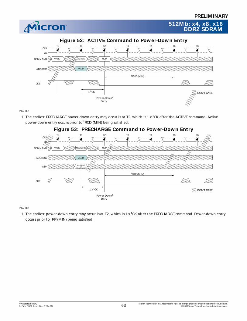
512Mb: x4, x8, x16DDR2 SDRAM
PRELIMINARY
Figure 52: ACTIVE Command to Power-Down Entry
NOTE:
1. The earliest PRECHARGE power-down entry may occur is at T2, which is 1 x tCK after the ACTIVE command. Active
power-down entry occurs prior to tRCD (MIN) being satisfied.
Figure 53: PRECHARGE Command to Power-Down Entry
NOTE:
1. The earliest power-down entry may occur is at T2, which is 1 x tCK after the PRECHARGE command. Power-down entry
occurs prior to tRP (MIN) being satisfied.
CK
CK#
COMMAND
DON’T CARE
T0 T1
VALID ACTIVE
T2
NOP
T3 T4 T5
tCKE (MIN)
CKE
T6
Power-Down1
Entry
1 tCK
ADDRESS VALID
CK
CK#
COMMAND
DON’T CARE
T0 T1
VALID PRECHARGE
T2
NOP
T3 T4 T5
tCKE (MIN)
CKE
T6
Power-Down1
Entry
1 x tCK
ADDRESS
A10
VALID
ALL BANKS vs
SINGLE BANK
09005aef80b88542 Micron Technology, Inc., reserves the right to change products or specifications without notice.512Mb_DDR2_2.fm - Rev. B 7/04 EN 63 ©2003 Micron Technology, Inc. All rights reserved.

512Mb: x4, x8, x16DDR2 SDRAM
PRELIMINARY
Figure 54: LOAD MODE Command to Power-Down Entry
NOTE:
1. The earliest PRECHARGE power-down entry is at T3, which is after tMRD is satisfied.
2. All banks must be in the precharged state and tRP met prior to issuing LM command.3. Valid address for LM command includes MR, EMR, EMR(2), and EMR(3) registers.
CK
CK#
COMMAND
DON’T CARE
T0 T1
VALID LM
T2
NOP
T3 T4 T5
tCKE (MIN)
CKE
T6
Power-Down1
Entry
tMRD
ADDRESS VALID3
tRP2
T7
NOP
09005aef80b88542 Micron Technology, Inc., reserves the right to change products or specifications without notice.512Mb_DDR2_2.fm - Rev. B 7/04 EN 64 ©2003 Micron Technology, Inc. All rights reserved.

512Mb: x4, x8, x16DDR2 SDRAM
PRELIMINARY
Precharge Power-Down Clock Frequency Change
When the DRAM is in precharged power-downmode, on-die termination (ODT) must be turned offand CKE must be at a logic LOW level. A minimum oftwo clocks must pass after CKE goes LOW before clockfrequency may change. The DRAM input clock fre-quency is allowed to change only within minimum andmaximum operating frequencies specified for the par-ticular speed grade. During input clock frequencychange, ODT and CKE must be held at stable LOW lev-
els. Once the input clock frequency is changed, newstable clocks must be provided to the DRAM beforeprecharge power-down may be exited and DLL mustbe RESET via EMR after precharge power-down exit.Depending on the new clock frequency an additionalMR command may need to be issued to appropriatelyset the WR MR[11, 10, 9] register. During the DLLrelock period of 200 cycles, ODT must remain off. Afterthe DLL lock time, the DRAM is ready to operate with anew clock frequency.
Figure 55: Input Clock Frequency Change During PRECHARGE Power Down Mode
NOTE:
1. If this command is a PRECHARGE (or if the device is already in the idle state), then the power-down mode shown is pre-charge power-down, which is required prior to the clock frequency change.
2. A minimum of 2 x tCK is required after entering PRECHARGE power-down prior to changing clock frequencies.
3. Once the new clock frequency has changed and is stable, a minimum of 1 x tCK is required prior to exiting PRECHARGE power-down.
4. Minimum CKE HIGH time is tCKE = 3 x tCK. Minimum CKE low time is tCKE = 3 x tCK. This requires a minimum of 3 clock cycles of registration.
CK
CK#
COMMAND VALID1 NOP
ADDR
CKE
DQ
DM
DQS, DQS#
NOP
tCK
Enter PRECHARGEPower-Down Mode
Exit PRECHARGEPower-Down Mode
T0 T1 T3 Ta0T2
DON’T CARE
VALID
tCKE (MIN)4
tCKE (MIN)4
tXP
LM
DLL RESET
VALID
VALID
NOP
tCH tCL
Ta1 Ta2 Tb0Ta3
2 x tCK (MIN)2 1 x tCK (MIN)3
tCH tCL
tCK
ODT
200 x tCK
NOP
Ta4
PREVIOUS CLOCK FREQUENCY NEW CLOCK FREQUENCY
FrequencyChange
High-Z
High-Z
Indicates a break in time scale
09005aef80b88542 Micron Technology, Inc., reserves the right to change products or specifications without notice.512Mb_DDR2_2.fm - Rev. B 7/04 EN 65 ©2003 Micron Technology, Inc. All rights reserved.

512Mb: x4, x8, x16DDR2 SDRAM
PRELIMINARY
RESET Function (CKE LOW Anytime)DDR2 SDRAM applications may go into a RESET
state at any time during normal operation. If an appli-cation enters a reset condition, the CKE input pin isused to ensure the DDR2 SDRAM device resumes nor-mal operation after reinitializing. All data will be lostduring a reset condition; however, the DDR2 SDRAMdevice will continue to operate properly if the follow-ing conditions outlined in this section are satisfied.
The RESET condition defined here assumes all sup-ply voltages (VDD, VDDQ, VDDL, and VREF ) are stableand meet all DC specifications prior to, during, andafter the RESET operation. All other input pins of the
DDR2 SDRAM device are a “don’t care” during RESETwith the exception of CKE.
If CKE asynchronously drops LOW during any validoperation (including a READ or WRITE burst), thememory controller must satisfy the timing parametertDELAY before turning off the clocks. Stable clocks mustexist at the CK, CK# inputs of DRAM before CKE israised HIGH, at which time the normal initializationsequence must occur (See “Initialization” on page 9).The DDR2 SDRAM is now ready for normal operationafter the initialization sequence. Figure 56 shows theproper sequence for a RESET condition.
Figure 56: RESET Condition
NOTE:
1. In certain cases where a READ cycle is interupted, CKE going high may result in the completion of the burst.
CKE
Rtt
BA0, BA1
High-Z
DM7
DQS7High-Z
ADDRESS
A10
CK
CK#
tCL
COMMAND6 NOP PRE
ALL BANKS
Ta0
DON’T CARE TRANSITIONING DATA
tRPA
tCL
tCK
ODT
DQ7 High-Z
T = 400ns (MIN)
Tb0
READ NOP
T0 T1 T2
Col n
Bank a
tDELAY
DOUTDOUT
()()
READ NOP
Col n
Bank b
DOUT
High-Z
High-Z
Unknown RTT ON
SystemRESET
T3 T4 T5
Start of NormalInitialization
Sequence
NOP
Indicates a break in time scale
tCKE(MIN)
1
For Initiliza-tion timing, see time sequence Ta0 in Figure 4, DDR2
Power-Up and Initialization, on page 10
09005aef80b88542 Micron Technology, Inc., reserves the right to change products or specifications without notice.512Mb_DDR2_2.fm - Rev. B 7/04 EN 66 ©2003 Micron Technology, Inc. All rights reserved.

512Mb: x4, x8, x16DDR2 SDRAM
PRELIMINARY
ODT TimingThere are two timing categories for ODT, turn-on
and turn-off. During active mode (CKE HIGH) and“fast-exit” power-down mode (any row of any bankopen, CKE LOW, MR[bit12 = 0]), tAOND, tAON, tAOFD,and tAOF timing parameters are applied as shown inFigure 57 and Table 10 on page 68. During “slow-exit”power-down mode (any row of any bank open, CKELOW, MR[bit12=1]) and precharge power-down mode(all banks/rows precharged and idle, CKE LOW),tAONPD and tAOFPD timing parameters are applied asshown in Figure 58 and Table 11 on page 69.
ODT turn-off timing prior to entering any power-down mode is determined by the parameter tANPD(MIN) shown in Figure 59. At state T2 the ODT HIGHsignal satisfies tANPD (MIN) prior to entering power-down mode at T5. When tANPD (MIN) is satisfiedtAOFD and tAOF timing parameters apply. Figure 59also shows the example where tANPD (MIN) is NOTsatisfied since ODT HIGH does not occur until stateT3. When tANPD (MIN) is NOT satisfied, tAOFPD tim-ing parameters apply.
ODT turn-on timing prior to entering any power-down mode is determined by the parameter tANPDshown in Figure 60. At state T2, the ODT HIGH signalsatisfies tANPD (MIN) prior to entering power-down
mode at T5. When tANPD (MIN) is satisfied tAONDand tAON timing parameters apply. Figure 60 alsoshows the example where tANPD (MIN) is NOT satis-fied since ODT HIGH does not occur until state T3.When tANPD (MIN) is NOT satisfied, tAONPD timingparameters apply.
ODT turn-off timing after exiting any power-downmode is determined by the parameter tAXPD (MIN)shown in Figure 61. At state Ta1, the ODT LOW signalsatisfies tAXPD (MIN) after exiting power-down modeat state T1. When tAXPD (MIN) is satisfied, tAOFD andtAOF timing parameters apply. Figure 61 also showsthe example where tAXPD (MIN) is NOT satisfied sinceODT LOW occurs at state Ta0. When tAXPD (MIN) isNOT satisfied, tAOFPD timing parameters apply.
ODT turn-on timing after exiting any power-downmode is determined by the parameter tAXPD (MIN)shown in Figure 62. At state Ta1, the ODT HIGH signalsatisfies tAXPD (MIN) after exiting power-down modeat state T1. When tAXPD (MIN) is satisfied, tAOND andtAON timing parameters apply. Figure 62 also showsthe example where tAXPD (MIN) is NOT satisfied sinceODT HIGH occurs at state Ta0. When tAXPD (MIN) isNOT satisfied, tAONPD timing parameters apply.
09005aef80b88542 Micron Technology, Inc., reserves the right to change products or specifications without notice.512Mb_DDR2_2.fm - Rev. B 7/04 EN 67 ©2003 Micron Technology, Inc. All rights reserved.

512Mb: x4, x8, x16DDR2 SDRAM
PRELIMINARY
Figure 57: ODT Timing for Active or “Fast-Exit” Power-Down Mode T1T0 T2 T3 T4 T5 T6
VALIDVALID VALID VALIDVALID VALID VALID
CK#
CK
CKE
tAOF (MAX)
ODT
RTTtAON (MIN)
tAON (MAX)
tAOND
ADDR
tAOFD
tAOF (MIN)
VALIDVALID VALID VALIDVALID VALID VALIDCMD
tCH tCLtCK
DON’T CARERTT Unknown RTT On
Table 10: ODT Timing for Active and “Fast-Exit” Power-Down Modes
PARAMETER SYMBOL MIN MAX UNITS
ODT turn-on delay tAOND 2 2 tCKODT turn-on tAON tAC (MIN) tAC (MAX) + 1,000 ps
ODT turn-off delay tAOFD 2.5 2.5 tCKODT turn-off tAOF tAC (MIN) tAC (MAX) + 600 ps
09005aef80b88542 Micron Technology, Inc., reserves the right to change products or specifications without notice.512Mb_DDR2_2.fm - Rev. B 7/04 EN 68 ©2003 Micron Technology, Inc. All rights reserved.

512Mb: x4, x8, x16DDR2 SDRAM
PRELIMINARY
Figure 58: ODT timing for “Slow-Exit” or Precharge Power-Down Modes
DON’T CARE
T1T0 T2 T3 T4 T5 T6
VALIDVALID VALID VALIDVALID VALID VALID
CK#
CK
CKE
ODT
RTT
ADDR
VALIDVALID VALID VALIDVALID VALID VALIDCMD
tCH tCLtCK
tAONPD (MIN)
tAONPD (MAX)
tAOFPD (MIN)tAOFPD (MAX)
Transitioning RTT
T7
VALID
VALID
RTT Unknown RTT On
Table 11: ODT timing for “Slow-Exit” and Precharge Power-Down Modes
PARAMETER SYMBOL MIN MAX UNITS
ODT turn-on (power-down mode) tAONPD tAC (MIN) + 2,000 2 x tCK+tAC (MAX) + 1,000 ps
ODT turn-off (power-down mode) tAOFPD tAC (MIN) + 2,000 2.5 x tCK + tAC (MAX) + 1,000 ps
09005aef80b88542 Micron Technology, Inc., reserves the right to change products or specifications without notice.512Mb_DDR2_2.fm - Rev. B 7/04 EN 69 ©2003 Micron Technology, Inc. All rights reserved.

512Mb: x4, x8, x16DDR2 SDRAM
PRELIMINARY
Figure 59: ODT “Turn Off” Timings when Entering Power-Down Mode T1T0 T2 T3 T4 T5 T6
NOPNOP NOP NOPNOP NOP NOP
CK#
CK
CKE
tANPD (MIN)
ODT
RTT
tAOF (MIN)
tAOF (MAX)
tAOFD
ODT
RTT
tAOFPD (MIN)
tAOFPD (MAX)
DON’T CARETransitioning RTT RTT Unknown RTT On
Table 12: ODT “Turn Off” Timings when Entering Power-Down Mode
PARAMETER SYMBOL MIN MAX UNITS
ODT turn-off delay tAOFD 2.5 2.5 tCKODT turn-off tAOF tAC (MIN) tAC (MAX) + 600 ps
ODT turn-off (power-down mode) tAOFPD tAC (MIN) + 2,000 2.5 x tCK + tAC (MAX) + 1,000 ps
ODT to power-down entry latency tANPD 3 tCK
09005aef80b88542 Micron Technology, Inc., reserves the right to change products or specifications without notice.512Mb_DDR2_2.fm - Rev. B 7/04 EN 70 ©2003 Micron Technology, Inc. All rights reserved.

512Mb: x4, x8, x16DDR2 SDRAM
PRELIMINARY
Figure 60: ODT “Turn-On” Timing when Entering Power-Down Mode T1T0 T2 T3 T4 T5 T6
NOPNOP NOP NOPNOP NOP NOP
CK#
CK
CKE
tANPD (MIN)
ODT
RTT
tAON (MIN)
tAON (MAX)
tAOND
ODT
RTT
tAONPD (MIN)
tAONPD (MAX)
DON’T CARETransitioning RTT RTT Unknown RTT On
Table 13: ODT “Turn-On” Timing when Entering Power-Down Mode
PARAMETER SYMBOL MIN MAX UNITS
ODT turn-on delay tAOND 2 2 tCKODT turn-on tAON tAC (MIN) tAC (MAX) + 1,000 ps
ODT turn-on (power-down mode) tAONPD tAC (MIN) + 2,000 2 x tCK + tAC (MAX) + 1,000 ps
ODT to power-down entry latency tANPD 3 tCK
09005aef80b88542 Micron Technology, Inc., reserves the right to change products or specifications without notice.512Mb_DDR2_2.fm - Rev. B 7/04 EN 71 ©2003 Micron Technology, Inc. All rights reserved.

512Mb: x4, x8, x16DDR2 SDRAM
PRELIMINARY
Figure 61: ODT “Turn-Off” Timing when Exiting Power-Down Mode T1T0 T2 T3 T4 Ta0 Ta1
NOPNOP NOP NOPNOP NOP NOP
CK#
CK
CKE
tAXPD (MIN)
ODT
RTT
tAOF (MAX)
ODT
RTT
tAOFPD (MIN)
tAOFPD (MAX)
COMMAND
tCKE (MIN)
Ta2 Ta3 Ta4 Ta5
NOPNOP NOP NOP
DON’T CARETransitioning RTT RTT Unknown RTT On
tAOF (MIN)
tAOFD
Indicates a break in time scale
Table 14: ODT “Turn-Of” Timing when Exiting Power-Down Mode
PARAMETERSYMBOL
MIN MAX UNITS
ODT turn-off delay tAOFD 2.5 2.5 tCKODT turn-off tAOF tAC (MIN) tAC (MAX) + 600 ps
ODT turn-off (power-down mode) tAOFPD tAC (MIN) + 2,000 2.5 x tCK + tAC (MAX) + 1,000 ps
ODT to power-down exit latency tAXPD 8 tCK
09005aef80b88542 Micron Technology, Inc., reserves the right to change products or specifications without notice.512Mb_DDR2_2.fm - Rev. B 7/04 EN 72 ©2003 Micron Technology, Inc. All rights reserved.

512Mb: x4, x8, x16DDR2 SDRAM
PRELIMINARY
Figure 62: ODT “Turn On” Timing when Exiting Power-Down Mode T1T0 T2 T3 T4 Ta0 Ta1
NOPNOP NOP NOPNOP NOP NOP
CK#
CK
CKE
tAXPD (MIN)
COMMAND
Ta2 Ta3 Ta4 Ta5
NOPNOP NOP NOP
ODT
RTT
tAON (MIN)
tAON (MAX)
tAOND
ODT
RTT
tAONPD (MIN)
tAONPD (MAX)
DON’T CARETransitioning RTT RTT Unknown RTT OnIndicates a break in time scale
tCKE (MIN)
Table 15: ODT “Turn On” Timing when Exiting Power-Down Mode
PARAMETERSYMBOL
MIN MAX UNITS
ODT turn-on delay tAOND 2 2 tCKODT turn-on tAON tAC (MIN) tAC (MAX) + 1,000 ps
ODT turn-on (power-down mode) tAONPD tAC (MIN) + 2,000 2 x tCK + tAC (MAX) + 1,000 ps
ODT to power-down exit latency tAXPD 8 tCK
09005aef80b88542 Micron Technology, Inc., reserves the right to change products or specifications without notice.512Mb_DDR2_2.fm - Rev. B 7/04 EN 73 ©2003 Micron Technology, Inc. All rights reserved.

512Mb: x4, x8, x16DDR2 SDRAM
PRELIMINARY
Absolute Maximum RatingsStresses greater than those listed may cause perma-
nent damage to the device. This is a stress rating only,and functional operation of the device at these or anyother conditions above those indicated in the opera-
tional sections of this specification is not implied.Exposure to absolute maximum rating conditions forextended periods may affect reliability.
Figure 63: Example Temperature Test Point Location
Table 16: Absolute Maximum DC Ratings
SYMBOL PARAMETER MIN MAX UNITS
VDD VDD Supply Voltage Relative to VSS -1.0 2.3 V
VDDQ VDDQ Supply Voltage Relative to VSSQ -0.5 2.3 V
VDDL VDDL Supply Voltage Relative to VssL -0.5 2.3 V
VIN, VOUT Voltage on any Pin Relative to VSS -0.5 2.3 VTSTG Storage Temperature (Tcase)1 -55 100 °C
TC Operating Temperature (Tcase)1,2 0 85 °C
II Input Leakage CurrentAny input 0V <= VIN <= VDD(All other pins not under test = 0V)
-5 5 uA
IOZ Output Leakage Current0V <= VOUT <= VDDQDQs and ODT are disabled
-5 5 uA
IVREF VREF Leakage CurrentVREF = Valid VREF level
-2 2 uA
NOTE:
1. MAX operating case temperature; TC is measured in the center of the package illustrated in Figure 63.2. Device functionality is not guaranteed if the DRAM device exceeds the maximum TC during operation.
11.00
5.50
19.00
9.50
11m x 19mm “BT” FBGA
Test Point
09005aef80b88542 Micron Technology, Inc., reserves the right to change products or specifications without notice.512Mb_DDR2_2.fm - Rev. B 7/04 EN 74 ©2003 Micron Technology, Inc. All rights reserved.

512Mb: x4, x8, x16DDR2 SDRAM
PRELIMINARY
AC and DC Operating Conditions
NOTE:
1. VDD and VDDQ must track each other. VDDQ must be less than or equal to VDD.2. VREF is expected to equal VDDQ/2 of the transmitting device and to track variations in the DC level of the same. Peak-to-
peak noise (non-common mode) on VREF may not exceed ±1% of the DC value. Peak-to-peak AC noise on VREF may not exceed ±2 percent of VREF(DC). This measurement is to be taken at the nearest VREF bypass capacitor.
3. VTT is not applied directly to the device. VTT is a system supply for signal termination resistors, is expected to be set equal to VREF and must track variations in the DC level of VREF.
4. VDDQ tracks with VDD; VDDL tracks with VDD.5. VssQ = VssL = Vss
NOTE:
1. RTT1(EFF) and RTT2(EFF) are determined by applying VIH(AC) and VIL(AC) to pin under test separately, then measure current I(VIH(AC)) and I(VIL(AC)) respectively.
2. Measure voltage (VM) at tested pin with no load.
Table 17: Recommended DC Operating Conditions (SSTL_18)All voltages referenced to VSS
PARAMETER SYMBOL MIN NOM MAX UNITS NOTES
Supply Voltage VDD 1.7 1.8 1.9 V 1, 5
VDDL Supply Voltage VDDL 1.7 1.8 1.9 V 4, 5
I/O Supply Voltage VDDQ 1.7 1.8 1.9 V 4, 5
I/O Reference Voltage VREF(DC) 0.49 x VDDQ 0.50 x VDDQ 0.51 X VDDQ V 2
I/O Termination Voltage (system) VTT VREF(DC) - 40 VREF(DC) VREF(DC) + 40 mV 3
Table 18: ODT DC Electrical CharacteristicsAll voltages referenced to VSS
PARAMETER SYMBOL MIN NOM MAX UNITS NOTES
RTT effective impedance value for 75Ω settingEMR (A6, A2) = 0, 1
RTT1(EFF) 60 75 90 Ω 1
RTT effective impedance value for 150Ω settingEMR (A6, A2) = 1, 0
RTT2(EFF) 120 150 180 Ω 1
Deviation of VM with respect to VDDQ/2 ∆VM -6% 6% % 2
RTT EFF( ) VIH AC( ) VIL AC( )–I VIH AC( )( ) I VIL AC( )( )–-------------------------------------------------------------=
∆VM 2 VM×VDDQ------------------ 1–
100%×=
09005aef80b88542 Micron Technology, Inc., reserves the right to change products or specifications without notice.512Mb_DDR2_2.fm - Rev. B 7/04 EN 75 ©2003 Micron Technology, Inc. All rights reserved.

512Mb: x4, x8, x16DDR2 SDRAM
PRELIMINARY
Input Electrical Characteristics and Operating Conditions
Figure 64: Single-Ended Input Signal Levels
NOTE:
Numbers in diagram reflect nomimal values.
Table 19: Input DC Logic LevelsAll voltages referenced to VSS
PARAMETER SYMBOL MIN MAX UNITS NOTES
Input High (Logic 1) Voltage VIH(DC) VREF(DC) + 125 VDDQ + 300 mV
Input Low (Logic 0) Voltage VIL(DC) -300 VREF(DC) - 125 mV
Table 20: Input AC Logic LevelsAll voltages referenced to VSS
PARAMETER SYMBOL MIN MAX UNITS NOTES
Input High (Logic 1) Voltage VIH(AC) VREF(DC) + 250 - mV
Input Low (Logic 0) Voltage VIL(AC) – VREF(DC) - 250 mV
650mV
775mV
864mV882mV900mV918mV936mV
1,025mV
1,150mV
VIL (AC)
VIL (DC)
VREF - AC NoiseVREF - DC ErrorVREF + DC ErrorVREF + AC Noise
VIH (DC)
VIH (AC)
09005aef80b88542 Micron Technology, Inc., reserves the right to change products or specifications without notice.512Mb_DDR2_2.fm - Rev. B 7/04 EN 76 ©2003 Micron Technology, Inc. All rights reserved.

512Mb: x4, x8, x16DDR2 SDRAM
PRELIMINARY
NOTE:
1. VIN (DC) specifies the allowable DC execution of each input of differential pair such as CK, CK#, DQS, DQS#, LDQS, LDQS#, UDQS, UDQS#, and RDQS, RDQS#.
2. VID (DC) specifies the input differential voltage | VTR - VCP | required for switching, where VTR is the true input (such as CK, DQS, LDQS, UDQS, RDQS) level and VCP is the complementary input (such as CK#, DQS#, LDQS#, UDQS#, RDQS#). The minimum value is equal to VIH(DC) - VIL(DC). Differential input signal levels are shown in Figure 65.
3. VID(AC) specifies the input differential voltage | VTR - VCP | required for switching, where VTR is the true input (such as CK, DQS, LDQS, UDQS, RDQS) level and VCP is the complementary input (such as CK#, DQS#, LDQS#, UDQS#, RDQS#). The minimum value is equal to VIH(AC) - VIL(AC) from Table 20 on page 76.
4. The typical value of VIX (AC) is expected to be about 0.5 x VDDQ of the transmitting device and VIX(AC) is expected to track variations in VDDQ. VIX(AC) indicates the voltage at which differential input signals must cross as shown in Figure 65.
5. VMP(DC) specifies the input differential common mode voltage (VTR + VCP)/2 where VTR is the true input (CK, DQS) level and VCP is the complementary input (CK#, DQS#). VMP(DC) is expected to be about 0.5*VDDQ.
Figure 65: Differential Input Signal Levels
NOTE:
1. This provides a minimum of 850mV to a maximum of 950mV and is expected to be VDDQ/2.2. TR and CP must cross in this region.3. TR and CP must meet at least VID(DC) min when static and is centered around VMP(DC).4. TR and CP must have a minimum 500mV peak-to-peak swing.5. TR and CP may not be more positive than VDDQ + 0.3V or more negative than VSS - 0.3V.6. For AC operation, all DC clock requirements must also be satisfied.7. Numbers in diagram reflect nominal values.8. TR represents the CK, DQS, RDQS, LDQS and UDQS signals; CP represents CK#, DQS#, RDQS#, LDQS# and UDQS# signals.
Table 21: Differential Input Logic LevelsAll voltages referenced to VSS
PARAMETER SYMBOL MIN MAX UNITS NOTES
DC Input Signal Voltage VIN(DC) -300 VDDQ + 300 mV 1
DC Differential Input Voltage VID(DC) 250 VDDQ + 600 mV 2
AC Differential Input Voltage VID(AC) 500 VDDQ + 600 mV 3
AC Differential Cross-Point Voltage VIX(AC) 0.50 x VDDQ - 175 0.50 x VDDQ + 175 mV 4
Input Midpoint Voltage VMP(DC) 850 950 mV 5
CP8
TR8
2.1 V@ VDDQ=1.8V
23
VIN(DC) MAX5
VIN(DC) MIN5
4
- 0.30V
0.9V
1.075 V
0.725 VVID (AC)
VID (DC)
X
1VMP (DC)
VIX (AC)
X
09005aef80b88542 Micron Technology, Inc., reserves the right to change products or specifications without notice.512Mb_DDR2_2.fm - Rev. B 7/04 EN 77 ©2003 Micron Technology, Inc. All rights reserved.

512Mb: x4, x8, x16DDR2 SDRAM
PRELIMINARY
NOTE:
1. All voltages referenced to VSS.
2. Input waveform setup timing (tISb) is referenced from the input signal crossing at the VIH(AC) level for a rising signal and VIL(DC) for a falling signal applied to the device under test as shown in Figure 74.
3. Input waveform hold (tIHb) timing is referenced from the input signal crossing at the VIL(DC) level for a rising signal and VIH(DC) for a falling signal applied to the device under test as shown in Figure 74
4. Input waveform setup timing (tDS) and hold timing (tDH) for single-ended data strobe is referenced from the crossing of DQS, UDQS, or LDQS through the VREF level applied to the device under test as shown in Figure 76.
5. Input waveform setup timing (tDS) and hold timing (tDH) when differential data strobe is enabled is referenced from the crosspoint of DQS,DQS# or UDQS,UDQS# or LDQS,LDQS# as shown in Figure 75.
6. Input waveform timing is referenced to the crossing point level (VIX) of two input signals (VTR and VCP) applied to the device under test, where VTR is the “true” input signal and VCP is the “complementary” input signal shown in Figure 77.
7. See “Input Slew Rate Derating” on page 79.
Table 22: AC Input Test Conditions
PARAMETER SYMBOL MIN MAX UNITS NOTES
Input setup timing measurement reference level BA1-BA0, A0-A13 (A12 x16), CS#, RAS#, CAS#, WE#, ODT, DM, UDM, LDM and CKE
VRS See Note 2 1, 2,
Input hold timing measurement reference level BA1-BA0, A0-A13 (A12 x16), CS#, RAS#, CAS#, WE#, ODT, DM, UDM, LDM and CKE
VRH See Note3 1, 3,
Input timing measurement reference level (single-ended) DQS for x4x8; UDQS, LDQS for x16
VREF(DC) VDDQ*0.49 VDDQ*0.51 V 1, 4
Input timing measurement reference level (differential)CK, CK# for x4,x8,x16DQS, DQS# for x4,x8; RDQS, RDQS# for x8UDQS, UDQS#, LDQS, LDQS# for x16
VRD VIX(AC) V 1, 5, 6
09005aef80b88542 Micron Technology, Inc., reserves the right to change products or specifications without notice.512Mb_DDR2_2.fm - Rev. B 7/04 EN 78 ©2003 Micron Technology, Inc. All rights reserved.

512Mb: x4, x8, x16DDR2 SDRAM
PRELIMINARY
Input Slew Rate DeratingFor all input signals the total tIS (setup time) and tIH
(hold time) required is calculated by adding the datasheet tIS(base) and tIH(base) value to the ∆tIS and ∆tIHderating value respectively. Example: tIS (total setuptime) = tIS(base) + ∆tIS
Setup (tIS) nominal slew rate for a rising signal isdefined as the slew rate between the last crossing ofVREF(DC) and the first crossing of VIH(AC)min. Setup(tIS) nominal slew rate for a falling signal is defined asthe slew rate between the last crossing of VREF(DC) andthe first crossing of VIL(AC)MAX. If the actual signal isalways earlier than the nominal slew rate line betweenshaded ‘VREF(DC) to AC region’, use nominal slew ratefor derating value (Figure 66 on page 80) If the actualsignal is later than the nominal slew rate line anywherebetween shaded ‘VREF(DC) to ac region’, the slew rate ofa tangent line to the actual signal from the AC level toDC level is used for derating value (Figure 67 onpage 80)
Hold (tIH) nominal slew rate for a rising signal isdefined as the slew rate between the last crossing ofVIL(DC)MAX and the first crossing of VREF(DC). Hold
(tIH) nominal slew rate for a falling signal is defined asthe slew rate between the last crossing of VIH(DC)MIN
and the first crossing of VREF(DC). If the actual signal isalways later than the nominal slew rate line betweenshaded ‘dc to VREF(DC) region’, use nominal slew ratefor derating value (Figure 68 on page 81) If the actualsignal is earlier than the nominal slew rate line any-where between shaded ‘dc to VREF(DC) region’, the slewrate of a tangent line to the actual signal from the dclevel to VREF(DC) level is used for derating value(Figure 69 on page 81)
Although for slow slew rates the total setup timemight be negative (i.e. a valid input signal will not havereached VIH/IL(AC) at the time of the rising clock tran-sition) a valid input signal is still required to completethe transition and reach VIH/IL(AC)).
For slew rates in between the values listed inTable 23, the derating values may obtained by linearinterpolation.
Table 23: Setup and Hold Time Derating Values
CK,CK# DIFFERENTIAL SLEW RATE
2.0 V/NS 1.5 V/NS 1.0 V/NS
∆tIS ∆tIH ∆tIS ∆tIH ∆tIS ∆tIH UNITS
Command/Address Slew
rate(V/ns)
4.0 +187 +94 +217 +124 +247 +154 ps3.5 +179 +89 +209 +119 +239 +149 ps3.0 +167 +83 +197 +113 +227 +143 ps2.5 +150 +75 +180 +105 +210 +135 ps2.0 +125 +45 +155 +75 +185 +105 ps1.5 +83 +21 +113 +51 +143 +81 ps1.0 0 0 +30 +30 +60 +60 ps0.9 -11 -14 +19 +16 +49 +46 ps0.8 -25 -31 +5 -1 +35 +29 ps0.7 -43 -54 -13 -24 +17 +6 ps0.6 -67 -83 -37 -53 -7 -23 ps0.5 -110 -125 -80 -95 -50 -65 ps0.4 -175 -188 -145 -158 -115 -128 ps0.3 -285 -292 -255 -262 -225 -232 ps
0.25 -350 -375 -320 -345 -290 -315 ps0.2 -525 -500 -495 -470 -465 -440 ps
0.15 -800 -708 -770 -678 -740 -648 ps0.1 -1450 -1125 -1420 -1095 -1390 -1065 ps
09005aef80b88542 Micron Technology, Inc., reserves the right to change products or specifications without notice.512Mb_DDR2_2.fm - Rev. B 7/04 EN 79 ©2003 Micron Technology, Inc. All rights reserved.

512Mb: x4, x8, x16DDR2 SDRAM
PRELIMINARY
Figure 66: Nominal Slew Rate for tIS
Figure 67: Tangent Line for tIS
VSS
CK
CK
tIHtIS tIH
Setup Slew RateSetup Slew RateRising SignalFalling Signal
Delta TF Delta TR
VREF(dc) - Vil(ac)max
Delta TF=
Vih(ac)min - VREF(dc)Delta TR
=
VDDQ
VIH(ac) min
VIH(dc) min
VREF(dc)
VIL(dc) max
VIL(ac) max
tIS
nominal slewrate
nominalslew rate
VREF to ac region
VREF to ac region
VSS
CK
CK
tIHtIS tIH
Setup Slew Rate
Rising SignalDelta TF
Delta TR
tangent line[Vih(ac)min - VREF(dc)]
Delta TR=
VDDQ
VIH(ac) min
VIH(dc) min
VREF(dc)
VIL(dc) max
VIL(ac) max
tIS
tangent
tangent
VREF to ac region
VREF to ac region
line
line
nominal line
nominal line
09005aef80b88542 Micron Technology, Inc., reserves the right to change products or specifications without notice.512Mb_DDR2_2.fm - Rev. B 7/04 EN 80 ©2003 Micron Technology, Inc. All rights reserved.

512Mb: x4, x8, x16DDR2 SDRAM
PRELIMINARY
Figure 68: Nominal Slew Rate for tIH
Figure 69: Tangent Line for tIH
VSS
CK
CK
tIHtIS tIH
Delta TR Delta TF
VDDQ
VIH(ac) min
VIH(dc) min
VREF(dc)
VIL(dc) max
VIL(ac) max
tIS
nominalslew rate
nominalslew rate
dc to VREF region
dc to VREF region
VSS
CK
CK
tIHtIS tIH
Hold Slew Rate
Delta TFDelta TR
tangent line [ Vih(dc)min - VREF(dc) ]
Delta TF=
VDDQ
VIH(ac) min
VIH(dc) min
VREF(dc)
VIL(dc) max
VIL(ac) max
tIS
tangent
tangentdc to VREF region
dc to VREF region
line
linenominal line
nominal line
Falling Signal
Hold Slew Rate tangent line [ VREF(dc) - Vil(dc)max ]
Delta TR= Rising Signal
09005aef80b88542 Micron Technology, Inc., reserves the right to change products or specifications without notice.512Mb_DDR2_2.fm - Rev. B 7/04 EN 81 ©2003 Micron Technology, Inc. All rights reserved.

512Mb: x4, x8, x16DDR2 SDRAM
PRELIMINARY
Data Slew Rating
NOTE:
1. For all input signals the total tDS (setup time) and tDH (hold time) required is calculated by adding the datasheet value to the derating value listed in Table 24.
2. Setup (tDS) nominal slew rate for a rising signal is defined as the slew rate between the last crossing of VREF(dc) and the
first crossing of Vih(ac)min. Setup (tDS) nominal slew rate for a falling signal is defined as the slew rate between the last crossing of VREF(dc) and the first crossing of Vil(ac)max. If the actual signal is always earlier than the nominal slew rate line between shaded ‘VREF(dc) to ac region’, use nominal slew rate for derating value (see Figure 70) If the actual signal is later than the nominal slew rate line anywhere between shaded ‘VREF(dc) to ac region’, the slew rate of a tangent line to the actual signal from the ac level to dc level is used for derating value (see Figure 71)
3. Hold (tDH) nominal slew rate for a rising signal is defined as the slew rate between the last crossing of Vil(dc)max and
the first crossing of VREF(dc). Hold (tDH) nominal slew rate for a falling signal is defined as the slew rate between the last crossing of Vih(dc)min and the first crossing of VREF(dc). If the actual signal is always later than the nominal slew rate line between shaded ‘dc level to VREF(dc) region’, use nominal slew rate for derating value (see Figure 72) If the actual signal is earlier than the nominal slew rate line anywhere between shaded ‘dc to VREF(dc) region’, the slew rate of a tangent line to the actual signal from the dc level to VREF(dc) level is used for derating value (see Figure 73)
4. Although for slow slew rates the total setup time might be negative (i.e. a valid input signal will not have reached VIH/
IL(ac) at the time of the rising clock transition) a valid input signal is still required to complete the transition and reach VIH/IL(ac).
5. For slew rates in between the values listed in Table 24, the derating values may obtained by linear interpolation.6. These values are typically not subject to production test. They are verified by design and characterization.
Table 24: tDS, tDH Derating Values Note 1; all units in ps
DQS,DQS# DIFFERENTIAL SLEW RATE
4.0 V/ns 3.0 V/ns 2.0 V/ns 1.8 V/ns 1.6 V/ns 1.4V/ns 1.2V/ns 1.0V/ns 0.8V/ns
∆tDS ∆tDH ∆tDS ∆tDH ∆tDS ∆tDH ∆tDS ∆tDH ∆tDS ∆tDH ∆tDS ∆tDH ∆tDS ∆tDH ∆tDS ∆tDH ∆tDS ∆tDH
DQ
Sle
w r
ate
V/n
s
2.0 125 45 125 45 125 45 - - - - - - - - - - - -
1.5 83 21 83 21 83 21 95 33 - - - - - - - - - -
1.0 0 0 0 0 0 0 12 12 24 24 - - - - - - - -
0.9 - - -11 -14 -11 -14 1 -2 13 10 25 22 - - - - - -
0.8 - - - - -25 -31 -13 -19 -1 -7 11 5 23 17 - - - -
0.7 - - - - - - -31 -42 -19 -30 -7 -18 5 -6 17 6 - -
0.6 - - - - - - - - -43 -59 -31 -47 -19 -35 -7 -23 5 -11
0.5 - - - - - - - - - - -74 -89 -62 -77 -50 -65 -38 -53
0.4 - - - - - - - - - - - - -127 -140 -115 -128 -103 -116
09005aef80b88542 Micron Technology, Inc., reserves the right to change products or specifications without notice.512Mb_DDR2_2.fm - Rev. B 7/04 EN 82 ©2003 Micron Technology, Inc. All rights reserved.

512Mb: x4, x8, x16DDR2 SDRAM
PRELIMINARY
Figure 70: Nominal Slew Rate for tDS
Figure 71: Tangent Line for tDS
VSS
DQSNOTE1
DQSNOTE1
tDHtDS tDH
Setup Slew RateSetup Slew RateRising SignalFalling Signal
Delta TF Delta TR
V REF(dc) - Vil(ac)max
Delta TF=
Vih(ac)min - V REF(dc)Delta TR
=
VDDQ
VIH(ac) min
VIH(dc) min
VREF(dc)
VIL(dc) max
VIL(ac) max
tDS
nominal slewrate
nominalslew rate
VREF to ac region
VREF to ac region
NOTE1 DQS, DQS# signals must be monotonic between Vil(dc)max and Vih(dc)min.
VSS
DQSNOTE1
DQSNOTE1
tDHtDS tDH
Setup Slew Rate
Setup Slew Rate
Rising Signal
Falling Signal
Delta TF
Delta TR
tangent line[V REF(dc) - Vil(ac)max]
Delta TF=
tangent line[Vih(ac)min - V REF(dc) ]
Delta TR=
VDDQ
V IH(ac) min
V IH(dc) min
V REF(dc)
V IL(dc) max
V IL(ac) max
tDS
tangent
tangent
VREF to ac region
VREF to ac region
line
line
nominal line
nominal line
NOTE1 DQS, DQS# signals must be monotonic between Vil(dc)max and Vih(dc)min.
09005aef80b88542 Micron Technology, Inc., reserves the right to change products or specifications without notice.512Mb_DDR2_2.fm - Rev. B 7/04 EN 83 ©2003 Micron Technology, Inc. All rights reserved.

512Mb: x4, x8, x16DDR2 SDRAM
PRELIMINARY
Figure 72: Nominal Slew Rate for tDH
Figure 73: Tangent Line for tDH
VSS
DQSNOTE1
DQSNOTE1
tDHtDS tDH
Hold Slew RateHold Slew Rate
Falling SignalRising Signal
Delta TR Delta TF
V REF(dc) - Vil(dc)max
Delta TR= Vih(dc)min - V REF(dc)
Delta TF=
VDDQ
VIH(ac) min
VIH(dc) min
V REF(dc)
VIL(dc) max
VIL(ac) max
tDS
nominalslew rate
nominalslew rate
dc to VREF region
dc to VREF region
NOTE1 DQS, DQS# signals must be monotonic between Vil(dc)max and Vih(dc)min.
VSS
DQSNOTE1
DQSNOTE1
tDHtDS tDH
Hold Slew Rate
Delta TFDelta TR
tangent line [ Vih(dc)min - V REF(dc) ]
Delta TF=
VDDQ
V IH(ac) min
V IH(dc) min
V REF(dc)
V IL(dc) max
V IL(ac) max
tDS
tangent
tangentdc to VREF region
dc to VREF region
line
linenominal line
nominal line
Falling Signal
Hold Slew Rate tangent line [ V REF(dc) - Vil(dc)max ]
Delta TR= Rising Signal
NOTE1 DQS, DQS# signals must be monotonic between Vil(dc)max and Vih(dc)min.
09005aef80b88542 Micron Technology, Inc., reserves the right to change products or specifications without notice.512Mb_DDR2_2.fm - Rev. B 7/04 EN 84 ©2003 Micron Technology, Inc. All rights reserved.

512Mb: x4, x8, x16DDR2 SDRAM
PRELIMINARY
Figure 74: AC Input Test Signal Waveform Command/Address pins
Figure 75: AC Input Test Signal Waveform for Data with DQS,DQS# (differential)
VREF(DC)
VIL(DC) MAX
VIL(AC) MAX
VSSQ
VIH(DC) MIN
VIH(AC) MIN
VDDQ
V SW
ING
(M
AX
)
tISa
Logic Levels
VREF Levels tIHatISa
tIHa
tISbtIHb
tISbtIHb
CK#
CK
VREF(DC)
VIL(DC) MAX
VIL(AC) MAX
VSSQ
VIH(DC) MIN
VIH(AC) MIN
VDDQ
V SW
ING
(M
AX
)
DQS#
DQS
tDSatDHa
tDSatDHa
tDSbtDHb
tDSbtDHb
Logic Levels
VREF Levels
09005aef80b88542 Micron Technology, Inc., reserves the right to change products or specifications without notice.512Mb_DDR2_2.fm - Rev. B 7/04 EN 85 ©2003 Micron Technology, Inc. All rights reserved.

512Mb: x4, x8, x16DDR2 SDRAM
PRELIMINARY
Figure 76: AC Input Test Signal Waveform for Data with DQS (single-ended)
Figure 77: AC Input Test Signal Waveform (differential)
VREF(DC)
VIL(DC) MAX
VIL(AC) MAX
VSSQ
VIH(DC) MIN
VIH(AC) MIN
VDDQ
V SW
ING
(M
AX
)DQS
VREF
Logic Levels
VREF LevelsVREF LevelstDSa
tDHatDSa
tDHa
tDSbtDHb
tDSbtDHb
VTR
VSWING
VCP
VDDQ
VSSQ
VIX
Crossing Point
09005aef80b88542 Micron Technology, Inc., reserves the right to change products or specifications without notice.512Mb_DDR2_2.fm - Rev. B 7/04 EN 86 ©2003 Micron Technology, Inc. All rights reserved.

512Mb: x4, x8, x16DDR2 SDRAM
PRELIMINARY
Power and Ground Clamp CharacteristicsPower and ground clamps are provided on the fol-
lowing input-only pins: BA1-BA0, A0-A13 (A12 x16),CS#, RAS#, CAS#, WE#, ODT, and CKE.
Figure 78: Input Clamp Characteristics
Table 25: Input Clamp Characteristics
VOLTAGE ACROSS CLAMP(V)
MINIMUM POWER CLAMP CURRENT (mA)
MINIMUM GROUND CLAMP CURRENT (mA)
0.0 0.0 0.00.1 0.0 0.00.2 0.0 0.00.3 0.0 0.00.4 0.0 0.00.5 0.0 0.00.6 0.0 0.00.7 0.0 0.00.8 0.1 0.10.9 1.0 1.01.0 2.5 2.51.1 4.7 4.71.2 6.8 6.81.3 9.1 9.11.4 11.0 11.01.5 13.5 13.51.6 16.0 16.01.7 18.2 18.21.8 21.0 21.0
0.0
5.0
10.0
15.0
20.0
25.0
0.0 0.1 0.2 0.3 0.4 0.5 0.6 0.7 0.8 0.9 1.0 1.1 1.2 1.3 1.4 1.5 1.6 1.7 1.8
Voltage Across Clamp (V)
Min
imu
m C
lam
p C
urr
ent
(mA
)
09005aef80b88542 Micron Technology, Inc., reserves the right to change products or specifications without notice.512Mb_DDR2_2.fm - Rev. B 7/04 EN 87 ©2003 Micron Technology, Inc. All rights reserved.

512Mb: x4, x8, x16DDR2 SDRAM
PRELIMINARY
AC Overshoot/Undershoot Specification
Figure 79: Overshoot
Figure 80: Undershoot
Table 26: Address and Control PinsApplies to BA1-BA0, A0-A13 (A12 x16), CS#, RAS#, CAS#, WE#, CKE, ODT
PARAMETER
SPECIFICATION
-5E -37E
Maximum peak amplitude allowed for overshoot area (See Figure 79) 0.9V 0.9V
Maximum peak amplitude allowed for undershoot area (See Figure 80) 0.9V 0.9V
Maximum overshoot area above VDD (See Figure 79) 0.75V-ns 0.56V-ns
Maximum undershoot area below VSS (See Figure 80) 0.75V-ns 0.56V-ns
Table 27: Clock, Data, Strobe, and Mask PinsApplies to DQ0–DQxx, DQS, DQS#, RDQS, RDQS#, UDQS, UDQS#, LDQS, LDQS#, DM, UDM, LDM
PARAMETER
SPECIFICATION
-5E -37E
Maximum peak amplitude allowed for overshoot area (See Figure 79) 0.9V 0.9V
Maximum peak amplitude allowed for undershoot area (See Figure 79) 0.9V 0.9V
Maximum overshoot area above VDDQ (See Figure 79) 0.38V-ns 0.28V-ns
Maximum undershoot area below VSSQ (See Figure 80) 0.38V-ns 0.28V-ns
Overshoot AreaMaximum Amplitude
VDD/VDDQ
VSS/VSSQ
Volts
Time (ns)
(V)
Undershoot AreaMaximum Amplitude
VSS/VSSQVolts
Time (ns)
(V)
09005aef80b88542 Micron Technology, Inc., reserves the right to change products or specifications without notice.512Mb_DDR2_2.fm - Rev. B 7/04 EN 88 ©2003 Micron Technology, Inc. All rights reserved.

512Mb: x4, x8, x16DDR2 SDRAM
PRELIMINARY
Output Electrical Characteristics and Operating Conditions
NOTE:
1. The typical value of VOX(AC) is expected to be about 0.5 x VDDQ of the transmitting device and VOX (AC) is expected to track variations in VDDQ. VOX(AC) indicates the voltage at which differential output signals must cross.
Figure 81: Differential Output Signal Levels
Table 28: Differential AC Output Parameters
PARAMETER SYMBOL MIN MAX UNITS NOTES
AC Differential Cross-Point Voltage VOX(AC) 0.50 x VDDQ - 125 0.50 x VDDQ + 125 mV 1
AC Differential Voltage Swing VSWING 1.0 mV
VTR
VSWING
VCP
VDDQ
VSSQ
VOX
Crossing Point
09005aef80b88542 Micron Technology, Inc., reserves the right to change products or specifications without notice.512Mb_DDR2_2.fm - Rev. B 7/04 EN 89 ©2003 Micron Technology, Inc. All rights reserved.

512Mb: x4, x8, x16DDR2 SDRAM
PRELIMINARY
NOTE:
1. For IOH (DC); VDDQ = 1.7V, VOUT = 1420mV. (VOUT - VDDQ)/IOH must be less than 21Ω for values of VOUT between VDDQ and VDDQ - 280mV.
2. For IOL (DC); VDDQ = 1.7V, VOUT = 280mV. VOUT/IOL must be less than 21Ω for values of VOUT between 0V and 280mV.3. The DC value of VREF applied to the receiving device is set to VTT.4. The values of IOH (DC) and IOL (DC) are based on the conditions given in Notes 1 and 2. They are used to test device drive
current capability to ensure VIH (MIN) plus a noise margin and VIL (MAX) minus a noise margin are delivered to an SSTL_18 receiver. The actual current values are derived by shifting the desired driver operating point (See output IV curves) along a 21Ω load line to define a convenient driver current for measurement.
NOTE:
1. Absolute specifications: 0°C ≤ Tcase ≤ +85°C; VDDQ = +1.8V ±0.1V, VDD = +1.8V ±0.1V.2. Impedance measurement condition for output source DC current: VDDQ = 1.7V; VOUT = 1420mV; (VOUT - VDDQ)/IOH must
be less than 23.4Ω for values of VOUT between VDDQ and VDDQ - 280mV. Impedance measurement condition for output sink DC current: VDDQ = 1.7V; VOUT = 280mV; VOUT/IOL must be less than 23.4Ω for values of VOUT between 0V and 280mV.
3. Mismatch is absolute value between pull-up and pull-down, both are measured at same temperature and voltage.4. Output slew rate for falling and rising edges is measured between VTT - 250mV and VTT + 250mV for single ended sig-
nals. For differential signals (e.g. DQS - DQS#) output slew rate is measured between DQS - DQS# = -500mV and DQS# - DQS = +500mV. Output slew rate is guaranteed by design, but is not necessarily tested on each device.
5. The absolute value of the slew rate as measured from VIL (DC)MAX to VIH (DC) MIN is equal to or greater than the slew rate as measured from VIL (AC) MAX to VIH (AC) MIN. This is guaranteed by design and characterization.
Figure 82: Output Slew Rate Load
Table 29: Output DC Current Drive
PARAMETER SYMBOL VALUE UNITS NOTES
Output Minimum Source DC Current IOH -13.4 mA 1,3,4
Output Minimum Sink DC Current IOL 13.4 mA 2,3,4
Table 30: Output Characteristics
PARAMETER SYMBOL MIN NOM MAX UNITS NOTES
Output impedance 12.6 18 23.4 Ωs 1,2
Pull-up and Pull-down mismatch 0 4 Ωs 1,2,3
Output slew rate 1.5 5 V/ns 1,4,5
Output(VOUT)
Reference Point
25Ω
VTT = VDDQ/2
09005aef80b88542 Micron Technology, Inc., reserves the right to change products or specifications without notice.512Mb_DDR2_2.fm - Rev. B 7/04 EN 90 ©2003 Micron Technology, Inc. All rights reserved.

512Mb: x4, x8, x16DDR2 SDRAM
PRELIMINARY
Full Strength Pull-Down Driver CharacteristicsFigure 83: Full Strength Pull-Down Characteristics
Pull-down Characteristics
0.00
20.00
40.00
60.00
80.00
100.00
120.00
0.0 0.5 1.0 1.5Vout (V)
Iout
(mA
)
Table 31: Pulldown Current (mA)
VOLTAGE (V) MINIMUM NOMINAL MAXIMUM
0.0 0.00 0.00 0.000.1 4.3 5.63 7.950.2 8.6 11.3 15.900.3 12.9 16.52 23.850.4 16.9 22.19 31.800.5 20.4 27.59 39.750.6 23.28 32.39 47.700.7 25.44 36.45 55.550.8 26.79 40.38 62.950.9 27.67 44.01 69.551.0 28.38 47.01 75.351.1 28.96 49.63 80.351.2 29.46 51.71 84.551.3 29.90 53.32 87.951.4 30.29 54.9 90.701.5 30.65 56.03 93.001.6 30.98 57.07 95.051.7 31.31 58.16 97.051.8 31.64 59.27 99.051.9 31.96 60.35 101.05
09005aef80b88542 Micron Technology, Inc., reserves the right to change products or specifications without notice.512Mb_DDR2_2.fm - Rev. B 7/04 EN 91 ©2003 Micron Technology, Inc. All rights reserved.

512Mb: x4, x8, x16DDR2 SDRAM
PRELIMINARY
Full Strength Pull-Up Driver CharacteristicsFigure 84: Full Strength Pull-up Characteristics
Pull-up Characteristics
-120.0
-100.0
-80.0
-60.0
-40.0
-20.0
0.00.0 0.5 1.0 1.5
VDDQ - Vout (V)
Iout
(mA
)
Table 32: Pull-Up Current (mA)
VOLTAGE (V) MINIMUM NOMINAL MAXIMUM
0.0 0.00 0.00 -0.000.1 -4.3 -5.63 -7.950.2 -8.6 -11.3 -15.900.3 -12.9 -16.52 -23.850.4 -16.9 -22.19 -31.800.5 -20.4 -27.59 -39.750.6 -23.28 -32.39 -47.700.7 -25.44 -36.45 -55.550.8 -26.79 -40.38 -62.950.9 -27.67 -44.01 -69.551.0 -28.38 -47.01 -75.351.1 -28.96 -49.63 -80.351.2 -29.46 -51.71 -84.551.3 -29.90 -53.32 -87.951.4 -30.29 -54.90 -90.701.5 -30.65 -56.03 -93.001.6 -30.98 -57.07 -95.051.7 -31.31 -58.16 -97.051.8 -31.64 -59.27 -99.051.9 -31.96 -60.35 -101.05
09005aef80b88542 Micron Technology, Inc., reserves the right to change products or specifications without notice.512Mb_DDR2_2.fm - Rev. B 7/04 EN 92 ©2003 Micron Technology, Inc. All rights reserved.

512Mb: x4, x8, x16DDR2 SDRAM
PRELIMINARY
FBGA Package Capacitance
NOTE:
1. This parameter is sampled. VDD = +1.8V ±0.1V, VDDQ = +1.8V ±0.1V, VREF = VSS, f = 100 MHz, TCASE = 25°C, VOUT (DC) = VDDQ/2, VOUT (peak to peak) = 0.1V. DM input is grouped with I/O pins, reflecting the fact that they are matched in load-ing.
2. The input capacitance per pin group will not differ by more than this maximum amount for any given device.3. The I/O capacitance per DQS and DQ byte/group will not differ by more than this maximum amount for any given
device.
Table 33: Input Capacitance
PARAMETER SYMBOL MIN MAX UNITS NOTES
Input Capacitance: CK, CK# CCK 1.0 2.0 pF 1
Delta Input Capacitance: CK, CK# CDCK – 0.25 pF 2
Input Capacitance: BA1-BA0, A0-A13 (A12 x16), CS#, RAS#, CAS#, WE#, CKE, ODT
CI 1.0 2.0 pF 1
Delta Input Capacitance: BA1-BA0, A0-A13 (A12 x16), CS#, RAS#, CAS#, WE#, CKE, ODT
CDI – 0.25 pF 2
Input/Output Capacitance: DQs, DQS, DM, NF CIO 2.5 4.0 pF 1
Delta Input/Output Capacitance: DQs, DQS, DM, NF CDIO – 0.5 pF 3
09005aef80b88542 Micron Technology, Inc., reserves the right to change products or specifications without notice.512Mb_DDR2_2.fm - Rev. B 7/04 EN 93 ©2003 Micron Technology, Inc. All rights reserved.

512Mb: x4, x8, x16DDR2 SDRAM
PRELIMINARY
IDD Specifications and Conditions
Table 34: DDR2 IDD Specifications and ConditionsNotes: 1–5; notes appear on page 95.
PARAMETER/CONDITION SYMBOL CONFIG -37E -5E UNITS
Operating one bank active-precharge current; tCK = tCK (IDD), tRC = tRC (IDD), tRAS = tRAS MIN (IDD); CKE is HIGH, CS# is HIGH between valid commands; Address bus inputs are SWITCHING; Data bus inputs are SWITCHING.
IDD0x4, x8 80 80
mAx16 110 110
Operating one bank active-read-precharge current;IOUT = 0mA; BL = 4, CL = CL(IDD), AL = 0; tCK = tCK (IDD),tRC = tRC (IDD), tRAS = tRAS MIN (IDD), tRCD = tRCD (IDD); CKE is HIGH, CS# is HIGH between valid commands; Address bus inputs are SWITCHING; Data pattern is same as IDD4W.
IDD1x4, x8 95 90
mAx16 130 125
Precharge power-down current;
All banks idle; tCK = tCK (IDD); CKE is LOW; Other control and address bus inputs are STABLE; Data bus inputs are FLOATING.
IDD2P x4, x8, x16 5 5 mA
Precharge quiet standby current;
All banks idle; tCK = tCK (IDD); CKE is HIGH, CS# is HIGH; Other control and address bus inputs are STABLE; Data bus inputs are FLOATING.
IDD2Qx4, x8 40 35
mAx16 45 40
Precharge standby current;
All banks idle; tCK = tCK (IDD); CKE is HIGH, CS# is HIGH; Other control and address bus inputs are SWITCHING; Data bus inputs are SWITCHING.
IDD2Nx4, x8 45 40
mAx16 50 45
Active power-down current;All banks open; tCK = tCK (IDD); CKE is LOW; Other control and address bus inputs are STABLE; Data bus inputs are FLOATING. IDD3P
Fast PDN ExitMR[12] = 0
25 20mA
Slow PDN ExitMR[12] = 1
5 5
Active standby current;
All banks open; tCK = tCK(IDD), tRAS = tRAS MAX (IDD), tRP = tRP(IDD); CKE is HIGH, CS# is HIGH between valid commands; Other control and address bus inputs are SWITCHING; Data bus inputs are SWITCHING.
IDD3N
x4, x8 45 40
mAx16 55 50
Operating burst write current;All banks open, Continuous burst writes; BL = 4, CL = CL (IDD), AL = 0; tCK = tCK (IDD), tRAS = tRAS MAX (IDD), tRP = tRP (IDD); CKE is HIGH, CS# is HIGH between valid commands; Address bus inputs are SWITCHING; Data bus inputs are SWITCHING.
IDD4Wx4, x8 130 110
mA
x16 190 150
Operating burst read current; All banks open, Continuous burst reads, IOUT = 0mA; BL = 4, CL = CL (IDD), AL = 0; tCK = tCK (IDD), tRAS = tRAS MAX (IDD), tRP = tRP (IDD); CKE is HIGH, CS# is HIGH between valid commands; Address bus inputs are SWITCHING; Data bus inputs are SWITCHING.
IDD4R
x4, x8 145 115
mA
x16 195 155
Burst refresh current;tCK = tCK (IDD); Refresh command at every tRFC (IDD) interval; CKE is HIGH, CS# is HIGH between valid commands; Other control and address bus inputs are SWITCHING; Data bus inputs are SWITCHING.
IDD5x4, x8 200 190
mAx16 210 200
09005aef80b88542 Micron Technology, Inc., reserves the right to change products or specifications without notice.512Mb_DDR2_2.fm - Rev. B 7/04 EN 94 ©2003 Micron Technology, Inc. All rights reserved.
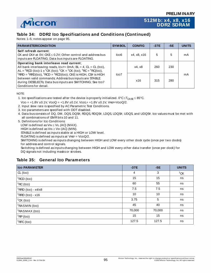
512Mb: x4, x8, x16DDR2 SDRAM
PRELIMINARY
NOTE:
1. IDD specifications are tested after the device is properly initialized. 0°C ≤TCASE ≤ 85°C.VDD = +1.8V ±0.1V, VDDQ = +1.8V ±0.1V, VDDL= +1.8V ±0.1V, VREF=VDDQ/2.
2. Input slew rate is specified by AC Parametric Test Conditions.3. IDD parameters are specified with ODT disabled.4. Data bus consists of DQ, DM, DQS, DQS#, RDQS, RDQS#, LDQS, LDQS#, UDQS, and UDQS#. IDD values must be met with
all combinations of EMR bits 10 and 11.5. Definitions for IDD Conditions:
LOW is defined as VIN ≤ VIL (AC) (MAX).HIGH is defined as VIN ≥ VIH (AC) (MIN).STABLE is defined as inputs stable at a HIGH or LOW level.FLOATING is defined as inputs at VREF = VDDQ/2.SWITCHING is defined as inputs changing between HIGH and LOW every other clock cycle (once per two clocks) for address and control signals. Switching is defined as inputs changing between HIGH and LOW every other data transfer (once per clock) for DQ signals not including masks or strobes.
Self refresh current;CK and CK# at 0V; CKE ≤ 0.2V; Other control and address bus inputs are FLOATING; Data bus inputs are FLOATING.
IDD6 x4, x8, x16 5 5 mA
Operating bank interleave read current;All bank interleaving reads, IOUT= 0mA; BL = 4, CL = CL (IDD), AL = tRCD (IDD)-1 x tCK (IDD); tCK = tCK (IDD), tRC = tRC(IDD), tRRD = tRRD(IDD), tRCD = tRCD(IDD); CKE is HIGH, CS# is HIGH between valid commands; Address bus inputs are STABLE during DESELECTs; Data bus inputs are SWITCHING; See IDD7 Conditions for detail.
IDD7
x4, x8 260 230
mA
x16 315 280
Table 34: DDR2 IDD Specifications and Conditions (Continued)Notes: 1–5; notes appear on page 95.
PARAMETER/CONDITION SYMBOL CONFIG -37E -5E UNITS
Table 35: General IDD Parameters
IDD PARAMETER -37E -5E UNITS
CL (IDD) 4 3 tCKtRCD (IDD) 15 15 ns
tRC (IDD) 60 55 ns
tRRD (IDD) - x4/x8 7.5 7.5 ns
tRRD (IDD) - x16 10 10 ns
tCK (IDD) 3.75 5 ns
tRAS MIN (IDD) 45 40 ns
tRAS MAX (IDD) 70,000 70,000 ns
tRP (IDD) 15 15 ns
tRFC (IDD) 127.5 127.5 ns
09005aef80b88542 Micron Technology, Inc., reserves the right to change products or specifications without notice.512Mb_DDR2_2.fm - Rev. B 7/04 EN 95 ©2003 Micron Technology, Inc. All rights reserved.

512Mb: x4, x8, x16DDR2 SDRAM
PRELIMINARY
IDD7 ConditionsThe detailed timings are shown below for IDD7.
Changes will be required if timing parameter changesare made to the specification.
NOTE:
1. Legend: A = active; RA = read auto precharge; D = deselect.
2. All banks are being interleaved at minimum tRC (IDD) without violating tRRD (IDD) using a burst length of 4.3. Control and address bus inputs are STABLE during DESELECTs.4. IOUT = 0mA.
Table 36: IDD7 Timing PatternsAll Bank Interleave Read operation
SPEED GRADE IDD7 TIMING PATTERNS FOR x4/x8/x16
-5E A0 RA0 A1 RA1 A2 RA2 A3 RA3 D D D D
-37E A0 RA0 D A1 RA1 D A2 RA2 D A3 RA3 D D D D D
09005aef80b88542 Micron Technology, Inc., reserves the right to change products or specifications without notice.512Mb_DDR2_2.fm - Rev. B 7/04 EN 96 ©2003 Micron Technology, Inc. All rights reserved.

512Mb: x4, x8, x16DDR2 SDRAM
PRELIMINARY
Table 37: AC Operating Conditions (Sheet 1 of 4)Notes: 1–5; notes appear on page 101; 0°C ≤ Tcase ≤ +85°C; VDDQ = +1.8V ±0.1V, VDD = +1.8V ±0.1V
AC CHARACTERISTICS -37E -5E
PARAMETER SYMBOL MIN MAX MIN MAX UNITS NOTES
Clo
ck
Clock cycle time
CL = 4 tCK (4) 3,750 8,000 5,000 8,000 ps 16, 25
CL = 3 tCK (3) 5,000 8,000 5,000 8,000 ps 16, 25
CK high-level width tCH 0.45 0.55 0.45 0.55 tCK 19
CK low-level width tCL 0.45 0.55 0.45 0.55 tCK 19
Half clock period tHPMIN
(tCH, tCL)MIN (tCH,
tCL)ps 20
Clock jitter tJIT TBD TBD TBD TBD ps 18
Da
ta
DQ output access time from CK/CK#
tAC -500 +500 -600 +600 ps
Data-out high-impedance window from CK/CK#
tHZ tAC MAX tAC MAX ps 8, 9
Data-out low-impedance window from CK/CK#
tLZ tAC MIN tAC MAX tAC MIN tAC MAX ps 8, 10
DQ and DM input setup time relative to DQS
tDSa 350 400 ps 7, 15, 22
DQ and DM input hold time relative to DQS
tDHa 350 400 ps 7, 15, 22
DQ and DM input setup time relative to DQS
tDSb 100 150 ps 7, 15, 22
DQ and DM input hold time relative to DQS
tDHb 225 275 ps 7, 15, 22
DQ and DM input pulse width (for each input)
tDIPW 0.35 0.35 tCK
Data hold skew factor tQHS 400 450 ps
DQ–DQS hold, DQS to first DQ to go nonvalid, per access
tQH tHP -tQHS tHP -tQHS ps 15, 17
Data valid output window (DVW)
tDVWtQH -
tDQSQ
tQH - tDQSQ
ns 15, 17
09005aef80b88542 Micron Technology, Inc., reserves the right to change products or specifications without notice.512Mb_DDR2_2.fm - Rev. B 7/04 EN 97 ©2003 Micron Technology, Inc. All rights reserved.

512Mb: x4, x8, x16DDR2 SDRAM
PRELIMINARY
Data
Str
ob
e
DQS input high pulse width tDQSH 0.35 0.35 tCK
DQS input low pulse width tDQSL 0.35 0.35 tCKDQS output access time from CK/CK#
tDQSCK -450 +450 -500 +500 ps
DQS falling edge to CK rising – setup time
tDSS 0.2 0.2 tCK
DQS falling edge from CK rising – hold time
tDSH 0.2 0.2 tCK
DQS–DQ skew, DQS to last DQ valid, per group, per access
tDQSQ 300 350 ps 15, 17
DQS read preamble tRPRE 0.9 1.1 0.9 1.1 tCK 36
DQS read postamble tRPST 0.4 0.6 0.4 0.6 tCK 36
DQS write preamble setup time
tWPRES 0 0 ps 12, 13
DQS write preamble tWPRE 0.25 0.25 tCK
DQS write postamble tWPST 0.4 0.6 0.4 0.6 tCK 11
Write command to first DQS latching transition
tDQSS WL - 0.25 WL + 0.25 WL - 0.25 WL + 0.25 tCK
Table 37: AC Operating Conditions (Sheet 2 of 4)Notes: 1–5; notes appear on page 101; 0°C ≤ Tcase ≤ +85°C; VDDQ = +1.8V ±0.1V, VDD = +1.8V ±0.1V
AC CHARACTERISTICS -37E -5E
PARAMETER SYMBOL MIN MAX MIN MAX UNITS NOTES
09005aef80b88542 Micron Technology, Inc., reserves the right to change products or specifications without notice.512Mb_DDR2_2.fm - Rev. B 7/04 EN 98 ©2003 Micron Technology, Inc. All rights reserved.

512Mb: x4, x8, x16DDR2 SDRAM
PRELIMINARY
Com
man
d a
nd
Ad
dre
ss
Address and control input pulse width for each input
tIPW 0.6 0.6 tCK
Address and control input setup time
tISa 500 600 6, 22
Address and control input hold time
tIHa 500 600 6, 22
Address and control input setup time
tISb 250 350 6, 22
Address and control input hold time
tIHb 375 475 6, 22
CAS# to CAS# command delay
tCCD 2 2 tCK
ACTIVE to ACTIVE (same bank) command
tRC 55 55 ns 34
ACTIVE bank a to ACTIVE bank b command
tRRD(x4, x8)
7.5 7.5 ns 28
tRRD (x16) 10 10 ns 28
ACTIVE to READ or WRITE delay
tRCD 15 15 ns
Four Bank Activate periodtFAW
(x4, x8)37.5 37.5 ns 31
Four Bank Activate period tFAW (x16) 50 50 ns 31
ACTIVE to PRECHARGE command
tRAS 40 70,000 40 70,000 ns 21, 34
Internal READ to precharge command delay
tRTP 7.5 7.5 ns 24, 28
Write recovery time tWR 15 15 ns 28
Auto precharge write recovery + precharge time
tDAL tWR + tRP tWR + tRP ns 23
Internal WRITE to READ command delay
tWTR 7.5 10 ns 28
PRECHARGE command period
tRP 15 15 ns 32
PRECHARGE ALL command period
tRPA tRP + tCK tRP + tCK ns 32
LOAD MODE command cycle time
tMRD 2 2 tCK
CKE low to CK,CK# uncertainty
tDELAY 4.375 4.375 5.83 5.83 ns 29
Refr
esh REFRESH to Active or Refresh
to Refresh command intervaltRFC 105 70,000 105 70,000 ns 14
Average periodic refresh interval
tREFI 7.8 7.8 µs 14
Table 37: AC Operating Conditions (Sheet 3 of 4)Notes: 1–5; notes appear on page 101; 0°C ≤ Tcase ≤ +85°C; VDDQ = +1.8V ±0.1V, VDD = +1.8V ±0.1V
AC CHARACTERISTICS -37E -5E
PARAMETER SYMBOL MIN MAX MIN MAX UNITS NOTES
09005aef80b88542 Micron Technology, Inc., reserves the right to change products or specifications without notice.512Mb_DDR2_2.fm - Rev. B 7/04 EN 99 ©2003 Micron Technology, Inc. All rights reserved.

512Mb: x4, x8, x16DDR2 SDRAM
PRELIMINARY
Self R
efr
esh
Exit self refresh to non-READ command
tXSNRtRFC
(MIN) + 10
tRFC(MIN) + 10
ns
Exit self refresh to READ command
tXSRD 200 200 tCK
Exit self refresh timing reference
tISXR 250 350 ps 6, 30
OD
T
ODT turn-on delay tAOND 2 2 2 2 tCK
ODT turn-on tAONtAC
(MIN)
tAC(MAX) +
1,000
tAC (MIN)tAC (MAX)
+ 1000ps 26
ODT turn-off delay tAOFD 2.5 2.5 2.5 2.5 tCK
ODT turn-off tAOFtAC
(MIN)
tAC(MAX) +
600
tAC (MIN)tAC (MAX)
+ 600ps 27
ODT turn-on (power-down mode)
tAONPD
tAC(MIN) +
2000
2 x tCK + tAC
(MAX) + 1,000
tAC(MIN) + 2,000
2 x tCK + tAC
(MAX) + 1000
ps
ODT turn-off (power-down mode)
tAOFPDtAC (MIN)
+ 2,000
2.5 x tCK + tAC (MAX)
+ 1,000
tAC (MIN) + 2,000
2.5 x tCK + tAC
(MAX) + 1,000
ps
ODT to power-down entry latency
tANPD 3 3 tCK
ODT power-down exit latency
tAXPD 8 8 tCK
Po
we
r-D
ow
n
Exit active power-down to READ command, MR[bit12=0]
tXARD 2 2 tCK
Exit active power-down to READ command, MR[bit12=1]
tXARDS 6 - AL 6 - AL tCK
Exit precharge power-down to any non-READ command.
tXP 2 2 tCK
Exit precharge power-down to READ command.
tXPRD 6 - AL 6 - AL tCK
CKE minimum high/low time tCKE 3 3 tCK 35
Table 37: AC Operating Conditions (Sheet 4 of 4)Notes: 1–5; notes appear on page 101; 0°C ≤ Tcase ≤ +85°C; VDDQ = +1.8V ±0.1V, VDD = +1.8V ±0.1V
AC CHARACTERISTICS -37E -5E
PARAMETER SYMBOL MIN MAX MIN MAX UNITS NOTES
09005aef80b88542 Micron Technology, Inc., reserves the right to change products or specifications without notice.512Mb_DDR2_2.fm - Rev. B 7/04 EN 100 ©2003 Micron Technology, Inc. All rights reserved.

512Mb: x4, x8, x16DDR2 SDRAM
PRELIMINARY
Notes1. All voltages referenced to VSS.2. Tests for AC timing, IDD, and electrical AC and DC
characteristics may be conducted at nominal ref-erence/supply voltage levels, but the related spec-ifications and device operation are guaranteed forthe full voltage range specified.
3. Outputs measured with equivalent load:
4. AC timing and IDD tests may use a VIL-to-VIH swingof up to 1.0V in the test environment and parame-ter specifications are guaranteed for the specifiedAC input levels under normal use conditions. Theminimum slew rate for the input signals used totest the device is 1.0V/ns for signals in the rangebetween VIL (AC) and VIH (AC). Slew rates lessthan 1.0V/ns require the timing parameters to bederated as specified.
5. The AC and DC input level specifications are asdefined in the SSTL_18 standard (i.e., the receiverwill effectively switch as a result of the signalcrossing the AC input level and will remain in thatstate as long as the signal does not ring backabove [below] the DC input LOW [HIGH] level).
6. Command/Address minimum input slew rate is at1.0V/ns. Command/Address input timing must bederated if the slew rate is not 1.0V/ns. This is eas-ily accommodated using tISb and the Setup and
Hold Time Derating Values table. tIS timing (tISb)is referenced from VIH(AC) for a rising signal and
VIL(AC) for a falling signal. tIH timing (tIHb) is refer-enced from VIH(AC) for a rising signal and VIL(DC)for a falling signal. The timing table also lists thetISb and tIHb values for a 1.0V/ns slew rate; theseare the “base” values.
7. Data minimum input slew rate is at 1.0V/ns. Datainput timing must be derated if the slew rate is not1.0V/ns. This is easily accommodated if the tim-
ing is referenced from the logic trip points. tDStiming (tDSb) is referenced from VIH(AC) for a ris-
ing signal and VIL(AC) for a falling signal. tIH tim-ing (tIHb) is referenced from VIH(DC) for a risingsignal and VIL(DC) for a falling signal. The timingtable lists the tDSb and tDHb values for a 1.0V/nsslew rate.
If the DQS/DQS# differential strobe feature is notenabled, timing is no longer referenced to thecrosspoint of DQS/DQS#. Data timing is now ref-erenced to VREF, provided the DQS slew rate is notless than 1.0V/ns. If the DQS slew rate is less than1.0V/ns, then data timing is now referenced toVIH(AC) for a rising DQS and VIL(DC) for a fallingDQS.
8. tHZ and tLZ transitions occur in the same accesstime windows as valid data transitions. Theseparameters are not referenced to a specific voltagelevel, but specify when the device output is no
longer driving (tHZ) or begins driving (tLZ).9. This maximum value is derived from the refer-
enced test load. tHZ (MAX) will prevail overtDQSCK (MAX) + tRPST (MAX) condition.
10. tLZ (MIN) will prevail over a tDQSCK (MIN) +tRPRE (MAX) condition.
11. The intent of the Don’t Care state after completionof the postamble is the DQS-driven signal shouldeither be high, low or High-Z and that any signaltransition within the input switching region mustfollow valid input requirements. That is if DQStransitions high (above VIHDC(min) then it mustnot transition low (below VIH(DC) prior totDQSH(min).
12. This is not a device limit. The device will operatewith a negative value, but system performancecould be degraded due to bus turnaround.
13. It is recommended that DQS be valid (HIGH orLOW) on or before the WRITE command. Thecase shown (DQS going from High-Z to logicLOW) applies when no WRITEs were previously inprogress on the bus. If a previous WRITE was inprogress, DQS could be HIGH during this time,
depending on tDQSS.14. The refresh period is 64ms. This equates to an
average refresh rate of 7.8125µs. However, aREFRESH command must be asserted at least
once every 70.3µs or tRFC (MAX). To ensure allrows of all banks are properly refreshed, 8192REFRESH commands must be issued every 64ms.
15. Referenced to each output group: x4 = DQS withDQ0-DQ3; x8 = DQS with DQ0–DQ7; x16 = LDQSwith DQ0–DQ7; and UDQS with DQ8–DQ15.
16. CK and CK# input slew rate must be ≥ 1V/ns (≥ 2V/ns if measured differentially).
17. The data valid window is derived by achieving
other specifications - tHP. (tCK/2), tDQSQ, and
Output(VOUT)
Reference Point
25Ω
VTT = VDDQ/2
09005aef80b88542 Micron Technology, Inc., reserves the right to change products or specifications without notice.512Mb_DDR2_2.fm - Rev. B 7/04 EN 101 ©2003 Micron Technology, Inc. All rights reserved.

512Mb: x4, x8, x16DDR2 SDRAM
PRELIMINARY
tQH(tQH=tHP-tQHS). The data valid window der-ates in direct proportion to the clock duty cycleand a practical data valid window can be derived.
18. tJIT specification is currently TBD.
19. MIN(tCL, tCH) refers to the smaller of the actualclock low time and the actual clock high time asprovided to the device (i.e. This value can begreater than the minimum specification limits fortCL and tCH). For example, tCL and tCH are = 50percent of the period, less the half period jitter
[tJIT(HP)] of the clock source, and less the half
period jitter due to cross talk [tJIT(cross talk)] intothe clock traces.
20. tHP (MIN) is the lesser of tCL minimum and tCHminimum actually applied to the device CK andCK# inputs.
21. READs and WRITEs with auto precharge are
allowed to be issued before tRAS (MIN) is satisfied
since tRAS lockout feature is supported in DDR2SDRAM.
22. VIL/VIH DDR2 overshoot/undershoot. See “ACOvershoot/Undershoot Specification” on page 88.
23. tDAL = (nWR) + (tRP/tCK): For each of the termsabove, if not already an integer, round to the next
highest integer. tCK refers to the application clock
period; nWR refers to the tWR parameter stored in
the MR[11,10,9]. Example: For -37E at tCK = 3.75
ns with tWR programmed to four clocks. tDAL = 4+ (15 ns/3.75 ns) clocks = 4 +(4) clocks = 8 clocks.
24. The minimum READ to internal PRECHARGEtime. This parameter is only applicable whentRTP/(2*tCK) > 1. If tRTP/(2*tCK) ≤ 1, then equa-
tion AL + BL/2 applies. Notwithstanding, tRAS(MIN) has to be satisfied as well. The DDR2SDRAM will automatically delay the internal PRE-
CHARGE command until tRAS (MIN) has beensatisfied.
25. Operating frequency is only allowed to changeduring self refresh mode (See “Self Refresh” onpage 34), precharge power-down mode (See“Power-Down Mode” on page 37), and systemreset condition (see “RESET Function (CKE LOWAnytime)” on page 8.
26. ODT turn-on time tAON (MIN) is when the deviceleaves high impedance and ODT resistance
begins to turn on. ODT turn-on time tAON (MAX)is when the ODT resistance is fully on. Both are
measured from tAOND.
27. ODT turn-off time tAOF (MIN) is when the devicestarts to turn off ODT resistance. ODT turn off
time tAOF (MAX) is when the bus is in high
impedance. Both are measured from tAOFD.28. This parameter has a two clock minimum require-
ment at any tCK.
29. tDELAY is calculated from tIS + tCK + tIH so thatCKE registration LOW is guaranteed prior to CK,CK# being removed in a system RESET condition.“RESET Function (CKE LOW Anytime)” on page 8.
30. tISXR is equal to tIS and is used for CKE setup timeduring self refresh exit shown in Figure 31 onpage 36.
31. No more than 4 bank ACTIVE commands may be
issued in a given tFAW(min) period. tRRD(min)
restriction still applies. The tFAW(min) parameterapplies to all 8 bank DDR2 devices, regardless ofthe number of banks already open or closed.
32. tRPA timing applies when the PRECHARGE(ALL)command is issued, regardless of the number ofbanks already open or closed. If a single-bank
PRECHARGE command is issued, tRP timing
applies. tRPA(min) applies to all 8-bank DDR2devices.
33. Value is minimum pulse width, not the number ofclock registrations.
34. Applicable to Read cycles only. Write cycles gener-ally require additional time due to Write recovery
time (tWR) during auto precharge.
35. tCKE (MIN) of 3 clocks means CKE must be regis-tered on three consecutive positive clock edges.CKE must remain at the valid input level the entiretime it takes to achieve the 3 clocks of registration.Thus, after any CKE transition, CKE may not tran-sition from its valid level during the time period oftIS + 2 * tCK + tIH.
36. This parameter is not referenced to a specific volt-age level, but specified whwen the device output
is no longer driving (tRPST) or beginning to drive
(tRPRE).
09005aef80b88542 Micron Technology, Inc., reserves the right to change products or specifications without notice.512Mb_DDR2_2.fm - Rev. B 7/04 EN 102 ©2003 Micron Technology, Inc. All rights reserved.

512Mb: x4, x8, x16DDR2 SDRAM
PRELIMINARY
®
8000 S. Federal Way, P.O. Box 6, Boise, ID 83707-0006, Tel: 208-368-3900E-mail: [email protected], Internet: http://www.micron.com, Customer Comment Line: 800-932-4992
Micron, the M logo, and the Micron logo are trademarks of Micron Technology, Inc. All other trademarks are the property of their respective owners.
Figure 85: Package Drawing (x4,x8,x16 Configurations) 11mm x 19mm FBGA
NOTE:
All dimensions are in millimeters.
Data Sheet DesignationPreliminary: Initial characterization limits, subject
to change upon full characterization of productiondevices.
BALL A1 ID
SUBSTRATE: PLASTIC LAMINATE
MOLD COMPOUND: EPOXY NOVOLAC
SOLDER BALL MATERIAL: 96.5% SN, 3% AG, 0.5% CUSOLDER BALL PAD: Ø 0.33mm; SOLDER BALL DIAMETER REFERS TO POST REFLOW CONDITION. THE PRE-REFLOWDIAMETER IS Ø 0.42
SEATING PLANE
0.850 ±0.075
BALL A9
0.08 CC
C
0.100 ±0.013
0.80TYP
16.00
1.20 MAX
8.00 ±0.05
9.50 ±0.05
1.80 ±0.05CTR
BALL A1 IDBALL A1
0.80TYP
5.50 ±0.053.20 ±0.05
11.00 ±0.10
6.400.4592X Ø
C L
C L
19.00 ±0.10
09005aef80b88542 Micron Technology, Inc., reserves the right to change products or specifications without notice.512Mb_DDR2_2.fm - Rev. B 7/04 EN 103 ©2003 Micron Technology, Inc. All rights reserved.