preamplifiers for electro-optic detectors · 3 figure 1 transimpedance preamplifier for...
TRANSCRIPT
1
PREAMPLIFIERS FOR ELECTRO-OPTIC DETECTORS
copyright 1998-2009 Everett Companies LLC
INTRODUCTION
Basically there two types of electro-optic detectors, those made from semiconductors and those that are not. The main difference is that a semiconductor detector is governed primarily by the energy gap between the valence and conduction bands and non-semiconductor detectors do not have bandgaps. Physics of Electro-optic Detectors has a discussion of how both semiconductor and non-semiconductor electro-optic detectors work. Semiconductor detectors are frequently referred to as quantum detectors and non-semiconductor detectors as thermal detectors. See Physics of Electro-optic Detectors for the reasons behind these designations.
The two common types of semiconductor detectors are photoconductors and photodiodes. The more common non-semiconductor detectors are bolometers, thermopiles and pyroelectric detectors. Preamplifiers for all of these detectors are discussed below.
Electro-optic detectors are used individually to detect the presence of radiation and measure its intensity or in arrays to additionally provide spatial resolution such as in an imager or spectrometer. The electronics interfaced to a large detector array are usually in the form of an application specific integrated circuit (ASIC) designed for that purpose. The electronics for individual detectors and small arrays are usually made up of discrete components placed on a printed circuit board. In either case the preamplifiers that connect directly to the detectors are basically the same although the implementations may differ.

2
The preamplifiers described below are the basic circuits for extracting useful signals from the detectors, and they will provide a more than usable signal in most cases. However, as in most things, the devil is in the details. Substantially improved performance can be achieved by designing the preamplifiers and the following circuitry to meet the requirements of the specific application. Doing this requires a level of depth and detail beyond what can be covered here. Also, substantial signal processing electronics frequently follow the preamplifiers. These signal processing electronics are often digital incorporating microprocessors and are also not discussed.
The preamplifiers described below are set-up for bipolar operation and require dual power supplies. It is, however, straightforward to convert them to monopolar operation requiring only a single power supply (e.g. +5 V).
PREAMPLIFIERS FOR PHOTOCONDUCTORS
Photoconductors are usually used only for infrared detection while photodiodes are used for all wavelengths. A photoconductive detector is doped to have a finite conductivity. When a bias is applied to the detector in the absence of radiation, a current is generated that is called the dark current. When the material is exposed to radiation with wavelength short enough to bridge the bandgap, additional charge carriers are generated and the current is increased. The photosignal is this increase in the current caused by the radiation. The photosignal is typically much smaller than the dark current, usually on the order of a few parts in a thousand. Extracting this small signal from the much larger dark current is the primary task of the preamplifier.
There are two types of preamplifiers for photoconductors, voltage mode amplifiers and current mode or transimpedance amplifiers. The basic transimpedance amplifier is shown in Figure 1. The operational amplifier's non-inverting input is connected to ground with resistance Rgnd selected to minimize the amplifier's dc offset. The detector, Rdet, is biased by a power supply to voltage Vbias. Since the other end of the detector is held at virtual ground by the operational amplifier, the current through the detector is
I = Vbias/Rdet
This current flows through the feedback resistor Rf, and the output voltage is

3
Figure 1 Transimpedance preamplifier for photoconductive detectors
Vout = -(Rf/Rdet)Vbias
The detector bias voltage is usually large, and the Zener diode (D) with a breakdown voltage of a volt or so has been added to protect the operational amplifier and can actually be installed in either direction. A regular diode can be used in its place, but then the polarity with which it is connected does make a difference. The responsivity of a photoconductive detector is a function of the electric field within the detector material, and each detector has an optimum bias, although the performance peak is usually fairly broad. Many photoconductive detectors require bias voltages as high as 50 V or more to achieve optimum performance. The inverting input of the first stage amplifier is normally at virtual ground. However if leads are broken or inadvertently not connected, the input could be exposed to Vbias which can damage many operational amplifiers. The

4
diode can be deleted if Vbias is below the rated maximum input voltage for the operational amplifier being used.
In principle, the dark current can be separated from the photogenerated signal by simply subtracting it. The detector has a well defined dark resistance, and the dark current is given by
Idark = Vbias/Rdark
Since the total detector current is simply
Itotal = Isignal + Idark
subtracting the dark current directly yields the signal. The problem comes about because Rdark is a strong function of detector temperature In addition to incident radiation, valence electrons can be excited to the conduction band by thermal agitation, phonons (see Physics of Electro-optic Detectors for an explanation). A small increase in the detector temperature will generate a large number of additional charge carriers and, in general, overwhelm the photogenerated signal. To keep this from happening, the detector temperature must be controlled to something on the order 0.01 oC or better. Usually this is not feasible, and the subtraction method is not a reliable way to extract the signal from the background.
The most commonly used method to extract the signal is to modulate the incident radiation at a specific frequency. The optically generated signal then is modulated at this frequency while the slowly changing dark current remains near dc. This is often done by placing a mechanical chopper in front of the detector. In some applications the radiation source or emitter can be electrically modulated instead. It is relatively straightforward to use ac coupling to separate the ac signal from the near dc background.
The transimpedance amplifier is inherently dc coupled. Therefore, a second ac coupled stage must be used to remove the dark current. This is shown in Figure 2. The first stage output contains both the signal and the dark current, and the transimpedance gain must be small enough so that the amplifier does not saturate.

5
The first stage output is ac coupled to the second stage. The first stage output signal is inversely proportional to Rdet which in turn is directly proportional to the irradiance, the intensity of the incident radiation. The irradiance is the optical power per unit area incident on the detector and is usually given in units of W/cm2.
Figure 2 Two stage ac coupled transimpedance preamplifier for photoconductive detectors
Rdet = Rdark – cH

6
where Rdark is the detector resistance in the absence of radiation, c is constant (which includes the detector area) and H is the irradiance. The optical power incident on the detector is
Pdet = AdetH
where Adet is the optically sensitive area of the detector. Since Rdark >> cH
V1out = -(R1Vbias/Rdark)(1 + cH/Rdark)
to first order. The second stage gain is actually
G2 = [(R2 + R3)Rgnd2]/[R2(Rgnd22 + (2πfCinput)
-2)1/2]
If the components are selected so that Rgnd2 >> (2πfCinput)-1
G2 = (R2 + R3)/R2
Only the ac portion of V1out is passed to the second stage amplifier and
V2out = [R1/Rdark2 ][(R2 + R3)/R2]cHVbias
Since V2out is ac, the minus sign is not really useful and has been dropped. The output signal is directly proportional to the irradiance which makes calibration very straightforward. The constant c is given by

7
c = RAdet
where R is the detector responsivity in Ω/W assuming H has the units of W/cm2
and Adet is the optically sensitive area of the detector surface and has the units of cm2. The responsivity is usually given by detector manufacturers in volts per watt and must be converted into ohms per watt. One should be careful since a photoconductor responsivity value quoted in volts per watt depends on the way in which it was measured. In any case, the physically meaningful quantity is the dependence of the detector resistance on incident optical power.
An advantage of the voltage mode preamplifier is that the signal can be extracted with a single stage. This is illustrated in Figure 3. A series combination of the detector, Rdet, and a load resistor, Rload, is biased by a power supply to Vbias. The current through the detector and load resistor is
Figure 3 Voltage mode preamplifier for photoconductive detectors

8
I = Vbias/(Rdet + Rload)
and the signal generated across Rload is
Vload = VbiasRload/(Rdet + Rload)
This signal is ac coupled to the non-inverting input of the operational amplifier. If the component values are selected so that
Rload << Rgnd >> [2πfCinput]-1
the amplifier gain is independent of frequency and
Vout = [Rload/(Rdark + Rload)2][(R1 + R2)/R1]cHVbias
Again, the output signal is proportional to the irradiance to first order. The positions of the detector and load resistor can be exchanged without effect, again to first order, other than a phase change in the output signal. The maximum signal is achieved when Rload = Rdark and falls off whenever Rload is either larger or smaller than Rdark.
The operating point of the photoconductive detector should be placed at or near the peak responsivity by selecting the appropriate value for Vbias. Since the capacitor blocks dc from the operational amplifier input, a protection diode is not needed for the preamplifier shown in Figure 3.
A disadvantage of the voltage modes is that Vbias is generally twice that needed for the detector itself. This is often an issue since the optimum detector bias is usually fairly high to start with.
Historically, there has been a spirited discussion of whether it is better to use a transimpedance amplifier of the type shown in Figure 2 or a voltage mode

9
amplifier such as that shown in Figure 3. In the end, the two provide essentially the same general level of performance. Voltage mode detection requires only one amplifier stage while transimpedance detection requires two stages. However, the two amplifier stages provide a better opportunity for noise reduction as well as the reduced Vbias requirement, and marginally better performance can usually be achieved with transimpedance detection. Which is the better choice really depends on the details of the application and the preference of the user.
PREAMPLIFIERS FOR PHOTODIODES
The I-V characteristic for a photodiode is shown in Figure 4. In the absence of radiation the curve goes through the origin. When the detector is exposed to radiation with sufficiently short wavelength to bridge the bandgap, a potential is generated across the junction and the curve is shifted downward as shown in the figure. The place where the shifted I-V curve crosses the voltage axis is called the open circuit voltage, Voc. The place where it crosses the current axis is called the short circuit current, Isc.
Photodiodes can be operated in the short circuit condition, where the bias across the detector is held at or near zero using a simple transimpedance amplifier. In principle, however, this does not result in the best performance, at least for narrow bandgap detectors. That is achieved when a small reverse bias is applied to the detector. The reasons for this are discussed below. The preamplifier shown in Figure 5 applies bias Vref to the photodiode. The short circuit current is proportional to the radiation intensity.
Isc = RAdetH
where R is the detector responsivity in A/W, H is the irradiance (intensity) in W/cm2 and, as above, Adet is the optically active area of the detector in cm2. Since the I-V curve maintains its shape, the total detector current is the sum of the radiation generated short circuit current and the bias generated dark current.
Idet = Isc + Idark
Since the amplifier output is proportional to the detector current
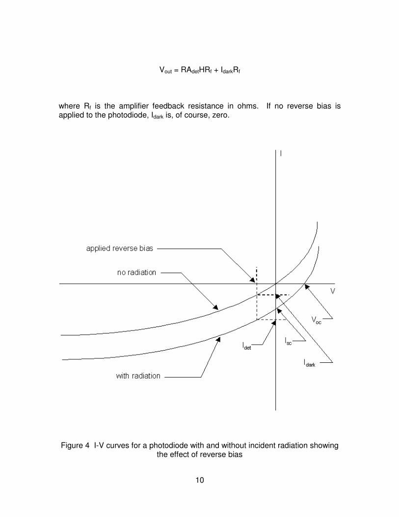
10
Vout = RAdetHRf + IdarkRf
where Rf is the amplifier feedback resistance in ohms. If no reverse bias is applied to the photodiode, Idark is, of course, zero.
Figure 4 I-V curves for a photodiode with and without incident radiation showing the effect of reverse bias

11
Figure 5 Transimpedance preamplifier for photodiodes
Noise is normally contributed by three sources: the incident radiation, the detector and the electronics. While the noise generated in wide bandgap detectors can frequently be neglected, this is not usually the case with narrow bandgap infrared detectors. The noise from the electronics is usually small enough that it can also be neglected except in cases where the radiation intensity is very low. The condition when both the detector noise and the electronics noise can be neglected and the total noise is effectively that inherent in the radiation itself is called the background limit, the highest level of performance possible. Separate from the dark current, the detector noise contribution decreases as the detector impedance increases. Applying a reverse bias decreases the slope of the I-V curve increasing the detector's dynamic impedance and decreasing its Johnson noise. However, the added dark current contains shot noise. Optimum performance is achieved when the noise reduction from the increased impedance equals the noise increase from the dark current. If the quadrature

12
sum of these two noise components and whatever electronics noise there is can be neglected compared to the radiation noise, background limited performance has been achieved.
The detector noise contribution increases as the band gap decreases. Wider
band gap detectors, those sensitive to 5 µm wavelengths and shorter, usually have sufficiently low noise that it can be neglected at zero bias except in cases where the intensity of the incident radiation is very low, and the non-inverting input of the operational amplifier in Figure 5 can be connected to ground. However, this is not the case with photodiodes sensitive to longer wavelengths.
For detection of 10 µm or longer radiation, performance is almost always improved by applying a small reverse bias to the detector. In most cases this is on the order of a few milivolts to perhaps as many as 50 mV.
Background limited performance can be improved by integrating the detector current onto a capacitor and sampling the output. The circuit shown in Figure 6 achieves this. The capacitor Cint is reset to a relatively strong reverse bias, Vreset, by switch Q2. Transistor Q1 controls the flow of current from the detector. Operational amplifier A1 maintains the detector at reverse bias Vref by applying just enough bias to the gate of Q1. The detector current is integrated on Cint for
as long as Q2 is open. The integration time is determined by φclock. When φclock closes Q2, Cint is reset, and a new integration period is started when Q2 is again opened. Follower A2 reads the voltage on the capacitor, Vout, which is usually captured by a standard sample-and-hold circuit just before Cint is reset. Since Cint is being discharged by the detector current, Vout is equal to an offset less a term proportional to the irradiance. The noise on the integrated signal increases as the square root of the size of the charge packet integrated on Cint while the signal itself, of course, increases linearly. Therefore, the signal-to-noise ratio is improved by integrating for as long as possible. For constant irradiance, the signal-to-noise ratio in the background limit increases with the square root of the integration time.
The detector can also be operated in the open circuit condition where no current is allowed to flow from the diode. This is accomplished with the circuit shown in Figure 7. In order to maintain the open circuit condition, the input impedance of the operational amplifier must be substantially larger than the shunt resistance of the detector. Because of the exponential nature of the photodiode I-V curve, Vout depends logarithmically on the irradiance.
Vout = [(R1 + R2)/R1]ln[(Isc + Io)/Io]

13
where Io is the photodiode saturation current and the other parameters have already been defined. The open circuit configuration is normally used when the incident radiation varies over a wide range and a logarithmic response is more appropriate than a linear response. A major drawback of this approach is that Io is exponentially dependent on the detector temperature, and this temperature must be very tightly controlled, usually a difficult task. It is for this reason that the open circuit configuration is seldom used.
Figure 6 Integrating preamplifier with controlled bias for photodiodes
PREAMPLIFIERS FOR THERMOPILES
A thermopile is a series combination of something on the order of 20-200 thermocouples. When the two junctions of a thermocouple are held at different

14
temperatures, a small but measurable voltage is generated between them. In a thermopile these individual thermocouple voltages are added together to give a larger signal that can be measured more easily. While a thermocouple can generate a voltage, it cannot supply any substantial current, and if a current is allowed to flow, the voltage will fall rapidly to zero. Therefore, no current of any significant amount can be drawn from a thermopile.
Figure 7 Open circuit preamplifier for photodiodes
The thermopile is fabricated on a substrate that is usually about a millimeter or two in size. One set of thermocouple junctions is thermally isolated and exposed to the incident radiation while the other set is heat sunk to the package. The absorbed radiation causes the temperature of the exposed junctions to increase or decrease as is discussed below and in Physics of Electro-optic Detectors. The amount of temperature increase depends on the irradiance (intensity of the incident radiation) and the thermal conductivity to the ambient. The thermopile signal which is usually on the order of a millivolt or less is proportional to the irradiance, and the responsivity is typically on the order of 10-100 V/W. The thermopile has maximum response at dc, and because the material on which the exposed set of junctions is mounted has a fairly substantial thermal mass and a

15
low thermal conductivity path to the heat sink, the response falls off fairly rapidly with frequency. A typical thermopile can detect radiation modulated at frequencies up to 10 Hz or so but not much higher.
Thermopiles are frequently used to detect unmodulated radiation in such applications as non-contact temperature sensors. The size of the signal generated by the thermopile depends on a laundry list of conditions and can vary from a few tens of microvolts or less to tens of milivolts or more. The preamplifier gain required to generate an output signal on the order of volts can vary from something as small as 10 to something as large as 10,000 or more. In general, gains of more than1,000 are best provided by two amplifier stages while gains less than 1,000 can be handled by a single stage. A two stage preamplifier appropriate for use with a thermopile is shown in Figure 8. The output signal from the first stage is
Figure 8 High input impedance non-inverting dc coupled preamplifier for thermopile detectors
Vout1 = [(R1 + R2)/R1]Vdet

16
where Vdet is the signal generated by the thermopile. Then the output from the second stage is
Vout = [(R1 + R2)/R1][(R3 + R4)/R3]Vdet
If the overall gain is less than 1000, the second stage can simply be deleted.
The thermopile signal, Vdet , will be positive if the temperature of the object filling the thermopile's optical field-of-view is greater than the ambient temperature and negative if the reverse is the case. Needless to say, operational amplifier A1
must have a high input impedance, usually >1012 Ω. Now Vdet = R(Ptarget – Pambient) where Ptarget is the optical power incident on the detector when it is exposed to the radiation coming from the target, Pambient is the optical power that would be incident on the detector if it were exposed to the ambient radiation (see Physics of Electro-optic Detectors for a more complete explanation) and R is the detector responsivity. The optical power is just the optically sensitive area of the detector times the irradiance.
This is how the non-contact temperature sensor works. Ptarget is determined from Vout, the electronics gain, the detector responsivity and Pambient. The ambient temperature must be known in order to calculate Pambient. The temperature of the target surface is then determined from Ptarget usually through a look-up table stored in memory accessible by a microprocessor.
The ambient temperature is frequently not all that uniform, and very accurate measurements may require a more accurate reference. The dependence of the output signal on the ambient temperature can be eliminated by alternately exposing the thermopile to the radiation to be measured and radiation of known intensity. Switching back and forth between the two radiation sources can be accomplished with an oscillating mirror or in a number of other ways. An appropriate preamplifier for this application is shown in Figure 9. The thermopile signal when it is exposed to each of the sources is equal to a term proportional to the radiant power from that source that is incident on the detector minus a term that depends on the ambient temperature but not the incident optical power. The capacitive or ac coupling between the two amplifier stages in Figure 9 allows only the difference signal to pass to the second stage amplifier. That portion of the thermopile signal that is dependent on the ambient temperature is the same when the thermopile is exposed to the two radiation sources and is blocked from passing to the second stage amplifier. The preamplifier output signal then is

17
Vout = gR∆P
where g is the overall preamplifier gain, R is the detector responsivity and ∆P = Pmeas – Pknown. The optical power incident on the detector from the unknown source (Pmeas) can be determined since the incident power from the other source (Pknown) is known. The values of R5 and C, of course, must be selected to match the rate at which the detector is switched from one source to the other so that the difference signal is passed to the second stage amplifier and not blocked along with the ambient temperature terms. Since the response of a thermopile falls off at higher frequencies, the switching rate must be fairly low, typically <5 Hz.
Figure 9 Capactively coupled two stage preamplifier appropriate for difference measurement using a thermopile
Since the thermopile signal is usually small and the preamplifier gain large, the amplifier input offset voltage and bias current can make significant contributions to the output signal in a dc coupled preamplifier such as that shown in Figure 8. These contributions must be taken into account in applications where the absolute value of the sensor output signal is important, such as a remote temperature sensor. The capacitor in the preamplifier shown in Figure 9 blocks the first stage offset from being passed to the second stage amplifier. Offset
18
then is usually not an issue with this type of preamplifier unless the gain of the second stage amplifier is large. This situation can usually be avoided by absorbing as much gain as possible into the first stage.
PREAMPLIFIERS FOR PRYOELECTRIC DETECTORS
Pyroelectric detectors are fabricated by placing electrodes on opposite faces of a crystalline material that is spontaneously electrically polarized and where the degree of polarization changes with temperature. Pyroelectric detectors are made in a manner similar to thermopiles. The detector crystal is a thin wafer that is thermally isolated from the ambient. The front face of the crystal is exposed to the incident radiation. The temperature of the crystal rises and falls in step with the intensity of the incident radiation. The electric dipole moment of the crystal then also changes with the incident radiation, and it is this change in the dipole moment that is detected. A much more complete discussion of pyroelectric detectors is provided in Physics of Electro-optic Detectors.
The spontaneous polarization of the detector material induces a net positive charge on one face of the crystal and a net negative charge on the other. The amount of charge on the crystal faces is small and is fairly quickly neutralized by deposition of ions from the surrounding atmosphere or by electrical conduction. Pyroelectric detectors, therefore, can only be used to detect modulated radiation, and the modulation must be fast enough that the neutralization of the surface charge can't keep up. These detectors can be operated in either the voltage mode or the current mode, and one mode or the other will be more appropriate depending on the application. In the voltage mode, it is the voltage generated across the entire pyroelectric crystal that is detected. The incident radiation is absorbed on the exposed or top surface of the crystal. The thermal energy is conducted through the crystal to the back or bottom face bringing the entire crystal to a roughly uniform temperature. The crystal is more or less uniformly polarized with net positive charge on one crystal face and net negative charge on the other. Clearly, voltage mode detection can only be used at modulation frequencies low enough so that the thermal energy has enough time to be conducted through the crystal before the incident radiation starts back the other way. Current mode detection is appropriate for high frequency modulation where the temperature of only a relatively thin layer of the crystal at the exposed surface is affected by the incident radiation. The modulation frequency is fast enough that the thermal energy is not conducted into the bulk of the crystal. Since the absorbed energy is not distributed over the bulk of the crystal, the temperature excursions of the crystal material immediately adjacent to the exposed face are maximized as is the charge generated on the exposed face. In current mode operation, it is the current flowing on and off the electrode on the exposed face of the crystal that is detected. The temperature at the back surface
19
of the detector and the charge on that surface doesn't change at the high modulation frequencies used for current mode detection.
In voltage mode operation, the amount of surface charge generated on a pyroelectric detector by the incident radiation is typically quite small. The detector is basically a capacitor with a shunt or leakage resistance. A typical pyroelectric detector will have a capacitance on the order of 10 pF or more and a
shunt resistance typically greater than 1012 Ω. The responsivity of a typical pyroelectric detector operated in the voltage mode peaks for modulation frequencies somewhere in the 0.01-0.1 Hz range. It falls off at lower frequencies due to discharging or neutralization of the surface charge and at higher frequencies due to the thermal mass of the crystal. A preamplifier, of course, necessarily provides an additional parallel shunt path for neutralization of the surface charge, and the resistance of that path must be greater or at least not smaller than the shunt resistance of the detector itself if it is not to significantly reduce the detector signal and degrade performance.
A preamplifier for voltage mode detection is shown in Figure 10. Operational
amplifiers are available with input impedances of 1012 Ω and often as high as
1014 Ω. The preamplifier shown in Figure 10 with a high input impedance operational amplifier provides the highest detection sensitivity possible. However, this configuration suffers from instability caused by ambient temperature drift. The polarization, of course, changes as the temperature of the crystal changes. Small changes in the ambient temperature then cause the preamplifier output signal to drift up or down. This problem can be avoided by maintaining the detector at a stable ambient temperature. However, it is often very difficult to provide the degree of ambient temperature stability needed. The issue can also be addressed by adding a second stage amplifier as shown in Figure 11. High frequencies are passed to A2 while the low frequencies are not.
The values of R3 and C are chosen so that R3 > 1/(2πfC) where f is the modulation frequency. Then the modulated signal will be passed to the second stage amplifier, but the effect of ambient temperature drift at rates slower than f will be blocked.
Voltage mode pyroelectric detectors are generally available from the manufacturers integrated with a field-effect-transistor (FET) as shown in Figure 12. The FET effectively becomes the first stage amplifier. A power supply and load resistor RL are externally attached to the FET, and the output signal appears across RL. A shunt resistance RS is typically added across the detector to provide thermal stabilization. The values for the shunt resistance are usually in
the range from 1010-1011 Ω. The value of RS should be selected to match the detector capacitance and provide the appropriate time constant. The shunt resistor does provide stability against changes in the ambient temperature but also allows the detector to discharge with the concomitant reduction in detector signal. While integrating an FET and shunt resistor with the detector reduces the amount of additional electronics that are needed, the preamplifier shown in

20
Figure 11 provides a degree of flexibility allowing the appropriate time constant to be selected that best separates ambient temperature drift from the modulated signal without causing unnecessary surface discharge. However, if the detector is exposed to the external world, care will have to be taken to make sure that a significant shunt path is not provided by contamination on the surface of a printed circuit board or whatever. At these resistances, that is not a trivial task.
Figure 10 Simple preamplifier for voltage mode detection with a pyroelectric detector
The impact of ambient temperature drift can also be mitigated by adding a compensation crystal. Two identical pyroelectric crystals are connected in opposition, either in series or in parallel. One of the crystals is exposed to the incident radiation and the other shielded from it. The parallel configuration is illustrated in Figure 13. As the ambient temperature changes, the surface charged generated on one crystal is cancelled by the equal but opposite charge generated on the other crystal. The incident radiation, however, generates charge only on one crystal and is not cancelled. The disadvantage, of course, is that this charge is distributed over twice the capacitance, and the responsivity of a compensated detector is only half that of the equivalent uncompensated

21
detector. Thermally compensated dual crystal detectors are also available integrated with a FET and shunt resistor.
Figure 11 Two stage capactively coupled voltage mode preamplifier that removes the effect of ambient temperature drift
A preamplifier appropriate for current mode detection is shown in Figure 14. The radiation is incident on the exposed crystal face on the top of the detector. The modulation frequency is fast enough that the thermal energy generated by the radiation does not have time to penetrate into the bulk of the crystal and is restricted to a thin layer below the crystal face absorbing the incident radiation. The incident radiation modulates the surface charge on the top face of the crystal but not on the bottom face. The electrode on the bottom face of the crystal is attached to ground. The operational amplifier maintains the electrode on the exposed face at virtual ground, and the current required to neutralize the charge generated on the exposed face flows through R1 generating output voltage V1 at the output of the first stage amplifier. The responsivity R of current mode detectors is given in A/W, and the modulated component of V1 is

22
∆V1 = RR1∆P
Figure 12 Pyroelectric detector integrated with FET and shunt resistor. The FET with the load resistor forms the preamplifier. The shunt resistor provides stability against ambient temperature drift, but its value must be carefully selected.
where ∆P is the modulated component of the incident radiation. In addition to
∆V1, V1 may have a component generated by a drift in the ambient temperature. Current mode detection is made at modulation frequencies high enough that the ambient temperature drift does not mix into the signal generated by the incident radiation and the two are easily separated. Figure 14 shows how this drift component is removed by ac coupling V1 to second stage amplifier as was done in Figure 11. The R2C time constant is chosen to pass the modulated component of V1 but block the drift component.
Thermally compensated dual crystal detectors (without the FET and shunt resistor) can also be operated in the current mode.

23
Figure 13 Parallel configuration of a thermally compensated pyroelectric detector operated in the voltage mode
Figure 14 Two stage preamplifier for a pyroelectric detector operated in the current mode
24
POST PREAMPLIFIER ELECTRONICS
The output signal from the preamplifier is proportional to the optical power incident on the detector in the case of the quantum detector and to the difference in that power and the equivalent ambient power in the case of the thermal detector. Quite often it is enough just to detect the incident radiation, and, in that case, our job is done. However, it is frequently the case that we have to convert this signal to a meaningful measurement. An example is the non-contact or remote temperature sensor. This device captures radiation emitted by an object and converts the detector signal to the object's temperature. As we saw in Physics of Electro-optic Detectors, this is not a trivial task. Basically, we have to go backwards through Planck's Law to get from the detector signal to the emitting surface temperature. The hard number crunching is normally done by a computer and the results put into a form that can be manipulated by a microprocessor. This means that as a minimum an analog-to-digital converter (ADC) and a microprocessor follow the preamplifier, and usually there is quite a bit more.
Then there is the issue of noise. Noise is generally spread over the entire temporal frequency spectrum. The noise components we usually have to deal with are white noise and 1/f noise. White noise is uniformly spread over the entire frequency spectrum. On the other hand, the spectral density of 1/f noise decreases (as 1/f, of course) with increasing frequency. The signal is usually concentrated at a specific frequency or frequencies, at zero frequency in the case of a dc measurement or at the modulation frequency and sometimes also at its harmonics if the incident radiation is chopped. The electronics can be designed to pass certain frequencies and reject other frequencies. The idea, of course, is to choose the passband to let as much of the signal get through while rejecting as much of the noise as possible. If the incident radiation is not modulated, detection must be at dc. This means that the 1/f noise is as big as it is going to get. What is done in this case is to follow the preamplifier with a low pass filter with as narrow a passband as possible. There are limits to this, of course. The narrower the pass band, the slower the sensor response. This is not a problem if the incident radiation is steady. However, if you are trying to follow changes in the radiation, the passband must be wide enough to track those changes. The bottom line though is the narrower the pass band the greater the signal-to-noise ratio.
The other situation occurs when the incident radiation is modulated. The detector signal no longer appears at dc but at the modulation frequency. If the modulation is not sinusoidal or the response to the modulation is not linear, components of the signal will also appear at the harmonics of the modulation frequency. The component at the modulation frequency is usually (but not always) the largest component, and detection is usually (but not always) made at the modulation frequency. The modulation frequency is often selected to be high enough that the 1/f noise can be neglected. The noise component in the final

25
signal is then proportional to the width of the passband centered at the detection frequency. Of course, one wants this to be as narrow as possible. The limitation is often the instability of the modulating frequency and the ability to track changes in the incident radiation. We can't have the signal walking out of the passband.
There are a number of ways to implement the filtering and noise reduction. First, it can be done digitally in the microprocessor. This is often a very effective approach. However, the ADC must be fast enough to pass the modulated signal to the microprocessor with sufficient resolution to do the job. More often than not though, the filtering is done in the analog domain. There are a number of ways to do this. Capacitors can be placed in series and parallel with resistors to provide high and low pass filtering at 3 db/oct. A simple example of this is illustrated in Figure 15. The combination of R1 and C1 acts as a voltage divider with the low frequencies drained off to ground and the high frequencies passed to the amplifier input. The corner frequency of this high pass filter, of course, is just
f1 = 1/2πR1C1
Figure 15 Illustration of basic high and low pass filtering. The circuit response approaches 3 dB/oct for frequencies substantially removed from the corner frequencies.
Vout
-
+
R2 R3
R1
C1
C2
Vin

26
The capacitor C2 reduces the feedback impedance of the operational amplifier and the amplifier’s gain at high frequencies. The corner frequency for this low pass filter is
f2 = 1/2πR2C2
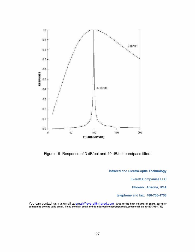
The combination of the two than make a band pass filter with 3 dB/oct roll-off at both the high and low frequency ends. This is good, but it is hardly ever sufficient. One can use active RC and switched capacitor filter integrated circuits to good effect. It is not at all difficult to get 40-120 dB/oct roll-offs and higher. Figure 16 illustrates the noise rejection properties one can get this way. The 120 dB/oct curve is not shown since it would appear as just a spike or vertical line at 100 Hz on this scale. In this example, 100 Hz is the modulation frequency and the radiation generated signal appears in a very narrow band at 100 Hz. If we assume that we are well above the 1/f knee, the noise is spread uniformly over the frequency spectrum. The noise contribution to the output signal is proportional to the area under the passband curve. It is clear that the signal-to-noise ratio with a 40 dB/oct passband is going to be very much larger than it would be with a 3 dB/oct passband. The high and low corner frequencies in Figure 16 have both been set to the same frequency, 100 Hz. The high and low corner frequencies can be set to different values creating a pass band with fairly flat response between the two corner frequencies and sharp fall-off on either side. Doing this allows for drift in the modulation frequency or tracking of a changing input signal. Of course, it also lets more noise through thereby reducing the signal-to-noise ratio
If the incident radiation is modulated, the analog output signal will be at the modulation frequency or one of its harmonics. If this signal is then passed to the digital domain, the ADC must be fast enough to deal with it, as mentioned above, or something like an rms-to-dc converter must be used. These converters are available as integrated circuits and are quite effective except one has to be careful to properly low pass filter the output. Both approaches works, and the choice really depends on the application.
27
Figure 16 Response of 3 dB/oct and 40 dB/oct bandpass filters
Infrared and Electro-optic Technology
Everett Companies LLC
Phoenix, Arizona, USA
telephone and fax: 480-706-4753
You can contact us via email at [email protected] (Due to the high volume of spam, our filter sometimes deletes valid email. If you send an email and do not receive a prompt reply, please call us at 480-706-4753)