practical manual lab: dsd - rps group of institutions manual/dsdlab… · · 2015-03-27practical...
TRANSCRIPT

Practical Manual
Lab: DSD (EE-330-E)
EXPERIMENT 1
Aim:- Write the VHDL CODE & SIMULATE IT FOR THE FOLLOWING GATES.
i) Two i/p And Gates. ii) Two i/p OR Gates.
iii) Two i/p NAND Gates iv) Two i/p Nor Gates.
v) Two i/p Ex-OR Gates. vi) NOT Gates.
Electronics &Communication Engg. (ECE)
RAO PAHALD SINGH GROUP OF INSTITUTIONS
BALANA(MOHINDER GARH)123029
Prepared By. Checked By.
Mr.SANDEEP KUMAR Mr.PAWAN KUMAR

Cad Tool Required:- Mentor Graphics FPGA Advantage Software Modelsim Simulation
Tool.
Program:- i) Behavior Model if two i/p And Gates.
Library IEEE;
Use IEEE.std_logic_1164.all; Use IEEE.std_logic_arith.all;
Entity and2 is
Port (a, b: in bit; z: out bit); End and2;
Architecture beh of and2 is Begin process (a, b)
Begin If (a=’0’ and b=’0’) then
Z<=’0’; ElsIf (a=’0’ and b=’1’) then
Z<=’0’; ElsIf (a=’1’ and b=’0’) then
Z<=’0’; ElsIf (a=’1’ and b=’1’) then
Z<=’1’; End if;
End process; End beh;
CKT Diagram:-
1
2
3
A
B Z
AND_2 TRUTH TABLE
a b Z
0 0 0
0 1 0
1 0 0
1 1 1
Logic Equation: Z=a.b

ii) Behavior Model if two i/p OR Gates
Library IEEE; Use IEEE.std_logic_1164.all;
Use IEEE.std_logic_arith.all;
Entity OR_2 is Port (a, b: in bit; z: out bit);
End OR_2;
Architecture OR_2_beh of OR_2 is Begin process (a,b)
Begin If (a=’0’ and b=’0’) then
Z<=’0’; Elsif (a=’0’ and b=’1’) then Z<=’1’; Elsif (a=’1’ and b=’0’) then Z<=’1’; Elsif (a=’1’ and b=’1’) then Z<=’1’; End if; End process;
End OR_2_beh;
CKT Diagram:-
1
2
3
ZA
B
OR_2 TRUTH TABLE
a b Z
0 0 0
0 1 1
1 0 1
1 1 1
Logic Equation: Z=a+b

iii) Behavior Model if two i/p NAND Gates
Library IEEE; Use IEEE.std_logic_1164.all;
Use IEEE.std_logic_arith.all;
Entity NAND_2 is Port (a, b: in bit; z: out bit);
End NAND_2;
Architecture NAND_2_beh of NAND_2 is
Begin process (a, b) Begin
If (a=’0’ and b=’0’) then Z<=’1’; Elsif (a=’0’ and b=’1’) then Z<=’1’; Elsif (a=’1’ and b=’0’) then Z<=’1’; Elsif (a=’1’ and b=’1’) then Z<=’0’; End if; End process;
End NAND_2_beh;
CKT Diagram:-
ZA
B
1
2
3
NAND_2 TRUTH TABLE
a b Z
0 0 1
0 1 1
1 0 1
1 1 0
Logic Equation: Z=a.b

iv) Behavior Model if two i/p NOR Gates
Library IEEE;
Use IEEE.std_logic_1164.all; Use IEEE.std_logic_arith.all;
Entity NOR_2 is
Port (a, b: in bit; z: out bit);
End NOR_2;
Architecture NOR_2_beh of NOR_2 is Begin process (a, b)
Begin If (a=’0’ and b=’0’) then
Z<=’1’; Elsif (a=’0’ and b=’1’) then
Z<=’0’; Elsif (a=’1’ and b=’0’) then
Z<=’0’; Elsif (a=’1’ and b=’1’) then
Z<=’0’; End if;
End process;
End NOR_2_beh;
CKT Diagram:-
1
2
3
A
BZ
NOR_2 TRUTH TABLE
a b Z
0 0 1
0 1 0
1 0 0
1 1 0
Logic Equation: Z=a+b

(iv)Behavior Model if two i/p EX-OR Gates
Library IEEE; Use IEEE.std_logic_1164_all;
Use IEEE.std_logic_arith_all;
Entity EXOR_2 is Port (a, b: in bit; z: out bit);
End EX-OR_2;
Architecture EXOR_2_beh of EXOR_2 is
Begin Process (a, b)
Begin If (a=’0’ and b=’0’) then
Z<=’0’; Elsif (a=’0’ and b=’1’) then
Z<=’1’; Elsif (a=’1’ and b=’0’) then
Z<=’1’; Elsif (a=’1’ and b=’1’) then
Z<=’0’; End if;
End process; End EXOR_2_beh;
CKT Diagram:-
A
BZ
1
2
3
EX-OR_2 TRUTH TABLE
a b Z
0 0 0
0 1 1
1 0 1
1 1 0
Logic Equation: Z=

v) Behavior Model of NOT Gate
Library IEEE; Use IEEE.std_logic_1164_all;
Use IEEE.std_logic_arith_all;
Entity NOT_2 is Port (a: in bit; z: out bit);
End NOT_2;
Architecture EXOR_2_beh of EXOR_2 is
Begin Process (a)
Begin If (a=’0’) then
Z<=’1’; Elsif (a=’1’) then
Z<=’0’; End if;
End process; End NOT_2_beh;
CKT Diagram:-
1 2
A Z
NOT_2
Precautions:- Make sure that there is no syntax and semantie error.
Result:- All the VHDL codes of AND, OR, NAND, NOR, EX-OR and NOT gates are
simulated & find correct

Practical Manual
Lab: DSD
(EE-330-E)
EXPERIMENT NO.-2
Aim:-
Write behavior model of 1- bit Comparator.
Electronics &Communication Engg. (ECE)
RAO PAHALD SINGH GROUP OF INSTITUTIONS
BALANA(MOHINDER GARH)123029

Cad Tool Required:- Mentor Graphics FPGA Advantage Software Modelsim Simulation Tool.
Program:-
Library IEEE;
Use IEEE.std_logic_1164.all; Use IEEE.std_logic_arith.all;
Entity CMP_2 is Port (a, b: in bit; ALB, AGB, AEB: out bit);
End CMP_2;
Architecture CMP_2_beh of CMP_2 is Begin
Process (a, b) Begin
If (a=’0’ and b=’0’) then ALB<=’0’; AGB<=’0’; AFB<=’1’; Elsif (a=’0’ and b=’1’) then ALB<=’1’; AGB<=’0’; AFB<=’0’; Elsif (a=’1’ and b=’0’) then
ALB<=’0’; AGB<=’1’; AFB<=’0’; Elsif (a=’1’ and b=’1’) then
ALB<=’0’; AGB<=’0’; AFB<=’1’; End if;
End process; End CMP_2_beh;

Block Diagram:-
A A>B
A=B
B A<B
Precautions:-
Make sure that there is no syntax and semantie error.
Result:-
All the VHDL codes of 1- bit Comparator is simulated & synthesized.
1- Bit
Comparator

Practical Manual
Lab:DSD. (EE-330-E)
EXPERIMENT NO.-3
Aim:-
Write a program for behavior model of 4- bit
Comparator
Electronics &Communication Engg. (ECE)
RAO PAHALD SINGH GROUP OF INSTITUTIONS
BALANA(MOHINDER GARH)123029

Cad Tool Required:- Mentor Graphics FPGA Advantage Software Modelsim Simulation Tool.
Program:-
Library IEEE; Use IEEE.std_logic_1164.all;
Use IEEE.std_logic_arith.all;
Entity COM_2 is
Port (a, b: in bit_Vector (3 down to 0); z: out bit_vector (2 down to 0)); End COM_2;
Architecture COM_2_beh of COM_2 is
Begin Process (a, b)
Begin If (a=b) then
Z<=’100’; Elsif (a<b) then
Z<=’010’; Elsif (a>b) then
Z<=’001’; End if; End process;
End COM_2_beh;
Precautions:-
Make sure that there is no syntax and semantie error.
Result:- All the VHDL codes of 4- bit Comparator is simulated & synthesized.

Practical Manual
Lab: DSD
(EE-330-E)
EXPERIMENT NO.-4
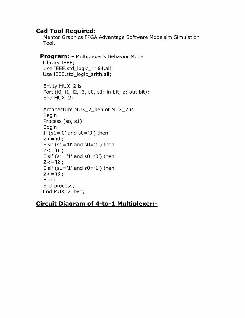
Aim:- Write the VHDL CODE & SIMULATE IT FOR 4:1 MUX &
4:1 Demultiplexer.
Electronics &Communication Engg. (ECE)
RAO PAHALD SINGH GROUP OF INSTITUTIONS
BALANA(MOHINDER GARH)123029
Cad Tool Required:- Mentor Graphics FPGA Advantage Software Modelsim Simulation Tool.
Program: - Multiplexer’s Behavior Model Library IEEE;
Use IEEE.std_logic_1164.all;
Use IEEE.std_logic_arith.all;
Entity MUX_2 is Port (i0, i1, i2, i3, s0, s1: in bit; z: out bit);
End MUX_2;
Architecture MUX_2_beh of MUX_2 is Begin
Process (so, s1) Begin
If (s1=’0’ and s0=’0’) then
Z<=’i0’; Elsif (s1=’0’ and s0=’1’) then
Z<=’i1’; Elsif (s1=’1’ and s0=’0’) then
Z<=’i2’; Elsif (s1=’1’ and s0=’1’) then
Z<=’i3’; End if;
End process; End MUX_2_beh;
Circuit Diagram of 4-to-1 Multiplexer:-

Select Input’s
S1 S0
Output
Y
0 0 I0
0 1 I1
1 0 I2
1 1 I3
Truth table of 4-to-1 Multiplexer Program: - Behavior Model of Demultiplexer (1 to 4)
Library IEEE;
Use IEEE.std_logic_1164_all; Use IEEE.std_logic_arith_all;
Entity DEMUX_2 is
Port (a, s0, s1: in bit; z: out bit_vector (3 down to 0)); End DEMUX_2;
Architecture DEMUX_2_beh of DEMUX_2 is
Begin Process (so, s1)
Begin
If (s1=’0’ and s0=’0’) then Z (0) <=a;
Z (1) <=’0’; Z (2) <=’0’; Z (3) <=’0’; Elsif (s1=’0’ and s0=’1’) then
Z (0) <=’0’; Z (1) <=a;
Z (2) <=’0’; Z (3) <=’0’; Elsif (s1=’1’ and s0=’0’) then Z (0) <=’0’;
A0
A1
A2
A3
I1 I0
O0
10
11
12
13
U
V
W
X
S0 S1
S0 BAR S1 BAR

Z (1) <=’0’; Z (2) <=a; Z (3) <=’0’; Elsif (s1=’1’ and s0=’1’) then Z (0) <=’0’; Z (1) <=’0’; Z (2) <=’0’; Z (3) <=a; End if;
End process; End DEMUX_2_beh;
Precautions:-
Make sure that there is no syntax and semantic error.
Result:- A) All the VHDL codes of 4 to 1 Multiplexer is simulated & synthesized.
B) All the VHDL codes of 4 to 1 Demultiplexer is simulated & synthesized.

Practical Manual
Lab: DSD (EE-330-E)
EXPERIMENT NO.-5
Aim:-
Write a program for behavior model of BCD to
Seven Segment Decoder.
Electronics &Communication Engg. (ECE)
RAO PAHALD SINGH GROUP OF INSTITUTIONS
BALANA(MOHINDER GARH)123029

Cad Tool Required:- Mentor Graphics FPGA Advantage Software Modelsim Simulation Tool.
Program:-
Library IEEE; Use IEEE.std_logic_1164.all;
Use IEEE.std_logic_arith.all;
Entity BCD_2 is
Port (b: in bit_Vector (3 down to 0); z: out bit_vector (6 down to 0)); End BCD_2;
Architecture BCD_2_beh of BCD_2 is
Begin Process (b)
Begin Case B is
When “0000”=> S<=”1111110”; When “0001”=> S<=”0110000”; When “0010’=> S <=”1101101”; When “0011”=>
S<=”1111001”; When “0110”=>
S<=”1011111”; When”0111”=>
S<=”1110000”; When”1000”=>
S<=”1111111”; When”1001”=>
S<=”1110011”; When other =>
S<=”000000”; End case;
End process; End BCD_Beh;

Block Diagram of BCD-to-Seven Segment Decoder
BCD Input’s
A B C D
Output’s
a b c d e f g
0 0 0 0 1 1 1 1 1 1 0
0 0 0 1 0 1 1 0 0 0 0
0 0 1 0 1 1 0 1 1 0 1
0 0 1 1 1 1 1 1 0 0 1
0 1 0 0 0 1 1 0 0 1 1
0 1 0 1 1 0 1 1 0 1 1
0 1 1 0 1 0 1 1 1 1 0
0 1 1 1 1 1 1 0 0 0 0
1 0 0 0 1 1 1 1 1 1 1
1 0 0 1 1 1 1 1 0 1 1
Truth table of BCD-to-Seven Segment Decoder
BCD-to-Seven
Segment Decoder
A
B
C
D
a
b
c
d
e
f
g
g
a
d
f
e
b
c

Wave Form of BCD-to-Seven Segment Decoder:-
Precautions:-
Make sure that there is no syntax and semantie error.
Result:- All the VHDL codes of BCD to Seven Segment is simulated &
synthesized.

Practical Manual
Lab: DSD
(EE-330-E)
EXPERIMENT NO.-6
Aim:-
Write a VHDL program for behavior model of
PIPO.
Electronics &Communication Engg. (ECE)
RAO PAHALD SINGH GROUP OF INSTITUTIONS
BALANA(MOHINDER GARH)123029

Cad Tool Required:- Mentor Graphics FPGA Advantage Software Modelsim Simulation Tool.
Program:- Library IEEE;
Use IEEE.std_logic_1164.all; Use IEEE.std_logic_arith.all;
Entity PIPO_2 is Port (Pr, Cr, Clk: in bit; D: is bit_vector (2 down to 0); Q: out
bit_vector (2 down to 0)); End PIPO_2;
Architecture PIPO_2_beh of PIPO_2 is
Begin Process (Pr, Cr, Clk, D)
Begin If (Pr=’0’ and Cr=’1’) then
Q<=’111’; Elsif (Pr=’1’ and Cr=’0’) then
Q<=’000’; Elsif (Pr=’0’ and Cr=’1’) then
Q<=’0’; Elsif (Pr=’1’ and Cr=’1’) then Q<=’111’; Elsif (Pr=’1’ and Cr=’1’and Clk=’0’ and Clk’s event) then Q<=’D;
End if; End process;
End PIPO_2_beh;

Block diagram of 4-bit Parallel in Parallel out Register
Waveform of 4-bit Parallel in Parallel Out Register:-
D Q
FF0
D Q
FF1
D Q
FF2
D Q
FF3
D(0) D(1) D(2) D(3)
PR
CLK
CR
Parallel Input's
Parallel Output's

Precautions:-
Make sure that there is no syntax and semantie error. Result:-
All the VHDL codes of PIPO is simulated & synthesized.
Practical Manual
Lab: DSD (EE-330-E)
EXPERIMENT NO.-7
Aim:-
Write VHDL programs for the following ckt, check
the wave forms and hardware generated.
A. Half Adder.
B. Full Adder.
Electronics &Communication Engg. (ECE)
RAO PAHALD SINGH GROUP OF INSTITUTIONS
BALANA(MOHINDER GARH)123029

Cad Tool Required:- Mentor Graphics FPGA Advantage Software Modelsim Simulation Tool.
Program: -
A). Behavior Model of Half Adder:- Library IEEE;
Use ieee.std_logic_1164.all; Use ieee.std_logic_arith.all;
Entity HA_2 is
Port (a, b: in bit; s, c: out bit); End HA_2;
Architecture HA_2_beh of HA_2 is Begin
Process (a, b) Begin
If (a=’0’ and b=’0’) then S<=’0’; C<=’0’; Elsif (a=’0’ and b=’1’) then S<=’1’; C<=’0’; Elsif (a=’1’ and b=’0’) then
S<=’1’; C<=’0’; Elsif (a=’1’ and b=’1’) then S<=’0’; C<=’1’; End if;
End process; End HA_2_beh;

B) Behavior Model of FULL Adder:-
Library IEEE;
Use ieee.std_logic_1164.all; Use ieee.std_logic_arith.all;
Entity FA_2 is Port (a, b, cin: in bit; s, c: out bit);
End FA_2;
Architecture FA_2_beh of FA_2 is Begin
Process (a, b,cin) Begin
S<=a XOR B XOR Cin; C<= (a and b) OR (a and cin) OR (b and cin);
End process; End FA_2_beh;
Circuit Diagram of Full Adder
Input’s
A B Cin
Output’s
S C
0 0 0 0 0
0 0 1 1 0
0 1 0 1 0
0 1 1 0 1
1 0 0 1 0
1 0 1 0 1
1 1 0 0 1
O0
A1
A2
A0
X0
A
B
Cin
S
C

1 1 1 1 1
Truth table of Full Adder
Wave Form:-
Precautions:-
Make sure that there is no syntax and semantic error.
Result:-
A) All the VHDL codes of Half Adder is simulated & synthesized. B) All the VHDL codes of Full Adder is simulated & synthesized.
.
Practical Manual
Lab: DSD (EE-330-E)
EXPERIMENT NO.-8
Aim:-
Write VHDL programs for ALU.
Electronics &Communication Engg. (ECE)
RAO PAHALD SINGH GROUP OF INSTITUTIONS
BALANA(MOHINDER GARH)123029

Cad Tool Required:- Mentor Graphics FPGA Advantage Software Modelsim Simulation Tool.
Program: -
Behavior Model of ALU.
Library IEEE;
Use ieee.std_logic_1164.all; Use ieee.std_logic_arith.all;
Entity ALU_2 is
Port (p, q: in bit_vector (3 down to 0); s: in bit_vector (2 down to 0); f: in bit_vector (3 down to 0));
End ALU_2;
Architecture ALU_2_beh of ALU_2 is Function of “+” Function add (a, b: bit_vector (2 down to 0) Return bit_vector is
Variable cout: bit; Variable cin: bit;
Variable sum: bit_vector (2 down to 0); Begin
For i: in 0 to 2 loop Sum (i): a (i) XOR b (i) XOR Cin;
Cout: = (a (i) and b (i)) OR (b (i) and Cin) OR (Cin And a (i)); Cin: = Cout
End loop; Return sum;
End “+” --function of subtraction of 2 bit array Function “-“(a, b: bit_vector (3 down to 0
Return bit_vector is Variable cout: bit;
Variable Cin: bit=’0’; Variable diff (i): bit_vector (3 down to 0);
Begin For I in 0 to 3 loop
Cout: = ((not a (i) and b (i)) or ((b (i) and cin) or ((not a (i) and cin)) ; Diff (i):= a (i) xor b (i) xor cin;
Cin: = cout; End loop;
Return diff (i); End “-“;
Begin Process (p, q, and s)
Begin Case s is
When “000”=>

F<= “0000”; When “001” => F =q-p;
When “010”=> F =p-q;
When “001”=> F =p+q;
When “100”=> F =p and q;
When “101”=> F<= p xor q;
When “110”=> F<=p or q:
When “111” => F<= “1111”; End case;
End process; End ALU_Beh;
Circuit Diagram of ALU
P(3)
P(2)
P(1)
P(0)
ALU
74381 Q(3)
Q(2)
Q(1)
Q(0)
S2 S1 S0
Q Input
(4-bit)
F(3)
F(2)
F(1)
F(0)
F Output
(4-bit)
Select Line (4 bit)
P Input
(4-bit)

Select Input
S2 S1 S0
Operation Output
F
0 0 0 CLEAR 0 0 0 0
0 0 1 Q – P Q – P
0 1 0 P – Q P – Q
0 1 1 ADD P + Q
1 0 0 XOR P XOR Q
1 0 1 OR P OR Q
1 1 0 AND P AND Q
1 1 1 PRESET 1 1 1 1
Function Table of ALU(74381)
Waveform of ALU:-
Precautions:-
Make sure that there is no syntax and semantic error.
Result:- All the VHDL codes of ALU is simulated & synthesized.

Practical Manual
Lab: DSD (EE-330-E)
EXPERIMENT NO.-9
Aim:-
Write a VHDL program for behavior model of D
Flip - Flop.
Electronics &Communication Engg. (ECE)
RAO PAHALD SINGH GROUP OF INSTITUTIONS
BALANA(MOHINDER GARH)123029

Cad Tool Required:-
Mentor Graphics FPGA Advantage Software Modelsim Simulation
Tool.
Program:-
Library IEEE;
Use IEEE.std_logic_1164.all; Use IEEE.std_logic_arith.all;
Entity DIFF_2 is
Port (Pr, Cr, Clk: in bit; D: is bit_vector (2 down to 0); Q: out
bit_vector (2 down to 0)); End DIFF_2;
Architecture DIFF_2_beh of DIFF_2 is
Begin Process (Pr, Cr, Clk, D)
Begin If (Pr=’0’ and Cr=’1’) then
Q<=’1’; Elsif (Pr=’1’ and Cr=’0’) then
Q<=’0’; Elsif (Pr=’1’ and Cr=’1’and Clk=’0’ and Clk’s event) then
Q<=D;
End if;
End process; End DIFF_2_beh;

Block Diagram of D- Flip FloP
PR CR D(i/p) Output
Q(t + 1)
0 0 X 1
0 1 X 1
1 0 X 0
1 1 0 0
1 1 1 1
Truth table of D flip-flop
D Q
FF
Input
Clk
PR
Q
CR

Waveforms of D flip flop:-
Precautions:-
Make sure that there is no syntax and semantic error.
Result:-
All the VHDL codes of D-Flip-Flop is simulated & synthesized.

Practical Manual
Lab: DSD (EE-330-E)
EXPERIMENT NO.-10
Aim:-
Write a VHDL program for behavior model of 3-
Bit UP Counter.
Electronics &Communication Engg. (ECE)
RAO PAHALD SINGH GROUP OF INSTITUTIONS
BALANA(MOHINDER GARH)123029

Cad Tool Required:- Mentor Graphics FPGA Advantage Software Modelsim Simulation Tool.
Program:-
Library IEEE;
Use IEEE.std_logic_1164.all; Use IEEE.std_logic_arith.all;
Entity COUNTER_2 is Port (Pr, Cr, Clk, t: in bit; Q: out bit_vector (0 to 2));
End DIFF_2;
Architecture COUNTER _2_beh of COUNTER _2 is Function of “+” Function add (a, b: bit_vector (0 down to 2)) Return bit_vector is
Variable cout: bit; Variable cin: bit: = ‘0’; Variable sum: bit_vector (0 to 2):= “000”; Begin
For i: in 0 to 2 loop Cout: = (a (i) and b (i)) OR (b (i) and Cin) OR (Cin And a (i));
Sum (i): a (i) XOR b (i) XOR Cin;
Cin: = Cout End loop;
Return sum; End “+”; Begin Process (Clk, Pr, Cr)
Begin If (Pr=’0’ and Cr=’1’) then
Q<= ‘111’; Elsif (Pr=’1’ and Cr=’0’) then
Q<= ‘000’; Elsif (Pr=’1’ and Cr=’1’and Clk=’0’ and Clk’s event) then
Q<=Q+ “000”;
End if;
End process; End COUNTER _2_beh

Block Diagram of 3-bit UP Counter
Waveform of 3-bit Up Counter:-
Precautions:-
Make sure that there is no syntax and semantic error.
Result: - All the VHDL codes of D-Flip-Flop is simulated &
synthesized.
T Q
FF0
T Q
FF1
T Q
FF2
T
PR
CLK
CR
Q (0) Q(1) Q(2)
LSB Parallel Output’s MSB