power system applications of fiber optic sensors · jpl publication 86-22 doetet 29372-5...
TRANSCRIPT

JPL Publication 86-22 DOEtET 29372-5
Distribution Category UC-97b
Power System Applicationsof Fiber Optic Sensors
A. R. JohnstonS. P. Jackson
H. Kirkham
C. Yeh
June 1986
Prepared for
Office of Energy Storage and DistributionU.S. Department of Energy
Through an Agreement withNational Aeronautics and Space Administration
by
Jet Propulsion LaboratoryCalifornia Institute of TechnologyPasadena, California
https://ntrs.nasa.gov/search.jsp?R=19870002904 2018-06-17T07:25:14+00:00Z

Prepared by the Jet Propulsion Laboratory, California Institute of Technology,
for the U.S. Department of Energy through an agreement with the National
Aeronautics and Space Administration.
This report was prepared as an account of work sponsored by an agency of the
United States Government. Neither the United States Government nor any
agency thereof, nor any of their employees, makes any warranty, express or
implied, or assumes any legal liability or responsibility for the accuracy, com-
pleteness, or usefulness of any information, apparatus, product, or process
disclosed, or represents thai its use would not infringe privately owned rights.
Reference herein to any specific commercial product, process, or service by trade
name, trademark, manufacturer, or otherwise, does not necessarily constitute or
imply its endorsement, recommendation, or favoring by the United States
Government or any agency thereof. The views and opinions of authors
expressed herein do not necessarily slate or reflect those of the United States
Government or any agency thereof.
This publication reports on work performed under NASA Task RE-152, Amend-
ment 203 and sponsored through DOE/NASA Interagency Agreement No.
DE-AI01-79ET 29372 (Mod. AO09).

_S_A_
This document is a progress report of work done in 1985 on the Communications
and Control for Electric Power Systems Project at the 3et Propulsion
Laboratory. Three topics are covered: Electric Field Measurement, Fiber Optic
Temperature Sensing, and Optical Power Transfe_
Work was done on the measurement of ac and dc electric fields. A prototype
sensor for measuring alternating flelds was made using a very slmple
electroscope approac_ An electronic field mill sensor for dc fields was made
using a fiber optic readout, so that the entire probe could be operated
isolated from 8roun&
_he=e are several instances in which more precise knowledge of the temperature
of electrical power apparatus would be useful This report describes a number
of methods whereby the distributed temperature profile can be obtained using a
fiber optic senso_
The ability to energize electronics by means of an optical fiber has the
advantage that electrical isolation is maintained at low cost In order to
accomplish this, it is necessary to convert the light energy into electrical
form by means of photovoltaic cells. JPL has developed an array of PV cells
in gallium arsenide specifically for this purpose. This work is describe&
iii

ACKNOWLEI_MENTS
_xe research described in this report was carried out at the Jet P_opulsion
Laboratory (JPL), California Institute of Technology, and was sponsored by the
U.S. Department of Energy, Office of Energy Storage and Distribution, through an
agreement with NASA.
The authors thank Ken Klein of DOE's Office of Energy Storage and Distribution
for his continued help and encouragement_ We also thank Luclano Zafanella and
the staff of General Electric's High Voltage Transmission Research Facility for
their time and assistance. In particular, we thank Gary _ohnson and Bill
McGonigle for their assistance in preparing for and conducting the tests at the
High Voltage Transmission Research Facility. We also acknowledge the
contribution of Bjorn Eng at _FL in the design and construction of the prototypedc field sensor, as well as the help of Keith Sheu (also at JPL) in assembllng
the electronlcs.
E
!s!
iv

TABLE OF CONTENTS
Xe Introduction .......................... 1-1
1.1 Power System Sensors ................... l-1
0 Electric Field Measurement ................... 2-1
2.1 Introduction ....................... 2-1
2.2 AC Field Measurement ................... 2-3
2.3 DC Field Measurement ................... 2-9
2.3.1 Theoretical Background ............... 2-9
2.3.2 Sensor Design ................... 2-152.3.3 Position-Reference Encoding ............ 2-18
2.3.4 The Optical Link .................. 2-18
2.3.5 Laboratory l_valuation ............... 2-182.3.6 Field Tests .................... 2-23
2.3.7 Self-Charging Experhnents ............. 2-31
2.3.7.1 Experimental Test Arrangement ....... 2-312.3.7.2 Paraueter Measurements .......... 2-33
2.3.8 Conclusions .................... 2-39
. Fiber Optic Temperature Sensing ................ 3-1
3.1 Applications ....................... 3-1
3.1.1 Overhead Phase Conductor Temperature Measurement . . 3-1
3.1.2 Underground Cable Temperature Measurement ..... 3-2
3.1.3 Power System Equipment Temperature Monitoring . . . 3-2
3.2 Methods of Measuring Temperature Distribution ....... 3-3
3.2.1 Temperature Dependent Birefringence ........ 3-5
3.2.2 Temperature Dependent Loss ............. 3-53.2.3 Coupling Variations with Temperature ........ 3-7
3.2.4 Temperature Dependent Optical Index Ratio ..... 3-7
3.2.5 Temperature Dependence of Refractive Index ..... 3-11
3.2.6 Point Sensing for Distributed Measurement ..... 3-11
3.2.7 Distance Reached by a Lossy Distributed Sensor . . . 3-14
. Optical Power Transfer ..................... 4-1
4.1 Background ........................ 4-1
4.2 Device Design Parameters ................. 4-5
4.2.1 ]he GaAs starting wafers .............. 4-5
4.2.2 Light Capture Area and Conversion Efficiencies . . . 4-74.2.3 Device Fabrication ................. 4-14
4.2.4 Teat Results .................... 4-16
4.3 Future Work ........................ 4-16
5, Conclusions .......................... 5-1
REFI_qCES ................................ 6-1
V

FIGURES
2-1 Examples of Field Mill Designs 2-2
2-2 Laboratory Model of Fused Silicon Fiber Electroscope withMetallized Fiber 2-4
2-3 Photograph of the Fiber Electroscope as Built ............ 2-6
2-4 Input-Output Curve for an All-Dielectric Test Model of the Fiber
Elec troscope . 2-7
2-5 An All-Dielectrlc Configuration of the Fiber Electroscope Sensor . . 2-8
2-6 Geometry of Split-Cylinder Sensor Probe ............... 2-10
2-7 Fractional Change in Sensor Output Induced by a Nearby Conducting
Surface for Full Ion Current Charging ................ 2-14
2-8 Photograph of the Prototype Sensor with One-Half Cylindrical ShellRemoved to Show Internal Parts 2-16
2-9 Functional Block Diagram of the Sensor Electronics ......... 2-17
2-10a Schematic of DC Field Sensor Probe ................. 2-19
2-10b Schematic of DC Field Sensor Receiver ............... 2-20
2-11 Typlcal AC Output as Seen at the Receiver .............. 2-21
2-12 Output of Sensor at Rotational Frequencies Corresponding to Speeds
between 600 and 4200 rvn ..................... 2-22
2-13 Calibration Curve Obtained in BVTRF Test Cage ............ 2-24
2-14 Electric Field Vectors Measured Near a Test Subject ......... 2-26
2-15 Measurement of Electric Field in the Vicinity of a Person ...... 2-27
2-16 Electric Field Versus Time Measured Under DC Conductor, Ccmpared to
IIVTRF Data 2-29• • • • • • • • e • • • • • • • • • • • • • • • • • • • •
2-17 Measured Field Values Along s Line Crossing Pemanent
Instrumentation 0.6 m Above Ground .................. 2-30
2-18 Field Cage and Test Bench Arrangement ................ 2-32
2-19 Measured Sensor Output as a Function of Electric Field ....... 2-34
2-20 Example ShowingArrangement Used to Produce an Excess Voltageof +1027 V on the Sensor ...................... 2-35
vi

2-21 SensorOutputvs. SensorExcessVoltage fo_ Various Ratios ofd to r. E Field Constant at 30 kV/m ................ 2-36
2-22 I_asured Change in Sensor Output as a Function of Distance to
Screen, Sensor Uncharsed ...................... 2-37
2-23 Measured Change in Sensor Output as a Function of Distance to
Screen Sensor Fully Charsed (-2.64 kV) ............... 2-38
3-1 Optical Time Domain Reflectometrya) Optical Time-domain Reflectometer ............... 3-4
b) OTDR display .......................... 3-4
3-2 Birefringence Sensins ........................ 3-6
3-3 Temperature-Dependent J/icrobending Loss ............... 3-8
3 4 Tes_rature-i)ependent Couplinl 3-9
3-5 Temperature-Dependent Optical Index Ratio .............. 3-10
3-6 Temperature-Dependent Refractive Index ............... 3-12
3-7 s. Separate Sensors Using Optical Fiber as Communication Channel.. 3-13b. Separate Sensors Spaced Within the Resolution of the (YIDR . . . 3-13
4-1 Block Diasram of Optical Power Transfer System ........... 4-2
4-2 Electrical and Physical Arrangenent of 32-Diode Array ........ 4-3
4-3 Sequence of Rvents in Producing Gallium Arsenide Diode Array .... 4-4
4-4 Diode Array Layout and Mounting Arrangements ............ 4-6
4-5 Gallinu Arsentde Wafer Dicing, showing Sawed l_lge .......... 4-8
4-6 Two Views of a Laser-Scribed Gallium Arsenide Wafer ......... 4-9
4-7 Edge of Galli nm Arsenide Wafer Scribed Sider-to-Side ......... 4-10
4-8 Two Views of a Diamond-scribed Gallium Arsenide Wafer ........ 4-11
4-9 Two Views of a Gallinm Arsenide Wafer Cut with a Diamond Saw .... 4-12
4-10 Photodiode Array Mounting Arrangement on Fiber Connector ...... 4-13
4-11 Photograph of 32-Diode Array .................... 4-15
vii

i
E
m_
_F
t
_E
|
i
iL
E
mE
Z

SECTION 1
INTRODUCTION
The word optic comes from the greek o?r_Ko_, meaning eye. As a noun the word
has traditionally been applied to any element of an optical system, but in
particular it has been the collective noun for items such as lenses andmirrors.
One thing that such optics had in common was that they were much wider than
their lengt_ Uncounted numbers of independent rays of light can be made to
pass through a small lens, for example, and a mirror reflects any lightimpinging upon it, regardless of the direction the light is coming from. This
feature of optics, the aspect rati_ changed in the 1970s, and particularly in
the 1980s, with the advent of fiber optics, optical components whose lengthsare millions of times their width. In these components, the light can only be
inserted into the optical element from near the axis of the fiber. Once it is
coupled into the optic, light emerges from the other end almost unaltered by
physical interactions between the fiber and the medium through which itpasses. Modulated_light (or light which is switched on and off rapidly) can
be made to pass through considerable lengths of fiber without degradation.
This fact made optical fibers'extremely attractive in the telecommunications
industry, which has been quick to demonstrate the superiority of opticalfibers as transmitters of information.
Not only are optical fibers immune to their physical and chemical environment,they are also relatively immune to the electromagnetic envtronmenL Thisfeature makes them of considerable interest in the electric power industry.
Since 1983, The Communications and Control for Electric Power Systems Task at
the 3et Propulsion Laboratory (JPL), funded by the Department of Energy (DOE),
has been investigating the application of optical fibers to power systems. A
good deal of that effort has been aimed at using fiber optics as sensors in
power systems.
This report is a summary of the work done at JPL in this area over the last
twelve months.
1.1 POWER SYSTEM S_NSORS
Klectrtc power systems comprise some of the largest and most complicated
systems in the world: They are widespread both geographically andhierarchically, that is to say they cover large areas of land and tnclnde
wlth/n a given area elements of generation, transmission and distribution.
They are wldely interconnected and contain, from an analysls point of view,
large numbers of nodes. The calculation of the state of an entire power
system at any glee instant is a formldable task, which even today requires
several seconds of computer time on the very largest and fastest computers,
The calculations begin with measured data. In the case of a typical power
system, data on many hundreds or even thousands of parameters will be
collected by the Supervisory Control and Data Acquisition (SCADA) system and
1-1

relayed back to the energy control center. _he measured data will typically
include voltage and current at a large number of buses in the transmission
system, a smaller number in the subtransmission system, and perhaps some ofthe distribution system parameters, as well as data concerning the status of
the generators in the system. (One might note in passing that the unknown in
the equation which describes the power system state is the load on the power
system. )
_he fact that there are so many sensed values in a power system has led to aconsiderable amount of interest in the development of low cost sensors based
on fiber optics. Several companies, particularly in 3apan, have been active
in developing sensors for the primary electrical quantities (voltage and
current) for ranges which are realistic in power systems, thousands of volts
and thousands of crops.
:=
:!
At the time of this writing, fiber optic power system sensors have developedto a point where they are competitive with some of the conventional
approaches, using, for example, voltage transformers and current transformers.However, they have not yet shown themselves to have a clear performance or
economic advantage. _'nis will change, nonetheless, since magnetic and
capacitive sensors have been developed over many decades to a point of
considerable refinement, whereas the optical techniques are just beginning to
be develope&
1_ne decision was made early on in the fiber optic sensors work of theCommunications and Control Task at 3PL to concentrate on developing a new
measurement technique, rather than the refinement of a method of whose
practicality had already been shown Be measurement of electric fields inair was chosen for the initial sensor efforts.
While the electric fields caused by power lines can be measured in the plane
of the ground, their measurement outside of that plane is difficult. _he
development of a suitable sensor to accomplish this measurement has provided
some interesting challenges.
Sensors for measuring alternating electric fields outside the ground plane had
previously been demonstrated. These instruments consisted of a current
measuring device placed between the electrodes of a large capacitor, measuring
the displacement current between the electrodes, in such a way that the
investigator could read the instrument when it was held a meter or two from
him at the end of a fiberglass pole. There was typlcally no way to record
the intensity of the electric field other than for the investigator to note
the reading of the instrument.
A fairly simple modification of this principle would be to encode the datainto optical form and insert it into an optical fiber which runs along the
fiberglass pole. In this way the information can be read from the instrument
by a data acquisition system without perturbing the electric field any more
than it already is.
1-2
m
=
|
.!i
_=

The measurement of direct electric fields can, in principle, be done the same
way provided that the capacitor electrodes rotate (there is otherwise no
displacement current in a nonalternating field).
Most of the effort of the sensor work on the Communications and Control Task
during 1984-1985 has been devoted to the measurement of direct electric
fields. Consequentl_ the largest part of this report, Section 2, is devoted
to describing that work. An alternating electric field sensor was alsodeveloped during this period, and is described in Section 2.
Section 3 describes several ways of using fiber optics to measure temperatureprofile (temperature as a function of distance). The knowledge Bained from
such a measurement could be useful in both the design and the operation of
a variety of electrical apparatus, such as cables and transfomers.
The development of optical diodes for the transfer of small amounts of
electric power over fibers is described in Section 4. Diodes such as those
described could be used to provide power for electronics used in measurements
in parts of the power system that are relatively inaccessible, such as in ahigh-voltage bus. The diodes being developed at _PL are made of gallium
arsen/de, a semiconductor capable of higher efficiency conversion than the
more usual silicon when made into the small sizes required for this kind ofapplication.
1-3

ii
i
|
'i
i
n
I

SECTION 2
ELEC'rRIC FIELD HEASUREMENT
2.1 INTRODUCTION
The magnitude of the electric field under a transmission line, or in a
substation, is of considerable interest because of possible environmentalimpact. In the absence of ion current the field may be calculated if the
geometry is fairly simple, but for even a moderately complex geometry thecalculation can become difficult and expensive to carry out. Dnder a high
voltage dc transmission line in corona, measurement is the only practical wayto determine the field.
Existing electric field sensors typically have conductive electrodes and some
form of cabling connecting them to the measurement electronics. Thisarrangement can cause considerable distortion of the unknown field if the
measurement is to be made above the ground plane. In one implementation forac measurements (Deno and Zaffanella, 19/5) the sensor is self-contained, and
furnished with a scale large enough that an operator a meter or two away can
read it visually. The device is calibrated in a uniform field in a large test
chamber. However, the probe is relatively large, and it distorts the fieldnearby, introducing an error if the field is non-uniform (as it would be near
another conductor.) There is clearly some advantage to a small, all-dielectric sensor.
In other approaches, Feser and Pfaff (1984) described a small (4.0 cm
diameter) probe connected to measurement electronics by fiber optics for
electrical tsolatiov_ Earlier experiments along the same line were reportedby Wilhelmy (1972). Misakian and his co-workers (1978) described an even
smaller spherical probe (1_ cm diameter), although it was connected to its
electronics with copper wires which had to be placed along an equipotentialsurface of the measured field.
These instruments were all intended for measurement of ac or transient fields.
However, the work of Feser and Pfaff, and especially Misakian, hasdemonstrated that small probe dimensions are needed for field measurements
within a few centimeters of irregularly shaped, conductive objects.
For the measurement of the field under a direct-current line, the induced
charge on the probe must be modulated in order to make it measureable.
Previously reported instruments intended for dc field measurement have been
designed with rotating or vibrating electrodes to modulate periodically the
acquired charge. The resulting device is then known as a field mill or a
vibrating plate electrometer, respectively. Comparative tests of a number of
these instruments under adc line have been reported in the literature
(Comber, ][otter and McKuight, 1983). All of the instruments described operate
with part of the system grounded, and must be mounted in the ground plane.
Examples of field mill designs are shown in Figare 2-1.
This report describes the work done at YPL on the design of an all-dielectricac field meter, and an isolated-probe dc field sensor. Both sensors use fiber
optics, but in quite different ways.
2-1

FIXED, GROUNDEDSHIELD ELECTRODE
ROTATING SENSORELECTRODE
I L,so,..AT_O--_I,_'_CONDUCTIVE SHAFT--_ _"""""""""__
GROUNDED PLATE
__ SIGNAL OUTPUT
BRUSH
a) WITH ROTATING SENSOR ELECTRODE
_ RoTA:T 'NG, 'GROUNDED
L _ _" SH!ELDELECTRODE '
___ _ _,×_o_o_
_-"_-_ EL;CTuRNOD%EDPLATE
GROUNDED _ [ _ ; SIGNAL OUTPUTSHAFT _ _ - -
b) WITH FIXED SENSOR ELECTRODE
Fign_e 2-1. Exa-ple$ of Field Mill Designs
2-2

2.2 AC FIELD MEASUREMENT
A compact electroscope for measurement of ac fields was investigated. A
number of feasibility models were fabricated, and test data were obtained. _he
basic principle involved was to detect a field-induced force on a quartz fiber
or fibers by measuring their flexure optically. The fibers used in the
electroscope were optical fibers with core and cladding, which could readily
be connected to a monitoring instrument via cables containing similar fibers.The basic idea was described in an earlier report (Kirkham, Johnston, Lutes,
Daud, and [lyland, 1984).
There are a number of attributes, both good and bad, that distinguish the
quartz fiber electroscope from other devices for field measurement. On the
good side, the device could be made very small: a package on the order of 5 mm
in diameter and 20 mm long should be quite practicable. No power is required
at the device, it is completely passive. It is possible, as will be described
later, to build the sensor of dielectric materials only. No conductors need
be present. This is attractive in applications involving measurement of very
high fields where corona effects or air breakdown at structuraldiscontinuities must be guarded against.
On the negative side, the device is inherently non-llnear, and is sensitive to
acceleration. The latter point, acceleration or g-sensitivity, is strongly
dependent on the electroscope geometry. A single cantilevered fiber used as
the sensitive element is clearly g-sensitlve. Experimental tests showed that
18 could produce an output corresponding to a significant fraction of the fullscale deflection. On the other hand, it is possible to compensate for
acceleration-induced response by building a two-fiber electroscope such that
both fibers deflect together, eliminating significant relative motion under g-
forces, but deflect oppositely due to electric field-induced forces.
Compensation of g-forces or vibration effects were not investigated
experimentally. A final factor that is not necessarily emphasized is that thedevice responds inherently to E2, which makes it blind to the sign of a field.
It will measure fields in either direction along its sensitive direction,
consistent with its being considered an ac sensor. In fact, the device can
measure high frequency or RF fields as well as those at power frequency, which
may suggest other applications.
In order to facilitate building of test models of the electroscope by a
skilled technlcla_ but one untrained in techniques for making fused silica, a
design was worked out which was based on building the device up from
microscope slides and glass spacers cut from microscope slides. IN curing
cement was used for assembly.
The configuration is illustrated in Figure 2-2. A conductive coating was
placed on the fiber itself and on a very small area of the mounting slide
immediately under the fiber. The sensitive field direction is perpendicular
to the microscope slide base.
2-3

TWOFIBERCABLE
SPACER.
MOVINGMETALLIZED FIBER
;PACER
GLASS SUBSTRATE
METALLIZED TRACK
FIXED FIBER
Figure 2-2. Laboratory Model of Fused Silica Fiber
Elec troscope with lie tall ized Fiber
2-4

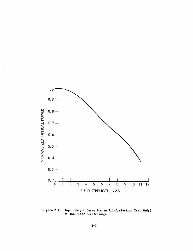
The photograph shownin Figure 2-3 shows the feasibility model, with the
sensor mounted in a lucite tube together with the accessing fiber optic cableand a readout box. No effort was made to miniaturize this model. A
representative curve of output versus applied field is shown in Figure 2-4.
An alternative design is shown in Figure 2-5. In this configuration, the
sensing fiber is placed at the end of a gap or slot between two field-shaplng
pieces of dielectric. The field-induced force arises as a result of locating
the sensing fiber in a strong field gradient created by the dielectric slot.No metal or other conductor is used in the device. Several test models of
this all-dielectric configuration were built, and they all functioned well.
These sensors are best suited to measurement of large fields, 100 kV/m or
more, but they can, with difficulty, be scaled for lower fields, down to
perhaps 10 kV/m.
A number of applications for these unique sensors were discussed with other
workers in the power industry. Examples are briefly described below,
(i) It should be possible to monitor the state of very large circuit
breakers using variations in field near the gap. This field is
dependent on the position of the contacts. It would not be possible
to directly measure contact position with any conventional devices
because of the potentials involved.
(2)
(3)
A 'hot-stick _ with a very simple and robust sensor encapsulated in
it would be a valuable safety tool for service personnel. The
sensor could detect a live conductor on approach and trigger an
alarm signal.
A simple dielectric device that could be manipulated in proximity to
a long insulator string could be used to detect a shorted module in
the strin_ Multiple failures of this type could result in a failure
of the entire strin_ Failure (tpnncture j) detection of this kind
could improve insulator string performance.
A simple test of this idea was conducted at General Electric's High
Voltage Transmission Research Facility (HVTRF) in Pittsfield,
Massachusetts during a visit there last year by JPL personnel.
Detection of a deliberately shorted element in a short insulator was
readily done.
2-5

ORIGINAL PAGE
.OF,,'_R QUALrTY
,i,n, ...... " ....... iPrilI'l III II ........................... 11T11-T
"!rlr Fr ,7_7,,:1 ....lr r=_
lZ:l,.g'_.e 2.-3. Photo_aph of the Fiber Electroscope as Built(the microscope slide base is mounted on a larger
dielectri¢ Iountin$ board)
2-6
1.0
0.9
0.80.7
i 0.6
0.5
0.4
0.3
0.2 I I I I I I I I 1 I I I0 1 2 3 4 5 6 7 8 9 10 11 12
FIELD STRENGTH, kV/cm
Figure 2-4. Input-0utput Curve for an All-Dielectric Test Modelof the Fiber Electroscope
2-7

SPACER
DIELECTRIC ELECTRODE
SPACER
GLASS SUBSTRATE
DIELECTRIC ELECTRODE
Figusr.o 2-5. An All-Dielectric Con£1guration of the Fibex ElectroscopeSensor (No Metal or Conductive Coatings are used)
2-8

:2.3 DC FIELD MBASUREMENT
In contrast to the situation under an ac transmission line, ion current is a
characteristic part of the environment under a High Voltage DirectCurrent (HVDC) line.
The ions of interest are produced by corona processes at the conductor
surface, and accelerated away from the conductor by the electric field. The
density of the atmosphere is such that the subsequent motion of the ions is
dominated by collisions with atmospheric molecules, and an ion of given size
and charge will acquire an effective velocity determined only by the field.
Such motion is usually described in terms of ion mobility. Ions may be
thought of as drifting along field lines, at a velocity given by the product
of the field and the mobility. Any ion current present will flow into a
grounded instrument, or will deposit charge an electrically isolated
instrument. As a result, the instrument must be capable of distinguishingbetween field-induced charge and ion current. With field mills mounted in the
ground plane, the two modulated current components are in phase quadrature,and can be separated by phase sensitive detection (Maruvada, Dallaire, and
Pedneault, 1983). However, the same technique, when applied to a grounded
rotating cylinder field mill (Maruvada et al., 1983) required two sensors
rotating at different speeds to separate the ion current component from the
field-induced output. The device in question had two significant drawbacks.It was large (over a meter in length), and it was grounded.
The sensor described in this report is of the rotating cylindrical field mill
type, but it is quite small, less than 20 cm long and 10 cm in diameter.
Further, it utilizes a fiber-optic readout to isolate the probe electrically
from ground. Therefore, no ion current can flow to the probe in the steadystate. Instead, it will acquire a charge sufficient to prevent additional ion
current from flowing to it. The effects of self-charging due to ion currentare discussed briefly in the following section.
As noted above, instruments capable of measuring electric field at spacepotential have been available for some time for ac use. Similar dc
instruments suitable for use in the field have been described in the
literature, but are not routinely made. Free space dc measurements have been
made in the laboratory using a Pockels crystal (Hikada and Fujita, 1982). The
availability of measurements of dc electric field at space potential will make
possible better evaluation of the field effects due to dc lines, and put dcmeasurements on an equal footing with ac measurements.
2.3.1 Theoretical Background
The principles involved in the design of our electric field sensor can be
understood with respect to Figure 2-6. The external electric field is
determined by measurement of the displacement current between two shorted,
semi-cylindrical rotating electrodes. In the figure, the radius of the
cylindrical electrodes is r, and the split between the two halves is at angle
with the x axis. A uniform field Eo is directed along z and the axis of thecylinder is along y. Under these conditions, the surface charge density a
2-9

Z
v
Fig_e 2--6. Ge_etry of _lit-Cylimler ;ensor Probe
2-10

on the cylinder at azimuthal position 6 is easily derived, and is
given by
o = 2 s E sln0 (2-1)o o
The total charge on the cylinder is assumed to be zero, which means that its
potential is set at the value existing at the location of its axis before itis introduced into the field.
By integrating over one half of the cylinder, the total charge on one of theelectrodes can be evaluated as a function of the electrode orientation angle
= wt. Differentiation with respect to time yields the current i c in a wireconnecting the two half cylinders of length 1:
i = 4 s E I r w sin _t (2-2)c o o
Therefore, if the rotating sensor is placed in a uniform field far from any
conducting surface, its output is sinusoidal, with amplitude proportional to
the field Eo. The current i c is measured electronically and telemetered as a
measure of the field Eo.
A similar analysis, applied to a split sphere rotating about an axis through
the split, yielded a short circuit current i s of
i = 3n s E r2_ cos _t (2-3)s o o
This result is different by a constant factor from the cylindrical case
(is/i c ~ 1,2 for I = 2r), indicating that the finite length of the actualsensor probe does not affect the foregoing argument significantly.
If the sensor is subjected to an ion drift current, it will acquire a charge.
The effect of this charge can be estimated by superposin8 the field from a
charged conducting cylinder and the previously discussed uncharged cylinderimmersed in a uniform field.
The field component resulting from the charged cylinder is independent of O in
the absence of nearby conductors, and, therefore, can make no contribution to
the measured field-induced current i c. Consequently, the sensor will notrespond to a steady-state self-charge if it is far from any conductingsurfaces.
The error introduced by self-charging when the sensor is near a conducting
surface can be estimated using the following argument. Assume that the sensor
is located in a semi-infinite region of uniform field bounded by a ground
plane, with the sensor axis at distance d from the ground plane, and that an
ion drift current flows toward the ground plane. The sensor, assumed to be an
infinite cylinder, will intercept a small portion of the ion current,
acquiring a charge (_ per unit length.
2-11

Under these conditions, the field in the neighborhood of the sensor can be
specified approximately as the superposttion of three components, the unifor_
field (as perturbed by the presence of the uncharged conducting sensor
cylinder), the field of a line charge Q on the sensor axis, and the field of
an image line charge -Q reflected in the ground plane at a distance 2d from
the sensor axis. Additional secondary images resulting from the presence of
the conducting cylinder in the field of the image -Q are neglected.
As we have seen, the field of the line charge on the sensor axis is not
detected by the sensor. However, the field component from the image charge
would be detected, and gives an approximate estimate of the error if the
distance d is large.
In order to estimate the magnitude of the line charge, Oj note that ion
current flow into the sensor will stop when the field component at its surface
due to the self charge Q exactly cancels the field due to the external uniform
field at points on the cylinder opposite the ground plane (0 = n/2 in
Figure 2-6). When this is true, there no longer is a field component at any
point on the surface of the cylinder causing an ion drift toward the cylinder.
Since the field on the top surface of the cylinder at 0 = n/2 in a uniform
field Eo is 2 F o, the condition for charge collection to stop is
2 E = 0 (2-4)o 2_e r
O
It follows that the magnitude of the field Ei at the axis of the sensor due tothe image charge is
o (2-s)Ei = 2nSo(2d)
and the error caused by self-charging obtained by combining equations 4 and 5is
Ri r
E do
for r/d (( 1 (2-6)
Again. an analogous estimate was carried out assuming a spherical sensorinstead of a long cylinder, with the result: " ''
Ei 3 r s
E-- ~ 4 d 2 for r/d << 1 (2-7)O
These two estimates set limits on the error expected for the actual sensor
geometry. Note that the result does not depend on the ion current density.
2-12

It assumesonly that the sensor charges fully, satisfying the surface fieldcondition (Equation 2-4). If full charging does not occur, the error will be
proportionately less.
The above expressions are not accurate if r is not much smaller than d.
Although exact analytical expressions in terms of a series can be derived
using the image method, the slow convergence of the resultant series promptedus to find a numerical means of solving this problem. Using the finite-
element technique, a numarical method was used to find the potential V(x,y)
everywhere within a given enclosed region, provided that the potentials on the
bounding surfaces are known This approach was applied to the problem of an
infinite cylinder near a ground plane.
Because of symmetry, only half of the structure needs to be included. This
region was divided into 260 x 130 equally spaced subregions. Given V1, V2 and
V3 on the bounding surfaces, respectively, the ground plane, the cylinder anda plane surface parallel to the ground plane but far enough from the cylindarnot to influence the results, the potential at each grid point was calculated.
Knowing the voltage everywhere, the electric field can readily be calculated,and the resultant charge on the surface of the cylinder is proportional to the
normal component of the electric field Er there. Summing over all the chargeson the upper half of the cylinder yields the total charge Qu and summing over
all the charges on the lower half yields QI" The quantity Qa = (0_ - Q1)/2 istaken as a measure of the sensor output, since the charge distribution is not
symmetrical when the sensor is near the ground plane.
The fractional change in Qa' AQa/O_o = (Cla - Qao)/(_ao is plotted in Figure 2-7as a function of d/r. Qa A is the calculated value of (t a calculatedfor d/r }} I, that is, with _e sensor in free space.
The quantities AQa/Qao and EI/E o (Equations 2-6 and 2-7) are directlycomparable, and are a measure of the change in sensor output due to the
presence of the ground plane. The condition for charge equilibrium in the
presence of ion current (Equation 2-4), was imposed in calculating AO_/Qao.
It can be seen that a significant change in sensor output can be produced by a
nearby conductor. However, these results indicate that if the sensor is keptat a distance greater than approximately five times its own radius from the
nearest surface, the error will be less than 10_. In addition, estimates made
using a two dimensional cylindrical model are upper limits on the perturbationthat would be seen by a sensor probe of finite length. If the sensor is notmuch closer to a surface than its own length, then the perturbations will be
smaller than the two dimensional model predicts.
The response of similar probes in nonuniform fields has been treated by other
authors (Wilhelay, 1972; tiisakian et al, 1978). Their results show that the
sensor response indicates the field at the location of the center of the probe
before the probe is introduced. Errors of the order of I_ or less were
predicted when the undisturbed field varies by tens of percent over the volume
of the probe. It can be concluded that the dominant error source is image
fields resulting from self-charging when near a conducting surface.
2-13

O
c_<1
0,.
on-O
ZLU
Z
LU
Z<I
2.5 N
2.0
1.5
1.0
0.5-
0.0
Figure 2-7.
GROUND PLANE
FINITE ELEMENT CALCULATION
I I I2.O 3.0 4.0
RATIO OF DISTANCE OF CYLINDER TO GROUND TORADIUS OF CYLINDER, d/a
Fractional Change in Sensor Output Induced _a
Nearby Conducting Surface for Full Ion Current
Qharsins
2-14
IE
|It
ir.
#
!
=-
z
J
2.3.2 Sensor Design
The overall instrument consists of two parts: (1) the sensor probe, which isself-contained and isolated from ground, and (2) a set of readout electronics,
providing an output suitable fox use by a data acquisition system. The two
parts are connected by a conventional 100 micrometer diameter core multimode
fiber optic cable. .The overall cable diameter including strength members isabout 3 mm. ...... -_ ";
The unconventional aspects of the instrument are located in the sensor probe,
which will be briefly described. A stationary tube supports the rotating
sensing head, and carries a small battery powered dc motor to drive the
surrounding rotating element. The rotating element contains an electronics
package, powered by separate watch-type batteries, which measures both thedisplacement current between the two electrodes and the position of the
rotating part of the sensor with respect to the stationary part. This
information is encoded in terms of pulse repetition frequency and used todrive an LED transmitter.
A rotary optical coupler transfers information from the rotating electronics
into a non-rotating fiber cable termination mounted on the axis of the
supporting tube. No use is made of slip rings or rotary transformers.
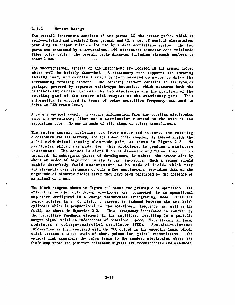
The entire sensor, including its drive motor and battery, the rotating
electronics and its battery, and the fiber-optic coupler, is housed inside the
split cylindrical sensing electrode pair, as shown in Figure 2-8. No
particular effort was made, for this prototype, to produce a miniature
instrument. The sensor is about 8 cm in diameter and 20 cm long. It is
intended, in subsequent phases of development, to reduce the sensor size byabout an order of magnitude in its linear dimensions. Such a sensor should
enable free-body field measurements to be made of fields which vary
significantly over distances of only a few centimeters, providing data on the
magnitude of electric fields after they have been perturbed by the presence ofan animal or a man.
The block diagram shown in Figure 2-9 shows the principle of operation. Theexternally mounted cylindrical electrodes are connected to an operational
amplifier configured in a charge measurement (integrating) mode. When thesensor rotates in a dc field, a current is induced between the two half-
cylinders which is proportional to the rotational frequency as well as the
field, as shown in Equation 2-2. This frequency-dependence is removed bythe capacitive feedback element in the amplifier, resulting in a periodic
output signal which is independent of rotational speed. This signal, in turn,
modulates a voltage-controlled oscillator (VCO). Position-reference
information is then combined with the VCO output in the encoding logic block,
which creates a coded train of short pulses for optical t_ansmissio_ Theoptical link transfers the pulse train to the readout electronics where the
field amplitude and position reference signals are reconstructed and measured.
2-15

PAGE'
I_ _ QUALITY
DRIVE
MOTOR BATTERY _--_ -
.... BATTERY
ELECTRODE\
FIXED HANDLE \
\-
HOLDER ........
DRIVE MOTOR _NICS/ _RD
F
LIGHT ;-
EMITTING _.DIODE
10 cm
=
L
Figure 2-8. Photograph of the Prototype Sensor with One-Half
Cylindrical Shell Removed to Show Internal Parts
2-16

SENSOR
PLATES
I INTEGRATING
AMPLIFIER
REFERENCE
POSITION
SENSOR
V
v
VOLTAGE
CONTROLLED
OSCILLATOR
_FLv
FIBER OPTIC CABLE
ENCODING
LOGIC
LED WITH
ROTATING
REFERENCE
POSITION
DECODER
COUPLING
RECEIVER
MODULE
OSCILLOSCOPE
OR LOCK-IN
AMPLIFIER
SIGNAL
DEMODULATOR
DVM
Figure 2-9. Functional Block Dia_rem of the Sensor Electronics
2-17

2.3.3 Position-Reference Encoding
The position-reference signal is needed in order to obtain the angle of theelectric field vector as well as its magnitude. In this design, a
phototransistor on the rotating part of the sensor passes in front of a
stationary light-emitting diode (LED) once every revolution, sending a
signal to the encoder to mark the reference position. The optical
transmitter normally generates a short pulse (0.25 ps) at each positive
transition of the VC0 output. When the slgnal from the position-reference
phototranslstor is received, the next optical pu_se is replaced by two
pulses in close succession The addition of the reference pulses to thedata-pulse train does not disturb the amplitude signal, and gives an average
angle resolution of 1.5 degrees (at 2400 rpm).
2.3.4 The Optical Link
The optical link consists of an LED transmitter, an appropriate length of
fiber-optic cable, and a receiver module with a built-in amplifier. A
standard fiber-optic connector was modified to provide the rotary
coupling between the sensor and the cable. The encoding format, a very low
duty-cycle pulse frequency modulation, was chosen to conserve battery power,
with the object of increasing the duration of operation of the instrument.
A schematic of the sensor head and the receiver system is shown in
Figure 2-10. Figure 2-11 shows the sinusoidal output, as seen at thedemodulator output of the receiver for adc field at the sensor head of
30 kV/L
2.3.5 Laboratory Evaluation
Laboratory evaluation of the sensor gave the following results:
(i) Direct fields ranging from 70 Vim to 50 kVlm, a dynamic range of
roughly 103, were measured using an ac voltmeter to read the output
voltage. Within the above range the sensor was linear to
within 2_.
(2) The measured ac output voltage was independent of frequency (within
I_) over a range corresponding to sensor speeds between 600 and
4200 rpm, as shown in Figure 2-12. _ith a new 9 V battery, the
sensor rotates at approximately 2400 rpL
(3) The current drain of the rotating circuitry was less than 1.4 mA at
6 _ This was measured with the encoder driving the LED with
40 mA pulses at a center frequency of 10 kHz, giving an optical
power margin of 6 dl_ The LED accounted for less than I0_ of the
total current drain The pulse-coded fiber opti_ data readout does
not dominate the power requirement of the rotating circuitry. The
present power drain is approximately 8 mW, but an optimized design
could reduce it significantl_
Taken together, the results of the laboratory tests show that the sensor is
capable of measuring the field-induced charge on its electrodes within ~2k
2-18

/ I047#F Ih_-. I V
"_ _ ' 1 n ,>lOOK I---'----" _ \_J XMTR
/ _ - icA342o___j cD _SlSl I'1o_ I 1_o ' -v
(POSITION SEN SO R) 100-g $100K.g
-V _ I I _ +V COMBINING LOGIC
Figure 2-10a. Schematic of DC Field Sensor Probe
2-19

+6V
+6V 1K _
I:tBER CABLE RED +6V
HEAD J IE 3 2
_LB LACK
OPTICALRECEIVER
+6V
+6V100 K +6V
11
-T, °'I:----I I I LSEOUT T
+TR Q2_
330K - 2000PF iM.011_ F
DUTY CYCLE EXTENDER
POSITION PULSE DECODER i14 +6V
13
10M
CD4046
+6V
0.1 f_F PLL FREQ. SYNTHESIZER(36 x POSITION PULSE)
1100PF
PLL FM DEMODULATOR
1OK
14 13
1 3
12 1M
10_ZERO CROSSINGDETECTOR
DEMODULATOROUTPUT
+3V b,_ r_I"
CD4046
1500PF
+6V
DIGIT 2 DISPLAY DATA
Figure 2-lOb.
-_50"lpF
10K +6V
15
j CLR 5
74HC112 QCK
2K
DISPLAYSETUP "="
LOG IC
DIGIT I
DISPLAYDATA
DI C I B I AI
TO DISPLAYLATCHENABLES
"360" RESET
7 LOGIC
SchemaLic of DC Field Sensor Receiver
J
!i+i!i
iII
!!i!
ii
I!
|!i!I|
!I!
!
i
!
!
2-20

ORIGINAL PAGI_ IS
OF POOR QUALITY
Figure 2-11. Typical AC Output as Seen at the Receivez
2-21

5OO
45O
4OO
350
_>
300
S 2.50
O 200U.<
150
100
5O
v AA A
m
I I I I 1 I I10 20 30 40 50 60 70 80
INPUT FREQUENCY, Hz
Fisure 2-12. Output of Sensor at Rotational Frequencies Corresponding
to Speeds between 600 and 4200 rim
2-22

2.3.6 FIELD TESTS
The prototype sensor was taken to General Electric*s High Voltage TransmissionResearch Facility (IlV_F) near Pittsfield, Massachusetts, for evaluation in a
more realistic environment using facilities described in earlier reports(Comber and Johnson, 1982; Comber et al., 1983). Three types of measurements
were undertaken: (1) sensor response in a large test chamber used for field
calibration, (2) a field survey under a --ipolar dc transmission line, and (3)
demonstrations of the kind of measurements possible only with an isolated
sensor: measurements of the field above the permanent equipment at the
measurement location, and around a person standing directly under the line.
The results of these initial measurements are given in the followingparagraphs.
As was pointed out earlier, the environment around a full-scale transmission
line is characterized by space-charge and ion current, as well as the electric
field. _he space-charge significantly modifies the electric field, and the
magnitude of the space-charge field varies with time and weather conditions.
Of more concern to free space field sensing, the ion current will deposit
charge on any electrically isolated object, including the sensor and its
supporting dielectric pole. The effect of the collected charge on the field
measurement must be understood in order to make dependable and accurate field
measurements. As will be seen, the data obtained in the test cage do show a
response which is thought to be due to self-charging, although its magnitudeis not large.
The sensor response was determined in a planar test cage which had a 92 cm
spacing between the ground plane and the energized electrode. The cage wascylindrical, approximately 3 m in diameter (Comber et al., 1983) and had two
peripheral grading rings to minimize the effect of fringing. The sensor was
placed on the axis of the cage approximately 30 cm above the ground plane.
For this measurement, and for those described below, the sensor was supported
by a fiberglass pole 2.5 cm in diameter and 3 m in length. The pole was
oriented along the projected axis of the rotating sensor, although there was asmall (~ 2 cm) offset between the axis of the pole and the axis of the sensor.The surface resistivity of the pole was not known.
The calibration curve obtained in the cage is shown in Figure 2-13. The
applied field, shown on the abscissa, is based on measurement of voltage andelectrode spacing. The plot represents one excursion from zero field to
maximum and return. The indication from a separate field probe (MonroeElectronics) located in the ground plane of the test cage is consistent with
the small hysteresis loop seen in Figure 2-13 and the droop of the curve below
a linear response being due to self-charging of the sensor probe, or the pole
used to support it. The magnitude of the perturbation averaged 3_,. No
attempt was made to monitor field direction in the test cage.
The second set of data, shown in Figure 2-14, was obtained in order to
illustrate the type of field-mapping above the ground plane which is possibleonly with an electrically isolated probe.
2-23

>E
I-::)
I--
0_J<
700 -
600
5OO
400 -
300 -
200 -
100 -
0,0
1 I I I I I I I I I J5 10 15 20 25 30 35 40 45 50 55
DC FIELD, kV/m
r
Fisur e 2-13. Calibration Oarve Obtained in HVTRF Test Cage
2-24

Field measurements were made around a person while he was standing directly
under the conductor of the short test line at the IlVIRF. 1]ae fiber glass pole
was counterbalanced (for convenience) and the field readings were noted on a
large Polaroid photograph which included the test subject. The sensor is
shown in Figure 2-15, held by Dr. Gary _ohnson of HV]RF. The test subject is
Bj6rn Eng of 3PI_ The conductor was charged to -200 kV dc for thisexperiment, which yielded an average field at ground level directly under the
conductor of 7.7 kV/m, and an ion current density varying between 0.5 and
5.0 nA/m 2 as measured by the IIV]RF data system located in the ground plane.
The prototype sensor measured 6.2 kV/m at 1/2 m above the ground surface
without the human subject being there.
In the figure, the length of each arrow indicates the magnitude of the fieldas measured at the location of the arrowhead. The sensor, attached to the 3 m
fiberglass pole, was held stationary for a short period of time (~ 10 sec) at
each position indicated in the figure. One of the investigators recorded the
output of the sensor, while another noted the location of the sensor. To
facilitate estimating the sensor position, a large-format instant photograph
was made, and a grid was drawn on it, The position of the sensor probe was
noted in terms of grid coordinates by reference to the photograph. The uncer-
tainty of the position was roughly + 5 cm. Figure 2-14 was later produced
from this photograph, by combining the appropriate position, amplitude, and
direction information Field direction was measured vianally on an oscillo-scope (by a third investigator), using the phase of the angular position
reference signal transmitted from the rotating sensor head. The direction
measured without the person being present was assumed to be vertical and usedto calibrate the position output. The accuracy of field direction was roughly
+ 20 o. Instrumentation for precise, direct readout of field angle has subse-
quently been completed. The observed field at a location 20 cm above the head
was 20.8 kV/m, 3.4 times the undisturbed field at ground level
For comparison to the measured values, field intensification over a conducting
prolate ellipsoid, placed with its axis perpendicular to a conducting ground
plane and its center on the ground plane, was calculated as a function of the
aspect ratio of the ellipsoid and the height above the ellipsoid surface. On
the top surface of the ellipsoid, corresponding to the top of the head, a
field intensification by a factor of 23 was obtained for an aspect ratio
(metal-major axls/seml-mlnor axis) of 6, and 13 for an aspect ratio of 4.
These results compare to a factor of. 12 to 14 at the forehead reported by
Silva et. al., (1985) and a factor of 18 reported by Kaune and Phillips(1980), both for ac fields. However, the calculated field intensification on
axis, at a distance of 20 cm above the top surface of an ellipsoid with semi-
major axis 2 m, was between 3 and 3.5, and not sensitive to aspect ratio, in
agreement with observation.
The field intensity observed over the head was reduced to 9 kV/m when the
subject was wearing a plastic hard-hat, and with no other change. This
reduction is thought to be a result of charge deposited on the dielectric
helmet. It appears likely that the electric field around a human subject can
be modified by charge deposited on the hair and clothing by a de ion current.
The presence of charge on the hair was clearly observed on several of the
investigators during the course of these measurements.
2-25

W+.O°+.A.O.A+_qWITH HARD-HAT
Figure 2-14.
_"°-'_ I __.2oo
_III-11.6
(
IIBo_1188.0 "-*" 1 --4.0
5.2"_
Electric Field Vectors Measured Near a Test Subject
(Measurement Point Is at Head o£ Arrow)
2-26

ORIGINAL PAGE ISOF pOeR QUALIFY
Figure 2-15. Measurment of Eleotrte Field in the
Vicinity of a Person
2-27

]he third set of data, shownin Figure 2-16, shows the response of the sensor
as a function of time, at a fixed location directly under the dc conductor and
0.6 m above the 8round_su_rf_ce. The conductor voltage was changed
from -200 kV to -500 kV during the interval between the one minute and the two
minute marks in the figure, and remained constant after that.
_he field at ground level as measured by the HV]RF instrumentation is also
shown in the figure for comparison. The ion current, also measured by theIlV_RF instruments, varied between roughly 20 and 170 nA/m 2 during the period
of measurement, the changes being due to a light and variable wind transverse
to the test line. The magnitude of the ion current that would have been
collected and measured by the field probe, if it had been grounded, was about
three orders of magnitude smaller than the current induced by the electric
field. O, anges in the field with time, as measured with the two instruments,
correlate well The prototype sensor yielded a lower field value by about
15_, on the average.
Similar observations were made by Maruvada et a1.,(1983) using two
independently calibrated instruments, one a ground plane field mill, and theother a large split cylinder probe. He also observed a lower field, by
approximately the same amount under the same test line at the IIV_J_, although
anothez comparison involving severai instzuments-_ows no similar systematicdifference for all the instzt, ments (Comber et ai., i983).
A number of possible error sources were examined durin $ analysis of the data,but none were found to be i arge enough to explain the observed difference.These included error due to self-charging of our prototype sensor, either in
the calibration cage or under the test line, charge accumulation or leakage
along the flberglass supporting pole, and instrumentation errors.
To calibrate the HVTRF fixed-location field meters, a vibratin 8 plate
electrometer, mounted in a 1 m2 _pl_-a-te, was first calibrate_d in the test cage
and then Piaced on the ground adjacent to. the fixe d iinstr_enta_on, where i£was used as a transfer standard. It is felt that the 15_ difference between
the prototype sensor and the HV_RF instruments may represent a nonuniformity
of the field near the ground surface in the measurement area, inclnding the
temporary location of the transfer standard. To illustrate this explanation,
Figure 2-17 shows the field intensity as measured 0.6 m above the ground
surface along a line parallel to the HVDC conductor and crossing the line ofinstrumentation.
The horizontal scale in the figure is approximate, but the relative location
of the elements of the HVIRF instrumentation is correctly noted. Variations
in the electric field of the required magnitude are seen, especially over the
slightly raised ion current sensing plates, as expected. These variations
cannot be due to self-charging or calibration errors in the isolated-probe
sensor. However, if the effective_ground plane surrounding the transferstandard were depressed below the 1 m_ aluminum plate in which it was mounted,
or if a local depression of the effective ground existed under our prototype
sensor, distortion could occur that would explain the discrepancy.
2-28

E>
_1I11
I1
aIIIrt-
U3<111
35
3O
25
20
15
10
0
I PROJECT UHV DATA SYSTEM
JPL DC PROBE
I I I I I I I I I I I I
0 1 2 3 4 5 6 7 8 9 10 11 12
TIME t MIN AFTER 17"23
I
13
Figure 2-16. Electric Field Versus Time Measured Under DC Conductor,
Compared to HVIRF Data
2-29

E>
._1W
In
13CI--
W_I1,11
15
10
5
0
m
n
i- FENCE FIELD ION CURRENT TALL GRASS
SENSOR SENSOR _ _
POSITION, PARALLEL TO TEST LINE
Figure 2-17. Measured Field Values Along a Line Crossln8 PermanentInstrn_entatlon, 0.6 u Above 6round
2-30

2.3.7 SELF-CHARGING EXPERIMENTS
A detailed investigation, both analytical and experimental, of the effects of
self-charging of the sensor is underway, with the goal of understanding
quantitatively the errors induced b_ charge accumulation in a space-chargeenvironment. - "
The space a_ormd high-voltage conductors where field measurement is likely tobe of interest normally conducts a significant ion current. The sensor is
electrically isolated in order to allow field measurements far from the ground
plane. This combination of an isolated sensor subjected to space charge
current has not been previously analyzed.
_he parameters of interest are, first, the influence of a conducting surfacenear the sensor, and second, the potential of the sensor itself, or more
precisely, the potential difference between the sensor and the free space
potential at its location. This voltage difference will be referred to as the
excess voltage of the sensor, l_e dc sensor described above was placed in a
specially configured test cage for experimental measurements, and theoreticalcalculations to confirm the results are still in progress.
2.3.7.1 Experilental Test Arrangement
Before the dc sensor could be evaluated for the effects of self-charging, a
means of producing a miform dc electric field with negligible space charge
was needed. A test cage arrangement similar to those used elsewhere to
calibrate ac field strength meters was designed and constructed. This
arrangement consists of two parallel electzodes of equal size separated and
supported by dielectric rods.
The dimensions of the test cage and clearance distance between the cage and
surrounding conductors was determined after taking into account published
material by Takuma, Kawamoto and Sunga (1985) which analyzed field variations
within a test cage. The dimensions selected for our test cage are expected to
keep distortion to within 2% at the sensor location.
The field cage was made from two 6 ft by 6 ft aluminum screens, separated by
one meten This assembly was supported one meter off the ground, and at least
one meter away from any surrounding conducton Additional dielectric supports
outside the cage were used to prevent the screens from sagging, since
significant deviations from a uniform field would otherwise occu_ Sharp
edges and corners of the screens were coated with silicone rubber to eliminate
Corona.
The upper screen was connected to a variable negative $0 kV dc supply via a
feed line parallel to and in the same plane as the screen. The lower screen
was similarly connected to a variable reversible polarity 30 kV dc supply.
Screen potentials were carefully monitored using separate high voltage probes.
With both supplies adjusted to their maximum output, corresponding to a
70 kV/m field, no noticeable corona was observed. The test cage and thesensor mounted in it are shown in a photograph, Figure 2-18.
2-31

ORIGINAL PAGE iSOF POeR (_AJALrTY
Figure 2-18. Field Case and Test Benoh Arrangeeent(Inset Shows Sensor Without Tubes)
2-32

A special test bench, seen in Figure 2-18, was constructed to support and
manipulate not only the sensor by itself, using its fiberglass support pole,
but also to hold two stationary 6 ft aluminum tubes extending from each end ofthe sensor. These tubes, which have the same diameter as the sensor, were
adjusted to be coaxial and within 3 mm of each end of the sensor to
approximate the Infin/te cylinder geometry treated in the analysis.
2.3.7.2 Parameter Measurements
Prior to the self-charging experiments, a ltnearity test of the sensor outputversus electric field was made. The sensor was positioned in the center of
the cage (without the tubes) while its output was measured for fields ranging
from 1 to 60 kV/u_ Within the above range the sensor was linear to within 1%
as shown in Figure 2-19.
With the cylindrical tubes added to the arrangement, measurements were taken
with the axis of the sensor at different distances above the bottom screen,ranging from a minimum of 1_ sensor radii to a maximum of 13.1 radii at the
center of the cage. During these measurements, the extension tubes and the
sensor were both grounded to ensure that its potential was known. The
connection to the circuit ground on the rotating electronics package was made
by means of a brush and slip-ring assembly.
While maintaining the field in the cage at 30 kV/m +1% the variable supplies
were manipulated to create different excess voltages at the sensor.
Figure 2-20 shows how one such excess voltage was produced.
Figure 2-21 shows the observed variations in sensor output as a function of
excess voltage and distance from the lower plane of the cage. In the case
where d/r is 12, the gap between sensor and conducting plane is only 02r.As can be expected in this case, measurement error due to field distortion
between sensor and plate is large. In the case where d/r is 5:25, the surfaceof the sensor is 16 cm above the conductor (or about 6 inches) and the error
has been reduced to less than 10_, even with excess voltages as great as 2kV.
From the data above, graphs were made which plot fractional change in sensor
output as a function of d/r, both for an uncharged sensor (excess voltage
zero) and for a sensor charged to an excess voltage of -2.64 kV. An excess
voltage of -2.64 kV was determined through preliminary finite element
calculations to be the equilibrium potential to which the sensor would chargein this field if subjected to a space-charge current. Figure 2-22 and
Figure 2-23 show some of our measurements.
The entire experimental procedure described above was repeated with the
extension tubes removed. The only observed difference was an increase in
scale factor of approximately 25_ when the extension tubes were removed. The
two factors creating this increase are field fringing in an axial direction at
each end of the sensor, and the effect of the curved anti-corona shells on theend of each electrode. Both of these effects increase the effective area of
the electrodes. The magnitude of the observed increase in scale factor is in
agreement with an analytical estimate.
2-33

400
5
_ 300
_ 200
100
01 5 10 15 20 25 30 35 40 45 50 55 60
ELECTRIC FIELD, kV/m
Figure 2-19. Measured Sensor Output as a Function of Electric Field
2-34

UPPER SCREEN V 1 = -26 kV
,_ =J N1
Ir
SENSOR
AXES --_
_ FOR d/r=2.6
r = cm
t V2 = +4 kV
E- Vl ,_-V2 _ -26kVlm- (+4 kV) -- 30kV,/m
VEXCEss¼V 2- _E.d] :+4kV- [30kV/m' 0.991m] :+1027V
Figure 2-20. Example Showing Arrangement Used to Produce an ExcessVoltage of +1027 V on the Sensor
2-35

4OO
300
100
cl/r = 1.2
2.62
5.25
13.12
-2000
I I I I
-1000 0 +1000 +2000
VEXCESS, VOLTS
Figure 2-21. Sensor Output vs Sensor Excess Voltase for VariousRatios of d to r, E Field Constant at 30 kV/:
2-36

I60%
5O%
0%1 2 3 4 8 9 10 11 12
RATIO OF DISTANCE OF SENSOR TO SCREENTO RADIUS OF SENSOR_ d/r
14
Figure 2-22. Measured Chanse in Sensor Output as a Function of
Distance to Screen, Sensor Uncharged
2-37

300%
o
o
=)
0
0
Z1.1.1
Zm
I,,LI
0Z<"r"u
200%
150%
100%
50%
0%1 2 3 4 5 6 7 8 9 10 11 12
RATIO oF DISTANCE OF SENSOR TO SCREEN TORADIUS OF SENSOR, d/r
Figure 2-23. Measured Change in Sensor Output as a Function ofDistance to Screen, Sensor Fully Charged (-2.64 kV)
2-38
13 14

2.3.8 CONCLUSIONS
Initial laboratory and field experiments have shown that electric field
measurements in free space above the ground plane can be readily made with an
electrically isolated probe which is small and portable. Experimental and
analytical work to date indicates that readout of induced charge with 2_
accuracy will be readily achievable, and that image fields due to self-
charging in the presence of nearby conductogs will not unduly limit accuracy.In addition, it was possible to measure the electric field vector, that is,
both magnitude and direction of an unknown field, at locations above the
ground plane with the sensor.
It should be noted that the same sensor has been used to measure ac (60 Hz)
fields simply by stopping the spin and reading out the 60 Hz component of the
output signal. Field direction for an ac field could be determined from the
internal position reference with appropriate instrumentation using, for
example, a spin rate small compared to 60 Hz (say, 80 rpm). Experimentalresults obtained in ac fields will be reported on later.
Further work on this sensor will focus on refinement of the sensor design,
with the goal of reducing the size and easing the requirement for frequent
battery change. Analysis indicates that the induced charge can be detectedwith adequate accuracy on an electrode area as small as 1 cm 2 with good
electrometer amplifier desif_ For example, referring to Equation 2, with
applied field Eo = 100 V/m, a = 0.5 cm, 1 = 2 cm, and w corresponding to
20,000 rpm, the field-induced current i c is I hA, well within the reach ofgood semiconductor electrometer amplifier design.
2-39

_L
EE
LL

SECTION 3
FIBER OPTIC TEMPERATURE SENSING
One area where fiber optics can make possible a power system measurement that
has not previously been made is the distributed sensing of temperature in
electrical apparatus. There are three areas withinpower systems where such ameasurement would be of considerable value: overhead phase conductors,
underground cables, and station equipment. Each of these areas w illbe
discussed in turn
3.1 APPLICATIONS
3.1.1 Overhead Phase Conductor Temperature Measurement
Since any electrlcal conductor at normal temperatures has a finite resistance,the current that it transmits causes it to dissipate heah The temperature of
a heavily loaded phase conductor varies according to the wind speed and
dlrectio_ and according to the current that it is carrying. Because of this,
it probably varies from span to span The hottest span in the llne (wherever
that may be) determines the thermal rating for the line. Since the hottestspan is not, in general, known during operation of the line, the thermal
rating is based on a statistically developed table of line capacity against
ambient temperature. This is, of necessit_ somewhat conservative.
If a fiber optic cable could be installed so as to measure the temperature
along the phase conductor, it would be possible to develop a dynamic thermal
rating system. A system of this sort would allow the line ampacity to bedetermined accurately based on measurement. This would result in improved
utilization of equipment, and, therefore, of the capital investment associated
with the equipmen_
To be of maximum use, the fiber optic cable has to be installed on existing
conductors. This can be accomplished by placing the fiber optic cable around
the existing conductor, probably within a tube of plastic. The relation
between the temperature seen by the fiber and the temperature inside the phase
conductor would have to be determined carefully.
The use of small objects wrapped around the larger phase conductor in this wayhas been likened to the action of a aerodynamic spoiler, and is said to have
advantages in terms of controlling aeolian line vibration and ice galloping.
Overhead lines frequently go for distances in the order of 50 kilometers
without being tapped, and, consequently, a temperature measurement system must
be able to reach distances in this order of magnitude. It will be seen later
that this tends to limit the number of ways in which temperature can bemeasured.
3-1

3.1.2 Underground Cable Temperature Measurement
Knowledge of the temperature distribution along an underground cable offers
potentially the same benefits as it does in the case of an overhead conductor.
The circuit can be operated closer to its thermal limit in the steady state,
and emergency operation at higher temperatures may be possible, since the
ability of an underground cable to carry an overload is strongly dependent on
the temperature when the overload begins. Unlike the case of an overhead
conductor, however, which will sag as it gets hot, the underground cable is
supported along its length, and cannot move at all. However, operation at
high temperatures is knows to degrade the insulation and shorten its life.
Under present circumstances, operation of cables is perhaps even moreconservative than overhead lines.
There is considerable interest in know in 8 the temperature profile of pipe-type
cables, in which the three phase conductors separately are inserted into a
pipe filled with dielectric fluid (oil). A know ledge of the temperature
profile along the line will permit the evaluation of the effectiveness of
attempts to improve the cooling by circulating the oil, or other measures.
Normaliy plpe-type cables are spliced at distances not in excess of two
kilometers. Consequently, a system of temperature measurement might only have
to reach that distance.
3.1.3 Power System Equipment Temperature Monitoring
There are a number of potential applications for fiber optic temperature
monitoring inside power system equipment. Of particular interest aremeasurements which will enable the determination of winding hot spots in
transformers and reactors, and the temperature distribution of surge
arrestors.
In new transformers, the fiber could be integrated with the winding or
incorporated in the winding duct spacer. In existing units, the fiber could
be threaded through the cooling ducts or placed on the outside of the winding.
The exact location of the fiber would also influence whether the fiber was
exposed to an electrlcal stress as well as temperature effects. This in turn
might affect the method chosen for the measurement.
The distance that would need to be monitored for an understanding of the
temperature distribution inside a piece of power system equipment is the
shortest of the three applications considered here. It would probably notexceed a few tens of meters even if the fiber were wrapped around the
transformer winding a few times.
i!
3-2

3.2 METHODS OF MEASURING TEMPERATURE DISTRIBUTION
In order to measure any parameter (including temperature) as a function ofdistance, some form of reflectometer is needed. A reflectometer can be
thought of as a kind of radar operating down the optical fiber. Radar of the
kind used at airports operates in free space. The velocity of radio waves infree space is a constant. It is therefore possible to calibrate the radar
reflections in terms of their distance from the transmitter. The reflection
of a pulse a certain time after it was transmitted yields directly thedistance to the object which caused the reflectio_
In cables, whether optical or radio type cables, the velocity of transmissionis lower than the velocity of light in free space, and the calibration in
terms of distance is more difficult, although, in principle, if all the
parameters of the cable are known, it can be done. For this reason,
reflectometers operating in cables are conventionally referred to as time-
domain reflectometers. In fiber optics, since the pulses are optical rather
than of radio wavelengths, the device used is known as an optical time-domainreflectometer.
An optical pulse launched into a fiber will be transmitted through it almost
unchanged for the entire length of the fiber. It will be slightly changed,however. At any particular position there will be some reflection of the
energy in the pulse. Some of the energy is scattered by the molecules of the
glass, a phenomenon known as Rayleigh scatterin_ (The energy returning to
the sending end in this manner is said to be backscattere&) This effect,
while small, does mean that the pulse is slightly attenuated as it proceeds
down the fiber. The curve of reflected power (measured by the OTDR from thebackscattered energy) as a function of time (or distance) as seen on the
display of the OTDR will, therefore, inevitably show some droop. Anydiscontinuity in the fiber will show up as an excess loss over and above this
normal droop. In this way, it is possible to test the quality of splices andconnectors in fiber optic systems, an application in which the OTDR is
invalunble. Figure 3-1 shows an OTDR system and its output from a samplecable.
Another way in which the pulse lannched into the fiber is changed during itstransmission is its tendency to spread out due to the various kinds of
dispersion occurring in the fiber. (See Kirkham et al. (1984) for a detailed
explanation of dispersion.) In an ordinary telecommunications application,
dispersion limits the bandwidth-distance product of the fiber, that is to say,it provides an upper limit on either the distance or the bandwidth for whichthe fiber can be used.
For our application in measuring the position of a hot spot, dispersion will
limit the accuracy with which the position of any discontinuity in the fiber
can be determined. Based on the approximation that in free space light
travels about one foot in one nanosecond, one can develop the rule of thumb
that a pulse which is spread to a microsecond in width in an optical fiber
cannot give the location of any discontinuity to an accuracy better than a fewhundred feet.
3-3

OPTICALPULSE
SOURCE
OPTICALRECEIVER
OPTICAL
. >>CONNECTOR
ELECTRICAL SYNCHRONIZING
SIGNAL L!DISPLAY
OPTICAL FIBER UNDER TEST l
a) Optlcal Time-domain Reflectometer
CONNECTOR
REFLECTEDPOWER
LIGHT PULSELAUNCHEDINTO FIBER
FUSIONSPLICE
COUPLER FEEDTHROUGH
I I
BACKSCATTER
LOSS IN SPLICE
REFLECTION FROM CONNECTOR
LOSS IN CONNECTOR
LOSS IN MICROBEND
FRESNEL ENDREFLECTION
MICROBEND
FIBEREND
DISTANC_
LAUNCH ........
b) OTDR display
Figure 3-1. Optical Time Domain Reflectometry
SYSTEM NOISE
TIME
:3-4

To obtain the temperature profile of a fiber, the OTDR display can be used to
show temperature as a function of distance, rather than loss as a function of
distance. To do this, the temperature must be related to the loss, or to some
form of reflectivity, in some known way. The OTDR display could then be
calibrated directly in terms of temperature. Temperature resolution is set by
the ability of the OTDR to distinguish between two values of loss. Areasonable value here is 0.1 dB.
Distance resolution is a function of the width of the pulse launched into the
fiber, and the dispersion. Since the effects of dispersion increase with
distance, the resolution will deteriorate with 'reach' for a given OTDR. For
a 2 km reach, a resolution of 10 nsec (about 3 m) should be possible,
depending on the fiber.
Distributed temperature can be sensed through a number of possible mechanisms
using an optical time-domain reflectometer. These include temperature
dependence of birefringence, temperature dependence of losses, couplingvariations with temperature, temperature dependence of core-cladding index
ratio (or numerical aperture), optical effects in temperature sensitive
compounds (particularly organic compounds), and simple temperature dependence
of optical index. Each of these approaches will be discussed in turn.
3.2.1 Temperature Dependent Birefringence
Certain materials exhibit a different refractive index for two orthogonal
polarizations of light. Materials exhibiting this property are said to be
birefringent. Normally, one considers two orthogonal linear polarizations,
one exhibiting the fastest propagation velocity in the material and the other
(orthogonal to it) exhibiting the slowest propagation velocity. If the
birefringence can be made temperature dependent, then, in principle, the
temperature can be sensed along the fiber. The different transmission
velocities of the two orthogonal components will result in their having a
phase relation which varies as a function of temperature. Analysis of the
reflected information for a sensor of this type will be a little more
complicated than for a straightforward optical time-domain reflectometer.
However, the equipment shown in Figure 3-2 can probably be arranged to provide
a readout of temperature as a function of distance.
Until recently, fibers which preserved the state of polarization were notavailable. While they are currently being manufactured, the temperature
dependence of the birefringence has not been investigated. Therefore, while
this approach, at least in concept, can give a temperature distribution
sensor, it must be regarded as somewhat high risk at this point.
3.2,2 Temperature Dependent Loss
Normally, the glass used in making a fiber is extremely pure, because
impurities have been found to cause loss of optical power. By deliberately
doping the glass with a suitable material, however, it is possible toconstruct a fiber in which the loss varies as a function of temperature. This
may be the simplest method of measuring temperature, and may require the least
3-5

POLARIZED
SOURCEi,
BEAMSPLITTER
POLARIZATION I [
ANALYZINGDETECTOR J t
PROCESSOR ]PHASE RELATION OF ORTHOGONALPOLARIZATIONS DEPENDS ON
BIREFRiNGENCE
Figure 3-2. Birefringence Sensing
3-6

development. The transition metals, such as Cu, Fe, Ni, Co, and Cr have ions
that will absorb photons at the visible and infra-red wavelengths of interest.
Doping with one of these materiels would seem like a reasonable place tostart.
As explained in an earlier JPL report (Kirkham et al., 1984) microbendlng
represents an excess loss in many fibers. In some implementations of
microbending sensors, the bare fiber stripped of buffer is deliberately
exposed to pressures from a micro-anvil which causes the loss. In the
anticipated implementation of a temperature dependent microbending loss
sensor, the buffer remains on the fiber and is deliberately made to have
different physical temperature sensitivities than the fiber itself. As a
result of this, a temperature change in the buffer/fiber system induces a
mechanical force on the fiber which results in the required excess loss. The
arrangement is shown in Figure 3-3.
While excess loss of this type has been observed, for example, in some of the
early communications fibers, its mechanism is not well understood and has not
been investigated thoroughly. It might be fair to say that the effect was
observed as a nuisance in the early days of communications fibers. Subsequent
work done on it was aimed at reducing or ellmlnatlng its effects.
3.2.3 Coupling Variations With Temperature
If two fibers are run in close proximity for a considerable length, some of
the energy initially launched into one fiber will be coupled into the other.
By choosing the appropriate physical construction, the degree of coupling can
be made temperature dependent. The implementation then becomes a variation of
the basic optical time-domain reflectometer in that the energy is launchedinto one fiber and the reflections are received from another.
It is possible to implement the arrangement in a number of ways, one of which
is shown in Figure 3-4. For example, a multicore fiber can be constructed, or
two separate fibers can be encased in the appropriate polymer buffer, or othercombinations of materials can be use&
3.2.4 Temperature Dependent Optlcal Index Ratio
The efficiency of an optical fiber depends on the ratio of the refractive
indices of the core and the claddin 8 material Normally, these two parameters
differ only by a few percent. If the refractive index of either the core or
the cladding is made temperature dependent, as in Figure 3-5, then the ratio
between the two, and hence the numerical aperture of the fiber, or efficiency
of transmission, will be made strongly sensitive to temperature. This
variation can be picked up by an optical time-domain reflectometer at thesending end. Variations in the received power may also be useful in
indicating peak temperatures.
Some earlier work on this approach has been done by Fox (1983) at Oak Ridge
National Laboratory, using an organic liqnid core.
3-7

POLYMER BUFFER
/
•TEMPERATUREDEPENDENTFORCE
FIBER
Figure 3-3. Temperature-Dependent Kt©robending Loss
3-8
=
L

\
FIBER 1
v/FIBER 2
Figure 3-4. Temperature-Dependent Coupling
3-9

SILICA
FIBER CORE
POLYMER _
CLADDING f
LIQUIDCORE
f SILICA CLAD
Figure 3-5. Temperature-Dependent Optical Index Ratio
3-10

3.2.5 Temperature Dependence of Refractive Index
In all the previous applications of fiber-based temperature sensings thedistance was estimated on the basis of time. It is assumed in these
measurements that the propagation velocity through the fiber is known, or can
be estimated, from the refractive index. An alternative implementation is
possible if the distance is calibrated, for example, by putting a small notch
or other discontinuity in the fiber, say every hundred meters. Then the
discontinuities can be used to calibrate the propagation velocity or the
change in refractive index. In an implementation based on this approach, the
transit time between marks which were known to be equidistant would be used to
give an indication of temperature. Figure 3-6 shows the arrangement.
3.2.6 Point Sensing for Distributed Measurement
There are two other ways in which an optical fiber can be used to give an
indication of temperature distribution. First, a number of discrete sensors
can be separately interrogated by means of an optical fiber (without using an
optical time-domain reflectometer). This is shown in Figure 3-7a.
Alternatively, sensors can be distributed down an optical fiber as in
Figure 3-7b, giving the same effect as the previously described distributed
methods.
Implementation of the first approach amounts to using the optical fiber only
as a communications channel. Each sensor along the fiber can be addressed
separately and the resolution obtained can be arbitrarily defined. Using this
approach, sensors could be located close together where it was thought that a
hot spot may occur, and far apart elsewhere.
Using the second approach, if the sensors are located close together, they
cannot be individually resolved with a normal OTDR. The fiber optic then
appears to the OTDR exactly the same as a temperature sensitive fiber. This
approach has the advantage that a large number of physical effects can be used
to detect the temperature change.
3-11

I OTDR
FIBER, WITH EVENLY SPACED NOTCHES
(a) PHYSICAL ARRANGEMENT
REFLECTEDPOWER
REFLECTEDPOWER
(b) OTDR DISPLAY WITH FIBER ATUNIFORM TEMPERATURE
(c)OTDR DISPLAY WITH CENTER SECTIONAT LOWER REFRACTIVE INDEX
Fisur e 3-6. Temperature-Dependent Refractive Index
3-12

DATA
FIBER OPTICDATA
SYSTEM
COUPLEI
SENSOR SEPARATIONARBITRARY
Figure 3-7a. Separate Sensors Using OpticalFiber as Communication Channel
FIBER
I OTDR I-- LENGTHOF -- _
OPTICAL PULSE _.
TO OTHER
SENSING REGIONS
Figure 3-7b. Separate Sensors Spaced Within theResolution of the O_
3-13

3.2.7 Distance Reached by a Lossy Distributed Sensor
In this section the capability of a fiber with temperature-dependent loss to
measure a temperature change and its location is estimated from first
principles. Signal attenuation along a fiber is usually expressed in decibels
per unit length, so that the actual input and output power do not have to be
specifie& Thus, if a is the attenuation per unit length,
Pina = 10 lo8
Pout(3-1)
The total loss A over a length X of fiber is
A = ;adx = i0 ;log Pl---n dxo o Pout
(3-2)
It can be seen that if the loss is constant along the fiber, a length (of
fiber) can be calculated at which the loss equals some particular value. Thiscan be used to calculate usable fiber lengths for a particular system
signal/noise rati_ If the loss is not constant, the situation becomes more
complica ted.
If the incremental loss a is made temperature dependent, i.e., if a = a(T),
then the loss down a fiber of arbitrary temperature distribution T(x)
A = la(z) dx0
(3-3)
can be found by substitutin 8 a(T) into T(x). There is experimental evidence
for some rather simple functions a(T), such as a = kT or a = kT I/2 (depending
on the material). To see the effect on maximum length, let us assume that theloss is of the form a = kT so that a(x) = kT(x). For this case,
A = k _T(x) dzO
and the solution requires only a specification of T(x).
we obtain the simple result that
(3-4)
With constant T(z),
k = kXT (3-5)
In practice, OTDR technology is limited in the total loss which can be covered
to a value which we will assume to be 30 dB. This means that, for a fiber
with positive temperature coefficient of loss, the distance (X), the
3-14

temperature (T), and the sensitivity (k) must be chosen together. Some
compromise will be inevitable in most applications.
If the required distance is 2 kin, and the temperature range of interest is
above 60 °C (333K), the sensitivity is limited to
k = 30 dB (3-6)2 km x 333
= 0.045 dB/km oC
Such a low temperature coefficient of loss would result in a system of low
resolution. A 10°C change in temperature for 100 m would produce less than
0.05 dB change in loss. This would be just discernible with *ordinary'
equipment.
One solution is to produce a fiber with a low loss at the lowest temperature
of interest, and a greater sensitivity. (This approach might require someexotic material used in the point-sensing approach described above.
Nevertheless, it should be workable.)
Suppose, for example, that a fiber is produced that has low loss (say 2 dB/km)at the low end of the temperature range of interest (below 60°C), and a
sensitivity of 2 dB/km °C above that temperature.
Suppose that most of a 2-kin cable is at 64°C, but a 100 m section near themiddle is at 80°C. The total loss can be calculated by modifying
Equation 3-5. The two temperature regimes can be considered separately, andtheir losses added. For each section, a loss rate can be calculated from the
basic loss (2 dB/km), the sensitivity and the temperature. Thus
A ffi 1.9 km • 10 dB/km + 0.1 km• 42 dB/]m (3-7)
= 23.2 dB
Since the total loss is comfortably below the value set by the O_DR limit of
sensitivity, a temperature profile could be obtained.
Suppose, now, that the hot-spot were doubled in length. The total loss isthen
A = 1.8 ]an x 10 dB/km + 0.2 km x 42 dB/km
- 26.4 dB
which is still a usable value, although it is getting close to the limit.
(3-8)
3-15

If the fiber temperature increased by l°C over its entire length, the loss is
given by
A = 1.8 km• 12 dB/km + 0.2 km • 44 dB/kn (3-9)
= 30.4 dB
This value exceeds the capability of the _ which therefore would not be
able to provide infomation about the last 200 m (0.4 dB) of the cable.
If the basic temperature and the hot-spot range were known in advance with
sufficient precision, a system like this could be made. To achieve thedesired resolution, computerized data-taking would be necessary, and the OTDR
could be operated many thousands of times to obtain averaged results.
One way in which the system could function would be for the computer to
present the results as temperature (computed from loss data) as a frmction ofdistance at increments set by the system resolution. If a horizontal
resolution of 10 m was achieved, and a loss resolution of 0.1 dB, the
temperature resolution would seem to be no better than 5°C. (This result isbased on a sensitivity of 2 dB/km/OC.) Temperature and distance resolutioncan be traded off: either can be improved at the expense of the other. It
seems likely that a system of this kind could be arranged to have a loss
resolution of 0.01 dB, by means of suitable data processing. The overall
temperature profile could then be obtained with a resolution of 10 m and
0._oc, or 5 m and leC. This should satisfy all reasonable requlrenentL
3-16

SECTION 4
OPTICAL POWER TRANSFER
4.1 BACKGROUND
With the development of efficient optical to electrical converters, optically
transmitted power could be used to energize electronlcs for power system
measurements. A system powered by optical energy would avoid the need to
replenish batteries, or to extract power from power lines. Some work was done
on component development at JPL during 1983 and 1984, and is reportedelsewhere (Kirkham et al., 1984).
The first experiments performed involved transmitting light over a fiber opticcable, then converting the light into usable electric power using silicon
photodiodes. These experiments were performed at JPL using 850 nm wavelength
light. The simple diodes used produced only about 0.5 volts (open circuit).
This voltage is too low to be useful. Therefore, an array of series connecteddiodes is neede& Figure 4-1 shows the entire optical power transfer system
in block diagram form.
Silicon was chosen in the first experiments because of its availability and
easy processing. Unfortunately, unless it is very thick silicon is not veryefficient at converting light at 850 nm to electric energy. If the sample is
thick, it would be very difficult to produce a small diode array using inte-
grated circuit techniques. Gallium arsenide (GaAs) is much more efficient at
this wavelengt_ thereby allowing thin layers of material to be use& GaAswas selected for the second set of experiments.
The work done in 1985 was aimed at producing a photodiode array consisting of
32 AlGaAs-GaAs diodes internally connected as four strings of 8 diodes (see
Figure 4-2). Although the conversion efficiency for GaAs is much 8reate_ thansilicon at this wavelength, GaAs has the disadvantage that it is much more
difficult to process. GaAs was still considered the better choice because it
requires much less material than silicon, making the final array in GaAs
smaller.
The diode array was designed using standard integrated circuit design rules.In order to hold the series resistance to a minimum, the diodes were designed
as short, vide rectangles. This design resulted in some problems with mask
alignment during fabricatioL A standard glass photomask set was produced for
the photolithographic process.
The diodes were produced using Metal Organic Chemical Vapor Deposition (MOCVD)
techniques as follows. A semi-insulating GaAs wafer was used as the substratethat held the individual diodes, and isolated them from each other. A thick
layer of n-type GaAs was deposited on this layer, followed by a thinner layer
of p-type GaAs. These two layers formed the p-n junction photodiode where thelight-to-current conversion takes place. A thin layer of p-type A1GaAs was
then deposited as a surface passlvation layer. Figure 4-3 shows this sequence
of events.
4-1

LIGHT
SOURCE
(LASER)
POWER
INPUT
FIBER
OPTIC
CABLE
OPTICALLY _ ÷V
_ DRIVENCOUPLER POWER _ COMMON
SOURCE _ - V
LIGHT TO VOLTAGE
CONVERTER
POWER
OUTPUT
Figure 4-1. Block Diagram of Optical Power Transfer Syste=
4-2

LIGHT
PHOTODIODEARRAYI- +l PHOTODIODEARRAY
PHOTODIODE
ARRAY ]- _1°°'1-
+V
COMMON
-V
+V
PHOTODIODE ARRAY #4 PHOTODIODE ARRAY #2
PHOTODIODE ARRAY #3 PHOTODIODE ARRAY # 1
COMMON
-V
Figure 4-2. Electrical and Physical Arrangement of 32-Diode Array
4-3

P
__j
i nSEMI-INSULATING
a) SEMI-INSULATING SUBSTRATE WITH
EPITAXtAL n and p LAYERS
I
d) OXIDE LAYER SPUTTERED OVER SURFACE
b) ETCHED MESA
l/, _/, te) MOST OF OXIDE LAYER REMOVED
fc)
I I I '
\ /
SECOND ETCH EXPOSES n LAYER f) SILVER DEPOSITED AS INTERCONNECTION
Fisure 4-3. Sequence of Events in l_coducins Gallium A.rsenide Diode Array
4-4

The samples were then etched into individual mesas, each mesa being a diode.
A layer of silicon dioxide was deposited on the diode mesas (by RF sputtering)and then etched to remove all the oxide except that which covered one of the
sides of mesa. This oxide was used to prevent shorting out a diode when the
interconnecting metal which formed the series connection between the diodes
was applied. The final step was to evaporate silver on the sample, and etchto create the necessary Interconnections. After the processing was completed
and the array was diced from the substrate, the sample was mounted in a TO-5
header. The overall array is 0A inch by 0.1 inch
Several major problems were faced in the design of this diode array. Problemsthat were solved included: precise etching of the GaAs-A1GaAs (both in terms
of area and depth), and deposition of the silicon dioxide layer, which had to
be deposited over a step.
A cross-sectional view of the diode array is shown in Figure 4-3. The diode
array layout and mounting arrangements are shown in Figure 4-4.
4.2 DEYI(Z DESIGN PARAMETERS
In designing the first of these photodiode arrays, the problem was divided
into three parts. Each part was considered separately, although there wasconsiderable interaction between them. The three parts were: I) the
multilayer GaAs starting wafers, including the p-n junction and passivation
layer, 2) the light capture area, and 3) the device conversion efficiency.Each of these is discussed below.
4.2.1 The GaAs starting wafers.
The technical approach to solving this problem was based on performing a set
of experiments to determine the optimum growth conditions needed to produce
the required resistivity, dopant impurity type, and layer thickness.
A matrix array of test growths were performed. Hall mobility measurements
were made on these test samples to determine the optimum growth conditions.Hall measurements were used to determine sample resistivity and impurity
levels, in addition to mobility. The mobility data gave a good indication of
the purity of a grown layer. Therefore, the optimum conditions were definedas those conditions where the highest Hall mobility was obtained. Test
growths to determine the optimum values were made using the JPL-built MOCVDreactor over a temperature range of 675 ° to 700 ° C, growth rates over the
range of 40 to 200 um per minute, d_pant concentrations for Si (n-type) layersin the range of 2 x I0 "q to 5 x I0 cm-_, and film layer thicknesses over the
range from i0 nm to 3 pL
For the JPL-built MOCVI) system, the optimum growth temperature was found to be
700 ° C. At this temperature, a single undopod layer of GaAs had a Hall
mobility of 60,000 at 60K. Therefore, 700 ° C was used to produce the GaAs
layers for the photodiode array. In addition, the layers were doped with animpurity element. The tests indicated that layers as thick as 3 pm could
easily be grow_ For the photodlodes, thicknesses of 1.6 to 2.0 _m are neededwith doping levels as high as 1018 cm-3.
4-5

PHOTODIODE _ARRAY # 1 -_
PHOTODIODEARRAY #3
DIE (SUBSTRATE)
PHOTOD'OD ARRAY # 2
PHOTODIODE •
.,_LU_,_T_D_
Figure 4-4. Diode Array Layout and Mountin 8 Arrangements
4-6

The tests indicated that there was no problem making thick, heavily doped
n-type layers of GaAs. However, problems were encountered when attempting to
produce p-type layers. At this time, zinc-doped p-type layers with thickness
of around 2 jnn have not been consistently produced using the JPL MOCVD reactor
because of doping gas problems. It is planned to try the Liquid Phase
Epitaxial (LPE) reactor to grow the p-type layer. The LPE reactor has been
successful in the past at growing p-tyl_ layers. Meanwhile, a new tank of
zinc doping gas will be purchased for the JPL MOCVI).
After test structures (wafers) were made, the wafers were etched using
standard photolithographic techniques. At first, some problems were
encountered. The p_oblems were caused mainly by equipment limitations, and
were most acute when using the mask alignar. These problems were eventuaUy
solved by using a newer mask aligner with a higher resolution microscope.
Additional tests were made to determine the best method of dicing (cutting)
the completed devices from the substrate wafer. This is always a problem when
designing integrated circuits, especially when the circuits are made with
GaAs. Each of the common methods of dicing was evaluated. _hese methods
included: 1) laser scribing, 2) diamond scribing, and 3) diamond sawing.
The results of these tests are given in Figures 4-5 through 4-9.
The damage seen on the cut edges in these photographs (Figures 4-5 through
4-9) probably propagates into the material. Therefore, the minimum distance
from the edge (or scribe line) to the circuit is dependent on this damage.
Using the method which produces the least amount of damage will allow amaximum of the die (chip) area to be used for the active circuits. Diamond
scribing was determined to create the least amount of damage to the wafer, and
therefore will be used as the dicing method.
In order to passivate the surface region of the photodiodes, AIGaAs was
epttaxially grown on top of the p-n junction. This AIGaAs layer is basically
transparent to 850 nm light, and helps to reduce surface recombination in the
p-layer material, which decreases the overall efficiency of the photodiode.
4.2.2 Light Capture Area and Conversion Efficlenolea
The size of the photodiode array was determined by the light source
arrangement to be used. In this case, the light source feeding the photodlode
array was a fiber optic cable, l_igure 4-10 shows how the fiber optic cablefeeds light to the photodiode array. A standard TO-$ IC header was chosen to
be the device mount since it fits easily into a fiber optic connector. With
the fiber not physically contacting the TO-5 header, but spaced away by a fewmillimeters, a fiber should be able to project light over most of the TO-5
device mounting area.
4-7

GaAsVIEWINGANGLE
DIRECT SAWED EDGE
OBLIQUE _ _,
POLISHEDSURFACE
Figure 4-5. Gallium Arsenlde Wafer Dicing, Showing Sawed Edge
Subsequent Scanning Electron Kicroscope (Sin/) photographs of
diced wafers show the edge (or the corner) by either direct or
oblique-angle view
4-8

ORIGINAL PAGE IS
OF POeR QUALITY
SEM HEADER
LASER
SCRIBED
SURFACE
POLISHED
SURFACE
SCRIBED
SURFACE
Part of the polished surface of the wafer can be seen in(a): this is an oblique view. View (b) has $ times themagnification of (a). Had the material been silicon theroughness of the surface would have disappeared because of localmelting.
Figure 4-6. Two Views of a Laser-Scribed Gallium Arsenide Wafer
4-9

ORIGINAL PAGE IS
OF. POeR QUALITY
POLISHED
__ SURFACE
__
/-S_ CRIBED
SURFACE
i
i
Surface ¢_acks can be seen propagatin S from the scribed surfaceinto the polished surface of the valet.
Figure 4-7. Edge of Gallium Arsenide Wafer Scribed Side-to-Side
4-10

ORIGINAL PAGE IS
POeR QUALITY
SEM HEADER
EDGE
POLISHED
SURFACE
WAFER
EDGE
POLISHED
SURFACE
In this kind of dicing, only the corner of the wafer is scribed bythe diamond. The wafer is then broken apart along a cleavage
plane of the crystal. In (a) the damage caused by the scribe canbe seen as surface cracks propagating into the photograph from the
left. Further away from the scribed region, in (b), the edge canbe seen to be smooth, and the corner between the edge and the
polished surface is sharp.
Figure 4-8. 1_o Views of a Diamond-Scribed Gallium Arsenlde Wafer
4-11

SAWED
SURFACE
-- POLISHED
SURFACE
SAWED
SURFACE
POLISHED
SURFACE
In (a) the cut surface seems to be smooth, but with more masnification,as in (b), roughness can be seen, and the corner with the polishedsurface is not sharp. Further, this method of dicing requires large
separation between the circuits integrated on the wafer.
Figure 4-9. Two Views of a Gallium Arsenlde Wafer Cut with a Diamond Saw
4-12 CRIGINAL PAGE IS
OF POOR QUALrrY

WIRES--_
FIBER OPTIC
DEVICE . . _ . . _ J CABLE CONNECTOR
LIGHT
FIBER OPTICTO-5 CABLEHEADER
Figure 4-10. Photodiode Array Mountin s Arrangement on Fiber Connector
4-13

The largest square device that can be mounted in a TO-5 header is O_ incheson a side. However, the photodiode array cannot be built all the way to the
edge of the available area. Aside from the need for bonding pads (forconnection to the outside), the act of cutting the circuit from the die
damages the material at the edge. The array is therefore smaller than theavailable 0.2 by 02 inch ares. The prototype design is approximately 0.07
inches on a side. A square of this size has a diagonal of 0.1 inch, so that
0.1 inch becomes the diameter of the smallest circle which will completely
enclose the phototype array. Because the array is square, and the light
emerging from a fiber can be assumed to illuminate a circular area, there is
an effective loss of about 365. Only 645 of the light in the circle is on
the inscribed square. Once the lighted area is defined, an approximation of
the device performance can be made.
It would be conservative to estimate that the conversion efficiency of a GaAs
photodiode is equal to that of a typical silicon photodiode, such as those
produced earlier as part of this project. A typical silicon photodiode has
about 145 conversion efficiency. A higher conversion efficiency is expected
for the GaPs photodiode array. A typical GaAs F-n junction cell conversion
efficiency for monochromatic light is about 405.
The light source will be assumed to project 100 mW onto the device. With
100 mW illuminating the circular region within which the square array is
mounted, the active circuit area of the photodiode array sees 64 roW. Thus,
the power available to be converted is 64 roW. If the array has 405 efficiency
then 25 mW is delivered by the array. (These estimates do not account for any
series resistance of the arrays, nor do they account for any degradation of
performance when the device heats up.) The Woverall r efficiency of the systemis thus on the order of 25_
If the cells each produce about 0.75 volt (a very conservative estimate for
GaAs), then the current per cell is 1 mA. It should be possible to produce
+_ 12 volts at 1 mA in a 32 diode array. This would power a reasonebly largeamount of electronics.
4.2.3 Device Fabrication.
As stated earlier in this report, all photodiodes will be produced using MOCVD
or LPE techniques. These techniques have existed for about i0 years, but are
still considered experimental. Standard GaAs IC etching techniques used with
standard photolithography are used to produce the arrays. An actual etched
array is shown in Figure 4-11.
4-14

ORiGiNAL PAGE IS
OF POOR QUALITY
_Z
Figure 4-11o Photograph of 32-Diode Array
4-15

4.2.4 Test Results.
At this writing there are no test results from completed arrays. As stated
earlier, problems with producing a 'good' p-layer, and alignment problems,
have prevented making workable devices. Tests to determine the optimum grQwth
conditions, and find solutions to the problems of p-layer growth, wereperformed, and results were presented earlier in this _eport.
4.3 Future Work.
After a workable device (array) is-produ-ced, and I-V curves made to determi_-co-nver-Sl-on e_iciency, stu idles w-ii-i--be_-c-_ducted to_ dete_mi-ne--_he effects of
heating_ue to device dissipation), _and to determine if the light level can
be safel-yincreased. Further, the questlon o_ l_etime and reliability of
these devices will require study when a workable design has been established
4-16

This report has described work done at JPL on the Communications and Control
for Electric Power Systems Project. The report reflects the emphasis placed
by the project on the measurement of dc electric fields and the transfer of
power over optical fibers.
At the time that this report was being finalized, .tests were being carried out
on the prototype of a miniaturized dc field sensor, This sensor is about a
quarter of the diameter and half the length of the dc field probe described in
this report. The electronics are packaged in a hybrid assembly on a ceramicsubstrate contained in a 0.6 inch diameter transistor can. Drive for the
rotating components is by a modified dental-drill air turbine. The on-board
electronics are powered by watch batteries, which are turned on by a
centrifugally actuated switch at about 20,000 RPM. The electrodes are
0.75 inch in diameter and 1.5 inch long. Testing and evaluation of this
instrument will continue in the coming year. The design, construction, and
test results will be described in a separate report.
Gallium arse_ide diodes have been produced singly (rather than in arrays)
since this report was assemble& The first application of these diodes is
planned to be in an ac field probe housed completely within a 2 cm sphere.
These diodes and this field meter will also be described separately.
This report describes several methods of sensing distributed temperature. At
the time of writing none of these have been experimentally teste& It is
hoped to do so by 1987.
5-1


REFERENCES
Comber, M. G., and Johnson, _ B. (1982, July). HVDC Field and Ion Effects at
Project U[N: Results of Electric Field and Ion Current Measurements. IEEE
Trans. Power Apparatus and Systems, PAS-101 (7), pp. 1998-2006.
Comber, M. G., Kotter, R, and McKnight, R. (1983, November). Experlmental
Evaluation of Instruments for Measuring DC Transmission Line Electric Fields
and Ion Currents. IEEE Trans. Power Apparatus and Systems, PAS-102 (11)
pp. 3549-3557.
Deno, D. W. and Zaffanella, L Fo (1975). Electrostatic Effects of OverheadTransmission Lines and Stations. In Transmission Line Reference Book
345 kV and Above, Electric Power Research Institute, Pale Alto, CA, 1975.
Feser, K. and Pfaff, W. (1984, October). A Potential Free Spherical Sensor
for the Measurement of Transient Electric Fields. IEEE Trans. Power Apparatus
and Systems, PAS-103 (10), pp. 2904-2911.
Fox, Ih (1983). Measurement of Peak Temperature along an Optical Fiber.
Appl. Opt. 22 (7), pp. 967-969.
Bidaka, K. and Fujita, B. (1982, July). A New Method of Electric FieldMeasurements in Corona Discharge Using Pockels Device. J. AppL Phys. 53 (9),
pp. 5999-6003.
Kaune, W. T. and Phillips, R. D. (1980). Comparison of the Coupling of
Grounded Humans, Swine and Rats to Vertical 60 Hz Electric Fields.
Bioelectromagnetics, 1_, 117
Kirkham, _, Johnston, & _, Lutes, G., Baud, T., and Hyland, S. Power
SystemAvvlications of Fiber Ovtics. Jet Propulsion Laboratory, PublicationNo. 84-28.
Maruvada, P. S., Dallaire, IL D., and Pedneault, R. (1983, March).
Development of Field Mill Instruments for Ground Level and above-groundElectric Field Measurement under HVDC Transmission Lines. IEEE Trans. Power
Apparatus and Systems, PP_I02 (3), pp. 738-744.
Misakian, M.,S getter, F. R., and Kahler, IL (1978, July). Miniature ELF
Electric Field Probe. Rev. Sci Instr. 49 (7), pp. 933-935.
Silva, t&, Zaffanella, L, and Bummon, N. (1985, July). An Activity Systems
Model for Estimating Human Exposure to 60 Hz Electric Fields. IF_J_ Trans.
Power Apparatus and Systems, PAS-104 (7), pp. 1923-1929.
Takuma, T., Kawamoto, T, and Sunaga, Y. (1985, February). Analysis of
Calibration Arrangements for AC Field Strength Meters. IEEE Trans. Power
Apparatus and Systems, PAS-104 (2), pp. 489-496.
6-1

Wilhelmy, W.(1ff72). Floating Potential Field Strength Measurement in a Space
Charge Free, Periodically Time Dependent and Transient Electric Field.
Dissertation, University of Stuttgart. Available in English from University
Microfilms, Ann Arbor, Michigan
6-2