power supply measurement procedure - texas...
TRANSCRIPT
PCB power supply noise measurement proceduremeasurement procedure
TI Confidential – NDA Restrictions
What has changed?
• Measuring power supply noise in high current, high frequency low voltage designs is no longerhigh frequency, low voltage designs is no longer simply a case of hooking up an oscilloscope to the power supply and looking for the max and min voltage excursions. The voltages seen at the device pins WILL be very different to that seen at th l d diff tthe power supply source, and even different supply pins on the device will see different voltagesvoltages.
TI Confidential – NDA Restrictions
Why has it changed?
• In high current designs the inductance of vias, traces and device connections cause significantlytraces and device connections cause significantly more voltage drop which is spread across many frequencies.
• Impedance is frequency dependent so cannot bandwidth limit oscilloscope to remove “measurement noise” since this noise is exactly what we need to see !!!
• Very short term violations are now significant.
TI Confidential – NDA Restrictions
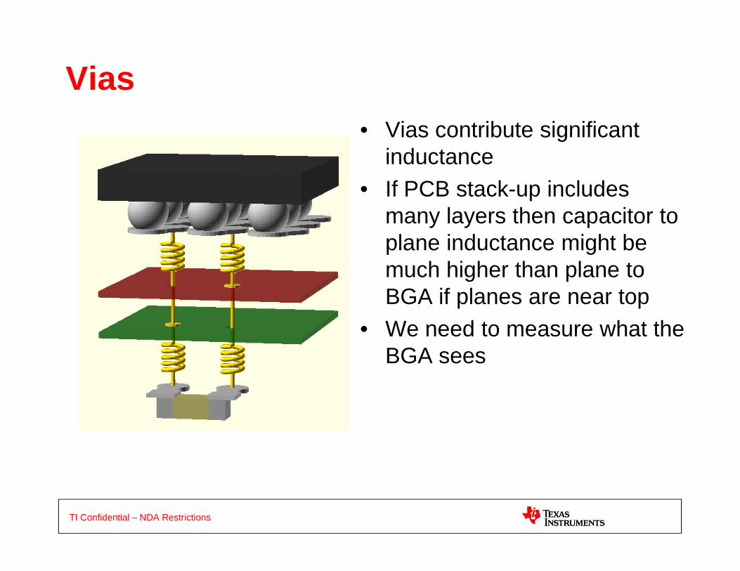
Vias• Vias contribute significant
inductance• If PCB stack-up includes
many layers then capacitor to plane inductance might beplane inductance might be much higher than plane to BGA if planes are near topW d t h t th• We need to measure what the BGA sees
TI Confidential – NDA Restrictions

Equivalent circuit• Measuring across points A yields
completely wrong values due to many series inductors andVia
1 HVia1 H
BGA
many series inductors and resistances
• Measuring across points B yields completely wrong values due to
1nH 1nH
Traces/planes & VRM
V
VCC
many series inductors and resistances
• Measuring across points C yields only low frequency noise
Via2nH
Via2nH
V
GND
only low frequency noise components due to filter formed by capacitor and via inductorsDECAP
0.1uF
Points A
Points B
Points C
TI Confidential – NDA Restrictions
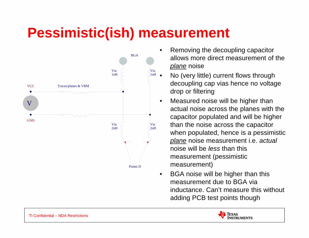
Pessimistic(ish) measurement
Via1nH
Via1nH
BGA• Removing the decoupling capacitor
allows more direct measurement of the plane noiseN ( littl ) t fl th h1nH 1nH
Traces/planes & VRM
V
VCC
• No (very little) current flows through decoupling cap vias hence no voltage drop or filtering
• Measured noise will be higher than
Via2nH
Via2nH
V
GND
gactual noise across the planes with the capacitor populated and will be higher than the noise across the capacitor when populated hence is a pessimisticwhen populated, hence is a pessimistic plane noise measurement i.e. actualnoise will be less than this measurement (pessimistic measurement)Points D measurement)
• BGA noise will be higher than this measurement due to BGA via inductance. Can’t measure this without
TI Confidential – NDA Restrictions
adding PCB test points though
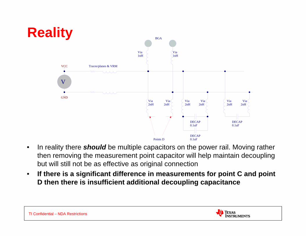
RealityBGA
Via1nH
Via1nH
Traces/planes & VRMVCC
Via Via
V
GNDVia Via Via Via
2nH 2nH 2nH 2nH
DECAP0.1uF
2nH 2nH
DECAP0.1uF
• In reality there should be multiple capacitors on the power rail. Moving rather then removing the measurement point capacitor will help maintain decoupling but will still not be as effective as original connection
Points DDECAP0.1uF
but will still not be as effective as original connection• If there is a significant difference in measurements for point C and point
D then there is insufficient additional decoupling capacitance
TI Confidential – NDA Restrictions
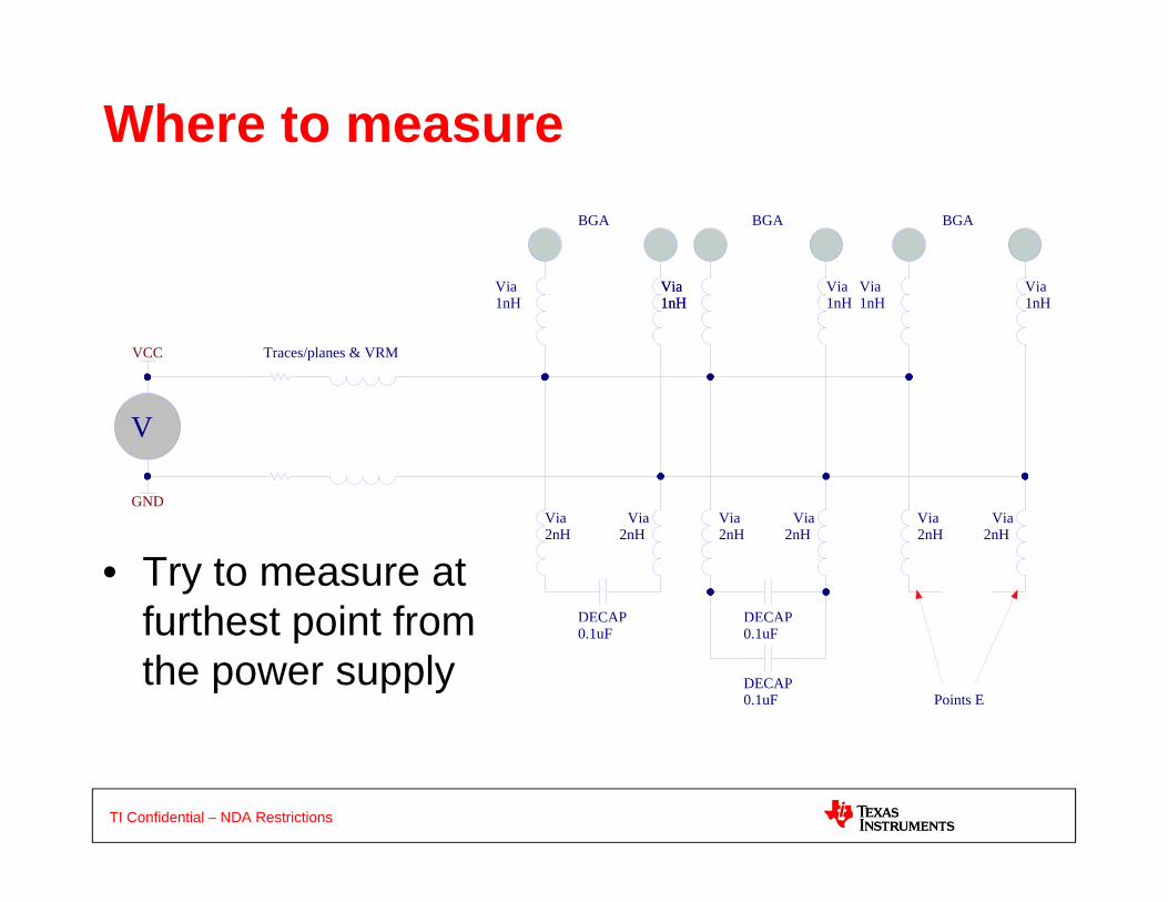
Where to measureBGA BGA BGA
Via1nH
Via1nH
Traces/planes & VRMVCC
Via1nH
Via1nH
Via1nH
Via1nH
V
GND
• Try to measure at furthest point from
Via2nH
Via2nH
Via2nH
Via2nH
DECAP
Via2nH
Via2nH
DECAPfurthest point from the power supply DECAP
0.1uF
C0.1uF
C0.1uF
Points E
TI Confidential – NDA Restrictions
Oscilloscope
• High speed scope required (250MHz + BW preferred)preferred)
• Correct oscilloscope configuration and usage is critical in analyzing high speed, high current, lowcritical in analyzing high speed, high current, low voltage power supply effectiveness
• Differential probes must be usedp• ‘Background’ noise measurements should be taken• High frequency components up to Fcutoff need toHigh frequency components up to Fcutoff need to
be considered. Fcutoff ~ 120MHz. BW limiting is OK above ~250MHz but do not limit much lower
TI Confidential – NDA Restrictions
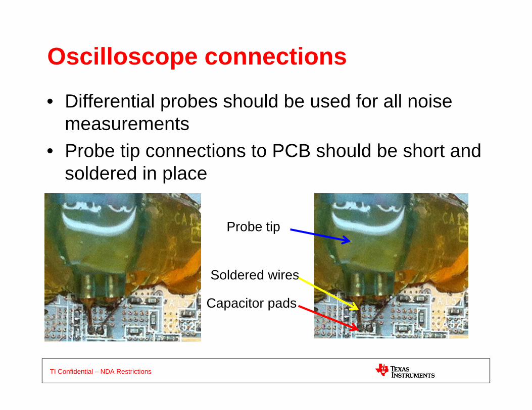
Oscilloscope connections
• Differential probes should be used for all noise measurementsmeasurements
• Probe tip connections to PCB should be short and soldered in placesoldered in place
Probe tipProbe tip
Soldered wires
Capacitor pads
TI Confidential – NDA Restrictions
Oscilloscope configuration
• Set the scope to infinite persistence• Set the scope to trigger on a low falling voltage• Set the scope to trigger on a low falling voltage• Put the scope on NORMAL trigger mode (not
AUTO and not SINGLE)AUTO and not SINGLE)• Add a measure function for the minimum,
maximum and average voltage If available alsomaximum and average voltage. If available also enable statistics
TI Confidential – NDA Restrictions
Baseline measurements
• Clean measurements require the amount of baseline noise to be understoodbaseline noise to be understood
• With the test system powered down short the capacitor test points together and measure thecapacitor test points together and measure the peak to peak, minimum and maximum voltage levels
• Make measurements at ~40ns, 1us and 1ms/div• If more than ~25mV then check the setup and
connections• If random spikes then check the setup and
TI Confidential – NDA Restrictions
connections
Supply noise measurements• Set scope to its maximum acquisition speed.
– On Tektronix scopes this is called “FastAcq”On Tektronix scopes this is called FastAcq• Power up the system and allow the application to start
running• Determine the nominal voltage level (zoom out vertically)• Set the channel offset to match the nominal voltage
Z i h ibl ti ll t 2/3 f th• Zoom in as much as possible vertically to cover ~2/3 of the vertical range
• Slowly adjust the trigger threshold as low as possible so that S o y adjus e gge es o d as o as poss b e so aonly occasional trigger events occur (every few seconds)
• Clear the display persistence image (keep persistence on)
TI Confidential – NDA Restrictions
• Leave running for as long as possible, at least few minutes

Results
• Long term noise = (max:max – min:min)– If statistics are enabled then use the maximum max and– If statistics are enabled then use the maximum max and
the minimum min values and not the mean values– Check these values with cursors on the persistence
image– Measurement we need is therefore the highest level
attained and the lowest level attainedattained and the lowest level attained
TI Confidential – NDA Restrictions
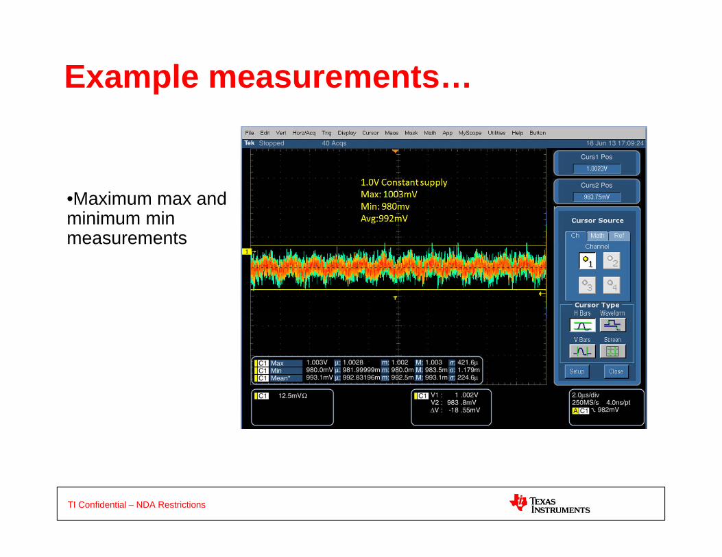
Example measurements…
•Maximum max and minimum min measurementsmeasurements
TI Confidential – NDA Restrictions
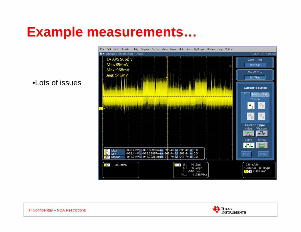
Example measurements…
•Lots of issues
TI Confidential – NDA Restrictions
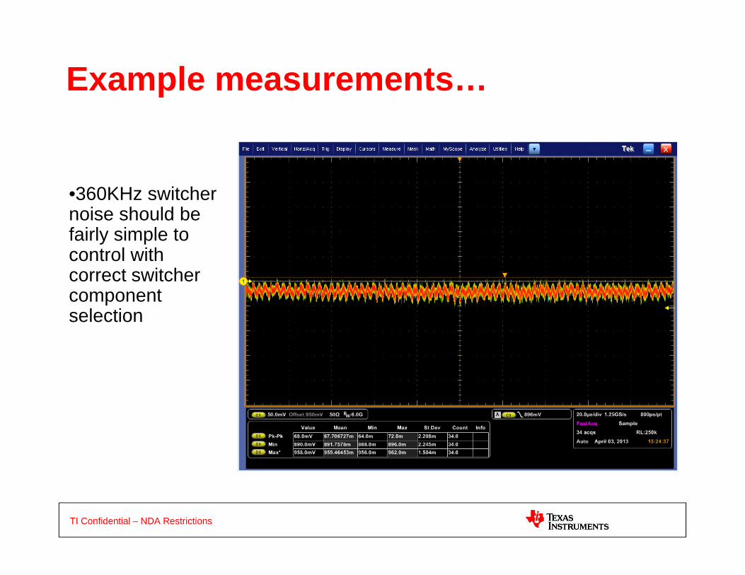
Example measurements…
•360KHz switcher noise should be fairly simple to control withcontrol with correct switcher component selection
TI Confidential – NDA Restrictions