power supply architectures for wireless systems with
TRANSCRIPT
18
Power Supply Architectures for Wireless Systems with Discontinuous Consumption
Jose Ignacio Garate and Jose Miguel de Diego Bilbao School of Engineering-University of the Basque Country/Trelec BTC S.L.L.
Spain
1. Introduction
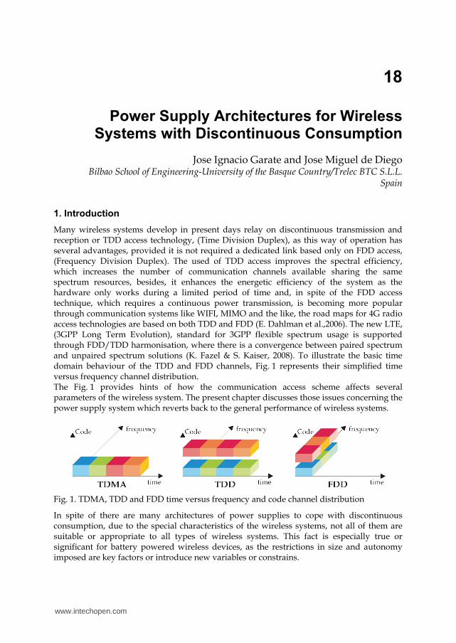
Many wireless systems develop in present days relay on discontinuous transmission and reception or TDD access technology, (Time Division Duplex), as this way of operation has several advantages, provided it is not required a dedicated link based only on FDD access, (Frequency Division Duplex). The used of TDD access improves the spectral efficiency, which increases the number of communication channels available sharing the same spectrum resources, besides, it enhances the energetic efficiency of the system as the hardware only works during a limited period of time and, in spite of the FDD access technique, which requires a continuous power transmission, is becoming more popular through communication systems like WIFI, MIMO and the like, the road maps for 4G radio access technologies are based on both TDD and FDD (E. Dahlman et al.,2006). The new LTE, (3GPP Long Term Evolution), standard for 3GPP flexible spectrum usage is supported through FDD/TDD harmonisation, where there is a convergence between paired spectrum and unpaired spectrum solutions (K. Fazel & S. Kaiser, 2008). To illustrate the basic time domain behaviour of the TDD and FDD channels, Fig. 1 represents their simplified time versus frequency channel distribution. The Fig. 1 provides hints of how the communication access scheme affects several parameters of the wireless system. The present chapter discusses those issues concerning the power supply system which reverts back to the general performance of wireless systems.
Fig. 1. TDMA, TDD and FDD time versus frequency and code channel distribution
In spite of there are many architectures of power supplies to cope with discontinuous consumption, due to the special characteristics of the wireless systems, not all of them are suitable or appropriate to all types of wireless systems. This fact is especially true or significant for battery powered wireless devices, as the restrictions in size and autonomy imposed are key factors or introduce new variables or constrains.
www.intechopen.com
Recent Advances in Wireless Communications and Networks
380
The research work that will be presented in this chapter is devoted to developing generic architectures of power supply systems for wireless systems, which possess the current consumption pattern of a discontinuous load. It also tries to answer, or at least eases to understand and face the design, development and production challenges related with the performance of wireless devices whenever they face with this type of current consumption.
2. Discontinuous consumption in wireless systems
As the discontinuous consumption concept is a generic topic, it requires a reference frame linked with wireless systems. This chapter considers two types of discontinuous consumption in wireless devices; a random one not directly involved in the communication process, for example, the activation of the backlights, the speaker, servos and the like, and a periodic one that will be addressed as discontinuous which is the subject of the research. This periodic consumption is linked with the access technology employ in the wireless system and leads to the transmission and reception time periods. In spite of such classification, it is interesting to highlight that almost all tasks performed by a wireless systems processor are controlled and previously programmed, therefore, the magnitude of the current consumption, demanded by a particular event, it is predefined.
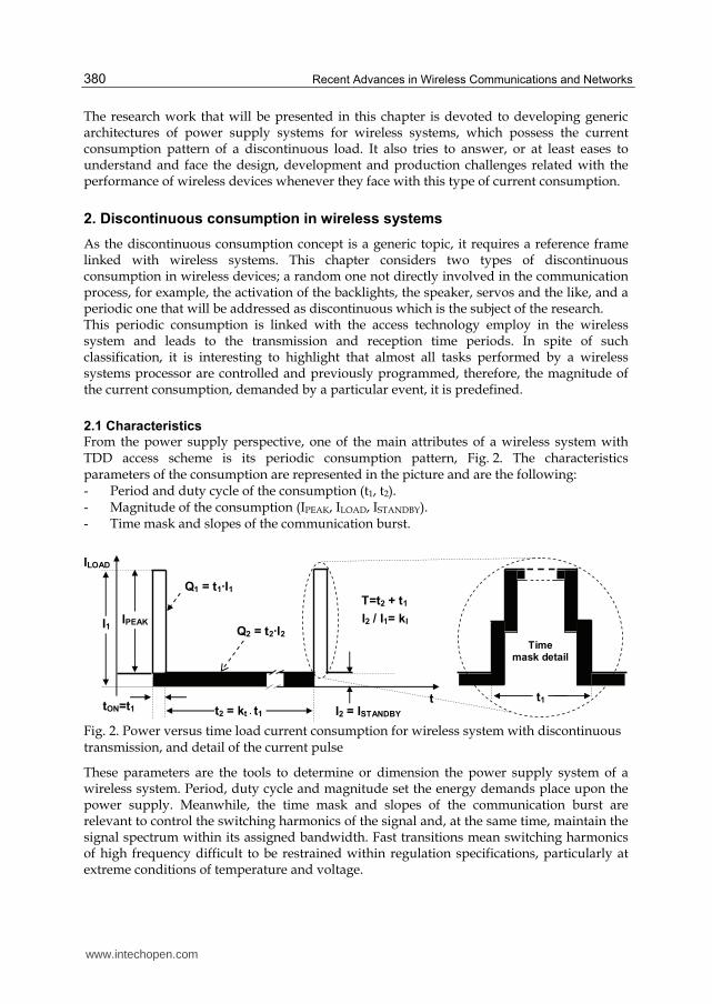
2.1 Characteristics
From the power supply perspective, one of the main attributes of a wireless system with TDD access scheme is its periodic consumption pattern, Fig. 2. The characteristics parameters of the consumption are represented in the picture and are the following: - Period and duty cycle of the consumption (t1, t2). - Magnitude of the consumption (IPEAK, ILOAD, ISTANDBY). - Time mask and slopes of the communication burst.
tON=t1 t
ILOAD
t2 = kt · t1 I2 = ISTANDBY
Q1 = t1·I1
Q2 = t2·I2 I2 / I1= kI IPEAK I1
t1
Time mask detail
T=t2 + t1
Fig. 2. Power versus time load current consumption for wireless system with discontinuous transmission, and detail of the current pulse
These parameters are the tools to determine or dimension the power supply system of a wireless system. Period, duty cycle and magnitude set the energy demands place upon the power supply. Meanwhile, the time mask and slopes of the communication burst are relevant to control the switching harmonics of the signal and, at the same time, maintain the signal spectrum within its assigned bandwidth. Fast transitions mean switching harmonics of high frequency difficult to be restrained within regulation specifications, particularly at extreme conditions of temperature and voltage.
www.intechopen.com
Power Supply Architectures for Wireless Systems with Discontinuous Consumption
381
2.2 Effects
The noticeable effects of discontinuous consumption in wireless systems are fluctuations
and drops in the supply voltage, applied to the terminals of the load, around the nominal
value; this fluctuation follows the consumption pattern. Voltage drop is ruled by the Ohm
law, but not only must be considered the distributed resistive component of electric path
between load and source, but also its reactive part. The resistive component conditions or
determines the magnitude of voltage drop, meanwhile; the reactive one defines the shape
and damping of consumption rise and fall slopes.
2.2.1 Voltage ripple
In wireless systems, the direct outcomes of voltage ripple are two; switching harmonics, and
voltage level out of operational ranges.
A) Switching harmonics
The frequency bandwidth available for a wireless system is a scarce resource and must be
optimized to allocate as many communication channels as possible. The TDD strategy to
achieve this goal is multiplex in time a number of channels at the same frequency within a
specific bandwidth. To make the communication systems work it is required that the
transmission is produced in a specific timing. Transceiver activation, on its assigned time
slot, is not produced instantaneously, which implies, before the information is received or
transmitted, that there are two periods of time for conditioning the signal. These two time
periods constitute the rise and fall ramp time. To this extent there are two situations to be
considered:
- If ramps are too fast implies high-frequency interferences, switching harmonics.
Switching harmonics reduce the amount of channel spectral density energy available
for communication, consequently, they degrade the link traffic capacity and its overall
performance, in other words, it means that could be set less communication links.
- If slopes are too slow, they widen the bandwidth and corrupt the spectral modulation
mask, which occupy the adjacent channel reducing the traffic maximum rate and the
sensitivity of adjacent receivers as their SINAD, (signal to noise ratio), is diminish.
B) Voltage ripple
The voltage level apply to the load varies between two values that correspond to minimum
a maximum load. It is likely that the voltage operative range of the wireless device is
exceeded in certain situations, particularly at extreme conditions of temperature.
Moreover, whenever wireless systems are battery powered, voltage drift increases as the
power source voltage varies, between maximum and minimum load, due to the battery
internal resistance. This is also applicable, to a certain extent, if a converter is placed
between the power source and the load, as voltage drift could set the converter out of its
regulation input voltage range.
2.2.2 Discontinuous current and electromagnetic compatibility
Seemingly, discontinuous consumption and voltage drops imply that the current is also variable. On the other hand, the discontinuous current drain from the power source has a direct impact on it, particularly for battery powered devices, which means energy losses in the internal battery resistance that are not uniform, as the load impedance presented varies
www.intechopen.com
Recent Advances in Wireless Communications and Networks
382
following the consumption pattern. Besides, existence of discontinuous current implies current flux through a wire, which induces magnetic fields on the power lines. There are three basic mechanisms or arrangements that produce magnetic fields; a signal track with a variable current, a current loop, and two parallel lines. The strength of magnetic fields varies with the level of current consumption, and their effects increase if there is any current loop involving the power lines that connect the source and load. These loops may produce interferences in any element of the wireless system, within or close to them. To make the phenomena challenging, usually, the frequency of magnetic field is a low- frequency one. It is known that a drawback of low frequency magnetic fields is their mechanism of attenuation. Magnetic fields require an absorptive shield, (ferrite), instead of the reflective one use for high frequency electric fields, which reduces its capability to shield them. Consequently, existence of magnetic fields implies side effects, in terms of the electromagnetic compatibility, EMC, of wireless systems, which should be avoided to fulfil the applicable regulation. Thus, design requires not only a careful routing and layout of power lines but also conditions the distribution of the wireless system architecture on PCB (M. I. Montrose, 1996).
3. Power supplies and discrete components for wireless systems
From the power supply perspective, once is stated that the classification of wireless systems starts with the type of access technology employ, which also defines if the consumption is continuous or periodic, for the power supply is the subject of this chapter, wireless systems will be sorted in two generic groups based on the type of power source they employ, in spite of inherit characteristics of portable wireless systems, like cellular terminals, impose certain restrictions over the power supply architecture and the devices it made of.
3.1 Types of power sources
Power sources are sensitive to the consumption patterns of wireless systems, but the power source itself conditions the architecture of both wireless device and power supply. Consequently, wireless systems are sorted in two groups; the first are systems directly connected to the power source, and the second is made of those that require a conditioning of the power source voltage and current.
3.1.1 Direct connection to power source
Apparently, the ideal scenario may be a power supply directly connected to the wireless systems or the load. As there is no electronic between source and load, the energy losses are reduced to those in the electric paths. This is true meanwhile the energy that the load drains from the battery is constant and correctly dimensioned to its internal resistance. This ideal situation is not such, as the energy drain is not always constant, the battery discharges over time and its capacity varies over the whole operational temperature range. Battery powered electronic devices such cellular terminals, PDAs, Ebook readers and the like are typical examples of wireless systems directly connected to the power source.
3.1.2 Voltage and current adapter
If the voltage and current levels of the source need to be conditioning, it is required a voltage converter between source and load. It does not matter if the power source is a solar
www.intechopen.com
Power Supply Architectures for Wireless Systems with Discontinuous Consumption
383
panel, a battery or the mains AC power lines, this fact will only affect the architecture of the voltage converter. There are tree generic alternatives: AC-DC isolated converter, DC-DC isolated converter and DC-DC converter (B. Sahu & G.A. Rincon-mora, 2004). Whenever AC power source is used, it is mandatory an AC-DC isolated converter, but the need of isolation between DC power source and the wireless systems is only a matter of electromagnetic compatibility standards, electrostatic discharges and security regulation.
3.2 Systems, component and devices for wireless power supply
Unless there is a wide range of components for power supplies and sources, the next lines summarize the requirements upon key components and devices of the power supply.
3.2.1 Battery
The main power source of portable or battery powered wireless systems is the battery cell itself (Saft, 2008). The battery could be primary or secondary, i.e., rechargeable or not rechargeable, respectively. From the point of view o the chapter, the battery equivalent circuit is made of its internal resistance, RIN. It use to be of low value and depends on the technology, tenths of milliohms for 1 Ahour capacity Ion-Lithium battery.
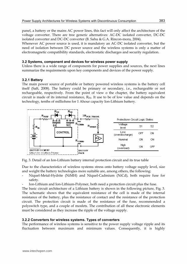
Fig. 3. Detail of an Ion-Lithium battery internal protection circuit and its true table
Due to the characteristics of wireless systems stress onto battery voltage supply level, size and weight the battery technologies more suitable are, among others, the following: - Niquel-Metal-Hydrite (NiMH) and Niquel-Cadmium (NiCd), both require fuse for
safety. - Ion-Lithium and Ion-Lithium-Polymer, both need a protection circuit plus the fuse. The basic circuit architecture of a Lithium battery is shown in the following picture, Fig. 3. The schematic shows that the equivalent resistance of the cell is made of the internal resistance of the battery, plus the resistance of contact and the resistance of the protection circuit. The protection circuit is made of the resistance of the fuse, recommended a polyswitch type, and a couple of mosfets. The contribution of all these electronic elements must be considered as they increase the ripple of the voltage supply.
3.2.2 Converters for wireless systems. Types of converters
The performance of wireless systems is sensitive to the power supply voltage ripple and its fluctuation between maximum and minimum values. Consequently, it is highly
www.intechopen.com
Recent Advances in Wireless Communications and Networks
384
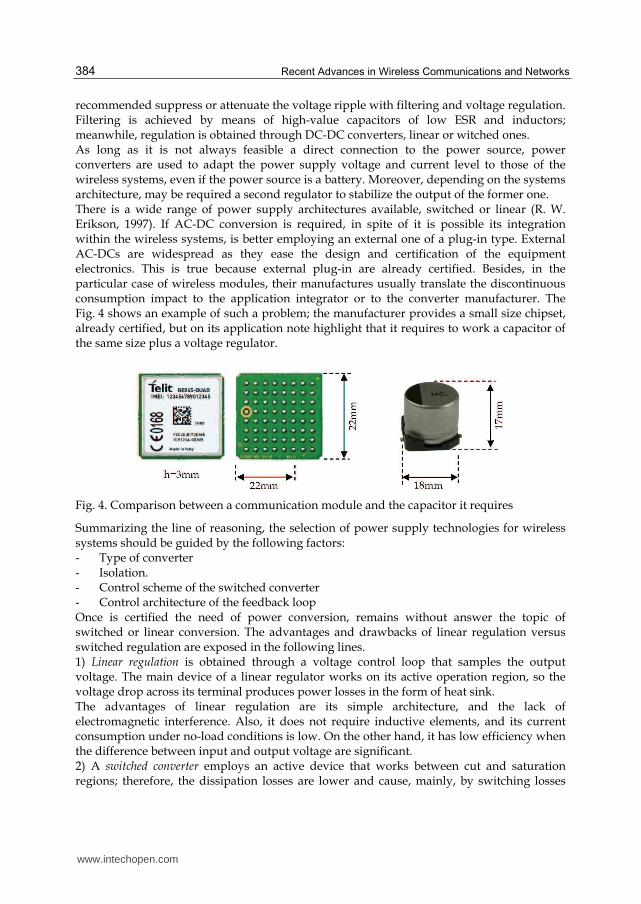
recommended suppress or attenuate the voltage ripple with filtering and voltage regulation. Filtering is achieved by means of high-value capacitors of low ESR and inductors; meanwhile, regulation is obtained through DC-DC converters, linear or witched ones. As long as it is not always feasible a direct connection to the power source, power converters are used to adapt the power supply voltage and current level to those of the wireless systems, even if the power source is a battery. Moreover, depending on the systems architecture, may be required a second regulator to stabilize the output of the former one. There is a wide range of power supply architectures available, switched or linear (R. W. Erikson, 1997). If AC-DC conversion is required, in spite of it is possible its integration within the wireless systems, is better employing an external one of a plug-in type. External AC-DCs are widespread as they ease the design and certification of the equipment electronics. This is true because external plug-in are already certified. Besides, in the particular case of wireless modules, their manufactures usually translate the discontinuous consumption impact to the application integrator or to the converter manufacturer. The Fig. 4 shows an example of such a problem; the manufacturer provides a small size chipset, already certified, but on its application note highlight that it requires to work a capacitor of the same size plus a voltage regulator.
Fig. 4. Comparison between a communication module and the capacitor it requires
Summarizing the line of reasoning, the selection of power supply technologies for wireless systems should be guided by the following factors: - Type of converter - Isolation. - Control scheme of the switched converter - Control architecture of the feedback loop Once is certified the need of power conversion, remains without answer the topic of switched or linear conversion. The advantages and drawbacks of linear regulation versus switched regulation are exposed in the following lines. 1) Linear regulation is obtained through a voltage control loop that samples the output voltage. The main device of a linear regulator works on its active operation region, so the voltage drop across its terminal produces power losses in the form of heat sink. The advantages of linear regulation are its simple architecture, and the lack of electromagnetic interference. Also, it does not require inductive elements, and its current consumption under no-load conditions is low. On the other hand, it has low efficiency when the difference between input and output voltage are significant. 2) A switched converter employs an active device that works between cut and saturation regions; therefore, the dissipation losses are lower and cause, mainly, by switching losses
www.intechopen.com
Power Supply Architectures for Wireless Systems with Discontinuous Consumption
385
and the voltage drop in the active device over cut and saturation. The power is delivered to the load through the energy store in an inductor, which charging cycle is a function of the energy demanded by the load. So, the energy drained from the source is used mostly to feeding the load, which reduces the power losses that are limited to those of the control circuit and the component leakages. Therefore, a performance analysis of switched converters shows that they provide a better balance between input and output voltages than the linear ones. They are, also, smaller and lighter than its linear counterparts for the same power rating, mainly because the isolation transformer is smaller. Furthermore, the size and value of the transformer or the switching inductance and the capacitors are reduced as the switching frequency is increased. Lower value capacitors contribute to reduce the voltage ripple, because it is possible used ceramic capacitors of low ESR, in the order of tenths milliohms or lower. On the other hand, a switched power supply introduces electromagnetic fields, radiated and conducted, that make the technical requirements restrictive, as the complexity of electronic design increases. Switched regulators are, also, more complex to design due to they require a higher number of discrete components, which reduces the electronic liability. Moreover, switched converter has another issue that must be bear in mind for green design applications. As long as the current consumption is discontinuous, the load remains inactive for some periods of time; during those periods its current consumption may reach zero. Hence, switched converter has poor efficiency under no-load conditions as there is a quiescent current in the electronic of the power supply. For example, standard 12 V and 4 W commercial DC-DC have a quiescent current consumption between 30 and 50 mA. Unless solutions switched regulation based may appear the most suitable, many manufactures employ linear regulation, especially when; there is available a power source with voltage levels close to those required by the wireless system, and size it is not a restriction. Doing so it is avoided EM fields, which increase cost and technical requirements.
3.2.3 Capacitors
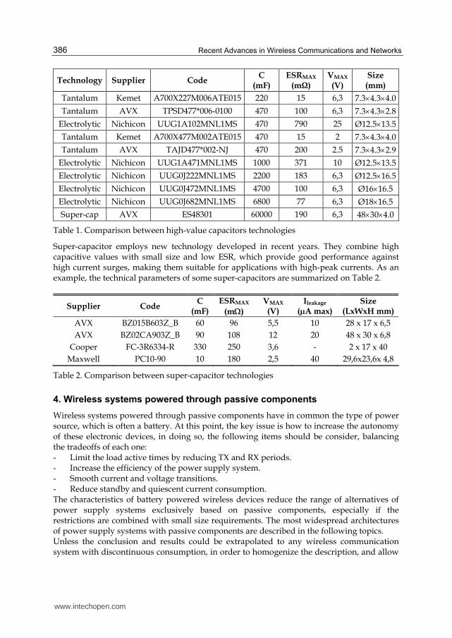
Power supply of wireless systems employs capacitors to store energy and filtering. The challenges to face are finding capacitors of high value, small size and low ESR that withstand the voltage levels applied to the electronics. Sometimes, the equipment size does not allow the use of high-value capacitors; the alternative is employ capacitors of hundred microfarads that only help to smooth voltage transitions. This is the case of GSM cellular terminals that when transmitting at maximum power, the peak current consumption may reach 3 A. Furthermore, capacitor ESR produces load voltage ripple, and its leakage resistance introduces a continuous discharge of the battery. For example, an standard tantalum capacitor, AVX model TPCL106M006#4000, has 10 µF nominal capacitance and ESR of 4000 mΩ. An electrolytic capacitor provides higher capacitance value on a bigger size and with more ESR. On the other hand, a ceramic one has small size and low ESR, but there are not feasible for high capacitance. Table 1 highlights the differences between technologies for the same capacitance value. Then the main limiting factors of capacitors are their ESR and size. The Table 1 provides a comparison between different types of capacitors. High value capacitors are intended to be used in the equipment, close to the load. To reduce the impact of the size it is possible; redistribute several capacitors in parallel, or use the technology of super-capacitors.
www.intechopen.com
Recent Advances in Wireless Communications and Networks
386
Technology Supplier Code C
(mF) ESRMAX
(mΩ) VMAX (V)
Size (mm)
Tantalum Kemet A700X227M006ATE015 220 15 6,3 7.3×4.3×4.0
Tantalum AVX TPSD477*006-0100 470 100 6,3 7.3×4.3×2.8
Electrolytic Nichicon UUG1A102MNL1MS 470 790 25 Ø12.5×13.5
Tantalum Kemet A700X477M002ATE015 470 15 2 7.3×4.3×4.0
Tantalum AVX TAJD477*002-NJ 470 200 2.5 7.3×4.3×2.9
Electrolytic Nichicon UUG1A471MNL1MS 1000 371 10 Ø12.5×13.5
Electrolytic Nichicon UUG0J222MNL1MS 2200 183 6,3 Ø12.5×16.5
Electrolytic Nichicon UUG0J472MNL1MS 4700 100 6,3 Ø16×16.5
Electrolytic Nichicon UUG0J682MNL1MS 6800 77 6,3 Ø18×16.5
Super-cap AVX ES48301 60000 190 6,3 48×30×4.0
Table 1. Comparison between high-value capacitors technologies
Super-capacitor employs new technology developed in recent years. They combine high capacitive values with small size and low ESR, which provide good performance against high current surges, making them suitable for applications with high-peak currents. As an example, the technical parameters of some super-capacitors are summarized on Table 2.
Supplier Code C
(mF)ESRMAX
(mΩ) VMAX (V)
Ileakage (µA max)
Size (LxWxH mm)
AVX BZ015B603Z_B 60 96 5,5 10 28 x 17 x 6,5
AVX BZ02CA903Z_B 90 108 12 20 48 x 30 x 6,8
Cooper FC-3R6334-R 330 250 3,6 - 2 x 17 x 40
Maxwell PC10-90 10 180 2,5 40 29,6x23,6x 4,8
Table 2. Comparison between super-capacitor technologies
4. Wireless systems powered through passive components
Wireless systems powered through passive components have in common the type of power source, which is often a battery. At this point, the key issue is how to increase the autonomy of these electronic devices, in doing so, the following items should be consider, balancing the tradeoffs of each one: - Limit the load active times by reducing TX and RX periods. - Increase the efficiency of the power supply system. - Smooth current and voltage transitions. - Reduce standby and quiescent current consumption. The characteristics of battery powered wireless devices reduce the range of alternatives of power supply systems exclusively based on passive components, especially if the restrictions are combined with small size requirements. The most widespread architectures of power supply systems with passive components are described in the following topics. Unless the conclusion and results could be extrapolated to any wireless communication system with discontinuous consumption, in order to homogenize the description, and allow
www.intechopen.com
Power Supply Architectures for Wireless Systems with Discontinuous Consumption
387
the comparison of different architectures, the reference wireless communication system is a GSM cellular terminal that transmits and receives only in one time slot. In this framework, the characteristics parameters of the terminal are the following: - Frequency of the GSM pulse = 216 Hz. - Transmission time, tON = 1/8 of the period, or time slot that last 578 µs. - Maximum current peak, ILOAD, 2 A for a nominal 3,6 V Ion-Lithium battery. - Standby current consumption, ISTANDBY 20 mA @ 3,6 V. - Mean current consumption, IMEAN, equals to 2 A · 1/8 + 0,02 A · 7/8=267,5 mA @ 3,6 V,
Ec. 1.
( )T
tTI
T
tII ON
STANDBYON
LOADMEAN−⋅+⋅= (1)
4.1 Direct connection
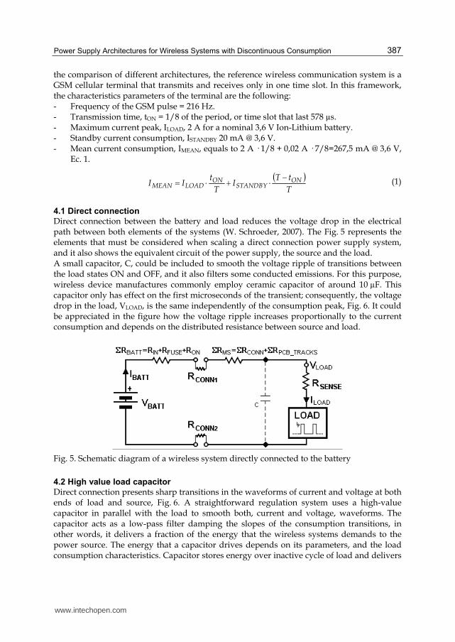
Direct connection between the battery and load reduces the voltage drop in the electrical path between both elements of the systems (W. Schroeder, 2007). The Fig. 5 represents the elements that must be considered when scaling a direct connection power supply system, and it also shows the equivalent circuit of the power supply, the source and the load. A small capacitor, C, could be included to smooth the voltage ripple of transitions between the load states ON and OFF, and it also filters some conducted emissions. For this purpose, wireless device manufactures commonly employ ceramic capacitor of around 10 µF. This capacitor only has effect on the first microseconds of the transient; consequently, the voltage drop in the load, VLOAD, is the same independently of the consumption peak, Fig. 6. It could be appreciated in the figure how the voltage ripple increases proportionally to the current consumption and depends on the distributed resistance between source and load.
Fig. 5. Schematic diagram of a wireless system directly connected to the battery
4.2 High value load capacitor
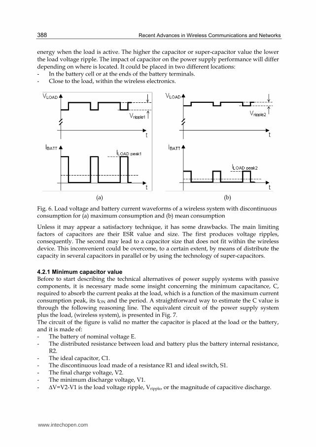
Direct connection presents sharp transitions in the waveforms of current and voltage at both ends of load and source, Fig. 6. A straightforward regulation system uses a high-value capacitor in parallel with the load to smooth both, current and voltage, waveforms. The capacitor acts as a low-pass filter damping the slopes of the consumption transitions, in other words, it delivers a fraction of the energy that the wireless systems demands to the power source. The energy that a capacitor drives depends on its parameters, and the load consumption characteristics. Capacitor stores energy over inactive cycle of load and delivers
www.intechopen.com
Recent Advances in Wireless Communications and Networks
388
energy when the load is active. The higher the capacitor or super-capacitor value the lower the load voltage ripple. The impact of capacitor on the power supply performance will differ depending on where is located. It could be placed in two different locations: - In the battery cell or at the ends of the battery terminals. - Close to the load, within the wireless electronics.
(a) (b)
Fig. 6. Load voltage and battery current waveforms of a wireless system with discontinuous consumption for (a) maximum consumption and (b) mean consumption
Unless it may appear a satisfactory technique, it has some drawbacks. The main limiting factors of capacitors are their ESR value and size. The first produces voltage ripples, consequently. The second may lead to a capacitor size that does not fit within the wireless device. This inconvenient could be overcome, to a certain extent, by means of distribute the capacity in several capacitors in parallel or by using the technology of super-capacitors.
4.2.1 Minimum capacitor value
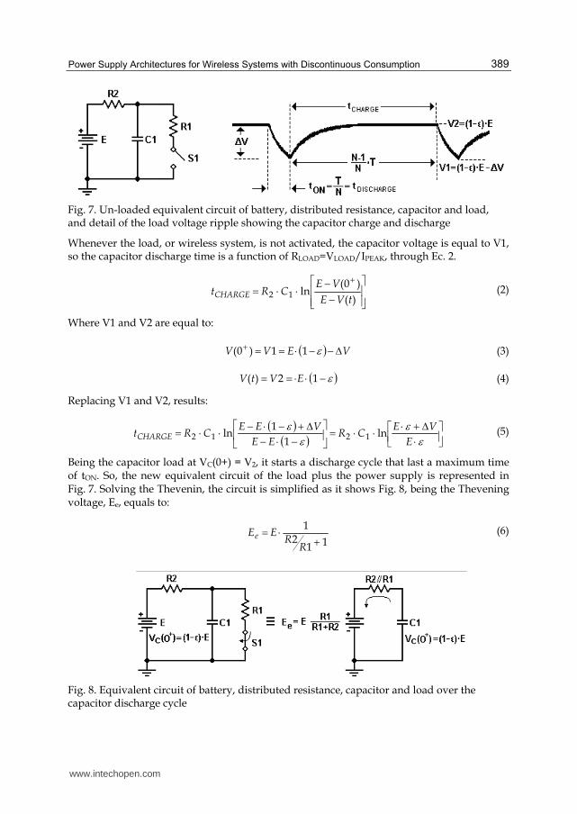
Before to start describing the technical alternatives of power supply systems with passive components, it is necessary made some insight concerning the minimum capacitance, C, required to absorb the current peaks at the load, which is a function of the maximum current consumption peak, its tON and the period. A straightforward way to estimate the C value is through the following reasoning line. The equivalent circuit of the power supply system plus the load, (wireless system), is presented in Fig. 7. The circuit of the figure is valid no matter the capacitor is placed at the load or the battery, and it is made of: - The battery of nominal voltage E. - The distributed resistance between load and battery plus the battery internal resistance,
R2. - The ideal capacitor, C1. - The discontinuous load made of a resistance R1 and ideal switch, S1. - The final charge voltage, V2. - The minimum discharge voltage, V1. - ΔV=V2-V1 is the load voltage ripple, Vripple, or the magnitude of capacitive discharge.
www.intechopen.com
Power Supply Architectures for Wireless Systems with Discontinuous Consumption
389
Fig. 7. Un-loaded equivalent circuit of battery, distributed resistance, capacitor and load, and detail of the load voltage ripple showing the capacitor charge and discharge
Whenever the load, or wireless system, is not activated, the capacitor voltage is equal to V1, so the capacitor discharge time is a function of RLOAD=VLOAD/IPEAK, through Ec. 2.
⎥⎥⎦⎤
⎢⎢⎣⎡
−−⋅⋅= +
)(
)0(ln12
tVE
VECRtCHARGE (2)
Where V1 and V2 are equal to:
( ) VEVV Δ−−⋅==+ ε11)0( (3)
( )ε−⋅⋅== 12)( EVtV (4)
Replacing V1 and V2, results:
( )( ) ⎥⎦⎤⎢⎣
⎡⋅Δ+⋅⋅⋅=⎥⎦
⎤⎢⎣⎡
−⋅−Δ+−⋅−⋅⋅= ε
εε
εE
VECR
EE
VEECRtCHARGE ln
1
1ln 1212
(5)
Being the capacitor load at VC(0+) = V2, it starts a discharge cycle that last a maximum time of tON. So, the new equivalent circuit of the load plus the power supply is represented in Fig. 7. Solving the Thevenin, the circuit is simplified as it shows Fig. 8, being the Thevening voltage, Ee, equals to:
11
2
1
+⋅=R
REEe
(6)
Fig. 8. Equivalent circuit of battery, distributed resistance, capacitor and load over the capacitor discharge cycle
www.intechopen.com
Recent Advances in Wireless Communications and Networks
390
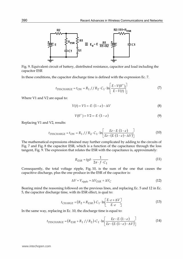
Fig. 9. Equivalent circuit of battery, distributed resistance, capacitor and load including the capacitor ESR
In these conditions, the capacitor discharge time is defined with the expression Ec. 7.
⎥⎥⎦⎤
⎢⎢⎣⎡
−−⋅⋅== +
)(
)0(ln// 121
tVE
VECRRtt ONDISCHARGE
(7)
Where V1 and V2 are equal to:
( ) VEVtV Δ−−⋅⋅== ε11)( (8)
( )ε−⋅⋅==+ 12)0( EVV (9)
Replacing V1 and V2, results:
( )( )( )⎥⎦⎤⎢⎣
⎡Δ−−⋅−
−⋅−⋅⋅==VEEe
EEeCRRtt ONDISCHARGE ε
ε1
1ln// 121
(10)
The mathematical expressions obtained may further complicated by adding to the circuits of Fig. 7 and Fig. 8 the capacitor ESR, which is a function of the capacitance through the loss tangent, Fig. 9. The expression that relates the ESR with the capacitance is, approximately:
12
1
CftgRESR ⋅⋅⋅= πδ (11)
Consequently, the total voltage ripple, Fig. 10, is the sum of the one that causes the capacitive discharge, plus the one produce in the ESR of the capacitor is:
CESRripple VVVV Δ+Δ==Δ (12)
Bearing mind the reasoning followed on the previous lines, and replacing Ec. 5 and 12 in Ec. 5, the capacitor discharge time, with its ESR effect, is qual to:
( ) ⎥⎦⎤⎢⎣
⎡⋅Δ+⋅⋅⋅+= ε
εE
VECRRt ESRCHARGE ln12
(13)
In the same way, replacing in Ec. 10, the discharge time is equal to:
( ) ( )( )( )⎥⎦⎤⎢⎣
⎡Δ−−⋅−
−⋅−⋅⋅+=VEEe
EEeCRRRt ESRDISCHARGE ε
ε1
1ln// 121
(14)
www.intechopen.com
Power Supply Architectures for Wireless Systems with Discontinuous Consumption
391
This lasts equations estimate the capacitance as a function of the targeted voltage ripple.
Fig. 10. Ideal waveform detail of the load voltage ripple showing the capacitor charge and discharge, and including the capacitor ESR contribution
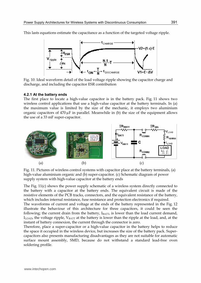
4.2.1 At the battery ends The first place to locate a high-value capacitor is in the battery pack. Fig. 11 shows two wireless control applications that use a high-value capacitor at the battery terminals. In (a) the maximum value is limited by the size of the mechanic, it employs two aluminium organic capacitors of 470 μF in parallel. Meanwhile in (b) the size of the equipment allows the use of a 33 mF super-capacitor.
(a) (b) (c)
Fig. 11. Pictures of wireless control systems with capacitor place at the battery terminals, (a) high-value aluminium organic and (b) super-capacitor. (c) Schematic diagram of power supply system with high-value capacitor at the battery ends
The Fig. 11(c) shows the power supply schematic of a wireless system directly connected to the battery with a capacitor at the battery ends. The equivalent circuit is made of the resistive elements of the PCB tracks, connectors, and the equivalent resistance of the battery, which includes internal resistance, fuse resistance and protection electronics if required. The waveforms of current and voltage at the ends of the battery represented in the Fig. 12 illustrate the behaviour of this architecture for three capacitors, it could be seen the following; the current drain from the battery, IBATT, is lower than the load current demand, ILOAD, the voltage ripple, VBATT at the battery is lower than the ripple at the load, and, at the instant of battery connexion, the current through the connector is zero. Therefore, place a super-capacitor or a high-value capacitor in the battery helps to reduce the space it occupied in the wireless device, but increases the size of the battery pack. Super-capacitors also presents manufacturing disadvantages as they are not suitable for automatic surface mount assembly, SMD, because do not withstand a standard lead-free oven soldering profile.
www.intechopen.com
Recent Advances in Wireless Communications and Networks
392
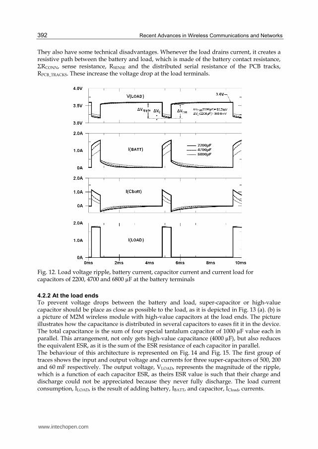
They also have some technical disadvantages. Whenever the load drains current, it creates a resistive path between the battery and load, which is made of the battery contact resistance, ΣRCONN, sense resistance, RSENSE and the distributed serial resistance of the PCB tracks, RPCB_TRACKS. These increase the voltage drop at the load terminals.
Fig. 12. Load voltage ripple, battery current, capacitor current and current load for capacitors of 2200, 4700 and 6800 µF at the battery terminals
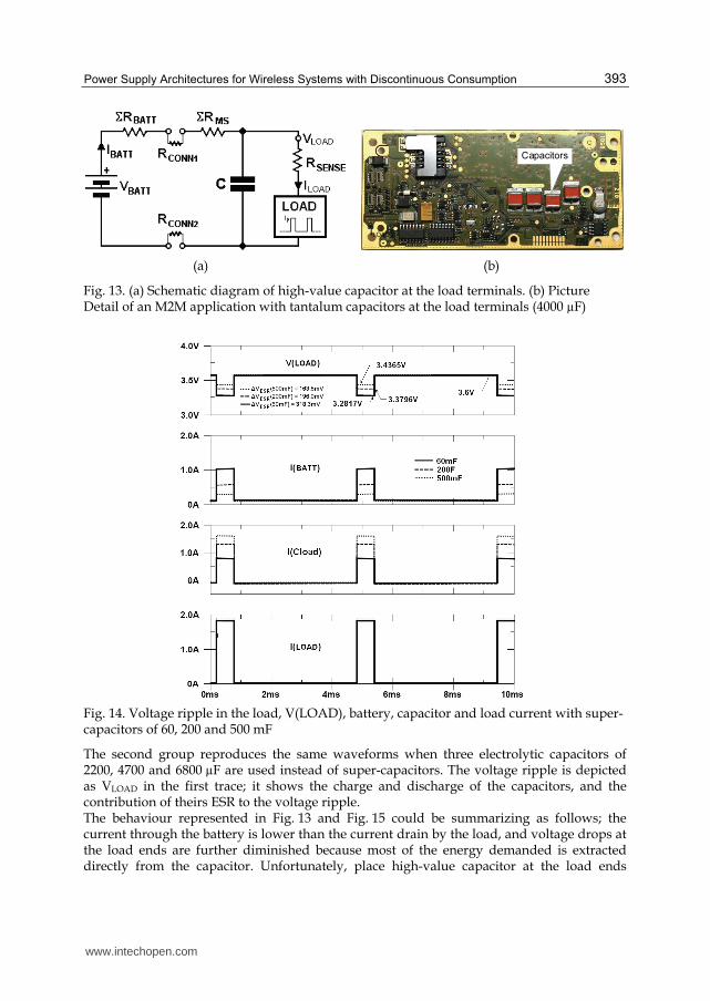
4.2.2 At the load ends To prevent voltage drops between the battery and load, super-capacitor or high-value capacitor should be place as close as possible to the load, as it is depicted in Fig. 13 (a). (b) is a picture of M2M wireless module with high-value capacitors at the load ends. The picture illustrates how the capacitance is distributed in several capacitors to eases fit it in the device. The total capacitance is the sum of four special tantalum capacitor of 1000 µF value each in parallel. This arrangement, not only gets high-value capacitance (4000 µF), but also reduces the equivalent ESR, as it is the sum of the ESR resistance of each capacitor in parallel. The behaviour of this architecture is represented on Fig. 14 and Fig. 15. The first group of traces shows the input and output voltage and currents for three super-capacitors of 500, 200 and 60 mF respectively. The output voltage, VLOAD, represents the magnitude of the ripple, which is a function of each capacitor ESR, as theirs ESR value is such that their charge and discharge could not be appreciated because they never fully discharge. The load current consumption, ILOAD, is the result of adding battery, IBATT, and capacitor, ICload, currents.
www.intechopen.com
Power Supply Architectures for Wireless Systems with Discontinuous Consumption
393
ILOAD
Capacitors
(a) (b)
Fig. 13. (a) Schematic diagram of high-value capacitor at the load terminals. (b) Picture Detail of an M2M application with tantalum capacitors at the load terminals (4000 µF)
Fig. 14. Voltage ripple in the load, V(LOAD), battery, capacitor and load current with super-capacitors of 60, 200 and 500 mF
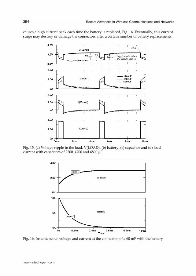
The second group reproduces the same waveforms when three electrolytic capacitors of 2200, 4700 and 6800 µF are used instead of super-capacitors. The voltage ripple is depicted as VLOAD in the first trace; it shows the charge and discharge of the capacitors, and the contribution of theirs ESR to the voltage ripple. The behaviour represented in Fig. 13 and Fig. 15 could be summarizing as follows; the current through the battery is lower than the current drain by the load, and voltage drops at the load ends are further diminished because most of the energy demanded is extracted directly from the capacitor. Unfortunately, place high-value capacitor at the load ends
www.intechopen.com
Recent Advances in Wireless Communications and Networks
394
causes a high current peak each time the battery is replaced, Fig. 16. Eventually, this current surge may destroy or damage the connectors after a certain number of battery replacements.
Fig. 15. (a) Voltage ripple in the load, V(LOAD), (b) battery, (c) capacitor and (d) load current with capacitors of 2200, 4700 and 6800 µF
Fig. 16. Instantaneous voltage and current at the connexion of a 60 mF with the battery
www.intechopen.com
Power Supply Architectures for Wireless Systems with Discontinuous Consumption
395
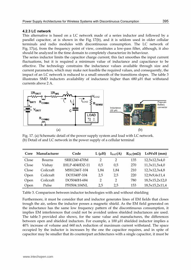
4.2.3 LC network
This alternative is based on a LC network made of a series inductor and followed by a parallel capacitor, at is shown in the Fig. 17(b), and it is seldom used in older cellular terminals and radio modules with discontinuous consumption. The LC network of Fig. 17(a), from the frequency point of view, constitutes a low-pass filter, although, it also should be analyzed in the time domain to completely characterize its behaviour. The series inductor limits the capacitor charge current; this fact smoothes the input current fluctuations, but it is required a minimum value of inductance and capacitance to be effective. The technology constrains the inductance values available through size and current parameters, which may make not feasible the required values, and consequently, the impact of an LC network is reduced to a small smooth of the transitions slopes. The table 3 illustrates SMD inductors availability of inductance higher than 680 µH that withstand currents above 2 A.
Inductance
(22 µH)
Pogo-pin
Battery
connector
(a) (b)
Fig. 17. (a) Schematic detail of the power supply system and load with LC network. (b) Detail of and LC network in the power supply of a cellular terminal
Core Manufacturer Code L (µH) ISAT(A) RDC(mΩ) LxWxH (mm)
Close Bourns SRR1240-470M 2 2 135 12,5x12,5x4,0
Close Vishay IHLP-4040DZ-11 0,5 0,5 270 11,3x11,5x4,0
Close Coilcraft MSS1246T-104 1,84 1,84 210 12,3x12,3x4,8
Open Coilcraft DO3340P-104 2,5 2,5 220 12,9x9,4x11,4
Open Coilcraft DO5040H-684 2 2 780 18,5x15,2x12,0
Open Pulse PF0504.104NL 2,5 2,5 153 18,5x15,2x11,4
Table 3. Comparison between inductor technologies with and without shielding
Furthermore, it must be consider that and inductor generates lines of EM fields that closes trough the air, unless the inductor posses a magnetic shield. As the EM field generated on the inductance has the same low frequency pattern of the discontinuous consumption, it implies EM interferences that could not be avoided unless shielded inductances are used. The table 3 provided also shows, for the same value and manufactures, the differences between open and shielded inductors. For example, a 100 µH shielded inductor implies a 40% increase of volume and 660 mA reduction of maximum current withstand. The space occupied by the inductor is increases by the one the capacitor requires, and in spite of capacitor may be smaller that its counterpart architectures with a single capacitor, it must be
www.intechopen.com
Recent Advances in Wireless Communications and Networks
396
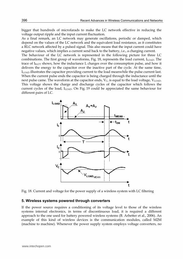
bigger that hundreds of microfarads to make the LC network effective in reducing the voltage output ripple and the input current fluctuation. As a final remark, an LC network may generate oscillations, periodic or damped, which depend on the values of the LC network and the equivalent load resistance, as it constitutes a RLC network affected by a pulsed signal. This also means that the input current could have negative values, which implies a current send back to the battery, i.e., a charging current. The behaviour of the LC network is represented in the following picture for three LC combinations. The first group of waveforms, Fig. 18, represents the load current, ILOAD. The trace of IBATT shows, how the inductance L charges over the consumption pulse, and how it delivers the energy to the capacitor over the inactive part of the cycle. At the same time, ILOAD illustrates the capacitor providing current to the load meanwhile the pulse current last. When the current pulse ends the capacitor is being charged through the inductance until the next pulse came. The waveform at the capacitor ends, VC, is equal to the load voltage, VLOAD. This voltage shows the charge and discharge cycles of the capacitor which follows the current cycles of the load, ILOAD. On Fig. 19 could be appreciated the same behaviour for different pairs of LC.
Fig. 18. Current and voltage for the power supply of a wireless system with LC filtering
5. Wireless systems powered through converters
If the power source requires a conditioning of its voltage level to those of the wireless systems internal electronics, in terms of discontinuous load, it is required a different approach to the one used for battery powered wireless systems (B. Arbetter et al., 2006). An example of this kind of wireless devices is the communication modules, called M2M (machine to machine). Whenever the power supply system employs voltage converters, no
www.intechopen.com
Power Supply Architectures for Wireless Systems with Discontinuous Consumption
397
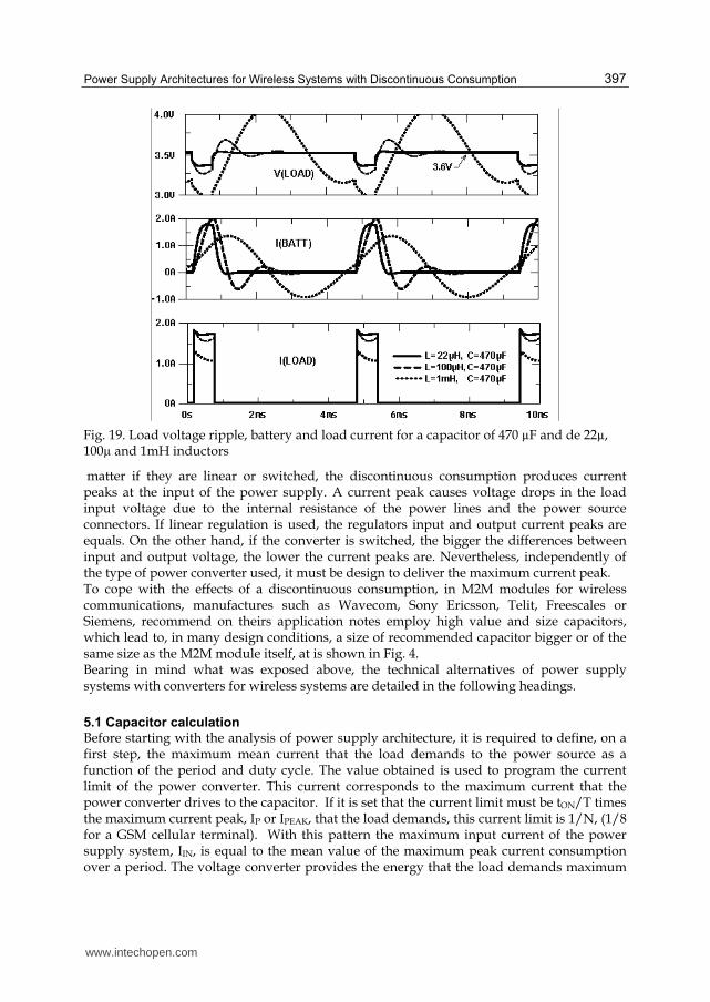
Fig. 19. Load voltage ripple, battery and load current for a capacitor of 470 µF and de 22µ, 100µ and 1mH inductors
matter if they are linear or switched, the discontinuous consumption produces current peaks at the input of the power supply. A current peak causes voltage drops in the load input voltage due to the internal resistance of the power lines and the power source connectors. If linear regulation is used, the regulators input and output current peaks are equals. On the other hand, if the converter is switched, the bigger the differences between input and output voltage, the lower the current peaks are. Nevertheless, independently of the type of power converter used, it must be design to deliver the maximum current peak. To cope with the effects of a discontinuous consumption, in M2M modules for wireless communications, manufactures such as Wavecom, Sony Ericsson, Telit, Freescales or Siemens, recommend on theirs application notes employ high value and size capacitors, which lead to, in many design conditions, a size of recommended capacitor bigger or of the same size as the M2M module itself, at is shown in Fig. 4. Bearing in mind what was exposed above, the technical alternatives of power supply systems with converters for wireless systems are detailed in the following headings.
5.1 Capacitor calculation Before starting with the analysis of power supply architecture, it is required to define, on a first step, the maximum mean current that the load demands to the power source as a function of the period and duty cycle. The value obtained is used to program the current limit of the power converter. This current corresponds to the maximum current that the power converter drives to the capacitor. If it is set that the current limit must be tON/T times the maximum current peak, IP or IPEAK, that the load demands, this current limit is 1/N, (1/8 for a GSM cellular terminal). With this pattern the maximum input current of the power supply system, IIN, is equal to the mean value of the maximum peak current consumption over a period. The voltage converter provides the energy that the load demands maximum
www.intechopen.com
Recent Advances in Wireless Communications and Networks
398
consumption. Consequently, unless the maximum mean current will never overcome, IIN follows the load consumption fluctuations, at it is described in the following expression:
/T t I I ONPEAKIN ⋅= (15)
Where, - tON o tdischarge is the duty cycle of consumption, equal to the capacitive discharge time. - T is the consumption period. - IPEAK is the maximum peak consumption over a period. Thus, the required capacitance is obtained through the following reasoning. Being the current through the capacitor:
dtdVCI /⋅= (16)
And considering that, on an ideal situation, the charge and discharge of a capacitor is lineal. This is feasible as the maximum drive current of the voltage converted is limited to a fixed value. Thus, doing the differential voltage equal to the voltage increment, Vripple, and the differential time equal to the time increment, tON, the current is equal:
tVCI ΔΔ⋅= / (17)
Solving for the capacitance value, and considering that the voltage ripple ΔVC, for an ideal capacitor, has only a capacitive discharging contribution, the capacitance results:
CON VtIC Δ⋅= / (18)
For example, if the mean load current is 250 mA, for a maximum peak current of 2 A, and a period time of 4,64 ms, the capacitance value, (without including the effect of its ESR), for a maximum load voltage ripple of 0,4 V, is:
µF3600 V0,4 / µs 580 · A 0,250 ≅= C (19)
5.2 Constant input current power supply Once it is stated that a high-value capacitor smoothes current and voltage transitions and reduces its magnitude, but does not maintain constant the voltage excursion around the nominal voltage values of the power source. The first improvement could be add a voltage regulator to the capacitor, Fig. 20. The power supply system of Fig. 20 is made of a lineal or switched regulator with a fixed current limit, plus a high-value capacitor close to the wireless system load. The Fig. 20 includes the connector and power lines resistance, RIN. Following this equivalent resistance it is placed the current limited voltage regulator. The current limit of the regulator must be adjusted, approximately, to the maximum peak current averaged by N for a period. For an EGSM cellular terminal, this current is equal to the number of time slots used for transmission, IPEAK/8. With this power supply architecture the input current, IIN, always has a value close to the average current consumption. At any time, the regulator is able to provide the maximum power that the wireless system load may demand. For example, on a M2M GSM module, the input current, IIN, varies following the consumption fluctuations, and never overcomes the maximum average consumption, IPEAK/8. The RSENSE resistance is used to measure the current that the capacitor drains or supplies, and, at the same time, limits the maximum current that the converter could provide. If the wireless systems
www.intechopen.com
Power Supply Architectures for Wireless Systems with Discontinuous Consumption
399
requires electronics to monitoring o control the TX power it could be done by means of a current sensor, RSENSE, this element increase the voltage drop and must be consider. Unless linear conversion is an option, a switched regulator is a better solution, meanwhile the electromagnetic fields generated are under control. Linear regulation reduces the power efficiency of the supply system as the input voltage of the power source may vary over a wide range of values. As a design rule, whenever the magnitude difference between input and output voltage are not relevant a linear regulator could be used.
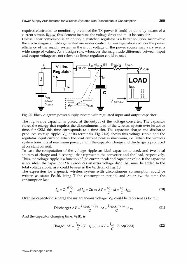
Fig. 20. Block diagram power supply system with regulated input and output capacitor
The high-value capacitor is placed at the output of the voltage converter. The capacitor stores the energy that requires the discontinuous load of the wireless system over its active time, for GSM this time corresponds to a time slot. The capacitor charge and discharge produces voltage ripple, VC, at its terminals. Fig. 21(a) shows this voltage ripple and the regulator input current, when the load current peak is maximum, i.e., when the wireless system transmits at maximum power, and if the capacitor charge and discharge is produced at constant current. To ease the computation of the voltage ripple an ideal capacitor is used, and two ideal sources of charge and discharge, that represents the converter and the load, respectively. Thus, the voltage ripple is a function of the current peak and capacitor value. If the capacitor is not ideal, the capacitor ESR introduces an extra voltage drop that must be added to the total voltage ripple, as it could be seen in the VC detail of Fig. 10. The expression for a generic wireless system with discontinuous consumption could be written as states Ec. 20, being T the consumption period, and Δt or tON the time the consumption last.
ON
CCC
CC t
C
It
C
IVCteIsi
dt
dVCI ⋅=Δ⋅=Δ⇒=⋅= , (20)
Over the capacitor discharge the instantaneous voltage, VC, could be represent as Ec. 21:
ON
INPEAKINPEAK tC
IIt
C
IIV ⋅−=Δ⋅−=Δ :Discharge (21)
And the capacitor charging time, VC(t), is:
( ) )(7 :Charge GSMtC
IVtT
C
IV IN
ONIN Δ⋅⋅=Δ⇒−⋅=Δ (22)
www.intechopen.com
Recent Advances in Wireless Communications and Networks
400
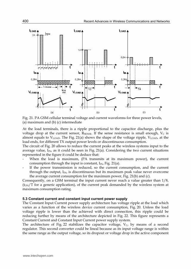
Fig. 21. PA GSM cellular terminal voltage and current waveforms for three power levels, (a) maximum and (b) (c) intermediate
At the load terminals, there is a ripple proportional to the capacitor discharge, plus the voltage drop at the current sensor, RSENSE. If the sense resistance is small enough, VC is almost equals to VLOAD. The Fig. 21(a) shows the shape of the voltage ripple, VLOAD, at the load ends, for different TX output power levels or discontinuous consumption. The circuit of Fig. 20 allows to reduce the current peaks at the wireless systems input to the average value, IIN, as it could be seen in Fig. 21(a). Considering the two current situations represented in the figure it could be deduce that: - When the load is maximum, (PA transmits at its maximum power), the current
consumption through the input is constant, IIN, Fig. 21(a). - If the power transmission is reduced, so the current consumption, and the current
through the output, IIN, is discontinuous but its maximum peak value never overcome the average current consumption for the maximum power, Fig. 21(b) and (c).
Consequently, on a GSM terminal the input current never reach a value greater than 1/8, (tON/T for a generic application), of the current peak demanded by the wireless system at maximum consumption rating.
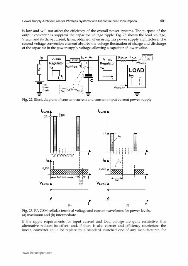
5.3 Constant current and constant input current power supply The Constant Input Current power supply architecture has voltage ripple at the load which varies as a function of the wireless device current consumption, Fig. 20. Unless the load voltage ripple is lower than the achieved with direct connection, this ripple could be reducing further by means of the architecture depicted in Fig. 22. This figure represents a Constant Current and Constant Input Current power supply system. The architecture of Fig. 22 stabilizes the capacitor voltage, VC, by means of a second regulator. This second converter could be lineal because as its input voltage range is within the same range as the output voltage, so its dropout or voltage drop in the active component
www.intechopen.com
Power Supply Architectures for Wireless Systems with Discontinuous Consumption
401
is low and will not affect the efficiency of the overall power systems. The purpose of the output converter is suppress the capacitor voltage ripple. Fig. 23 shows the load voltage, VLOAD, and its drive current, ILOAD, obtained when using this power supply architecture. The second voltage conversion element absorbs the voltage fluctuation of charge and discharge of the capacitor in the power supply voltage, allowing a capacitor of lower value.
Fig. 22. Block diagram of constant current and constant input current power supply
Fig. 23. PA GSM cellular terminal voltage and current waveforms for power levels, (a) maximum and (b) intermediate
If the ripple requirements for input current and load voltage are quite restrictive, this alternative reduces its effects and, if there is also current and efficiency restrictions the linear, converter could be replace by a standard switched one of any manufacturer, for
www.intechopen.com
Recent Advances in Wireless Communications and Networks
402
example, a MAX1678. This device has some advantage as it is specially design for GSM and UMTS, with the remark that is only efficiency in boost mode.
5.4 Summary
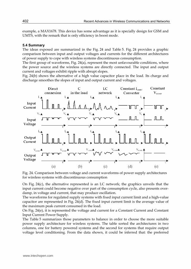
The ideas exposed are summarized in the Fig. 24 and Table 5. Fig. 24 provides a graphic comparison between input and output voltages and currents for the different architectures of power supply to cope with wireless systems discontinuous consumption. The first group of waveforms, Fig. 24(a), represent the most unfavourable conditions, where the power source and the wireless systems are directly connected. The input and output current and voltages exhibit ripple with abrupt slopes. Fig. 24(b) shows the alternative of a high value capacitor place in the load. Its charge and discharge smoothes the slopes of input and output current and voltages.
Fig. 24. Comparison between voltage and current waveforms of power supply architectures for wireless systems with discontinuous consumption
On Fig. 24(c), the alternative represented is an LC network; the graphics unveils that the input current could become negative over part of the consumption cycle, also presents over-damp, in voltage and current, that may produce oscillation. The waveforms for regulated supply systems with fixed input current limit and a high-value capacitor are represented in Fig. 24(d). The fixed input current limit is the average value of the maximum peak current consumed in the load. On Fig. 24(e), it is represented the voltage and current for a Constant Current and Constant Input Current Power Supply. The Table 5 summarizes those parameters to balance in order to choose the more suitable power supply architecture for wireless systems. The table sorted the architectures in two columns, one for battery powered systems and the second for systems that require output voltage level conditioning. From the data shown, it could be inferred that: the preferred
www.intechopen.com
Power Supply Architectures for Wireless Systems with Discontinuous Consumption
403
With passive components With voltage converters
Direct
connexion C in the battery
C in the load
LC Network
Constant Current
Limit
Constant Output Voltage
VIN ripple High Medium
/Low Medium
/Low High
Medium /Low
Medium /Low
VOUT ripple High Medium Medium
/Low High
Medium /Low
Negligible
Overvoltage No No No Yes No No
Efficiency High High Alto High Medium
/Low Medium
/Low
EMC behaviour
Poor Average Average Poor Average Average
Complexity Low Low Low Medium Medium Medium
Size Small Medium /High
Medium /High
Medium /High
Medium /High
Medium /High
IIN pulses High Medium Medium High Low Low
IIN peaks Yes Yes Yes Yes No Low
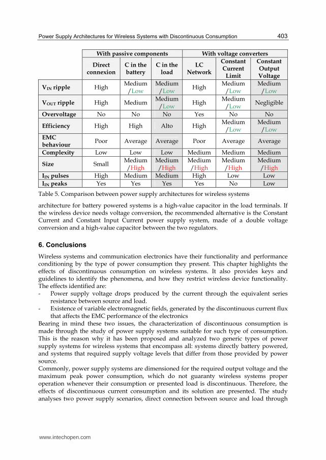
Table 5. Comparison between power supply architectures for wireless systems
architecture for battery powered systems is a high-value capacitor in the load terminals. If the wireless device needs voltage conversion, the recommended alternative is the Constant Current and Constant Input Current power supply system, made of a double voltage conversion and a high-value capacitor between the two regulators.
6. Conclusions
Wireless systems and communication electronics have their functionality and performance conditioning by the type of power consumption they present. This chapter highlights the effects of discontinuous consumption on wireless systems. It also provides keys and guidelines to identify the phenomena, and how they restrict wireless device functionality. The effects identified are: - Power supply voltage drops produced by the current through the equivalent series
resistance between source and load. - Existence of variable electromagnetic fields, generated by the discontinuous current flux
that affects the EMC performance of the electronics Bearing in mind these two issues, the characterization of discontinuous consumption is made through the study of power supply systems suitable for such type of consumption. This is the reason why it has been proposed and analyzed two generic types of power supply systems for wireless systems that encompass all: systems directly battery powered, and systems that required supply voltage levels that differ from those provided by power source. Commonly, power supply systems are dimensioned for the required output voltage and the maximum peak power consumption, which do not guaranty wireless systems proper operation whenever their consumption or presented load is discontinuous. Therefore, the effects of discontinuous current consumption and its solution are presented. The study analyses two power supply scenarios, direct connection between source and load through
www.intechopen.com
Recent Advances in Wireless Communications and Networks
404
passive components, and voltage regulation. In such conditions, the most common architectures could be restricted to: - High-value capacitor in the load or the source. - Voltage converter with input current limit plus high-value capacitor al the load ends. - Current Limit and Constant Input Current power supply system made of two
converters, plus a high-value parallel capacitor between both converters. Comparing and analyzing the different architectures studied, summarized in Table 5, could be concluded that suitable architectures are: - A high-value capacitor in the load or power source. - Current Limited and Constant Input Current power supply system if it is required
conditioning the voltage levels. Unless two regulators architecture may appear cumbersome, it is interesting highlight that increasing the switching frequency of DC-DC converters make feasible the use of such regulators, as high-frequency allows the reduction the size of the inductor and capacitors required. In spite of there were identified valid architectures, the effects of the discontinuous consumption are not eliminated completely, as shows Fig. 24. None of the architectures gets an input current drain from the source constant. If it is placed a high-value capacitor close to the load, there is a high current surge at the connexion instant between power source and wireless system. This current surge damages the connector reducing its lifetime. Moreover, high-value capacitor or super-capacitor may not be feasible, for they do not fit in the mechanics. Consequently, a trade-off between size and maximum available capacity and performance must be achieved. If Current Limited and Constant Input Current power supply is used, the input current is discontinuous for consumptions below the maximum, Fig. 24(e). The direct consequence is variable current flux that produces electromagnetic fields.
7. References
B. Arbetter, R. Erikson & D. Maksimovic, DC-DC converter design for battery-operated systems, in Proceeding of IEEE Power Electronic Specialist Conference, 1995, vol. 1, pp. 103-109.
B. Sahu & G.A. Rincon-mora, A Low Voltage, Non-Inverting, Dynamic, Synchronous Buck-Boost Converter for Portable Applications, IEEE Transactions on Power Electronics, vol. 19, no. 2, Feb. 2004, pp. 443-452.
E. Dahlman, H. Ekström, A. Furuskär, Y. Jading, J. Karlsson, M. Lundevall & S. Parkvall, The 3G Long-Term Evolution - Radio Interface Concepts and Performance Evaluation, IEEE Vehicular Technology Conference (VTC) , Melbourne, Australia, May 2006.
K. Fazel & S. Kaiser, 2008, Multi-Carrier and Spread Spectrum Systems: From OFDM and MC-CDMA to LTE and WiMAX, 2nd Edition, John Wiley & Sons, ISBN 978-0-470-99821-2.
M. I. Montrose, 1996, Printed circuit Board Design techniques for EMC Compliance, Piscataway, NJ, IEEE Press.
R. W. Erikson, 1997, Fundamentals of Power Electronics, Chapman and Hall, 1st ed., New York.
Saft Rechargeable Battery Systems, 2008, Rechargeable Battery Systems Handbook, Available from: http://www.saftbatteries.com.
W. Schroeder, July 2007, Direct Battery Connection Benefits Portable Designs, White Paper, Semtech.
www.intechopen.com
Recent Advances in Wireless Communications and NetworksEdited by Prof. Jia-Chin Lin
ISBN 978-953-307-274-6Hard cover, 454 pagesPublisher InTechPublished online 23, August, 2011Published in print edition August, 2011
InTech EuropeUniversity Campus STeP Ri Slavka Krautzeka 83/A 51000 Rijeka, Croatia Phone: +385 (51) 770 447 Fax: +385 (51) 686 166www.intechopen.com
InTech ChinaUnit 405, Office Block, Hotel Equatorial Shanghai No.65, Yan An Road (West), Shanghai, 200040, China
Phone: +86-21-62489820 Fax: +86-21-62489821
This book focuses on the current hottest issues from the lowest layers to the upper layers of wirelesscommunication networks and provides “real-time†research progress on these issues. The authors havemade every effort to systematically organize the information on these topics to make it easily accessible toreaders of any level. This book also maintains the balance between current research results and theirtheoretical support. In this book, a variety of novel techniques in wireless communications and networks areinvestigated. The authors attempt to present these topics in detail. Insightful and reader-friendly descriptionsare presented to nourish readers of any level, from practicing and knowledgeable communication engineers tobeginning or professional researchers. All interested readers can easily find noteworthy materials in muchgreater detail than in previous publications and in the references cited in these chapters.
How to referenceIn order to correctly reference this scholarly work, feel free to copy and paste the following:
Jose Ignacio Garate and Jose Miguel de Diego (2011). Power Supply Architectures for Wireless Systems withDiscontinuous Consumption, Recent Advances in Wireless Communications and Networks, Prof. Jia-Chin Lin(Ed.), ISBN: 978-953-307-274-6, InTech, Available from: http://www.intechopen.com/books/recent-advances-in-wireless-communications-and-networks/power-supply-architectures-for-wireless-systems-with-discontinuous-consumption

© 2011 The Author(s). Licensee IntechOpen. This chapter is distributedunder the terms of the Creative Commons Attribution-NonCommercial-ShareAlike-3.0 License, which permits use, distribution and reproduction fornon-commercial purposes, provided the original is properly cited andderivative works building on this content are distributed under the samelicense.