power quality improvement of grid connected … · systems are interfaced to grid and loads using...
TRANSCRIPT
462 Khadeeja Najeer, Laly M.J
International Journal of Engineering Technology Science and Research
IJETSR
www.ijetsr.com
ISSN 2394 – 3386
Volume 4, Issue 5
May 2017
Power Quality Improvement of Grid Connected Photovoltaic
System Using DVSI
Khadeeja Najeer
P.G Scholar
Dept of EEE
GEC, Thrissur
Laly M.J
Professor
Dept of EEE
GEC, Thrissur
I) ABSTRACT
This paper proposes a dual voltage source inverter (DVSI) design to enhance the energy quality and reliability of the
micro grid system. The suggested scheme is made up of two inverters, which permits the micro grid to switch power
made by the sent out energy resources (DERs) and to compensate the neighborhood unbalanced and nonlinear loads.
The control algorithms are developed based on instantaneous symmetrical component theory (ISCT) to use DVSI in grid
sharing and grid injecting settings. The proposed method has increased dependability, lower bandwidth dependence on
the key inverter, less expensive due to decrease in filter size, and better usage of micro grid ability when using reduced
dc-link voltage score for the key inverter. The DVSI is manufactured by these features design a promising option for
micro grid providing hypersensitive lots. The control and topology algorithm are validated through comprehensive
simulation results.
Keywords: DVSI, Instantaneous Symmetrical Component Theory (ISCT), DERs.
II) INTRODUCTION
Technological progress and environmental concerns drive the power system to a paradigm shift with more
renewable energy sources integrated to the network by means of distributed generation (DG). These DG units
with coordinated control of local generation and storage facilities form a micro grid. In a micro grid, power
from different renewable energy sources such as fuel cells, photovoltaic (PV) systems, and wind energy
systems are interfaced to grid and loads using power electronic converters. A grid interactive inverter plays an
important role in exchanging power from the micro grid to the grid and the connected load. This micro grid
inverter can either work in a grid sharing mode while supplying a part of local load or in grid injecting mode,
by injecting power to the main grid. Maintaining power quality is another important aspect which has to be
addressed while the micro grid system is connected to the main grid. The proliferation of power electronics
devices and electrical loads with unbalanced nonlinear currents has degraded the power quality in the power
distribution network. Moreover, if there is a considerable amount of feeder impedance in the distribution
systems, the propagation of these harmonic currents distorts the voltage at the point of common coupling
(PCC). At the same instant, industry automation has reached to a very high level of sophistication, where
plants like automobile manufacturing units, chemical factories, and semiconductor industries require clean
power. For these applications, it is essential to compensate nonlinear and unbalanced load currents. In, a
voltage regulation and power flow control scheme for a wind energy system (WES) is proposed. A
distribution static compensator (DSTATCOM) is utilized for voltage regulation and also for active power
injection. The control scheme maintains the power balance at the grid terminal during the wind variations
using sliding mode control. A multifunctional power electronic converter for the DG power system is
described in. This scheme has the capability to inject power generated by WES and also to perform as a
harmonic compensator. Most of the reported literature in this area discuss the topologies and control
algorithms to provide load compensation capability in the same inverter in addition to their active power

463 Khadeeja Najeer, Laly M.J
International Journal of Engineering Technology Science and Research
IJETSR
www.ijetsr.com
ISSN 2394 – 3386
Volume 4, Issue 5
May 2017
injection. When a grid-connected inverter is used for active power injection as well as for load compensation,
the inverter capacity that can be utilized for achieving the second objective is decided by the available
instantaneous micro grid real power. Considering the case of a grid-connected PV inverter, the available
capacity of the inverter to supply the reactive power becomes less during the maximum solar insolation
periods. At the same instant, the reactive power to regulate the PCC voltage is very much needed during this
period. It indicates that providing multi functionalities in a single inverter degrades either the real power
injection or the load compensation capabilities.
III) PROPOSED DUAL VOLTAGESOURCE INVERTER
i) System Topology
The proposed DVSI topology is shown inFig. It consists of a neutral point clamped(NPC) inverter to realize
AVSI and a threeleginverter for MVSI. These areconnected to grid at the PCC and supplyinga nonlinear and
unbalanced load. Thefunction of the AVSI is to compensate thereactive, harmonics, and
unbalancecomponents in load currents. Here, loadcurrents in three phases arerepresented byila, ilb, and ilc,
respectively. Also, ig(abc),iμgm(abc), and iμgx(abc) show gridcurrents, MVSI currents, and AVSI currentsin
three phases, respectively. The dc link ofthe AVSI utilizes a split capacitor topology,with two capacitors C1
and C2. The MVSIdelivers the available power at distributedenergy resource (DER) to grid. The DERcan be a
dc source or an ac source withrectifier coupled to dc link. Usually,renewable energy sources like fuel cell
andPV generate power at variable low dcvoltage, while the variable speed windturbines generate power at
variable acvoltage. Therefore, the power generated from these sources use a power conditioning stage before
it is connected to the input of MVSI. In this study, DER is being represented as a dc source. An inductor
filteris used to eliminate the high-frequency switching components generated due to theswitching of power
electronic switches inthe inverters. The system considered in thisstudy is assumed to have some amount
offeeder resistance Rgand inductance Lg. Dueto the presence of this feeder impedance,PCC voltage is affected
with harmonics.Section V describes the extraction offundamental positive sequence of PCCvoltages and
control strategy for thereference current generation of two invertersin DVSI scheme.
Fig.1. Topology of proposed DVSI scheme.

464 Khadeeja Najeer, Laly M.J
International Journal of Engineering Technology Science and Research
IJETSR
www.ijetsr.com
ISSN 2394 – 3386
Volume 4, Issue 5
May 2017
IV) DESIGN OF DVSI PARAMETERS
i) AVSI:
The important parameters of AVSI like dclinkvoltage (Vdc), dc storage capacitors (C1and C2), interfacing
inductance (Lfx), andhysteresis band (±hx) are selected based onthe design method of split
capacitorDSTATCOM topology. The dc-linkvoltage across each capacitor is taken as1.6times the peak of
phase voltage. The totaldc-link voltage reference (Vdcref ) is foundto be 1040 V. Values of dc capacitors
ofAVSI are chosen based on the change in dclinkvoltage during transients. Let total loadrating is S kVA. In
the worst case, the loadpower may vary fromminimum to maximum, i.e., from 0 to S kVA. AVSIneeds to
exchange real power duringtransient to maintain the load powerdemand. This transfer of real power duringthe
transient will result in deviation ofcapacitor voltage from its reference value. Assume that the voltage
controller takes n
cycles, i.e., nTseconds to act, where T is thesystem time period. Hence, maximumenergy exchange by AVSI
during transientwill be nST. This energy will be equal tochange in the capacitor stored energy.Therefore
where Vdcr and Vdc1 are the reference dcvoltage and maximum permissible dcvoltage across C1 during
transient,respectively. Here, S =5 kVA, Vdcr = 520 V,Vdc1 = 0.8 ∗Vdcr or 1.2 ∗Vdcr, n = 1, andT = 0.02 s.
Substituting these values in (1),he dclink capacitance (C1) is calculated tobe 2000 μF. Same value of
capacitance isselected for C2. The interfacing inductanceis given by
Assuming a maximum switching frequency(fmax) of 10 kHz and hysteresis band (hx) as5%of load current
(0.5 A), the value of Lfxis calculated to be 26 mH.
ii) MVSI:
The MVSI uses a three-leg invertertopology. Its dc-link voltage is obtained as1.15 * Vml, where Vmlis the peak
value ofline voltage. This is calculated to be 648 V.Also,MVSI supplies a balanced sinusoidalcurrent at unity
power factor. So, zerosequence switching harmonics will be
absent in the output current of MVSI. Thisreduces the filter requirement for MVSI ascompared to AVSI . In
this analysis, a filterinductance (Lfm) of 5 mH is used.
V) CONTROL STRATEGY FOR DVSISCHEME
i) Fundamental Voltage Extraction
The control algorithm for reference currentgeneration using ISCT requires balancedsinusoidal PCC voltages.
Because of thepresence of feeder impedance, PCC voltagesare distorted. Therefore, the fundamentalpositive
sequence components of the PCCvoltages are extracted for the referencecurrent generation. To convert the
distortedPCC voltages to balanced sinusoidal
voltages, dq0 transformation is used. ThePCC voltages in natural reference frame(vta, vtb, and vtc) are first
transformed intodq0 reference frame as given by

465 Khadeeja Najeer, Laly M.J
International Journal of Engineering Technology Science and Research
IJETSR
www.ijetsr.com
ISSN 2394 – 3386
Volume 4, Issue 5
May 2017
In order to get θ, a modified synchronousreference frame (SRF) phase locked loop(PLL) is used. It
mainlyconsists of a proportional integral (PI)controller and an integrator. In this PLL, theSRF terminal voltage
in q-axis (vtq) iscompared with 0 V and the error voltagethus obtained is given to the PI controller. The
frequency deviation Δωis then added tothe reference frequency ω0 and finally givento the integrator to get θ.
It can be provedthat, when, θ = ω0 t and by using the Park’stransformation matrix (C), q-axis voltage indq0
frame becomes zero and hence the PLLwill be locked to the reference frequency
(ω0).
ii) Symmetrical ComponentTheory
ISCT was developed primarily forunbalanced and nonlinear loadcompensations by active power filters.
Thesystem topology shown in Fig.2 is used forrealizing the reference current for the
compensator. The ISCT for loadcompensation is derived based on thefollowing three conditions.
Fig.2. Schematic of an unbalanced andnonlinear load compensation scheme.
466 Khadeeja Najeer, Laly M.J
International Journal of Engineering Technology Science and Research
IJETSR
www.ijetsr.com
ISSN 2394 – 3386
Volume 4, Issue 5
May 2017
1) The source neutral current must bezero. Therefore
2) The phase angle between thefundamental positive sequencevoltage (v+ta1) and source current
(isa) is φ
3) The average real power of the load(Pl) should be supplied by the source
Solving the above three equations, thereference source currents can be obtained as
A modification in the control algorithm isrequired, when it is used for DVSI scheme.The following section
discusses theformulation of control algorithm for DVSIscheme. The source currents, is(abc) andfilter currents
if(abc) will be equivalentlyrepresented as grid currents ig(abc) andAVSI currents iμgx(abc), respectively, infurther
sections.
VI) ADVANTAGES OF THE DVSI SCHEME
The various advantages of the proposed DVSI scheme over a single inverter scheme with multifunctional
capabilities are discussed here as follows:
i) Increased Reliability: DVSI scheme has increased reliability, due to the reduction in failure rate of
components and the decrease in system down time cost. In this scheme, the total load current is shared
between AVSI and MVSI and hence reduces the failure rate of inverter switches. Moreover, if one inverter
fails, the other can continue its operation. This reduces the lost energy and hence the down time cost. The
reduction in system down time cost improves the reliability.
ii) Reduction in Filter Size: In DVSI scheme, the current supplied by each inverter is reduced and hence the
current rating of individual filter inductor reduces. This reduction in current rating reduces the filter size. Also,
in this scheme, hysteresis current control is used to track the inverter reference currents. The filter inductance
is decided by the inverter switching frequency. Since the lower current rated semiconductor device can be
switched at higher switching frequency, the inductance of the filter can be lowered. This decrease in
inductance further reduces the filter size.
iii) Improved Flexibility: Both the inverters are fed from separate dc links which allow them to operate
independently, thus increasing the flexibility of the system. For instance, if the dc link of the main inverter is
disconnected from the system, the load compensation capability of the auxiliary inverter can still be utilized.
iv) Better Utilization of Microgrid Power: DVSI scheme helps to utilize full capacity of MVSI to transfer
the entire power generated by DG units as real power to ac bus, as there is AVSI for harmonic and reactive
power compensation. This increases the active power injection capability of DGs in micro grid.
v) Reduced DC-Link Voltage Rating: Since, MVSI is not delivering zero sequence load current
components, a single capacitor three-leg VSI topology can be used. Therefore, the dclink voltage rating of
MVSI is reduced approximately by 38%, as compared to a single inverter system with split capacitor VSI
topology

467 Khadeeja Najeer, Laly M.J
International Journal of Engineering Technology Science and Research
IJETSR
www.ijetsr.com
ISSN 2394 – 3386
Volume 4, Issue 5
May 2017
VII)SIMULATION RESULTS
Fig.3. Simulink diagram of DVSI.
i) Grid Sharing Mode
Fig.4. Real powerof load.

468 Khadeeja Najeer, Laly M.J
International Journal of Engineering Technology Science and Research
IJETSR
www.ijetsr.com
ISSN 2394 – 3386
Volume 4, Issue 5
May 2017
Fig.5. Real power of grid.
Fig.6. Real power by MVSI.
469 Khadeeja Najeer, Laly M.J
International Journal of Engineering Technology Science and Research
IJETSR
www.ijetsr.com
ISSN 2394 – 3386
Volume 4, Issue 5
May 2017
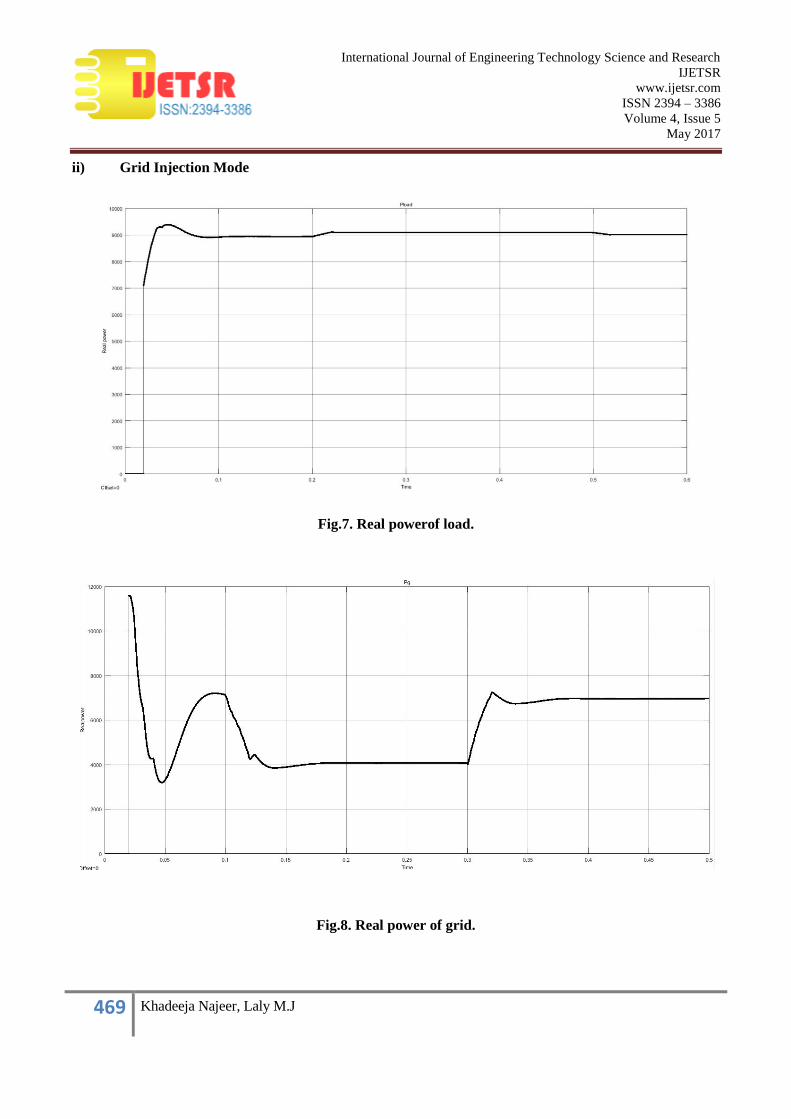
ii) Grid Injection Mode
Fig.7. Real powerof load.
Fig.8. Real power of grid.
470 Khadeeja Najeer, Laly M.J
International Journal of Engineering Technology Science and Research
IJETSR
www.ijetsr.com
ISSN 2394 – 3386
Volume 4, Issue 5
May 2017
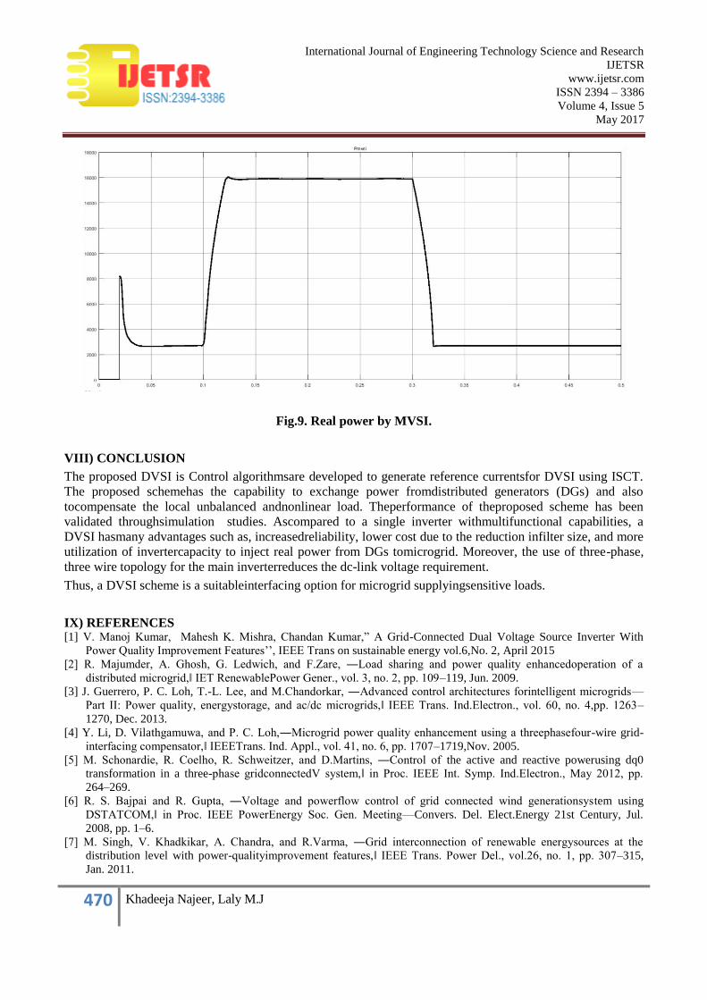
Fig.9. Real power by MVSI.
VIII) CONCLUSION
The proposed DVSI is Control algorithmsare developed to generate reference currentsfor DVSI using ISCT.
The proposed schemehas the capability to exchange power fromdistributed generators (DGs) and also
tocompensate the local unbalanced andnonlinear load. Theperformance of theproposed scheme has been
validated throughsimulation studies. Ascompared to a single inverter withmultifunctional capabilities, a
DVSI hasmany advantages such as, increasedreliability, lower cost due to the reduction infilter size, and more
utilization of invertercapacity to inject real power from DGs tomicrogrid. Moreover, the use of three-phase,
three wire topology for the main inverterreduces the dc-link voltage requirement.
Thus, a DVSI scheme is a suitableinterfacing option for microgrid supplyingsensitive loads.
IX) REFERENCES [1] V. Manoj Kumar, Mahesh K. Mishra, Chandan Kumar,” A Grid-Connected Dual Voltage Source Inverter With
Power Quality Improvement Features’’, IEEE Trans on sustainable energy vol.6,No. 2, April 2015
[2] R. Majumder, A. Ghosh, G. Ledwich, and F.Zare, ―Load sharing and power quality enhancedoperation of a
distributed microgrid,‖ IET RenewablePower Gener., vol. 3, no. 2, pp. 109–119, Jun. 2009.
[3] J. Guerrero, P. C. Loh, T.-L. Lee, and M.Chandorkar, ―Advanced control architectures forintelligent microgrids—
Part II: Power quality, energystorage, and ac/dc microgrids,‖ IEEE Trans. Ind.Electron., vol. 60, no. 4,pp. 1263–
1270, Dec. 2013.
[4] Y. Li, D. Vilathgamuwa, and P. C. Loh,―Microgrid power quality enhancement using a threephasefour-wire grid-
interfacing compensator,‖ IEEETrans. Ind. Appl., vol. 41, no. 6, pp. 1707–1719,Nov. 2005.
[5] M. Schonardie, R. Coelho, R. Schweitzer, and D.Martins, ―Control of the active and reactive powerusing dq0
transformation in a three-phase gridconnectedV system,‖ in Proc. IEEE Int. Symp. Ind.Electron., May 2012, pp.
264–269.
[6] R. S. Bajpai and R. Gupta, ―Voltage and powerflow control of grid connected wind generationsystem using
DSTATCOM,‖ in Proc. IEEE PowerEnergy Soc. Gen. Meeting—Convers. Del. Elect.Energy 21st Century, Jul.
2008, pp. 1–6.
[7] M. Singh, V. Khadkikar, A. Chandra, and R.Varma, ―Grid interconnection of renewable energysources at the
distribution level with power-qualityimprovement features,‖ IEEE Trans. Power Del., vol.26, no. 1, pp. 307–315,
Jan. 2011.
471 Khadeeja Najeer, Laly M.J
International Journal of Engineering Technology Science and Research
IJETSR
www.ijetsr.com
ISSN 2394 – 3386
Volume 4, Issue 5
May 2017
[8] H.-G. Yeh, D. Gayme, and S. Low, ―AdaptiveVAR control for distribution circuits withphotovoltaic generators,‖
IEEE Trans. Power Syst.,vol. 27, no. 3, pp. 1656–1663, Aug. 2012.
[9] C. Demoulias, ―A new simple analytical methodfor calculating the optimum inverter size in gridconnected PV
plants,‖ Electr. Power Syst. Res., vol.80, no. 10, pp. 1197–1204, 2010.
[10] R. Tonkoski, D. Turcotte, and T. H. M. ELFouly,―Impact of high PV penetration on voltageprofiles in residential
neighborhoods,‖ IEEE Trans.Sustain. Energy, vol. 3, no. 3, pp. 518–527, Jul. 2012.
[11] P. Rodriguez et al., ―A stationary referenceframe grid synchronization system for three-phasegrid-connected power
converters under adverse gridconditions,‖ IEEE Trans. Power Electron., vol. 27,no. 1, pp. 99–112, Jan. 2012.
[12] S. Iyer, A. Ghosh, and A. Joshi, ―Invertertopologies for DSTATCOM applications—Asimulation study,‖ Electr.
Power Syst. Res., vol. 75,no. 23, pp. 161–170, 2005.
[13] Y. Tang, P. C. Loh, P. Wang, F. H. Choo, and F.Gao, ―Exploring inherent damping characteristic ofLCL filters for
three-phase grid-connected voltagesource inverters,‖ IEEE Trans. Power Electron., vol.27, no. 3, pp. 1433–1443,
Mar. 2012.