power-performance simulation and design strategies for single-chip heterogeneous multiprocessors...
TRANSCRIPT
Power-Performance Simulation and Design Strategies for
Single-Chip Heterogeneous Multiprocessors
Salah Abdel-MageidFeb. 28, 2008
Agenda
Introduction Contributions A Point in the Design Space MESH Simulator First Contribution: Spatial Voltage Scaling Second Contribution: Power Model Third Contribution: Mixing a spatial voltage
scaling and a dynamic shutdown Conclusion
Introduction
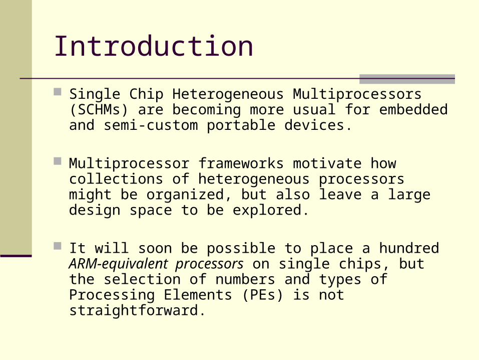
Single Chip Heterogeneous Multiprocessors (SCHMs) are becoming more usual for embedded and semi-custom portable devices.
Multiprocessor frameworks motivate how collections of heterogeneous processors might be organized, but also leave a large design space to be explored.
It will soon be possible to place a hundred ARM-equivalent processors on single chips, but the selection of numbers and types of Processing Elements (PEs) is not straightforward.
Introduction: Processing Element (PE)
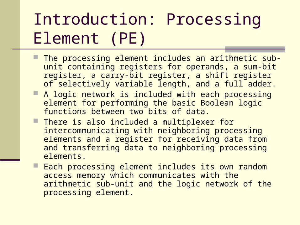
The processing element includes an arithmetic sub-unit containing registers for operands, a sum-bit register, a carry-bit register, a shift register of selectively variable length, and a full adder.
A logic network is included with each processing element for performing the basic Boolean logic functions between two bits of data.
There is also included a multiplexer for intercommunicating with neighboring processing elements and a register for receiving data from and transferring data to neighboring processing elements.
Each processing element includes its own random access memory which communicates with the arithmetic sub-unit and the logic network of the processing element.

Introduction
A primary motivation for designing SCHMs is to exploit new design strategies at the system level to save power.
There are two well-known examples for saving power:(1) Substituting multiple PEs at lower clock rates for one at a higher clock rate.(2) Turning off PEs when they are not needed.

Contributions
Introducing a new design strategy enabled by the high level power-performance simulator, MESH (called Spatial Voltage Scaling)
Mixing a spatial voltage scaling and a dynamic shutdown method
Extending MESH simulator into a power-performance simulator.
A Point in the Design Space
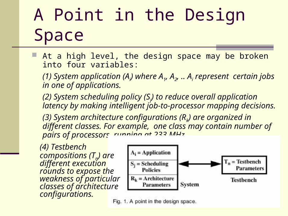
At a high level, the design space may be broken into four variables:
(1) System application (Ai) where A1, A2, .. Ai represent certain jobs in one of applications.
(2) System scheduling policy (Sj) to reduce overall application latency by making intelligent job-to-processor mapping decisions.
(3) System architecture configurations (Rk) are organized in different classes. For example, one class may contain number of pairs of processors running at 233 MHz.
(4) Testbench compositions (Tn) are different execution rounds to expose the weakness of particular classes of architecture configurations.
A Point in the Design Space
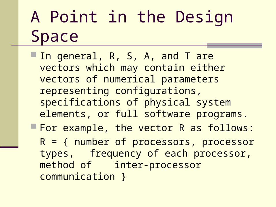
In general, R, S, A, and T are vectors which may contain either vectors of numerical parameters representing configurations, specifications of physical system elements, or full software programs.
For example, the vector R as follows:
R = { number of processors, processor types, frequency of each processor, method of inter-processor communication }
MESH
MESH stands for Modeling Environment for Software and Hardware, and is considered as a performance simulator that permits the designer to efficiently evaluate the performance effects of design space in the software, hardware (numbers and types of PEs), scheduling decisions, and communications (memory arbitration and network-style protocols) across multiple PEs on a chip.
In MESH simulator, system performance is simulated by resolving software execution into physical timing using high-level models of processor capabilities, with thread and message sequence determined by schedulers.
Layered Logical and Physical Design Elements in MESH
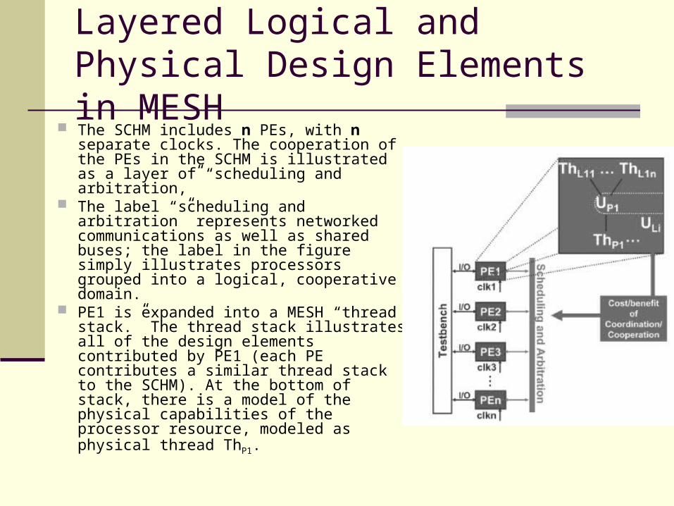
The SCHM includes n PEs, with n separate clocks. The cooperation of the PEs in the SCHM is illustrated as a layer of “scheduling and arbitration,”
The label “scheduling and arbitration” represents networked communications as well as shared buses; the label in the figure simply illustrates processors grouped into a logical, cooperative domain.
PE1 is expanded into a MESH “thread stack.” The thread stack illustrates all of the design elements contributed by PE1 (each PE contributes a similar thread stack to the SCHM). At the bottom of stack, there is a model of the physical capabilities of the processor resource, modeled as physical thread ThP1.

Threads’ Basic-Types in MESH
Each unique PE represents a different physical capability within the SCHM, which can be programmed to carry out concurrent behavior. This programming is captured as a collection of logical threads, ThL11; . . . ; ThL1n, shown at the top of the expanded view.
The basic types of threads in MESH as follows:
(1) ThLij: One of j logical threads (software) that will execute on processor i.
(2) ThPi: A model of the ith physical resource in the system, such as a processor.
(3) UPi: A scheduler that selects logical threads intended to execute on resource ThPi.
(4)ULi: A logical scheduler that can schedule M threads to N resources.
First Contribution: Spatial Voltage Scaling
Spatial voltage scaling is defined as a mix of dynamic voltage scaling and processor-rich design.
Dynamic voltage scaling is a technique that matches the execution frequency and voltage level of a given processor to certain application at runtime (linear relation).
Processor-rich design assumes n processors executing at a frequency (f/n) can be substituted for a single processor executing at frequency (f) for greatly reduced overall power.
Spatial voltage scaling seeks to find not only n, but a set of fi, one for each processor in the system.
Thus, n processors may be substituted for a single processor where the set of processors has a set of frequencies, { f1; . . . ; fn }. The frequency of each processor in the system is fixed at design time.
For example, spatially scaled configurations consisted of three pairs of processors operating at some f < 233 MHz, 2f/3, and f/3.
Experiments Authors run a set of experiments using MESH simulator to test the
suggestion that a spatially voltage scaled design could reduce overall power consumption while maintaining performance.
Assume the following document example:A = {gzip; wavelet transform; zero-tree quantization}T = {T1; T2; T3};S= {job-type-aware (SJT) [with dynamic shutdown (SJTDS)],
job-size-aware )SJS) [ with dynamic shutdown (SJSDS)] };R = {{ number of; type of; and operating frequency of
Processors }; shared memory communication }; The authors create a baseline design which demonstrates the
value of the high-level simulator, R0. The baseline architecture consists of one ARM and one
DSP(Digital Signal Processor), each executing at 233 MHz with a 1.65 V supply voltage, consuming 4.49 W and 4.62 W for the ARM and DSP, respectively.
Application Part
The baseline software design consists of three thread types that can execute on either processor type:
(1)The text portions are processed by a thread that runs gzip compression.
Each image compression requires two threads: (2)wavelet transform and
(3) zero-tree quantization. The execution time of a given gzip job is
approximately twice as fast on an ARM as it is on a DSP.
Testbench Part
Each document is injected into the system at a Poisson rate defined by the arrival rate in T.
T1 represents a class of documents where job size is distributed; it contains three text-image pairs: one large, one medium, one small.
T2 represents a class of documents where the amount of data in each size category is distributed; it contains seven text-image pairs: one large, two medium, four small.
T3 ,which contains 15 large images, represents a worst-case document. T3 is worst case because each processed image requires two jobs and each job is large.
These testbenches are chosen to expose the weaknesses of particular classes of architecture configurations.
Secluding Policies Part
SJT and SJS are designed to reduce overall document latency by making intelligent job-to-processor mapping decisions. SJT attempts only to map jobs to optimal processors based on job type. SJS extends SJT by taking into account the job size when making mapping decisions.
SJTDS and SJSDS are designed to dramatically reduce energy consumption by turning off whole PEs if they have been idle longer than a threshold.

Architecture Part
All configurations, Rk, have the same number of ARM as DSP processors, organized in pairs according to operating frequency. The devices complement each other in computational ability with respect to the application.
The architecture configurations can be broken into four classes:
(1) Base configurations
(2) Static voltage scaling configurations
(3) spatial voltage scaling configurations
(4) static/spatial hybrid configurations.
Architecture Configuration Classes
Base configurations consist of one to three pairs of processors operating at 233 MHz.
Static voltage scaling configurations consist of three to five pairs of processors operating at some f < 233 MHz.
Base and statically scaled configurations use SJT (or SJTDS) for job scheduling.
Spatial voltage scaling configurations consist of three pairs of processors operating at some f < 233 MHz, 2f/3, and f/3.
Hybrid configurations consist of four pairs of processors, two of which operated at some f < 233 MHz and two of which operated at 2f/3 and f/3, respectively.
Spatial scaling and hybrid configurations use SJS (or SJSDS) for job scheduling.
Second Contribution: Power Model
A power signature is an energy per cycle value in effect while a given fragment is executing on a given processor.
These fragments are constructed ( as a second contribution) to isolate the power consumption of individual instructions.
Processors are modeled to consume no energy when they are off.
First Power Signature
The first power signature characterizes the cost of executing the different programs in the example application.
This signature is calculated by taking the average energy per cycle cost of the programs.
Second Power Signature
A second power signature is used to model the power consumption of processors that are not turned off, but are not computing anything useful.
This signature captures processor behavior when portions of the processor go relatively unutilized, which the processor is not asleep and dissipates power.
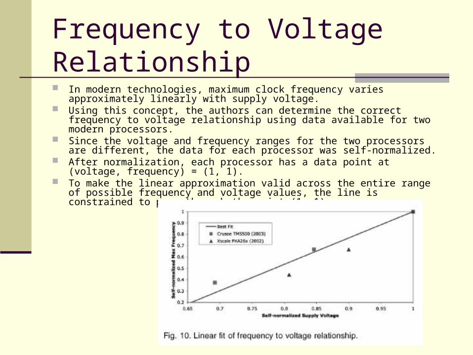
Frequency to Voltage Relationship In modern technologies, maximum clock frequency varies approximately linearly
with supply voltage. Using this concept, the authors can determine the correct frequency to voltage
relationship using data available for two modern processors. Since the voltage and frequency ranges for the two processors are different, the
data for each processor was self-normalized. After normalization, each processor has a data point at (voltage, frequency) = (1,
1). To make the linear approximation valid across the entire range of possible
frequency and voltage values, the line is constrained to pass through the point (1, 1).
Frequency to Voltage Relationship
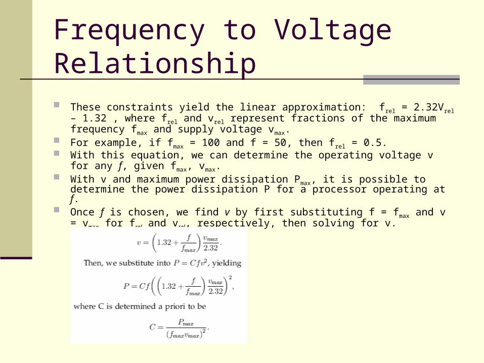
These constraints yield the linear approximation: frel = 2.32Vrel – 1.32 , where frel and vrel represent fractions of the maximum frequency fmax and supply voltage vmax.
For example, if fmax = 100 and f = 50, then frel = 0.5. With this equation, we can determine the operating voltage v for any f, given fmax,
vmax. With v and maximum power dissipation Pmax, it is possible to determine the
power dissipation P for a processor operating at f. Once f is chosen, we find v by first substituting f = fmax and v = vmax for frel and vrel,
respectively, then solving for v.

Results
All three testbenches are run on 10 architectures and a baseline architecture (total = 11 architectures)
The subset of architectures with the best latency in these first tests are then chosen for a second round of tests.
Table 1 shows the groupings of architectures by design strategy.
In the chart that follows, the legend shows the architecture parameters Rk
Each number in the legend represents a pair of ARM and DSP PEs. For example, for the baseline architecture R0, “233” denotes two PEs: one ARM and one DSP, each operating at 233 MHz.

Results
Normalized Average Latency at any case is worse than the base case’s for any of the three testbenches. The only architectures that perform better than the base case across all Tn are R4, R8, and R9.
The entire statically scaled class of architectures (R1-R3) is eliminated because of its performance in T1.
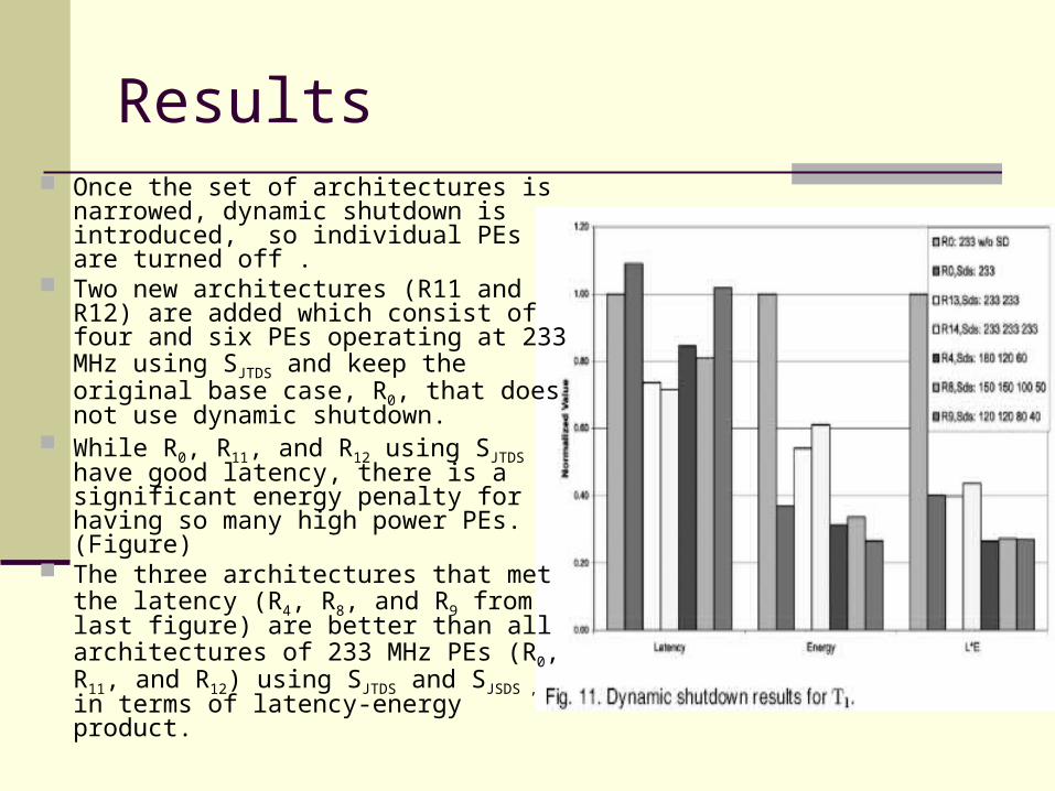
Results Once the set of architectures is
narrowed, dynamic shutdown is introduced, so individual PEs are turned off .
Two new architectures (R11 and R12) are added which consist of four and six PEs operating at 233 MHz using SJTDS and keep the original base case, R0, that does not use dynamic shutdown.
While R0, R11, and R12 using SJTDS have good latency, there is a significant energy penalty for having so many high power PEs. (Figure)
The three architectures that met the latency (R4, R8, and R9 from last figure) are better than all architectures of 233 MHz PEs (R0, R11, and R12) using SJTDS and SJSDS , in terms of latency-energy product.

Results This Figure shows the energy
and latency-energy product for the final candidate architectures exercised by T1 and T3.
R9 consumes only 45 percent as much energy as the base case under T3 and 27 percent under T1.
Its latency-energy product is 26 percent of the base case’s for T3, a 49 percent improvement over the next best performer.
R9 using SJSDS is the overall optimal solution, performing as well as R4 and R8 under T1, but It’s the best in comparison to them under T3.
Third Contribution
Mixing a spatial voltage scaling and a dynamic shutdown reduces both power and latency over a baseline design that use dynamic shutdown and do not use spatial voltage scaling.
This fact appeared in last figure.
Conclusion A novel design strategy, spatial voltage scaling, is introduced
and enabled by the early, high-level power performance simulator, MESH.
The power modeling extensions to MESH as described in this paper enabled the application of this design strategy.
The final design was discovered using spatial voltage scaling and dynamic shutdown. It reduces both power and latency over a baseline design that used dynamic shutdown, but did not use spatial voltage scaling.
The optimal design achieves an average of 66 percent energy improvement over a baseline case and an average of 15 percent latency improvement.
The latency-energy product of the final design is a 49 percent improvement over the next best performer
The optimal design is a hybrid statically/spatially scaled system. Its discovery required a combination of a strategic way of exploring the design space, enabled by high-level simulation.