power management integrated circuit · 2020-03-30 · power management integrated circuit...
TRANSCRIPT

Product structure : Silicon monolithic integrated circuit. This product has no designed protection against radioactive rays
1/118
www.rohm.com © 2018 ROHM Co., Ltd. All rights reserved. TSZ2211114001
TSZ02201-BD71847MWV-1-2
25.Sep.2018 Rev.0p84
Power Management Integrated Circuit BD71847MWV-DS1
General Description
BD71847MWV is a programmable Power Management IC (PMIC) for powering single-core, dual-core, and quad-core SoC’s such as NXP-i.MX 8M Mini. It is optimized for low BOM cost and compact solution footprint. It integrates 6 Buck regulators and 6 LDO’s to provide all the power rails required by the SoC and the commonly used peripherals.
QFN package and pinout support low cost Type 3 (non-HDI) PCB. Programmable power sequencing and output voltages, flexible power state control for easier system design and supports a wide variety of processors and system implementations.
Features 6 Buck Regulators 2.0 MHz Switching Frequency.
(BUCK1, BUCK2, BUCK5, BUCK7, and BUCK8). 1.5MHz Switching Frequency. (BUCK6)
Target Efficiency: 83% to 95%. Output Current & Voltage.
BUCK1: 3.0 A, 0.7 V to 1.3 V/10 mV step, DVS BUCK2: 3.0 A, 0.7 V to 1.3 V/10 mV step, DVS BUCK5: 3.0 A, 0.70 V to 1.35 V/8steps BUCK6: 3.0 A, 2.6 V to 3.3 V/100 mV step BUCK7: 1.5 A, 1.605 V to 1.995 V/8steps BUCK8: 3.0 A, 0.8 V to 1.4 V/10 mV step
6ch Linear Regulators LDO1: 10 mA, 3.0 V to 3.3 V, 1.6 V to 1.9 V LDO2: 10 mA, 0.9 V, 0.8 V LDO3: 300 mA, 1.8 V to 3.3 V LDO4: 250 mA, 0.9 V to 1.8 V LDO5: 300 mA, 0.8 V to 3.3 V LDO6: 300 mA, 0.9 V to 1.8 V
Power Mux Switch 1.8V Input: 500 mΩ(Max) 3.3V Input: 500 mΩ(Max)
32.768 kHz Crystal Oscillator Driver Power Button Detector
Protection and Monitoring: Soft Start, Power Rails Fault Detection, UVLO, OVP and TSD
OTP Configurable Power Sequencing OTP and Software Programmable Output Voltage,
Ramp rates. Hardware Signaling with SoC for Transition into or out
of Low Power States Interfaces: I2C: 100 kHz/400 kHz, 1 MHz Power-on Reset Output: POR_B, RTC_RESET_B, Watchdog Reset Input: WDOG_B: Power State Control:
PMIC_STBY_REQ, PMIC_ON_REQ, PWRON_B
Interrupt to SoC: IRQ_B Type3 PCB Applicable
Key Specifications
Input Voltage Range (VSYS): 2.7 V to 5.5 V SNVS State Current: 30 μA(Typ) SUSPEND State Current: 126 μA(Typ) IDLE State Current: 147 μA(Typ) RUN State Current: 147 μA(Typ) Operating Temperature Range: -40°C to +85°C
Applications
Streaming Media Boxes and Dongles AV Receivers and Wireless Sound Bars Industrial HMI, SBC, IPC and Panel Computer
Package W(Typ) x D(Typ) x H(Max) UQFN56BV7070 7.00mm x 7.00mm x 1.00mm
Datasheet

2/118 25.Sep.2018 Rev.0p84 © 2018 ROHM Co., Ltd. All rights reserved. www.rohm.com
TSZ22111 • 15 • 001
BD71847MWV-DS1
TSZ02201-BD71847MWV-1-2
Contents 1. Introduction ............................................................................................................................................................................. 7
1.1. Terminology .................................................................................................................................................................... 7 1.2. System Power Map & Typical Application Circuit ........................................................................................................... 8 1.3. Pin Configuration .......................................................................................................................................................... 10 1.4. Pin Description ............................................................................................................................................................. 11 1.5. I/O Equivalence Circuit ................................................................................................................................................. 12 1.6. Power Rail .................................................................................................................................................................... 14 1.7. Register Map ................................................................................................................................................................ 15 1.8. ESD .............................................................................................................................................................................. 17
2. Operating Conditions ............................................................................................................................................................ 18 2.1. Absolute Maximum Ratings (Ta=25 ˚C)........................................................................................................................ 18 2.2. Thermal Resistance ..................................................................................................................................................... 18 2.3. Recommended Operating Conditions .......................................................................................................................... 19 2.4. Current Consumption ................................................................................................................................................... 19 2.5. Power Reference and Detectors (UVLO) ..................................................................................................................... 20
3. Power State Control ............................................................................................................................................................. 21 3.1. Power Control Signals .................................................................................................................................................. 21
3.1.1. PWRON_B ........................................................................................................................................................... 22 3.1.2. PMIC_ON_REQ ................................................................................................................................................... 22 3.1.3. PMIC_STBY_REQ ............................................................................................................................................... 22 3.1.4. WDOG_B ............................................................................................................................................................. 22 3.1.5. RTC_RESET_B ................................................................................................................................................... 23 3.1.6. POR_B................................................................................................................................................................. 23
3.2. Power States ................................................................................................................................................................ 24 3.2.1. Power State Diagram ........................................................................................................................................... 24 3.2.2. Power State Register ........................................................................................................................................... 25 3.2.3. Power State Definition ......................................................................................................................................... 27 3.2.4. Power State Control Events ................................................................................................................................. 28
3.2.4.1. Reset Event ................................................................................................................................................. 28 3.2.4.2. Emergency Shutdown Event ....................................................................................................................... 30
3.2.5. Power State Transitions ....................................................................................................................................... 30 3.2.5.1. OFF to READY ............................................................................................................................................ 30 3.2.5.2. READY to SNVS ......................................................................................................................................... 31 3.2.5.3. SNVS to RUN .............................................................................................................................................. 34 3.2.5.4. RUN to IDLE ................................................................................................................................................ 36 3.2.5.5. IDLE to RUN ................................................................................................................................................ 36 3.2.5.6. RUN to SUSPEND ...................................................................................................................................... 36 3.2.5.7. SUSPEND to RUN ...................................................................................................................................... 36 3.2.5.8. IDLE to SUSPEND ...................................................................................................................................... 37 3.2.5.9. Emergency Shutdown ................................................................................................................................. 37 3.2.5.10. VR Fault ...................................................................................................................................................... 38 3.2.5.11. EMG to OFF ................................................................................................................................................ 42 3.2.5.12. EMG to READY ........................................................................................................................................... 43 3.2.5.13. EMG_STAY Condition ................................................................................................................................. 44 3.2.5.14. Warm Reset ................................................................................................................................................. 44 3.2.5.15. PWROFF ..................................................................................................................................................... 45 3.2.5.16. PWROFF to READY.................................................................................................................................... 47 3.2.5.17. PWROFF to SNVS ...................................................................................................................................... 47 3.2.5.18. PWRON_B Functionality ............................................................................................................................. 47
3.3. Power Sequence .......................................................................................................................................................... 49 3.3.1. Power ON Sequence ........................................................................................................................................... 49 3.3.2. Power OFF Sequence ......................................................................................................................................... 51 3.3.3. RUN to IDLE ........................................................................................................................................................ 55 3.3.4. IDLE to RUN ........................................................................................................................................................ 56 3.3.5. RUN to SUSPEND ............................................................................................................................................... 57 3.3.6. SUSPEND to RUN ............................................................................................................................................... 58 3.3.7. IDLE to SUSPEND .............................................................................................................................................. 59 3.3.8. Emergency Shutdown .......................................................................................................................................... 60 3.3.9. Warm Reset ......................................................................................................................................................... 61 3.3.10. Reset Source Indicators....................................................................................................................................... 62
4. I2C and Interrupt .................................................................................................................................................................. 63 4.1. I2C Bus Interface ......................................................................................................................................................... 63
4.1.1. I2C Bus Interface Overview ................................................................................................................................. 63 4.1.2. I2C Bus Interface Electrical Characteristics ......................................................................................................... 64 4.1.3. Device Addressing ............................................................................................................................................... 66 4.1.4. Write / Read Operation ........................................................................................................................................ 67
4.2. Interrupt ........................................................................................................................................................................ 68 4.2.1. Interrupt Overview ............................................................................................................................................... 68
5. Power Rails .......................................................................................................................................................................... 71

3/118 25.Sep.2018 Rev.0p84 © 2018 ROHM Co., Ltd. All rights reserved. www.rohm.com
TSZ22111 • 15 • 001
BD71847MWV-DS1
TSZ02201-BD71847MWV-1-2
5.1. Output Voltage Range .................................................................................................................................................. 71 5.2. Details of Buck ............................................................................................................................................................. 73
5.2.1. BUCK1 ................................................................................................................................................................. 73 5.2.1.1. BUCK1 Block Diagram ................................................................................................................................ 73 5.2.1.2. BUCK1 Electrical Characteristics ................................................................................................................ 74 5.2.1.3. BUCK1 Control ............................................................................................................................................ 75
5.2.2. BUCK2 ................................................................................................................................................................. 77 5.2.2.1. BUCK2 Block Diagram ................................................................................................................................ 77 5.2.2.2. BUCK2 Electrical Characteristics ................................................................................................................ 78 5.2.2.3. BUCK2 Control ............................................................................................................................................ 79
5.2.3. BUCK5 ................................................................................................................................................................. 81 5.2.3.1. BUCK5 Block Diagram ................................................................................................................................ 81 5.2.3.2. BUCK5 Electrical Characteristics ................................................................................................................ 82 5.2.3.3. BUCK5 Control ............................................................................................................................................ 83
5.2.4. BUCK6 ................................................................................................................................................................. 84 5.2.4.1. BUCK6 Block Diagram ................................................................................................................................ 84 5.2.4.2. BUCK6 Electrical Characteristics ................................................................................................................ 85 5.2.4.3. BUCK6 Control ............................................................................................................................................ 86
5.2.5. BUCK7 ................................................................................................................................................................. 87 5.2.5.1. BUCK7 Block Diagram ................................................................................................................................ 87 5.2.5.2. BUCK7 Electrical Characteristics ................................................................................................................ 88 5.2.5.3. BUCK7 Control ............................................................................................................................................ 89
5.2.6. BUCK8 ................................................................................................................................................................. 90 5.2.6.1. BUCK8 Block Diagram ................................................................................................................................ 90 5.2.6.2. BUCK8 Electrical Characteristics ................................................................................................................ 91 5.2.6.3. BUCK8 Control ............................................................................................................................................ 92
5.3. Details of LDO .............................................................................................................................................................. 93 5.3.1. LDO1 ................................................................................................................................................................... 93
5.3.1.1. LDO1 Block Diagram ................................................................................................................................... 93 5.3.1.2. LDO1 Electrical Characteristics ................................................................................................................... 94 5.3.1.3. LDO1 Control .............................................................................................................................................. 95
5.3.2. LDO2 ................................................................................................................................................................... 96 5.3.2.1. LDO2 Block Diagram ................................................................................................................................... 96 5.3.2.2. LDO2 Electrical Characteristics ................................................................................................................... 97 5.3.2.3. LDO2 Control .............................................................................................................................................. 97
5.3.3. LDO3 ................................................................................................................................................................... 98 5.3.3.1. LDO3 Block Diagram ................................................................................................................................... 98 5.3.3.2. LDO3 Electrical Characteristics ................................................................................................................... 99 5.3.3.3. LDO3 Control ............................................................................................................................................ 100
5.3.4. LDO4 ................................................................................................................................................................. 101 5.3.4.1. LDO4 Block Diagram ................................................................................................................................. 101 5.3.4.2. LDO4 Electrical Characteristics ................................................................................................................. 102 5.3.4.3. LDO4 Control ............................................................................................................................................ 103
5.3.5. LDO5 ................................................................................................................................................................. 104 5.3.5.1. LDO5 Block Diagram ................................................................................................................................. 104 5.3.5.2. LDO5 Electrical Characteristics ................................................................................................................. 105 5.3.5.3. LDO5 Control ............................................................................................................................................ 106
5.3.6. LDO6 ................................................................................................................................................................. 107 5.3.6.1. LDO6 Block Diagram ................................................................................................................................. 107 5.3.6.2. LDO6 Electrical Characteristics ................................................................................................................. 108 5.3.6.3. LDO6 Control ............................................................................................................................................ 109
5.4. MUXSW ..................................................................................................................................................................... 110 5.4.1. MUXSW Block Diagram ..................................................................................................................................... 110 5.4.2. MUXSW Electrical Characteristics ..................................................................................................................... 111
6. 32.768 kHz Crystal Oscillator Driver ................................................................................................................................... 112 6.1. 32.768 kHz Crystal Oscillator Driver Block Diagram .................................................................................................. 112 6.2. 32.768 kHz Crystal Oscillator Driver Electrical Characteristics .................................................................................. 112
7. Operational Notes .............................................................................................................................................................. 113 8. Ordering Information........................................................................................................................................................... 115 9. Marking Diagram ................................................................................................................................................................ 115 10. Physical Dimension and Packing Information ................................................................................................................ 116 11. Revision History ............................................................................................................................................................. 117
Figure Figure 1-1. System Power Map ............................................................................................................................................... 8 Figure 1-2. Typical Applications Circuit .................................................................................................................................... 9 Figure 1-3. Pin Configuration (TOP VIEW) ............................................................................................................................ 10 Figure 1-4. I/O Equivalence Circuit 1 ..................................................................................................................................... 12 Figure 1-5. I/O Equivalence Circuit 2 ..................................................................................................................................... 13 Figure 2-1. Power Reference and Detectors Block Diagram ................................................................................................. 20

4/118 25.Sep.2018 Rev.0p84 © 2018 ROHM Co., Ltd. All rights reserved. www.rohm.com
TSZ22111 • 15 • 001
BD71847MWV-DS1
TSZ02201-BD71847MWV-1-2
Figure 3-1. Power Control Signals of BD71847MWV ............................................................................................................ 21 Figure 3-2. Power State Transition ........................................................................................................................................ 24 Figure 3-3. Power Sub State Definition.................................................................................................................................. 26 Figure 3-4. VSYS Condition for moving to SNVS .................................................................................................................. 31 Figure 3-5. PMIC_ON_REQ Condition for moving to SNVS .................................................................................................. 31 Figure 3-6. PWRON_B Short Push Condition for moving to SNVS ....................................................................................... 32 Figure 3-7. PWRON_B Long Push Condition for moving to SNVS ........................................................................................ 32 Figure 3-8. Cold Reset Condition for moving to SNVS .......................................................................................................... 32 Figure 3-9. VSYS Condition for moving to RUN .................................................................................................................... 34 Figure 3-10. PMIC_ON_REQ Condition for moving to RUN .................................................................................................. 34 Figure 3-11. PWRON_B Short Push Condition for moving to RUN ....................................................................................... 35 Figure 3-12. PWRON_B Long Push Condition for moving to RUN ........................................................................................ 35 Figure 3-13. Cold Reset Condition for moving to RUN .......................................................................................................... 35 Figure 3-14. Example of VR Fault and Recovery Sequence (RCVLMT[3:0] = 2) .................................................................. 42 Figure 3-15. EMG to OFF Power State Transition ................................................................................................................. 42 Figure 3-16. EMG to READY Power State Transition (VSYS_UVLO) ................................................................................... 43 Figure 3-17. EMG to READY Power State Transition (Die Temperature) .............................................................................. 43 Figure 3-18. Warm Reset by WDOG_B ................................................................................................................................. 44 Figure 3-19. Cold Reset Duration Time set by PONT[3:0] ..................................................................................................... 46 Figure 3-20. Power Button Block Diagram ............................................................................................................................. 47 Figure 3-21. Power ON Sequence ......................................................................................................................................... 49 Figure 3-22. Power OFF Sequence (To SNVS) ..................................................................................................................... 51 Figure 3-23. Power OFF Sequence (To READY) .................................................................................................................. 53 Figure 3-24. RUN to IDLE ...................................................................................................................................................... 55 Figure 3-25. IDLE to RUN ...................................................................................................................................................... 56 Figure 3-26. RUN to SUSPEND ............................................................................................................................................ 57 Figure 3-27. SUSPEND to RUN ............................................................................................................................................ 58 Figure 3-28. IDLE to SUSPEND ............................................................................................................................................ 59 Figure 3-29. Emergency Shutdown ....................................................................................................................................... 60 Figure 3-30. Warm Reset (SWRESET) ................................................................................................................................. 61 Figure 3-31. Warm Reset (WDOG_B) ................................................................................................................................... 61 Figure 3-32. Warm Reset (PWRON_B Long Push) ............................................................................................................... 61 Figure 4-1. I2C (Slave) Block Diagram .................................................................................................................................. 63 Figure 4-2. I2C Bus Interface AC Timing ............................................................................................................................... 65 Figure 4-3. I2C Device Addressing ........................................................................................................................................ 66 Figure 4-4. I2C Write / Read Operation ................................................................................................................................. 67 Figure 4-5. IRQ_B Architecture Block Diagram ..................................................................................................................... 68 Figure 5-1. BUCK1 Block Diagram ........................................................................................................................................ 73 Figure 5-2. BUCK2 Block Diagram ........................................................................................................................................ 77 Figure 5-3. BUCK5 Block Diagram ........................................................................................................................................ 81 Figure 5-4. BUCK6 Block Diagram ........................................................................................................................................ 84 Figure 5-5. BUCK7 Block Diagram ........................................................................................................................................ 87 Figure 5-6. BUCK8 Block Diagram ........................................................................................................................................ 90 Figure 5-7. LDO1 Block Diagram ........................................................................................................................................... 93 Figure 5-8. LDO2 Block Diagram ........................................................................................................................................... 96 Figure 5-9. LDO3 Block Diagram ........................................................................................................................................... 98 Figure 5-10. LDO3 Voltage Source Switching ..................................................................................................................... 100 Figure 5-11. LDO4 Block Diagram ....................................................................................................................................... 101 Figure 5-12. LDO4 Voltage Source Switching ..................................................................................................................... 103 Figure 5-13. LDO5 Block Diagram ....................................................................................................................................... 104 Figure 5-14. LDO6 Block Diagram ....................................................................................................................................... 107 Figure 5-15. MUXSW Block Diagram .................................................................................................................................. 110 Figure 5-16. MUXSW Sequence ......................................................................................................................................... 111 Figure 6-1. 32.768 kHz Crystal Oscillator Driver Block Diagram ......................................................................................... 112 Figure 9-1. Marking Diagram ............................................................................................................................................... 115
Table
Table 1-1. Acronyms, Conventions and Terminology ............................................................................................................... 7 Table 1-2. Pin Description ...................................................................................................................................................... 11 Table 1-3. Power Rails and Output Signals ........................................................................................................................... 14 Table 1-4. Register Map ......................................................................................................................................................... 15 Table 1-5. REV - Revision Register ....................................................................................................................................... 15 Table 1-6. REGLOCK - Lock Register ................................................................................................................................... 16 Table 1-7. OTPVER – OTP Version Register ......................................................................................................................... 16 Table 1-8. ESD ...................................................................................................................................................................... 17 Table 2-1. Absolute Maximum Ratings................................................................................................................................... 18 Table 2-2. Thermal Resistance
(Note 1) ..................................................................................................................................... 18
Table 2-3. Recommended Operating Conditions ................................................................................................................... 19 Table 2-4. Current Consumption ............................................................................................................................................ 19

5/118 25.Sep.2018 Rev.0p84 © 2018 ROHM Co., Ltd. All rights reserved. www.rohm.com
TSZ22111 • 15 • 001
BD71847MWV-DS1
TSZ02201-BD71847MWV-1-2
Table 2-5. Power Reference and Detectors Electrical Characteristics ................................................................................... 20 Table 3-1. PWRON_B Electrical Characteristics .................................................................................................................... 22 Table 3-2. PMIC_ON_REQ Electrical Characteristics ............................................................................................................ 22 Table 3-3. PMIC_STBY_REQ Electrical Characteristics ........................................................................................................ 22 Table 3-4. WDOG_B Electrical Characteristics ...................................................................................................................... 22 Table 3-5. RTC_RESET_B Electrical Characteristics ............................................................................................................ 23 Table 3-6. POR_B Electrical Characteristics .......................................................................................................................... 23 Table 3-7. POW_STATE – Power State Register ................................................................................................................... 25 Table 3-8. Voltage Rails ON/OFF for Respective Power State .............................................................................................. 28 Table 3-9. Setting of Cold or Warm Reset Selection .............................................................................................................. 29 Table 3-10. SWRESET - Software Reset Register ................................................................................................................ 29 Table 3-11. PWRCTRL0 - Power Control 0 Register ............................................................................................................. 29 Table 3-12. Conditions from OFF to READY state ................................................................................................................. 30 Table 3-13. Conditions from READY to SNVS ....................................................................................................................... 31 Table 3-14. TRANS_COND0 - Transition Condition Select 0 Register .................................................................................. 33 Table 3-15. Conditions from SNVS to RUN ........................................................................................................................... 34 Table 3-16. Conditions from RUN to IDLE ............................................................................................................................. 36 Table 3-17. PWRCTRL1 - Power Control 1 Register ............................................................................................................. 36 Table 3-18. Conditions from IDLE to RUN ............................................................................................................................. 36 Table 3-19. Conditions from RUN to SUSPEND .................................................................................................................... 36 Table 3-20. Conditions from SUSPEND to RUN .................................................................................................................... 36 Table 3-21. Conditions from IDLE to SUSPEND .................................................................................................................... 37 Table 3-22. Conditions from SNVS, RUN, IDLE, SUSPEND, PWROFF to EMG ................................................................... 37 Table 3-23. VR FAULT threshold and monitoring condition.................................................................................................... 38 Table 3-24. VRFAULTEN - VR FAULT ON/OFF Register: Debugging Purpose ..................................................................... 39 Table 3-25. MVRFLTMASK0 - VR FAULT Mask 0 Register ................................................................................................... 39 Table 3-26. MVRFLTMASK1 - VR FAULT Mask 1 Register ................................................................................................... 40 Table 3-27. MVRFLTMASK2 - VR FAULT Mask 2 Register ................................................................................................... 40 Table 3-28. RCVCFG - Recovery Configuration Register ...................................................................................................... 41 Table 3-29. RCVNUM - Recovery Number Register .............................................................................................................. 41 Table 3-30. Conditions from EMG to OFF .............................................................................................................................. 42 Table 3-31. Conditions from EMG to READY ........................................................................................................................ 43 Table 3-32. Conditions for Stay at EMG................................................................................................................................. 44 Table 3-33. Conditions from RUN, IDLE, SUSPEND to PWROFF ........................................................................................ 45 Table 3-34. TRANS_COND1 - Transition Condition Select 1 Register .................................................................................. 45 Table 3-35. VR Summary After Power OFF Sequence .......................................................................................................... 46 Table 3-36. PWRONCONFIG0 - PWRON_B Configuration 0 Register.................................................................................. 47 Table 3-37. PWRONCONFIG1 - PWRON_B Configuration 1 Register.................................................................................. 48 Table 3-38. Power ON Sequence Timing Specification.......................................................................................................... 50 Table 3-39. Power OFF Sequence Timing Specification (To SNVS) ...................................................................................... 52 Table 3-40. Power OFF Sequence Timing Specification (To READY) ................................................................................... 54 Table 3-41. RUN to IDLE Timing Specification ...................................................................................................................... 55 Table 3-42. IDLE to RUN Timing Specification ...................................................................................................................... 56 Table 3-43. RUN to SUSPEND Timing Specification ............................................................................................................. 57 Table 3-44. SUSPEND to RUN Timing Specification ............................................................................................................. 58 Table 3-45. IDLE to SUSPEND Timing Specification ............................................................................................................. 59 Table 3-46. Emergency Shutdown Timing Specification ........................................................................................................ 60 Table 3-47. Warm Reset (SWRESET) Timing Specification .................................................................................................. 61 Table 3-48. Warm Reset (WDOG_B) Timing Specification .................................................................................................... 61 Table 3-49. Warm Reset (PWRON_B Long Push) Timing Specification ................................................................................ 61 Table 3-50. RESETSRC - Reset Source Indicator Register ................................................................................................... 62 Table 4-1. I2C Bus Interface DC Electrical Characteristics .................................................................................................... 64 Table 4-2. I2C Bus Interface AC Timing - Fast Mode ............................................................................................................. 65 Table 4-3. I2C_DEV - I2C Device Address Indicator Register ............................................................................................... 66 Table 4-4. Interrupt Event ...................................................................................................................................................... 68 Table 4-5. IRQ_B Electrical Characteristics ........................................................................................................................... 68 Table 4-6. IRQ - Interrupt Register ......................................................................................................................................... 69 Table 4-7. MIRQ – IRQ Mask Register .................................................................................................................................. 69 Table 4-8. IN_MON - Input Port Monitor Register .................................................................................................................. 70 Table 5-1. Output Voltage Range1 ......................................................................................................................................... 71 Table 5-2. Output Voltage Range2 ......................................................................................................................................... 72 Table 5-3. BUCK1 Electrical Characteristics .......................................................................................................................... 74 Table 5-4. BUCK1_CTRL - BUCK1 Control Register ............................................................................................................. 75 Table 5-5. BUCK1_VOLT_RUN - BUCK1 Voltage (RUN) Register ........................................................................................ 75 Table 5-6. BUCK1_VOLT_IDLE - BUCK1 Voltage (IDLE) Register ....................................................................................... 76 Table 5-7. BUCK1_VOLT_SUSP - BUCK1 Voltage (SUSPEND) Register ............................................................................ 76 Table 5-8. BUCK2 Electrical Characteristics .......................................................................................................................... 78 Table 5-9. BUCK2_CTRL - BUCK2 Control Register ............................................................................................................. 79 Table 5-10. BUCK2_VOLT_RUN - BUCK2 Voltage (RUN) Register ...................................................................................... 79 Table 5-11. BUCK2_VOLT_IDLE - BUCK2 Voltage (IDLE) Register ...................................................................................... 80

6/118 25.Sep.2018 Rev.0p84 © 2018 ROHM Co., Ltd. All rights reserved. www.rohm.com
TSZ22111 • 15 • 001
BD71847MWV-DS1
TSZ02201-BD71847MWV-1-2
Table 5-12. BUCK5 Electrical Characteristics ........................................................................................................................ 82 Table 5-13. BUCK5_CTRL - BUCK5 Control Register ........................................................................................................... 83 Table 5-14. BUCK5_VOLT - BUCK5 Voltage Register ........................................................................................................... 83 Table 5-15. BUCK6 Electrical Characteristics ........................................................................................................................ 85 Table 5-16. BUCK6_CTRL - BUCK6 Control Register ........................................................................................................... 86 Table 5-17. BUCK6_VOLT - BUCK6 Voltage Register ........................................................................................................... 86 Table 5-18. BUCK7 Electrical Characteristics ........................................................................................................................ 88 Table 5-19. BUCK7_CTRL - BUCK7 Control Register ........................................................................................................... 89 Table 5-20. BUCK7_VOLT - BUCK7 Voltage Register ........................................................................................................... 89 Table 5-21. BUCK8 Electrical Characteristics ........................................................................................................................ 91 Table 5-22. BUCK8_CTRL - BUCK8 Control Register ........................................................................................................... 92 Table 5-23. BUCK8_VOLT - BUCK8 Voltage Register ........................................................................................................... 92 Table 5-24. LDO1 Electrical Characteristics .......................................................................................................................... 94 Table 5-25. LDO1_VOLT - LDO1 Voltage Register ................................................................................................................ 95 Table 5-26. LDO2 Electrical Characteristics .......................................................................................................................... 97 Table 5-27. LDO2_VOLT - LDO2 Voltage Register ................................................................................................................ 97 Table 5-28. LDO3 Electrical Characteristics .......................................................................................................................... 99 Table 5-29. LDO3_VOLT - LDO3 Voltage Register .............................................................................................................. 100 Table 5-30. LDO4 Electrical Characteristics ........................................................................................................................ 102 Table 5-31. LDO4_VOLT - LDO4 Voltage Register .............................................................................................................. 103 Table 5-32. LDO5 Electrical Characteristics ........................................................................................................................ 105 Table 5-33. LDO5_VOLT - LDO5 Voltage Register .............................................................................................................. 106 Table 5-34. LDO6 Electrical Characteristics ........................................................................................................................ 108 Table 5-35. LDO6_VOLT - LDO6 Voltage Register .............................................................................................................. 109 Table 5-36. MUXSW Electrical Characteristics .................................................................................................................... 111 Table 5-37. SD_VSELECT Electrical Characteristics........................................................................................................... 111 Table 5-38. MUXSW Sequence Timing ................................................................................................................................ 111 Table 5-39. MUXSW_EN - MUXSW Enable Register .......................................................................................................... 111 Table 6-1. C32K_OUT Control Register ............................................................................................................................... 112 Table 6-2. 32.768 kHz Crystal Oscillator Driver Electrical Characteristics ........................................................................... 112

7/118 25.Sep.2018 Rev.0p84 © 2018 ROHM Co., Ltd. All rights reserved. www.rohm.com
TSZ22111 • 15 • 001
BD71847MWV-DS1
TSZ02201-BD71847MWV-1-2
1. Introduction 1.1. Terminology
Table 1-1. Acronyms, Conventions and Terminology
Term Definition
BOM Bill Of Materials
DAC Digital to Analog Converter
DVS Dynamic Voltage Scaling
FET Field Effect Transistor
I2C Inter-Integrated Circuit
IRQ Interrupt Request
LDO Low Drop-Out regulator
NTC Negative Temperature Coefficient. (a type of thermistor)
OCP Over Current Protection
OTP One Time Programmable memory
OVP Over Voltage Protection
PFM Pulse-Frequency Modulation
POR Power On Reset
PWM Pulse-Width Modulation
SMPS Switched Mode Power Supply
SoC System-On-a-Chip
UVLO Under Voltage-LockOut
VR Voltage Regulator

8/118 25.Sep.2018 Rev.0p84 © 2018 ROHM Co., Ltd. All rights reserved. www.rohm.com
TSZ22111 • 15 • 001
BD71847MWV-DS1
TSZ02201-BD71847MWV-1-2
1.2. System Power Map & Typical Application Circuit
Figure 1-1. System Power Map
32kHz
Crystal
Driver
0.8 V
0.8 V/0.9 V/ 1.0V
0.8 V/0.9 V
1.8V
0.8V
3.3V
1.8V
1.8V
1.2V
0.9V
VSYS(5V)
PMIC_STBY_REQ
HOST
I/F
BD71847MWV
I2C I/F
WDOG_B
PMIC_ON_REQ
POR_B
RTC_RESET_B
IRQ_B
XOUT
XIN
C32K_OUT
NVCC_DRAM
VDD_SOC
VDDA_0V8
PHY_0V8
VDD_ARM
VDD_GPU
VDD_VPU
VDD_DRAM
NVCC_SNVS
NVCC_3V3
VDD_SNVS
VDDA_1V8
VDDA_DRAM
NVCC_1V8
VDDA_1V2
(MIPI)
VDDA_0V9
(MIPI)
i.MX8M Mini
PWRON_B
150mA MUXSW1.8V/3.3V(SD CARD)1.8V
3.3V
SD_VSELECT
BUCK1 – DVS
3.0 A, 0.7 V to 1.3 V
/10 mV step
BUCK2 – DVS
3.0 A, 0.7 V to 1.3 V
/10 mV step
BUCK5
3.0 A, 0.70 V to 1.35 V
/ 8steps
BUCK8
3.0 A, 0.8 V to 1.4 V
/10 mV step
LDO1
10 mA, 3.0 V to 3.3 V
/1.6 V to 1.9 V
LDO2
10 mA,
0.9 V/0.8 V
BUCK6
3.0 A, 2.6 V to 3.3 V
/0.1 V step
LDO3
300 mA,
1.8 V to 3.3 V
LDO5
300 mA,
0.8 V to 3.3 V
BUCK7
1.5 A, 1.605 V to
1.995 V/ 8steps
LDO4
250 mA,
0.9 V to 1.8 V
LDO6
300 mA,
0.9 V to 1.8 V
1.10 V/1.20 V/1.35 V

9/118 25.Sep.2018 Rev.0p84 © 2018 ROHM Co., Ltd. All rights reserved. www.rohm.com
TSZ22111 • 15 • 001
BD71847MWV-DS1
TSZ02201-BD71847MWV-1-2
1.2. System Power Map & Typical Application Circuit - continued
Figure 1-2. Typical Applications Circuit
Register
Sequencer
INTLDO1P5 VREF
VDD_V1P5
VDD_V1P5
VDD_V1P5
AGND
VSYS
WDOG_B
BUCK1_FB
VSYS
BUCK1
(VDD_SOC
VDDA_0V8
PHY_0V8)
VDD_V1P5
VREF
SOC
VSYS
PGND (EXP-PAD)PGND
PGND
SCL
SDA
VDD_V1P5
TSD
Internal
Power On Reset
BD71847MWV
Voltage
Reference
POR_B
IRQ_B
NVCC_SNVS
Power Controll
NVCC_SNVS
UVLO
BUCK2_FB
VSYS
BUCK2_LX
BUCK2_VIN
BUCK2
(VDD_ARM)
VSYS
PGND
VDD_V1P5
VREF
LDO1_VOUT
VSYS
VSYS
LDO2_VOUT
VDD_V1P5
VREF
VREF
LDO1
(NVCC_SNVS)
LDO2
(VDD_SNVS)
VREF
NVCC_SNVS
PMIC_ON_REQ
PMIC_STBY_REQ
DVDD
VSYS
CLOCK Generator
VDD_V1P5
OTP
RTC_RESET_B
BUCK5_FB
VSYS
BUCK5_LX
BUCK5_VIN
BUCK5
(VDD_GPU,VPU,DRAM)
VSYS
PGND
VDD_V1P5
VREF
BUCK6_FB
VSYS
BUCK6_LX
BUCK6_VIN
BUCK6
(NVCC_3V3)
VSYS
PGND
VDD_V1P5
VREF
BUCK7_FB
VSYS
BUCK7_LX
BUCK7_VIN
VSYS
PGND
VDD_V1P5
VREF
BUCK7
(NVCC_1V8)
BUCK8_FB
VSYS
BUCK8_LX
BUCK8_VIN
BUCK8
(NVCC_DRAM)
VSYS
PGND
VDD_V1P5
VREF
I2C Slave Interface
VDD_V1P5
C32K_OUT
XIN
XOUT
BUCK1_VIN
BUCK1_LX
VDD_V1P5
VDD_V1P5
SD_VSELECT
LDO4_VOUT
VSYS
LDO6
(VDDA_1V2)
VSYS
LDO6_VOUT
LDO3_VOUT
VSYS
VSYS
LDO5_VOUT
LDO3
(VDDA_1V8&VDDA_DRAM)
VIN_1P8_1
LDO4
(VDDA_0V9)
MUXSW_VOUT
VIN_3P3
LDO5
BUCK7
BUCK6
VSYS/VIN_1P8 VDD_V1P5
VSYS/VIN_3P3
VIN_1P8_2BUCK7
VSYS
LOADSW
(NVCC_SD2)
PWRON_B
VSYS
Power ON Key
DVDD,VSYS
32.768 kHz
Crystal Oscillator Driver
Connect to the VSYS pin when not use the Power Button Function
LDO13.0 V to 3.3 V, 1.6 V
to 1.9 V / 10 mA
LDO20.9 V, 0.8V / 10 mA
LDO40.9 V to1.8 V
/ 250 mA
LDO60.9 V to 1.8 V
/ 300 mA
MUXSW1.8 V / 500 mΩ (Max)
3.3 V / 500 mΩ (Max)
LDO31.8 V to 3.3 V
/ 300 mA
LDO50.8 V to 3.3 V
/ 300 mA
BUCK1
Buck Converter
DVS 0.7 V to 1.3 V / 3.0 A
BUCK2
Buck Converter
DVS 0.7 V to 1.3 V / 3.0 A
BUCK5
Buck Converter
0.7 V to 1.35 V / 3.0 A
BUCK6
Buck Converter
3.0 V to 3.3 V / 3.0 A
BUCK7
Buck Converter
1.605 V to 1.995 V / 1.5 A
BUCK8
Buck Converter
0.8 V to 1.4 V / 3.0 A

10/118 25.Sep.2018 Rev.0p84 © 2018 ROHM Co., Ltd. All rights reserved. www.rohm.com
TSZ22111 • 15 • 001
BD71847MWV-DS1
TSZ02201-BD71847MWV-1-2
1.3. Pin Configuration
Figure 1-3. Pin Configuration (TOP VIEW)
LD
O4_V
OU
T
VS
YS
PW
RO
N_B
IRQ
_B
BU
CK
8_F
B
BU
CK
8_V
IN
BU
CK
8_LX
BU
CK
8_LX
BU
CK
5_LX
BU
CK
5_LX
BU
CK
5_V
IN
BU
CK
5_V
IN
BU
CK
5_F
B
C32K
_O
UT
EX
P-P
AD
EX
P-P
AD
VIN
_3P
3
WD
OG
_B
RT
C_R
ES
ET
_B
LD
O5_V
OU
T
VS
YS
LD
O3_V
OU
T
VIN
_3P
3
LD
O2_V
OU
T
VS
YS
LD
O1_V
OU
T
INT
LD
O1P
5
AG
ND
XO
UT
XIN
1Pin Mark
3142 41 40 39 38 37 36 35 34 33 32 30 29
28 DVDD
27 SDA
26 SCL
25 POR_B
24 BUCK2_FB
23 BUCK2_VIN
22 BUCK2_LX
21 BUCK2_LX
20 BUCK1_LX
19 BUCK1_LX
18 BUCK1_VIN
17 BUCK1_FB
16 PMIC_STBY_REQ
15 PMIC_ON_REQ
10 11 121 2 3 4 5 6
43VIN_1P8_1
44LDO6_VOUT
45SD_VSELECT
EXP-PAD
53BUCK7_VIN
54BUCK7_FB
50BUCK6_LX
51BUCK7_LX
52BUCK7_LX
47BUCK6_VIN
48BUCK6_VIN
49
EXP-PAD
56VIN_1P8_2
EXP-PAD
(PGND)
55MUXSW_VOUT
BUCK6_LX
13 14
46BUCK6_FB
7 8 9

11/118 25.Sep.2018 Rev.0p84 © 2018 ROHM Co., Ltd. All rights reserved. www.rohm.com
TSZ22111 • 15 • 001
BD71847MWV-DS1
TSZ02201-BD71847MWV-1-2
1.4. Pin Description
Table 1-2. Pin Description
Pin# Block Name Pin Name Dir Pin DescriptionPWR
/GND
Voltage
Level
Terminal
Equivalent
Internal
pull18 BUCK1_VIN I BUCK1 switcher input supply PWR VSYS H1_1 No19 BUCK1_LX O BUCK1 switch node connection - VSYS H1_1 No20 BUCK1_LX O BUCK1 switch node connection - VSYS H1_1 No17 BUCK1_FB I BUCK1 feedback sense - BUCK1 D2_1 No23 BUCK2_VIN I BUCK2 switcher input supply PWR VSYS H1_1 No21 BUCK2_LX O BUCK2 switch node connection - VSYS H1_1 No22 BUCK2_LX O BUCK2 switch node connection - VSYS H1_1 No24 BUCK2_FB I BUCK2 feedback sense - BUCK2 D2_1 No31 BUCK5_VIN I BUCK5 switcher input supply PWR VSYS H1_1 No32 BUCK5_VIN I BUCK5 switcher input supply PWR VSYS H1_1 No33 BUCK5_LX O BUCK5 switch node connection - VSYS H1_1 No34 BUCK5_LX O BUCK5 switch node connection - VSYS H1_1 No30 BUCK5_FB I BUCK5 feedback sense - BUCK5 D2_1 No47 BUCK6_VIN I BUCK6 switcher input supply PWR VSYS H1_1 No48 BUCK6_VIN I BUCK6 switcher input supply PWR VSYS H1_1 No49 BUCK6_LX O BUCK6 switch node connection - VSYS H1_1 No50 BUCK6_LX O BUCK6 switch node connection - VSYS H1_1 No46 BUCK6_FB I BUCK6 feedback sense - BUCK6 D2_1 No53 BUCK7_VIN I BUCK7 switcher input supply PWR VSYS H1_1 No51 BUCK7_LX O BUCK7 switch node connection - VSYS H1_1 No52 BUCK7_LX O BUCK7 switch node connection - VSYS H1_1 No54 BUCK7_FB I BUCK7 feedback sense - BUCK7 D2_1 No37 BUCK8_VIN I BUCK8 switcher input supply PWR VSYS H1_1 No35 BUCK8_LX O BUCK8 switch node connection - VSYS H1_1 No36 BUCK8_LX O BUCK8 switch node connection - VSYS H1_1 No38 BUCK8_FB I BUCK8 feedback sense - BUCK8 D2_1 No9 VSYS I LDO1, LDO2 input supply PWR VSYS G1_1 No
10 LDO1_VOUT O LDO1 output(Default:1.8V) - LDO1 G1_1 No8 LDO2_VOUT O LDO2 output(Default:0.8V) - LDO2 G1_1 No
43 VIN_1P8_1 I LDO4, LDO6 input supply(Default:1.8V) PWR BUCK7 G1_1,G3_1 No41 VSYS I LDO4 input supply PWR VSYS G3_1 No42 LDO4_VOUT O LDO4 output(Default:0.9V) - LDO4 G3_1 No44 LDO6_VOUT O LDO6 output(Default:1.2V) - LDO6 G1_2 No7 VIN_3P3 I LDO3,MUXSW input supply(Default:3.3V) PWR BUCK6 G1_3,G3_2 No5 VSYS I LDO3,LDO5 input supply PWR VSYS G3_2 No6 LDO3_VOUT O LDO3 output(Default:1.8V) - LDO3 G3_2 No4 LDO5_VOUT O LDO5 output(Default:3.3V) - LDO5 G1_1 No1 VIN_3P3 I LDO3,MUXSW input supply(Default:3.3V) PWR BUCK6 G1_3,G3_2 No
56 VIN_1P8_2 I MUXSW input supply(Default:1.8V) PWR BUCK7 G1_1,G3_1 No55 MUXSW_VOUT O LOADSW output(3.3V/1.8V) - LOADSW F2_1 No11 INTLDO1P5 O Internal LDO for PMIC PWR INTLDO1P5 G1_4 No12 AGND I AGND GND 0V Z1_1 No14 XIN I 32.768kHz crystal input - INTLDO1P5 E1_1 No13 XOUT O 32.768kHz crystal output - INTLDO1P5 E1_1 No28 DVDD I Interface input supply PWR DVDD Z1_1 No26 SCL I I
2C CLOCK - DVDD A1_1 No
(Note1)
27 SDA I /O I2C DATA - DVDD A3_1 No
(Note1)
29 C32K_OUT O 32.768kHz clock output - DVDD C1_1 No39 IRQ_B O Interrupt signal to processor(Open Drain) - DVDD C1_1 No
(Note1)
25 POR_B O Power on reset output(Open Drain) - DVDD C1_1 No(Note1)
3 RTC_RESET_B O Power OK signal for LDO1,2(Open Drain) - DVDD C1_1 No(Note1)
2 WDOG_B I Watchdog input from processor - DVDD C1_1 No15 PMIC_ON_REQ I Power on/off control Input - VSYS A6_1 No16 PMIC_STBY_REQ I Standby input signal - DVDD C1_1 No45 SD_VSELECT I Voltage select for SD - DVDD C1_1 No40 PWRON_B I Power Button - VSYS A6_1 No
- -EXP-PAD
(PGND)-
Power Ground. Connect the center EXP-PAD in the Figure 1-4.
to the GND plane of PCB. The EXP-PADs on the 4-corner have
the same potential as the center EXP-PAD.
GND 0V Z1_1 No
(Note 1) To need pull up external resistance to DVDD
BUCK6
BUCK1
BUCK2
BUCK5
Interface
Crystal
Oscillator
BUCK7
BUCK8
LDO1
LDO2
LDO4
LDO6
LDO3
LDO5
REF
MUXSW

12/118 25.Sep.2018 Rev.0p84 © 2018 ROHM Co., Ltd. All rights reserved. www.rohm.com
TSZ22111 • 15 • 001
BD71847MWV-DS1
TSZ02201-BD71847MWV-1-2
1.5. I/O Equivalence Circuit
Figure 1-4. I/O Equivalence Circuit 1
(D2_1)
GND GND AGND
D2_1)
GND=AGND
(C1_1)
GND GND
VDD
VDD
C1_1)
VDD=DVDD
GND=AGND
GND
(A4_1)
VDD VDD
GND
A4_1)
VDD=VSYS
GND=AGND
GND
GND
VDD
GND
(A3_1)
A3_1)
VDD=DVDD
GND=AGND
(A2_1)
VDD
GND GNDGND
A2_1)
VDD=VSYS
GND=AGND
(B3_1)
GND
VDD1
GND
B3_1)
VDD1=DVDD
VDD2=VSYS
GND=AGND
VDD2
VDD
GND GND
(A1_1)
A1_1)
VDD=DVDD
GND=AGND
(B2_1)
GND GND
VDDB2_1)
VDD=DVDD
GND=AGND
(D1_1)
GNDGND
D1_1)
GND=AGND
(B1_1)
GND
VDD
GND
B1_1)
VDD=VSYS
GND=AGND
GND
(A5_1)
VDD
VDD
GND
A5_1)
VDD=DVDD
GND=AGND
GND
(A6_1)GND GND
VDD A6_1)
VDD=VSYS

13/118 25.Sep.2018 Rev.0p84 © 2018 ROHM Co., Ltd. All rights reserved. www.rohm.com
TSZ22111 • 15 • 001
BD71847MWV-DS1
TSZ02201-BD71847MWV-1-2
1.5. I/O Equivalence Circuit – continued
Figure 1-5. I/O Equivalence Circuit 2
(H1_1)
LX
VDD
GND
(G4_1)
GND
VDDG4_1)
VDD=VSYS
GND=AGND
OUT
(Z1_1)
PGND
AGND
INTLDO1P5
VSYS
DVDD
OUT
(G1_1,2,3)
GND
GND AGND
VDD
XIN
(E1_1)GNDGND
VDD
GND
E1_1)
VDD=INTLDO1P5
GND=AGND
XOUT
(F1_1)
GND
GND
VDD
F1_1)
VDD=VSYS
GND=AGND
G2_1)
VDD=VSYS
GND=AGND
(G2_1)
GND
GND AGND
VDD
OUT
(F2_1)
GND
OUT
G3_1)
VDD1=VSYS
VDD2=VIN_1P8_1
GND=AGND
OUT=LDO4
G3_2)
VDD1=VSYS
VDD2=VIN_3P3
GND=AGND
OUT=LDO3
(G3_1,2)
AGND
GND
GND
VDD1
VDD2
IN1
IN2
OUT
F2_1)
IN1=VIN_3P3
IN2=VIN_1P8_2
OUT
=MUXSW_VOUT
GND
GND GND
GND
GND
G1_1)
VDD=VSYS
GND=AGND
OUT=LDO1,LDO2,
LDO5
G1_2)
VDD=VIN_1P8_1
GND=AGND
OUT=LDO6
G1_3)
VDD=VSYS
GND=AGND
OUT=INTLDO1P5
H1_1)
VDD=BUCK1_VIN
to BUCK8_VIN
LX =BUCK1_LX
to BUCK8_LX
GND=PGND
BUCK1_VIN to BUCK8_VIN

14/118 25.Sep.2018 Rev.0p84 © 2018 ROHM Co., Ltd. All rights reserved. www.rohm.com
TSZ22111 • 15 • 001
BD71847MWV-DS1
TSZ02201-BD71847MWV-1-2
1.6. Power Rail
Table 1-3. Power Rails and Output Signals
1 NVCC_SNVS LDO1 Source LDO VSYS 1.83.0 to 3.3,1.6 to 1.9
(100 mV step)- 0.01
2 VDD_SNVS LDO2 Source LDO VSYS 0.8 0.9, 0.8 - 0.01
3 RTC_RESET_B RTC_RESET_B Open drain - - - - -
4 32K_OUT C32K_OUT CMOS DVDD - - - -
5
VDD_SOC,
VDDA_0V8,
PHY_0V8
BUCK1 SMPS VSYS 0.80.7 to 1.3
(10 mV step)DVS 3.0
6
VDD_GPU,
VDD_VPU,
VDD_DRAM
BUCK5 SMPS VSYS 0.90.70,0.80,0.90,1.00
1.05,1.10,1.20,1.35- 3.0
6 PHY_0V9 LDO4 Source LDOVSYS/
BUCK70.9
0.9 to 1.8
(100 mV step)- 0.25
7 VDD_ARM BUCK2 SMPS VSYS 0.90.7 to 1.3
(10 mV step)DVS 3.0
7VDDA_1P8,
VDDA_DRAMLDO3 Source LDO
VSYS/
BUCK61.8
1.8 to 3.3
(100 mV step)- 0.3
8 NVCC_1V8 BUCK7 SMPS VSYS 1.8
1.605,1.695,1.755,
1.800,1.845,1.905,
1.950,1.995
- 1.5
9 NVCC_DRAM BUCK8 SMPS VSYS 1.10.8 to 1.4
(10 mV step)- 3.0
10 NVCC_3V3 BUCK6 SMPS VSYS 3.32.6 to 3.3
(100mVstep)- 3.0
10 NVCC_SD2 MUXSW MUX SwitchBUCK6/
BUCK73.3/1.8 - - 0.15
11 PHY_1V2 LDO6 Source LDO BUCK7 1.20.9 to 1.8
(100 mV step)- 0.3
12 POR_B POR_B Open drain - - - - -
- - LDO5 Source LDO VSYS 3.30.8 to 3.3
(100 mV step)- 0.3
(Note) Sequence order, interval time of each outputs, and initial output voltages are configurable by OTP.
IOMAX [A]Sequence
Order
Rail/Signal
NameType
Input
Rail
Output Voltage
Initial
Value [V]
Output Voltage
Adjustable
Range [V]
Function DVS

15/118 25.Sep.2018 Rev.0p84 © 2018 ROHM Co., Ltd. All rights reserved. www.rohm.com
TSZ22111 • 15 • 001
BD71847MWV-DS1
TSZ02201-BD71847MWV-1-2
1.7. Register Map
Table 1-4. Register Map
Table 1-5. REV - Revision Register
Address
(Hex)
Reset
Condition
(Note 1)
Register Name D7 D6 D5 D4 D3 D2 D1 D0
Initial
Value
(Hex)
Access
(R, W, R/W)OTP
Write
Access
Lock
(Note 2)
00 NA REV MAJREV[3:0] A0 R No -
01 UVLO SWRESET - - - - - SWRESET 04 R/W No -
02 UVLO I2C_DEV - - - - - - 03 R Yes -
03 UVLO PWRCTRL0 RELOAD_REG - - - A2 R/W Yes PWRSEQ
04 UVLO PWRCTRL1 - - - - - - - IDLE_MODE 00 R/W Yes -
05 READY BUCK1_CTRL - - BUCK1_PWM_FIX - BUCK1_SEL BUCK1_EN 40 R/W Yes VREG
06 READY BUCK2_CTRL - - BUCK2_PWM_FIX - BUCK2_SEL BUCK2_EN 40 R/W Yes VREG
07 - - - - - - - - - - - - - -
08 - - - - - - - - - - - - - -
09 READY BUCK5_CTRL - - - - BUCK5_PWM_FIX - BUCK5_SEL BUCK5_EN 00 R/W Yes VREG
0A READY BUCK6_CTRL - - - - BUCK6_PWM_FIX - BUCK6_SEL BUCK6_EN 00 R/W Yes VREG
0B READY BUCK7_CTRL - - - - BUCK7_PWM_FIX - BUCK7_SEL BUCK7_EN 00 R/W Yes VREG
0C READY BUCK8_CTRL - - - - BUCK8_PWM_FIX - BUCK8_SEL BUCK8_EN 00 R/W Yes VREG
0D READY BUCK1_VOLT_RUN - 0A R/W Yes VREG
0E READY BUCK1_VOLT_IDLE - 0A R/W Yes VREG
0F READY BUCK1_VOLT_SUSP - 0A R/W Yes VREG
10 READY BUCK2_VOLT_RUN - 14 R/W Yes VREG
11 READY BUCK2_VOLT_IDLE - 0A R/W Yes VREG
12 - - - - - - - - - - - - - -
13 - - - - - - - - - - - - - -
14 READY BUCK5_VOLT - - - 02 R/W Yes VREG
15 READY BUCK6_VOLT - BUCK6_VOLT_SEL - - - - 03 R/W Yes VREG
16 READY BUCK7_VOLT - - - - - 03 R/W Yes VREG
17 READY BUCK8_VOLT - - 1E R/W Yes VREG
18 READY LDO1_VOLT LDO1_SEL LDO1_EN LDO1_VOLT_SEL - - - 22 R/W Yes VREG
19 READY LDO2_VOLT LDO2_SEL LDO2_EN LDO2_VOLT_SEL - - - - - 20 R/W Yes VREG
1A READY LDO3_VOLT LDO3_SEL LDO3_EN - - 00 R/W Yes VREG
1B READY LDO4_VOLT LDO4_SEL LDO4_EN - - 00 R/W Yes VREG
1C READY LDO5_VOLT LDO5_SEL LDO5_EN - - 8F R/W Yes VREG
1D READY LDO6_VOLT LDO6_SEL LDO6_EN - - 03 R/W Yes VREG
1E - - - - - - - - - - - - - -
1F UVLO TRANS_COND0
C1_
VSYS_3P0_
ONLY_EN
C1_
PMIC_ON_
REQ_EN
C1_
SHORT_
PUSH_EN
C1_
LONG_
PUSH_EN
C0_
VSYS_3P0_
ONLY_EN
C0_
PMIC_ON_
REQ_EN
C0_
SHORT_
PUSH_EN
C0_
LONG_
PUSH_EN
48 R/W Yes PWRSEQ
20 UVLO TRANS_COND1
PWRON_
POFF_TO_
READY
WDOG_
POFF_TO_
READY
SWRST_
POFF_TO_
READY
ON_REQ_
POFF_TO_
READY
C0 R/W Yes PWRSEQ
21 UVLO VRFAULTEN - - - - - - - VRFLTEN 01 R/W Yes -
22 UVLO MVRFLTMASK0MBUCK8_
VOUTOKH
MBUCK8_
VOUTOKL
MBUCK7_
VOUTOKH
MBUCK7_
VOUTOKL
MBUCK6_
VOUTOKH
MBUCK6_
VOUTOKL
MBUCK5_
VOUTOKH
MBUCK5_
VOUTOKL00 R/W Yes -
23 UVLO MVRFLTMASK1 - - - -MBUCK2_
VOUTOKH
MBUCK2_
VOUTOKL
MBUCK1_
VOUTOKH
MBUCK1_
VOUTOKL00 R/W Yes -
24 UVLO MVRFLTMASK2 - -MLDO6_
VOUTOKL
MLDO5_
VOUTOKL
MLDO4_
VOUTOKL
MLDO3_
VOUTOKL
MLDO2_
VOUTOKL
MLDO1_
VOUTOKL00 R/W Yes -
25 UVLO RCVCFG 4C R/W Yes -
26 UVLO RCVNUM - - - - 00 R/W No -
27 UVLO PWRONCONFIG0 - - 16 R/W Yes -
28 UVLO PWRONCONFIG1 - - - - 00 R/W Yes -
29 UVLO RESETSRC RPWRON RWDOG RSWRST RPMIC_ON_REQ RVSYS_2P7 RTEMP ROCP RVR_FAULT 00 R/W No -
2A UVLO MIRQ - MSWRST MPWRON_S MPWRON_L MPWRON MWDOG MON_REQ MSTBY_REQ 7F R/W No -
2B UVLO IRQ - SWRST PWRON_S PWRON_L PWRON WDOG ON_REQ STBY_REQ 00 R/W No -
2C UVLO IN_MON - - - - STAT_PWRON STAT_WDOG STAT_ON_REQ STAT_STBY_REQ 00 R No -
2D UVLO POW_STATE POW_ST[3:0] - - POW_SUB[1:0] 00 R No -
2E READY OUT32K - - - - - - - OUT32K_EN 01 R/W Yes -
2F READY REGLOCK - - - VREG - - - PWRSEQ 11 R/W No -
30 READY MUXSW_EN - - - - - - - MUXSW_EN 01 R/W Yes -
FF NA OTPVER C1 R Yes -
(Note 1) Reset Condition of each register is classif ied as follow s.
UVLO : When INTLDO1P5_UVLO=0, register values are reset to the default value.
READY : When Pow er State enters READY, register values are reset to the default value.
(Note 2) Regarding registes labeled in this column, its w rite access is disabled as follow s.
PWRSEQ : When PWRSEQ in REGLOCK register is set to 1, w rite access is disabled.
VREG : When VREG in REGLOCK register is set to 1, w rite access is disabled.
OTPVER[7:0]
WDOGB_SEL[1:0]
PONT[3:0]
RCVLMT[3:0] RCVDT[3:0]
LDO3_VOLT[3:0]
LDO4_VOLT[3:0]
LDO5_VOLT[3:0]
LDO6_VOLT[3:0]
BUCK5_VOLT[2:0]
BUCK6_VOLT[1:0]
BUCK7_VOLT[2:0]
LDO1_VOLT[1:0]
BUCK8_VOLT[5:0]
RCVNUM[3:0]
PBDBNCT[1:0]
MINREV[3:0]
I2C_DEV_ADRS[1:0]
BUCK1_RAMPRATE[1:0]
BUCK2_RAMPRATE[1:0]
SWRESET_SEL[1:0]
DEBUG_STATE[1:0]
LONGT[3:0]
SHORTT[3:0]
BUCK1_VOLT_RUN[6:0]
BUCK1_VOLT_IDLE[6:0]
BUCK1_VOLT_SUSP[6:0]
BUCK2_VOLT_RUN[6:0]
BUCK2_VOLT_IDLE[6:0]
BUCK5_VOLT_SEL[1:0]
Register Name R/W D7 D6 D5 D4 D3 D2 D1 D0 Initial Address
REV R MAJREV[3:0] MINREV[3:0] 0xA0 0x00
Bit
D[7:4]
D[3:0]
Name Function Initial
MAJREV[3:0] Major Revision 1010
MINREV[3:0] Minor Revision 0000

16/118 25.Sep.2018 Rev.0p84 © 2018 ROHM Co., Ltd. All rights reserved. www.rohm.com
TSZ22111 • 15 • 001
BD71847MWV-DS1
TSZ02201-BD71847MWV-1-2
1.7. Register Map – continued Table 1-6. REGLOCK - Lock Register
Table 1-7. OTPVER – OTP Version Register
Register Name R/W D7 D6 D5 D4 D3 D2 D1 D0 Initial Address
REGLOCK R/W - - - VREG - - - PWRSEQ 0x11 0x2F
Bit
D[4]
D[0]
Name Function Initial
VREG
Write access to following 21 registers is controlled by this bit.
0 = Enable the write access
1 = Disable the write access
BUCK1_CTRL, BUCK2_CTRL,
BUCK5_CTRL, BUCK6_CTRL, BUCK7_CTRL, BUCK8_CTRL
BUCK1_VOLT_RUN, BUCK1_VOLT_IDLE
BUCK1_VOLT_SUSP, BUCK2_VOLT_RUN
BUCK2_VOLT_IDLE, BUCK5_VOLT, BUCK6_VOLT, BUCK7_VOLT
BUCK8_VOLT, LDO1_VOLT, LDO2_VOLT, LDO3_VOLT
LDO4_VOLT, LDO5_VOLT, LDO6_VOLT
1
PWRSEQ
Write access to following 3 registers is controlled by this bit.
0 = Enable the write access
1 = Disable the write access
PWRCTRL0, TRANS_COND0, TRANS_COND1
1
Register Name R/W D7 D6 D5 D4 D3 D2 D1 D0 Initial Address
OTPVER R 0xC1 0xFF
Bit
D[7:0]
OTPVER[7:0]
Name Function Initial
OTP_VER[7:0] OTP Version 0xC1

17/118 25.Sep.2018 Rev.0p84 © 2018 ROHM Co., Ltd. All rights reserved. www.rohm.com
TSZ22111 • 15 • 001
BD71847MWV-DS1
TSZ02201-BD71847MWV-1-2
1.8. ESD
Table 1-8. ESD
Human Body Model(HBM) ±2000 V
Charged Device Model(CDM) ±1000 V
ParameterMinimum
LimitUnit

18/118 25.Sep.2018 Rev.0p84 © 2018 ROHM Co., Ltd. All rights reserved. www.rohm.com
TSZ22111 • 15 • 001
BD71847MWV-DS1
TSZ02201-BD71847MWV-1-2
2. Operating Conditions
2.1. Absolute Maximum Ratings (Ta=25 ˚C)
Table 2-1. Absolute Maximum Ratings
Caution 1: Operating the IC over the absolute maximum ratings may damage the IC. The damage can either be a short circuit between pins or an open circuit
between pins and the internal circuitry. Therefore, it is important to consider circuit protection measures, such as adding a fuse, in case the IC is operated over the absolute maximum ratings.
Caution 2: Should by any chance the maximum junction temperature rating be exceeded the rise in temperature of the chip may result in deterioration of the properties of the chip. In case of exceeding this absolute maximum rating, design a PCB boards with thermal resistance taken into consideration by
increasing board size and copper area so as not to exceed the maximum junction temperature rating.
2.2. Thermal Resistance
Table 2-2. Thermal Resistance (Note 1)
Min Max
Voltage Range in PINs:
VSYS, BUCK1_VIN to BUCK8_VIN, VIN_1P8_1, VIN_1P8_2,
VIN_3P3, PWRON_B, PMIC_ON_REQ
VAMR_1 -0.3 +6.0 V
Voltage Range in PIN:
DVDDVAMR_2 -0.3 +4.5 V
Voltage range in PIN:
INTLDO1P5VAMR_3 -0.3 +2.1 V
Voltage range in PINs:
BUCK1_LX to BUCK8_LXVAMR_4
-1.0(DC)
-2.0(10ns)+7.0 V
Voltage Range in PINs:
SCL,SDA,IRQ_B,POR_B,WODG_B, RTC_RESET_B
PMIC_STB_REQ,SD_VSELECT,C32K_OUT
VAMR_5 -0.3 +4.5 V
Voltage Range in PINs:
BUCK1_FB to BUCK8_FB, LDO3_FB, LDO4_FB,
LDO1_VOUT to LDO6_VOUT, MUXSW_VOUT
VAMR_6 -0.3 +4.5 V
Voltage Range in PINs:
XIN, XOUTVAMR_7 -0.3 +2.1 V
Maximum Junction Temperature Tjmax 150 °C
Storage Temperature Range Tstg -55 +150 °C
Parameter SymbolLimit
Unit
1s(Note 3)
θJA 76.8 °C/W
ΨJT 6 °C/W
(Note 1) Based on JESD51-2A(Still-Air).
(Note 2) The thermal characterization parameter to report the dif f erence between junction temperature and the temperature at the top center of the outside
surf ace of the component package.
(Note 3) Using a PCB board based on JESD51-3.
(Note 4) Using a PCB board based on JESD51-5, 7.
Single FR-4
Copper Pattern Thickness
Footprints and Traces 70μm
Pitch
4 Layers FR-4 1.20mm
Copper Pattern Thickness Copper Pattern Thickness Thickness
Footprints and Traces 70μm 74.2mm x 74.2mm 35μm 70μm
(Note 5) This thermal v ia connects with the copper pattern of all lay ers.
Bottom
Parameter Unit
28.1
6
UQFN56BV7070
Junction to Ambient
Junction to Top Characterization Parameter(Note 2)
SymbolThermal Resistance (Typ)
2s2p(Note 4)
Copper Pattern
74.2mm x 74.2mm
Layer Number of
Measurement BoardMaterial Board Size
Diameter
Top 2 Internal Layers
Layer Number of
Measurement BoardMaterial Board Size
Top
114.3mm x 76.2mm x 1.57mmt
Thermal Via(Note 6)
114.3mm x 76.2mm x 1.6mmt Φ0.30mm

19/118 25.Sep.2018 Rev.0p84 © 2018 ROHM Co., Ltd. All rights reserved. www.rohm.com
TSZ22111 • 15 • 001
BD71847MWV-DS1
TSZ02201-BD71847MWV-1-2
2.3. Recommended Operating Conditions
Table 2-3. Recommended Operating Conditions
2.4. Current Consumption
Table 2-4. Current Consumption
Min Typ Max
Voltage Range in PINs:
VSYS, BUCK1_VIN to BUCK8_VIN(Note 1) VOPR_1 2.70 5.00 5.50 V
Voltage Range in PIN:
VIN_3P3(Note 2) VOPR_2 2.70 3.30 3.60 V
Voltage Range in PIN:
VIN_1P8_1(Note 3) VOPR_3 1.71 1.80 5.50 V
Voltage range in PIN:
VIN_1P8_2(Note 3) VOPR_4 1.71 1.80 1.89 V
Voltage range in PIN:
DVDDVOPR_5 1.71 1.80 3.60 V
Operating Temperature Topr -40 +25 +85 °C
(Note 1) It is necessary to supply the same v oltage to VSYS and BUCK1_VIN to BUCK8_VIN.
(Note 2) VIN_3P3 is recommended to connect with BUCK6 outputs.
(Note 3) VIN_1P8_1 and VIN_1P8_2 are recommended to connect with BUCK7 outputs.
Parameter SymbolLimit
Unit
Min Typ Max
VSYS Circuit Current 1 IQ_VSYS1 - 14 23 μA READY State(Note 1)
VSYS Circuit Current 2 IQ_VSYS2 - 30 50 μA SNVS State(Note 1)
VSYS Circuit Current 3 IQ_VSYS3 - 126 195 μA SUSPEND State(Note 1)
VSYS Circuit Current 4 IQ_VSYS4 - 147 216 μA IDLE State(Note 1)
VSYS Circuit Current 5 IQ_VSYS5 - 147 216 μA Run State(Note 1)
DVDD Circuit Current 1 IQ_DVDD1 - - 2 μA DVDD static current (OUT32K_EN=0)
DVDD Circuit Current 2 IQ_DVDD2 - 4 - μADVDD oparation current (OUT32K_EN=1)(Note 2)
(Note 1) When DVDD is connected with LDO1, total circuit current is the v alue that added VSYS and DVDD circuit current of this table.
(Note 2) This circuit current is af f ected by parasitic capacitance of the board.
(Unless otherwise specified, Ta=+25 °C, VSYS=5.0 V, DVDD=1.8 V)
Parameter SymbolLimit
Unit Condition

20/118 25.Sep.2018 Rev.0p84 © 2018 ROHM Co., Ltd. All rights reserved. www.rohm.com
TSZ22111 • 15 • 001
BD71847MWV-DS1
TSZ02201-BD71847MWV-1-2
2.5. Power Reference and Detectors (UVLO)
Figure 2-1. Power Reference and Detectors Block Diagram
Table 2-5. Power Reference and Detectors Electrical Characteristics
+
-
VSYS_UVLO
Sequencer
VSYS
VSYS
+
-
Debounce
VRPOR
VRATD
Alert Temp Detect
+
-
Ref
INTLDO1P5
VDD_V1P5
Thermal
Sensor
+
-
VSYS
INTLDO15_UVLO
VDD_V1P5
VDD_V1P5
Min Typ Max
Release Voltage VUVLORL 2.65 3.00 3.35 V VSYS=Sweep up
Detect Voltage VUVLODT 2.65 2.70 2.75 V VSYS =Sweep down
Hysteresis Voltage VUVLOHYS - 0.3 - V
Release Voltage VINTUVLORL - 1.39 - V VSYS=Sweep up
Detect Voltage VINTUVLODT - 1.35 - V VSYS =Sweep down
Detect Temperature TCTD - 150 - °C Die Temperature=Sweep up
INTLDO1P5 Output Voltage VLDO15 - 1.5 - VThis output voltage is for internal
use only.
COUT Capacitor CO_LDO15 0.5 1.0 5.0 μF
PMIC Die Critical Temperature Detector (Thermal Shutdown factor)
Power Reference
(Unless otherwise specified, Ta=+25 °C, VSYS=5.0 V)
Parameter SymbolLimit
Unit Remarks
Voltage Detector - VSYS under voltage(VSYS_UVLO)
Voltage Detector - INTLDO1P5 under voltage(INTLDO1P5_UVLO)

21/118 25.Sep.2018 Rev.0p84 © 2018 ROHM Co., Ltd. All rights reserved. www.rohm.com
TSZ22111 • 15 • 001
BD71847MWV-DS1
TSZ02201-BD71847MWV-1-2
3. Power State Control
3.1. Power Control Signals
Figure 3-1. Power Control Signals of BD71847MWV
[Internal Logic Circuit]
WDOG_B
PMIC_ON_REQ
PMIC_STBY_REQ
RTC_RESET_B
POR_B
GND
GND
VR
(BUCK1,BUCK2,
BUCK5 to BUCK8)
(LDO1 to LDO6)
PWRON_B
Enable signal for
PWRON_BVSYS
VSYS
DVDD

22/118 25.Sep.2018 Rev.0p84 © 2018 ROHM Co., Ltd. All rights reserved. www.rohm.com
TSZ22111 • 15 • 001
BD71847MWV-DS1
TSZ02201-BD71847MWV-1-2
3.1.1. PWRON_B
PWRON_B is an active-low input for triggering the system to power on or off. Normally, PWRON_B is connected to a power button.
Table 3-1. PWRON_B Electrical Characteristics
3.1.2. PMIC_ON_REQ
PMIC_ON_REQ is an active-high input for going to RUN state.
Table 3-2. PMIC_ON_REQ Electrical Characteristics
3.1.3. PMIC_STBY_REQ
PMIC_STBY_REQ is an active-high input for going to SUSPEND state.
Table 3-3. PMIC_STBY_REQ Electrical Characteristics
3.1.4. WDOG_B
WDOG_B is an active-low input for triggering Cold Reset or Warm Reset.
Table 3-4. WDOG_B Electrical Characteristics
Min Typ Max
Input "H" level VIH_PWRON 1.44 - - V
Input "L" level VIL_PWRON - - 0.4 V
(Unless otherwise specified, Ta= +25°C, VSYS=5.0V)
Parameter SymbolSpec
Unit Condition
Min Typ Max
Input "H" Level VIH_ONREQ 1.44 - - V
Input "L" Level VIL_ONREQ - - 0.40 V
(Unless otherwise specified, Ta= +25°C, VSYS=5.0 V, DVDD=1.8 V)
Parameter SymbolLimit
Unit Condition
Min Typ Max
Input "H" Level VIH_STBYREQ DVDD x 0.75 - - V
Input "L" Level VIL_STBYREQ - - DVDD x 0.25 V
(Unless otherwise specified, Ta= +25 °C, VSYS=5.0 V, DVDD=1.8 V)
Parameter SymbolLimit
Unit Condition
Min Typ Max
Input "H" Level VIH_WDOG DVDD x 0.75 - - V
Input "L" Level VIL_WDOG - - DVDD x 0.25 V
(Unless otherwise specified, Ta= +25 °C, VSYS=5.0 V, DVDD=1.8 V)
Parameter SymbolLimit
Unit Condition

23/118 25.Sep.2018 Rev.0p84 © 2018 ROHM Co., Ltd. All rights reserved. www.rohm.com
TSZ22111 • 15 • 001
BD71847MWV-DS1
TSZ02201-BD71847MWV-1-2
3.1.5. RTC_RESET_B
RTC_RESET_B is an active-low output for RTC.
Table 3-5. RTC_RESET_B Electrical Characteristics
3.1.6. POR_B
POR_B is an active-low output for the reset of SoC.
Table 3-6. POR_B Electrical Characteristics
Min Typ Max
Output "L" Level Voltage VOL_RTCRESET - - DVDD x 0.2 V IOL=3 mA Sink
Output Off Leak Current IOLK_RTCRESET -1 - +1 μA
(Unless otherwise specified, Ta= +25 °C, VSYS=5.0 V, DVDD=1.8 V)
Parameter SymbolLimit
Unit Condition
Min Typ Max
Output "L" Level Voltage VOL_POR - - DVDD x 0.2 V IOL=3 mA Sink
Output Off Leak Current IOLK_POR -1 - +1 μA
(Unless otherwise specified, Ta= +25 °C, VSYS=5.0 V, DVDD=1.8 V)
Parameter SymbolLimit
Unit Condition

24/118 25.Sep.2018 Rev.0p84 © 2018 ROHM Co., Ltd. All rights reserved. www.rohm.com
TSZ22111 • 15 • 001
BD71847MWV-DS1
TSZ02201-BD71847MWV-1-2
3.2. Power States 3.2.1. Power State Diagram
BD71847MWV has eight power states or modes: OFF, READY, SNVS, RUN, IDLE, SUSPEND, PWROFF and EMG. Figure 3-2 shows the state transition diagram along with the conditions to enter and exit each state. READY_TO_SNVS Condition is described in 3.2.5.2. This condition is configurable by TRANS_COND0 registers. SNVS_TO_RUN Condition is described in 3.2.5.3. This condition is configurable by TRANS_COND0 registers. BD71847MWV has Thermal Shutdown, OCP, VR Fault, and VSYS_UVLO=0 as Emergency Shutdown events. Emergency Shutdown Condition is described in 3.2.5.9. EMG_TO_READY Condition is described in 3.2.5.12. EMG_STAY Condition is described in 3.2.5.13. BD71847MWV has WDOG_B, SWRESET, and PWRON_B long detection as Cold Reset events. COLD_RESET Condition is described in 3.2.4.1. After cold reset events or PMIC_ON_REQ=0, BD71847MWV is configurable that it returns to READY or SNVS state. POFF_TO_READY Condition is described in 3.2.5.16. POFF_TO_SNVS Condition is described in 3.2.5.17. Concerning VSYS_UVLO and INTLDO1P5_UVLO, please refer to 2.5.
Figure 3-2. Power State Transition
OFF
SUSPENDIDLE
RUN
VSYS_UVLO = 1
READY_TO_SNVSCondition(Default setting: VSYS_UVLO =1)
(reg) IDLE_MODE = 1
READY
(reg) IDLE_MODE = 0
SNVS_TO_RUN Condition(Default setting: PMIC_ON_REQ=1)
PMIC_STBY_REQ = 1PMIC_ON_REQ = 1
PMIC_STBY_REQ = 0PMIC_ON_REQ = 1
Emergency Shutdown Condition
PMIC_STBY_REQ = 1PMIC_ON_REQ = 1
EMG
SNVS
PWROFF
EMG_TO_READYCondition(All Emergency shutdown events are not met,or VR fault recovery attempt.)
POFF_TO_READY Condition
POFF_TO_SNVS Condition(Default setting: PMIC_ON_REQ=0,SWRESET=1, WDOG_B=0, or PWRON_B long push)
COLD_RESET Conditionor PMIC_ON_REQ = 0
COLD_RESET Conditionor PMIC_ON_REQ = 0
Emergency Shutdown Condition
Emergency Shutdown Condition
INTLDO1P5_UVLO = 0
EMG_STAYCondition(VSYS_UVLO=0, Thermal shutdown(T>130˚C),or VR fault recovery failed.)
VSYS_UVLO = 0
INTLDO1P5_UVLO = 0
Anystate
COLD_RESET Condition:WDOG_B = 0SWRESET = 1PWRON_B long pushEmergency Shutdown Condition:Thermal Shutdown(T>150˚C)OCP, VR Fault, VSYS_UVLO=0

25/118 25.Sep.2018 Rev.0p84 © 2018 ROHM Co., Ltd. All rights reserved. www.rohm.com
TSZ22111 • 15 • 001
BD71847MWV-DS1
TSZ02201-BD71847MWV-1-2
3.2.2. Power State Register
The POW_STATE register shows current power state and power sub state in Table 3-7. The power sub state definition is illustrated in Figure 3-3.
Table 3-7. POW_STATE – Power State Register
Register Name R/W D7 D6 D5 D4 D3 D2 D1 D0 Initial Address
POW_STATE R - - 0x00 0x2D
Bit
D[7:4]
D[1:0] POW_SUB[1:0]
This bit field shows current power sub state.
00 = Stable
01 = Up
10 = Down
11 = Counting Cold Reset duration time (set by PONT[3:0])
00
Name Function Initial
POW_ST[3:0]
This bit field shows current power state.
0x0 = OFF 0x1 = READY
0x2 = SNVS 0x8 = RUN
0x9 = IDLE 0xA = SUSPEND
0xB = PWROFF 0xC = EMG
0000
POW_ST[3:0] POW_SUB[1:0]

26/118 25.Sep.2018 Rev.0p84 © 2018 ROHM Co., Ltd. All rights reserved. www.rohm.com
TSZ22111 • 15 • 001
BD71847MWV-DS1
TSZ02201-BD71847MWV-1-2
3.2.2. Power State Register – continued
Figure 3-3. Power Sub State Definition
OFF(0x0)
SUSPEND(0xA)
IDLE(0x9)
RUN(0x8)
Up
Up
Down
READY(0x1)
Up
Up
Down
Up
Down
Down
EMG(0xC)
SNVS(0x2)
PWROFF(0xB)
DownDown
Up
Down
Down
Down
Down
Down
Stable
Down
Stable
Stable
Stable
Stable
Stable
Stable
Stable
Anystate
Down

27/118 25.Sep.2018 Rev.0p84 © 2018 ROHM Co., Ltd. All rights reserved. www.rohm.com
TSZ22111 • 15 • 001
BD71847MWV-DS1
TSZ02201-BD71847MWV-1-2
3.2.3. Power State Definition
(a) OFF state BD71847MWV is in OFF state when INTLDO1P5_UVLO is detected. If INTLDO1P5_UVLO is 0, the data in all registers are reset to their default values. To exit this state, VSYS voltage must exceed 3.0 V (VSYS_UVLO = 1)
(b) READY state
In this state, VSYS voltage is over 3.0V. When power state transitions from OFF state to READY state, OTP data will only be loaded to registers with "Yes" in "OTP" column of Register Map (Table 1-4). When power state transitions from PWROFF or EMG state to READY state, OTP data will only be loaded to registers with reset condition during READY state and "Yes" condition in "OTP" column. This OTP loading can be skipped depending on the value of RELOAD_REG in PWRCTRL0 register.
(c) SNVS state
If READY_TO_SNVS condition is satisfied, the power state changes to SNVS state. In this state, LDO1(NVCC_SNVS) and LDO2(VDD_SNVS) are turned on as shown in Table 3-8.
(d) RUN state
If SNVS_TO_RUN condition is satisfied, the power state changes to RUN state. In this state, the VR’s shown in Table 3-8 are turned ON. The voltage of BUCK1(VDD_SOC) depends on BUCK1_VOLT_RUN register. The voltage of BUCK2(VDD_ARM) depends on BUCK2_VOLT_RUN register.
(e) IDLE state If IDLE_MODE in PWRCTRL1 register is set to 1, the power state changes to IDLE state. The voltage of BUCK1(VDD_SOC) depends on BUCK1_VOLT_IDLE register. The voltage of BUCK2(VDD_ARM) depends on BUCK2_VOLT_IDLE register.
(f) SUSPEND state
If PMIC_STBY_REQ is set to 1, the power state changes to SUSPEND state. The voltage of BUCK1(VDD_SOC) depends on BUCK1_VOLT_SUSP register.
(g) EMG state
If Emergency Shutdown Condition is satisfied, the power state changes to EMG state. In this state, all VR’s are OFF. (h) PWROFF state
If COLD_RESET Condition is satisfied or PMIC_ON_REQ is reset to 0, the power state changes to PWROFF state. In this state, all VR’s except LDO1(NVCC_SNVS) and LDO2(VDD_SNVS) are OFF. The next state of PWROFF is either READY or SNVS. TRANS_COND1[3:0] values decide which power state to go.

28/118 25.Sep.2018 Rev.0p84 © 2018 ROHM Co., Ltd. All rights reserved. www.rohm.com
TSZ22111 • 15 • 001
BD71847MWV-DS1
TSZ02201-BD71847MWV-1-2
3.2.3. Power State Definition – continued Table 3-8. Voltage Rails ON/OFF for Respective Power State
3.2.4. Power State Control Events 3.2.4.1. Reset Event
BD71847MWV has Cold and Warm resets. Cold reset initiates POR_B asserted to L and power rails are turned off. Then, the power state changes to either READY state or SNVS state. Next, the power state returns to RUN state automatically. Warm reset initiates POR_B asserted to L for 1 ms. It does not affect the on/off status of all power rails. Warm reset does not initiate the power state transition. BD71847MWV has three reset sources as follows. • PWRON_B terminal is set H to L. (PWRON_B Long Push reset) • WDOG_B terminal is set H to L. (WDOG_B reset) • SWRESET in SWRESET register is set 0 to 1 (Software reset) The cold or warm reset selection setting is shown in Table 3-9. The details of the two registers related to the setting are shown in Table 3-10 and Table 3-11.
OFF READY SNVS SUSPEND IDLE RUN PWROFF EMG
VR1 NVCC_SNVS LDO1 OFF OFF ON ON ON ON ON/OFF OFF
VR2 VDD_SNVS LDO2 OFF OFF ON ON ON ON ON/OFF OFF
VR3
VDD_SOC,
VDDA_0V8,
PHY_0V8
BUCK1 OFF OFF OFF ON ON ON OFF OFF
VR4 VDD_ARM BUCK2 OFF OFF OFF OFF ON ON OFF OFF
VR5 - - - - - - - - - -
VR6 - - - - - - - - - -
VR7
VDD_GPU,
VDD_VPU,
VDD_DRAM
BUCK5 OFF OFF OFF OFF ON ON OFF OFF
VR8VDDA_1P8,
VDDA_DRAMLDO3 OFF OFF OFF ON ON ON OFF OFF
VR9 PHY_0V9 LDO4 OFF OFF OFF ON ON ON OFF OFF
VR10 NVCC_3V3 BUCK6 OFF OFF OFF ON ON ON OFF OFF
VR11 NVCC_1V8 BUCK7 OFF OFF OFF ON ON ON OFF OFF
VR12 NVCC_DRAM BUCK8 OFF OFF OFF ON ON ON OFF OFF
VR13 - LDO5 OFF OFF OFF OFF OFF OFF OFF OFF
VR14 PHY_1V2 LDO6 OFF OFF OFF ON ON ON OFF OFF
VR15 - - - - - - - - - -
VR16 NVCC_SD2 MUXSW OFF OFF OFF ON ON ON OFF OFF
(Note) ON/OFF setting of each VR at SNVS/SUSPEND/IDLE/RUN state can be conf igured by OTP.
Power StateVR No. Function Rail Name

29/118 25.Sep.2018 Rev.0p84 © 2018 ROHM Co., Ltd. All rights reserved. www.rohm.com
TSZ22111 • 15 • 001
BD71847MWV-DS1
TSZ02201-BD71847MWV-1-2
3.2.4.1. Reset Event – continued Table 3-9. Setting of Cold or Warm Reset Selection
Table 3-10. SWRESET - Software Reset Register
Table 3-11. PWRCTRL0 - Power Control 0 Register
Reset Source Register Name Register Bit Name Value Cold/Warm Reset or No Reset
10 (default) Cold reset
11 Warm reset
00 or 01 No reset action
10 (default) Cold reset
11 Warm reset
00 or 01 No reset action
10 (default) Cold reset
11 Warm reset
00 or 01 No reset action
PWRON_B
Long PushPWRCTRL0 DEBUG_STATE[1:0]
WDOG_B
Software
PWRCTRL0 WDOGB_SEL[1:0]
SWRESET SWRESET_SEL[1:0]
Register Name R/W D7 D6 D5 D4 D3 D2 D1 D0 Initial Address
SWRESET R/W - - - - - SWRESET 0x04 0x01
Bit
D[2:1]
D[0] SWRESET
0 – No action
1 – Initiates Cold Reset or Warm Reset in accordance with SWRESET_SEL bit.
Writing 1 to SWRESET bit, then SWRESET bit is automatically cleared to 0 when
Cold Reset or Warm Reset operation is completed.
Writing 1 to SWRESET bit can be done when Power State = RUN, IDLE and
SUSPEND.
0
SWRESET_SEL[1:0]
Name Function Initial
SWRESET_SEL[1:0]
Select Cold reset, Warm reset or No reset action when SWRESET bit ( D[0]) is set
to 1.
00 = No reset action
01 = No reset action
10 = Cold reset
11 = Warm reset
10
Register Name R/W D7 D6 D5 D4 D3 D2 D1 D0 Initial Address
PWRCTRL0 R/WRELOAD_
REG- - - 0xA2 0x03
Bit
D[7:6]
D[5]
D[1:0]
RELOAD_REG 1
Select OTP configurable registers initialization when the power state goes through
READY state.
0 = No initialization
1= Reload OTP registers and set to initial value
DEBUG_STATE[1:0]
Select Cold reset, Warm reset or No reset action when PWRON_B long push is
detected.
00 = No reset action
01 = No reset action
10 = Cold reset
11 = Warm reset
10
WDOGB_SEL[1:0]
Select Cold reset, Warm reset or No reset action when WDOG_B is asserted to 0.
00 = No reset action
01 = No reset action
10 = Cold reset
11 = Warm reset
10
DEBUG_STATE[1:0] WDOGB_SEL[1:0]
Name Function Initial

30/118 25.Sep.2018 Rev.0p84 © 2018 ROHM Co., Ltd. All rights reserved. www.rohm.com
TSZ22111 • 15 • 001
BD71847MWV-DS1
TSZ02201-BD71847MWV-1-2
3.2.4.2. Emergency Shutdown Event
There are four Emergency Shutdown Events as follows: • Thermal Shutdown (Thermal Protection) If the die temperature surpasses 150ºC, the thermal protection circuit will shut down all VR’s to avoid damage. This detection is not valid at OFF, READY and SNVS state. • OCP If the OCP is triggered in any VR’s, all VR’s are turned off. • VR Fault If the voltage of VR is not within the regular range, all VR’s are turned off. • VSYS_UVLO = 0 If the VSYS_UVLO = 0, Emergency Shutdown sequence is initiated.
3.2.5. Power State Transitions 3.2.5.1. OFF to READY
Table 3-12 shows the conditions for exiting OFF state. “VSYS_UVLO = 1” is necessary.
Table 3-12. Conditions from OFF to READY state
Event TriggerConditions
(All must be satisfied per Event Trigger)Next State Notes
1) VSYS Voltage Up
from 0 V or 2.7 V
VSYS_UVLO = 1
(VSYS > 3.0 V)READY
VSYS Insertion or
VSYS recovery from 2.7 V

31/118 25.Sep.2018 Rev.0p84 © 2018 ROHM Co., Ltd. All rights reserved. www.rohm.com
TSZ22111 • 15 • 001
BD71847MWV-DS1
TSZ02201-BD71847MWV-1-2
3.2.5.2. READY to SNVS
There are six event triggers for shifting from READY to SNVS as shown in Table 3-13. The event trigger of VSYS_UVLO, PMIC_ON_REQ, PWRON_B Short Push, and PWRON_B Long Push are configurable to be valid or invalid by TRANS_COND0 registers. VSYS_UVLO condition is valid with default setting.
Table 3-13. Conditions from READY to SNVS
1) VSYS_UVLO The power state shifts to SNVS if VSYS_UVLO = 1 as shown in Figure 3-4. No other conditions are necessary.
Figure 3-4. VSYS Condition for moving to SNVS
2) PMIC_ON_REQ
The power state shifts to SNVS if PMIC_ON_REQ = 1 as shown in Figure 3-5.
Figure 3-5. PMIC_ON_REQ Condition for moving to SNVS
Event TriggerConditions
(All must be satisfied per Event Trigger)Next State Notes
1) VSYS_UVLO VSYS_UVLO = 1 SNVSNo other event is necessary.
Valid with default setting
VSYS_UVLO = 1 and
PWRON_B = 0 ==> Short Push Detection
VSYS_UVLO = 1 and
PWRON_B = 0 ==> Long Push Detection
VSYS_UVLO = 1 and
Cold_Reset_flag = 1
VSYS_UVLO = 1 and
VR Fault Recovery
2) PMIC_ON_REQ SNVS Invalid with default setting
3) PWRON_B Short
Push
6) VR Fault Recovery
AttemptSNVS
SNVS Invalid with default setting
4) PWRON_B Long
PushSNVS Invalid with default setting
5) Cold Reset
SequenceSNVS
On the way back to RUN state
in Cold Reset sequence
VSYS_UVLO = 1 and
PMIC_ON_REQ = 1
VSYS
0 V
Power State OFF SNVSREADY
3.0 V
VSYS_UVLO
VSYS
0V
Power State OFF SNVSREADY
3.0 V
PMIC_ON_REQ
VSYS_UVLO

32/118 25.Sep.2018 Rev.0p84 © 2018 ROHM Co., Ltd. All rights reserved. www.rohm.com
TSZ22111 • 15 • 001
BD71847MWV-DS1
TSZ02201-BD71847MWV-1-2
3.2.5.2. READY to SNVS – continued 3) PWRON_B Short Push The power state shifts to SNVS if PWRON_B Short Push is detected as shown in Figure 3-6.
Figure 3-6. PWRON_B Short Push Condition for moving to SNVS
4) PWRON_B Long Push The power state shifts to SNVS if PWRON_B Long Push is detected as shown in Figure 3-7.
Figure 3-7. PWRON_B Long Push Condition for moving to SNVS
5) Cold Reset The power state shifts to SNVS if Cold_Reset_flag = 1 as shown in Figure 3-8.
Figure 3-8. Cold Reset Condition for moving to SNVS
VSYS
0 V
Power State OFF SNVSREADY
3.0 V
PWRON_B
Short Push is detected.
VSYS_UVLO
VSYS
0 V
Power State OFF SNVSREADY
3.0 V
PWRON_B
Long Push is detected.
VSYS_UVLO
Power State RUN SNVSREADY
VSYS_UVLO
High
PWROFF
Cold_Reset_flag
(PMIC Internal Signal)
Cold Reset
Event occurs

33/118 25.Sep.2018 Rev.0p84 © 2018 ROHM Co., Ltd. All rights reserved. www.rohm.com
TSZ22111 • 15 • 001
BD71847MWV-DS1
TSZ02201-BD71847MWV-1-2
3.2.5.2. READY to SNVS – continued 6) VR Fault Recovery Attempt Please see 3.2.5.10. It is possible to use each four event triggers such as: VSYS_UVLO, PMIC_ON_REQ, PWRON_B Short Push and PWRON_B Long Push These triggers are configurable to use them respectively by D[3:0] in TRANS_COND0 register as shown in Table 3-14.
Table 3-14. TRANS_COND0 - Transition Condition Select 0 Register
Register Name R/W D7 D6 D5 D4 D3 D2 D1 D0 Initial Address
TRANS_COND0 R/W
C1_
VSYS_3P0_
EN
C1_
PMIC_ON_
REQ_EN
C1_
SHORT_
PUSH_EN
C1_
LONG_
PUSH_EN
C0_
VSYS_3P0_
EN
C0_
PMIC_ON_
REQ_EN
C0_
SHORT_
PUSH_EN
C0_
LONG_
PUSH_EN
0x48 0x1F
Bit
D[7]
D[6]
D[5]
D[4]
D[3]
D[2]
D[1]
D[0]
Name Function Initial
C0_VSYS_3P0_EN
Select only VSYS_UVLO = 1 as READY ==> SNVS transition condition or not
0 = VSYS_UVLO = 1 is not used as the condition
1 = VSYS_UVLO = 1 is used as the condition
1
Select PWRON_B Short Push as SNVS ==> RUN transition condition or not
0 = PWRON_B Short Push is not used as the condition
1 = PWRON_B Short Push is used as the condition
0
C1_LONG_PUSH_EN
Select PWRON_B Long Push as SNVS ==> RUN transition condition or not
0 = PWRON_B Long Push is not used as the condition
1 = PWRON_B Long Push is used as the condition
0
C0_SHORT_PUSH_EN
Select PWRON_B Short Push as READY ==> SNVS transition condition or not
0 = PWRON_B Short Push is not used as the condition
1 = PWRON_B Short Push is used as the condition
0
C0_LONG_PUSH_EN
Select PWRON_B Long Push as READY ==> SNVS transition condition or not
0 = PWRON_B Long Push is not used as the condition
1 = PWRON_B Long Push is used as the condition
0
C0_PMIC_ON_REQ_EN
Select PMIC_ON_REQ as READY ==> SNVS transition condition or not
0 = PMIC_ON_REQ is not used as the condition
1 = PMIC_ON_REQ is used as the condition
0
C1_VSYS_3P0_EN
Select only VSYS_UVLO = 1 as SNVS ==> RUN transition condition or not
0 = VSYS_UVLO = 1 is not used as the condition
1 = VSYS_UVLO = 1 is used as the condition
0
C1_PMIC_ON_REQ_EN
Select PMIC_ON_REQ as SNVS ==> RUN transition condition or not
0 = PMIC_ON_REQ is not used as the condition
1 = PMIC_ON_REQ is used as the condition
1
C1_SHORT_PUSH_EN

34/118 25.Sep.2018 Rev.0p84 © 2018 ROHM Co., Ltd. All rights reserved. www.rohm.com
TSZ22111 • 15 • 001
BD71847MWV-DS1
TSZ02201-BD71847MWV-1-2
3.2.5.3. SNVS to RUN
There are six event triggers for shifting from SNVS to RUN as shown in Table 3-15. The event trigger of VSYS_UVLO=1 PMIC_ON_REQ, PWRON_B Short Push, and PWRON_B Long Push are configurable to be valid or invalid by TRANS_COND0 registers. PMIC_ON_REQ condition is valid with default setting.
Table 3-15. Conditions from SNVS to RUN
1) VSYS_UVLO The power state shifts to RUN if VSYS_UVLO = 1 as shown in Figure 3-9. No other condition is required.
Figure 3-9. VSYS Condition for moving to RUN
2) PMIC_ON_REQ The power state shifts to RUN if PMIC_ON_REQ = 1 as shown in Figure 3-10.
Figure 3-10. PMIC_ON_REQ Condition for moving to RUN
Event TriggerConditions
(All must be satisfied per Event Trigger)Next State Notes
1) VSYS_UVLO VSYS_UVLO = 1 RUNNo other event is necessary.
Invalid with default setting
(Note) Die Temperature must be less than 150 ºC.
6) VR Fault Recovery
AttemptRUN
4) PWRON_B Long
PushRUN Invalid with default setting
5) Cold Reset
SequenceRUN
On the way back to RUN state
in Cold Reset sequence
VSYS_UVLO = 1 and
PWRON_B = 0 ==> Long Push Detection
VSYS_UVLO = 1 and
Cold_Reset_flag = 1
VSYS_UVLO = 1 and
VR Fault Recovery
2) PMIC_ON_REQ RUN Valid with default setting
3) PWRON_B Short
PushRUN Invalid with default setting
VSYS_UVLO = 1 and
PMIC_ON_REQ = 1
VSYS_UVLO = 1 and
PWRON_B = 0 ==> Short Push Detection
VSYS_UVLO
Power State OFF RUNREADY SNVS
VSYS_UVLO
Power State OFF RUNREADY
PMIC_ON_REQ
SNVS

35/118 25.Sep.2018 Rev.0p84 © 2018 ROHM Co., Ltd. All rights reserved. www.rohm.com
TSZ22111 • 15 • 001
BD71847MWV-DS1
TSZ02201-BD71847MWV-1-2
3.2.5.3. SNVS to RUN – continued 3) PWRON_B Short Push
Figure 3-11. PWRON_B Short Push Condition for moving to RUN
4) PWRON_B Long Push The power state shifts to RUN if PWRON_B Long Push is detected as shown in Figure 3-12.
Figure 3-12. PWRON_B Long Push Condition for moving to RUN
5) Cold Reset The power state shifts to RUN if Cold_Reset_flag = 1 as shown in Figure 3-13.
Figure 3-13. Cold Reset Condition for moving to RUN
6) VR Fault Recovery Attempt Please see 3.2.5.10. It is possible to use each four event triggers such as: VSYS_UVLO, PMIC_ON_REQ, PWRON_B Short Push and PWRON_B Long Push These triggers are configurable to use them respectively by D[7:4] in TRANS_COND0 register as shown in Table 3-14.
VSYS_UVLO
Power State OFF RUNREADY
PWRON_B
Short Push is detected.
SNVS
VSYS_UVLO
Power State OFF RUNREADY
PWRON_B
Long Push is detected.
SNVS
Power State
VSYS_UVLO
High
Cold_Reset_flag
(PMIC Internal Signal)
Cold Reset
Event occurs
RUN RUNREADYCOLD_RESET SNVS

36/118 25.Sep.2018 Rev.0p84 © 2018 ROHM Co., Ltd. All rights reserved. www.rohm.com
TSZ22111 • 15 • 001
BD71847MWV-DS1
TSZ02201-BD71847MWV-1-2
3.2.5.4. RUN to IDLE
Table 3-16 shows the conditions for shifting from RUN to IDLE. The details of PWRCTRL1 register were described in Table 3-17.
Table 3-16. Conditions from RUN to IDLE
Table 3-17. PWRCTRL1 - Power Control 1 Register
3.2.5.5. IDLE to RUN
Table 3-18 shows the conditions for shifting from IDLE to RUN.
Table 3-18. Conditions from IDLE to RUN
3.2.5.6. RUN to SUSPEND
Table 3-19 shows the conditions for shifting from RUN to SUSPEND.
Table 3-19. Conditions from RUN to SUSPEND
3.2.5.7. SUSPEND to RUN
Table 3-20 shows the conditions for shifting from SUSPEND to RUN.
Table 3-20. Conditions from SUSPEND to RUN
Event TriggerConditions
(All must be satisfied)Next State Notes
PMIC_STBY_REQ = 0
PMIC_ON_REQ = 1 Register Write Operation
Set IDLE_MODE = 1
(Note) Die Temperature must be less than 150 ºC. VSYS_UVLO = 1.
Set IDLE_MODE
(PWRCTRL1
register) = 1
IDLE
Register Name R/W D7 D6 D5 D4 D3 D2 D1 D0 Initial Address
PWRCTRL1 R/W - - - - - - -IDLE_
MODE0x00 0x04
Bit
D[0]
Name Function Initial
IDLE_MODE
Control power state transition between RUN and IDLE
0 = Exit IDLE and back to RUN, or indicates power state = except IDLE
1 = Enter IDLE from RUN, or indicates power state = IDLE
Note : this bit automatically returns to 0 when power state enters PWROFF,
EMG and SUSPEND.
0
Event TriggerConditions
(All must be satisfied)Next State Notes
PMIC_STBY_REQ = 0
PMIC_ON_REQ = 1 Register Write Operation
Set IDLE_MODE = 0(Note) Die Temperature must be less than 150 ºC. VSYS_UVLO = 1.
Set IDLE_MODE
(PWRCTRL1
register) = 0
RUN
Event TriggerConditions
(All must be satisfied)Next State Notes
PMIC_STBY_REQ = 1
PMIC_ON_REQ = 1(Note) Die Temperature must be less than 150 ºC. VSYS_UVLO = 1.
PMIC_STBY_REQ SUSPEND
Event TriggerConditions
(All must be satisfied)Next State Notes
PMIC_STBY_REQ = 0
PMIC_ON_REQ = 1(Note) Die Temperature must be less than 150 ºC. VSYS_UVLO = 1.
PMIC_STBY_REQ RUN

37/118 25.Sep.2018 Rev.0p84 © 2018 ROHM Co., Ltd. All rights reserved. www.rohm.com
TSZ22111 • 15 • 001
BD71847MWV-DS1
TSZ02201-BD71847MWV-1-2
3.2.5.8. IDLE to SUSPEND
Table 3-21 shows the conditions for shifting from IDLE to SUSPEND. IDLE_MODE in PWRCTRL1 register automatically returns to 0.
Table 3-21. Conditions from IDLE to SUSPEND
3.2.5.9. Emergency Shutdown
There are four Emergency Shutdown events which are: Thermal Shutdown (Thermal Protection) OCP VR Fault VSYS_UVLO = 0 as shown in Table 3-22.
Table 3-22. Conditions from SNVS, RUN, IDLE, SUSPEND, PWROFF to EMG
The detail of VR Fault is described in 3.2.5.10.
Event TriggerConditions
(All must be satisfied)Next State Notes
PMIC_STBY_REQ = 1
PMIC_ON_REQ = 1(Note) Die Temperature must be less than 150 ºC. VSYS_UVLO = 1.
PMIC_STBY_REQ SUSPEND
Event TriggerConditions
(All must be satisfied per Event Trigger)Next State Notes
1) Thermal Shutdown Die Temperature > 150 ºC EMG
Thermal Protection
This protection is invalid at OFF,
READY, and SNVS state
2) OCP Any VR's OCP EMG
3) VR Fault Any VR's out of the target voltage EMG
4) VSYS_UVLO = 0 VSYS_UVLO = 0 EMG

38/118 25.Sep.2018 Rev.0p84 © 2018 ROHM Co., Ltd. All rights reserved. www.rohm.com
TSZ22111 • 15 • 001
BD71847MWV-DS1
TSZ02201-BD71847MWV-1-2
3.2.5.10. VR Fault
BD71847MWV has VR fault detection function which monitors all relevant VR’s of the system. The system is shut down when a monitored voltage rail goes out of the target voltage. Once the system has shut down, the system tries to boot up several times which is determined by RCVLMT[3:0] in RCVCFG register. Table 3-23 shows the VR fault threshold and monitoring conditions.
Table 3-23. VR FAULT threshold and monitoring condition
Monitor
Y/N
Voltage
Target
Range
Monitor
Y/N
Voltage
Target
Range
Monitor
Y/N
Voltage
Target
Range
Monitor
Y/N
Voltage
Target
Range
VR1 NVCC_SNVS LDO1 Y80% <
LDO1Y
80% <
LDO1Y
80% <
LDO1Y
80% <
LDO1
VR2 VDD_SNVS LDO2 Y80% <
LDO2Y
80% <
LDO2Y
80% <
LDO2Y
80% <
LDO2
VR3
VDD_SOC,
VDDA_0V8,
PHY_0V8
BUCK1 N - Y
80% <
BUCK1
< 130%
Y
80% <
BUCK1
< 130%
Y
80% <
BUCK1
< 130%
VR4 VDD_ARM BUCK2 N - N - Y
80% <
BUCK2
< 130%
Y
80% <
BUCK2
< 130%
VR5 - - - - - - - - - -
VR6 - - - - - - - - - -
VR7
VDD_GPU,
VDD_VPU,
VDD_DRAM
BUCK5 N - N - Y
80% <
BUCK5
< 130%
Y
80% <
BUCK5
< 130%
VR8VDDA_1P8,
VDDA_DRAMLDO3 N - Y
80% <
LDO3Y
80% <
LDO3Y
80% <
LDO3
VR9 PHY_0V9 LDO4 N - Y80% <
LDO4Y
80% <
LDO4Y
80% <
LDO4
VR10 NVCC_3V3 BUCK6 N - Y
80% <
BUCK6
< 130%
Y
80% <
BUCK6
< 130%
Y
80% <
BUCK6
< 130%
VR11 NVCC_1V8 BUCK7 N - Y
80% <
BUCK7
< 130%
Y
80% <
BUCK7
< 130%
Y
80% <
BUCK7
< 130%
VR12 NVCC_DRAM BUCK8 N - Y
80% <
BUCK8
< 130%
Y
80% <
BUCK8
< 130%
Y
80% <
BUCK8
< 130%
VR13 - LDO5 N - N - N - N -
VR14 PHY_1V2 LDO6 N - Y80% <
LDO6Y
80% <
LDO6Y
80% <
LDO6
VR15 - - - - - - - - - -
Y: VR output is monitored to trigger VR Fault Emergency Shutdown sequence.
N: Not monitored at default (If the VR is turned ON by changing the register setting, its output is monitored for the VR Fault event trigger)
IDLE RUN
VR No. Function Rail Name
SNVS SUSPEND

39/118 25.Sep.2018 Rev.0p84 © 2018 ROHM Co., Ltd. All rights reserved. www.rohm.com
TSZ22111 • 15 • 001
BD71847MWV-DS1
TSZ02201-BD71847MWV-1-2
3.2.5.10. VR Fault – continued BD71847MWV monitors each rail. If a monitored VR goes out of the target voltage in a certain time, the system will shut down. When the system cannot shift to RUN state after Power ON sequence several times which is defined by RCVLMT[3:0] in RCVCFG register, the system stays at EMG state until INTLDO1P5_UVLO = 0. If a VR is turned OFF by VR control registers (BUCK1, BUCK2, BUCK5 to BUCK8 and LDO1 to LDO6),, VR fault of that VR is masked. BD71847MWV has VR individual masking registers as shown in Table 3-25, Table 3-26 and Table 3-27. This masking function is used for mainly debugging in development phase.
Table 3-24. VRFAULTEN - VR FAULT ON/OFF Register: Debugging Purpose
Table 3-25. MVRFLTMASK0 - VR FAULT Mask 0 Register
Register Name R/W D7 D6 D5 D4 D3 D2 D1 D0 Initial Address
VRFAULTEN R/W - - - - - - - VRFLTEN 0x01 0x21
Bit
D[0]
Name Function Initial
VRFLTEN
VR Fault enable bit
0 = VR Fault is disabled.
1 = VR Fault is enabled.
This bit is used for debugging purpose.Please do not set 0x00 in normal
operation.
1
Register Name R/W D7 D6 D5 D4 D3 D2 D1 D0 Initial Address
MVRFLTMASK0 R/WMBUCK8_
VOUTOKH
MBUCK8_
VOUTOKL
MBUCK7_
VOUTOKH
MBUCK7_
VOUTOKL
MBUCK6_
VOUTOKH
MBUCK6_
VOUTOKL
MBUCK5_
VOUTOKH
MBUCK5_
VOUTOKL0x00 0x22
Bit
D[7]
D[6]
D[5]
D[4]
D[3]
D[2]
D[1]
D[0]
Name Function Initial
MBUCK8_VOUTOKH
MBUCK7_VOUTOKL
Masking bit of BUCK8 130% threshold for target voltage
0 = monitoring 130% threshold
1 = masked 130% threshold
Masking bit of BUCK7 80% threshold for target voltage
0 = monitoring 80% threshold
1 = masked 80% threshold
MBUCK8_VOUTOKL
MBUCK7_VOUTOKH
Masking bit of BUCK8 80% threshold for target voltage
0 = monitoring 80% threshold
1 = masked 80% threshold
Masking bit of BUCK7 130% threshold for target voltage
0 = monitoring 130% threshold
1 = masked 130% threshold
Masking bit of BUCK6 130% threshold for target voltage
0 = monitoring 130% threshold
1 = masked 130% threshold
Masking bit of BUCK5 130% threshold for target voltage
0 = monitoring 130% threshold
1 = masked 130% threshold
Masking bit of BUCK5 80% threshold for target voltage
0 = monitoring 80% threshold
1 = masked 80% threshold
MBUCK6_VOUTOKH
MBUCK6_VOUTOKL
MBUCK5_VOUTOKH
MBUCK5_VOUTOKL
Masking bit of BUCK6 80% threshold for target voltage
0 = monitoring 80% threshold
1 = masked 80% threshold
0
0
0
0
0
0
0
0

40/118 25.Sep.2018 Rev.0p84 © 2018 ROHM Co., Ltd. All rights reserved. www.rohm.com
TSZ22111 • 15 • 001
BD71847MWV-DS1
TSZ02201-BD71847MWV-1-2
3.2.5.10. VR Fault – continued Table 3-26. MVRFLTMASK1 - VR FAULT Mask 1 Register
Table 3-27. MVRFLTMASK2 - VR FAULT Mask 2 Register
Following a VR Fault and an Emergency Shutdown sequence, BD71847MWV stays in READY state for a programmed time which is specified by RCVDT[3:0] of RCVCFG register. Power ON sequence is then initiated once RCVDT[3:0] time has elapsed. To prevent an infinite loop of VR Fault induced power cycles, BD71847MWV limits the number of attempts to recover the system by RCVLMT[3:0] of RCVCFG register when these failures occur. Once BD71847MWV has attempted to recover from a VR Fault for a number of times which is specified by RCVLMT[3:0], the next VR Fault results in BD71847MWV staying in EMG state until INTLDO1P5_UVLO = 0. The ability to reset RCVNUM register which tracks the number of VR Fault recovery attempts via I2C is supported. This will allow the SoC to reset this count value when needed.
Register Name R/W D7 D6 D5 D4 D3 D2 D1 D0 Initial Address
MVRFLTMASK1 R/W - - - -MBUCK2_
VOUTOKH
MBUCK2_
VOUTOKL
MBUCK1_
VOUTOKH
MBUCK1_
VOUTOKL0x00 0x23
Bit
D[3]
D[2]
D[1]
D[0]
MBUCK2_VOUTOKH
Masking bit of BUCK2 130% threshold for target voltage
0 = monitoring 130% threshold
1 = masked 130% threshold
0
Name Function Initial
MBUCK2_VOUTOKL
Masking bit of BUCK2 80% threshold for target voltage
0 = monitoring 80% threshold
1 = masked 80% threshold
0
MBUCK1_VOUTOKH
Masking bit of BUCK1 130% threshold for target voltage
0 = monitoring 130% threshold
1 = masked 130% threshold
0
MBUCK1_VOUTOKL
Masking bit of BUCK1 80% threshold for target voltage
0 = monitoring 80% threshold
1 = masked 80% threshold
0
Register Name R/W D7 D6 D5 D4 D3 D2 D1 D0 Initial Address
MVRFLTMASK2 R/W - -MLDO6_
VOUTOKL
MLDO5_
VOUTOKL
MLDO4_
VOUTOKL
MLDO3_
VOUTOKL
MLDO2_
VOUTOKL
MLDO1_
VOUTOKL0x00 0x24
Bit
D[5]
D[4]
D[3]
D[2]
D[1]
D[0]
Name Function Initial
MLDO6_VOUTOKL
Masking bit of LDO6 80% threshold for target voltage
0 = monitoring 80% threshold
1 = masked 80% threshold
0
MLDO5_VOUTOKL
Masking bit of LDO5 80% threshold for target voltage
0 = monitoring 80% threshold
1 = masked 80% threshold
0
MLDO4_VOUTOKL
Masking bit of LDO4 80% threshold for target voltage
0 = monitoring 80% threshold
1 = masked 80% threshold
0
MLDO3_VOUTOKL
Masking bit of LDO3 80% threshold for target voltage
0 = monitoring 80% threshold
1 = masked 80% threshold
0
MLDO2_VOUTOKL
Masking bit of LDO2 80% threshold for target voltage
0 = monitoring 80% threshold
1 = masked 80% threshold
0
MLDO1_VOUTOKL
Masking bit of LDO1 80% threshold for target voltage
0 = monitoring 80% threshold
1 = masked 80% threshold
0

41/118 25.Sep.2018 Rev.0p84 © 2018 ROHM Co., Ltd. All rights reserved. www.rohm.com
TSZ22111 • 15 • 001
BD71847MWV-DS1
TSZ02201-BD71847MWV-1-2
3.2.5.10. VR Fault – continued Table 3-28. RCVCFG - Recovery Configuration Register
Table 3-29. RCVNUM - Recovery Number Register
Register Name R/W D7 D6 D5 D4 D3 D2 D1 D0 Initial Address
RCVCFG R/W 0x4C 0x25
Bit
D[7:4]
D[3:0]
Name Function Initial
RCVLMT[3:0]
The limit number of attempts to recover the system after a VR Fault occurred.
0000 = No recovery. BD71847MWV stays in EMG state until VSYS is triggered
again.
0001 = 1 time
0010 = 2 times
0011 = 3 times
0100 = 4 times
:
1110 = 14 times
1111 = No limit of attempts to recover
0100
RCVLMT[3:0] RCVDT[3:0]
RCVDT[3:0]
The duration time during which BD71847MWV stays in READY state after a VR
Fault event.
BD71847MWV remains in READY state for the duration programmed here then
BD71847MWV performs a Power ON sequence, if RCVLMT[3:0] is not 0x0 or 0xF
and RCVLMT[3:0] is not equal to RCVNUM[3:0] of RCVNUM register.
0000 = 5 ms
0001 = 10 ms
0010 = 15 ms
0011 = 20 ms
0100 = 25 ms
0101 = 30 ms
0110 = 35 ms
0111 = 40 ms
1000 = 45 ms
1001 = 50 ms
1010 = 75 ms
1011 = 100 ms
1100 = 250 ms
1101 = 500 ms
1110 = 750 ms
1111 = 1500 ms
1100
Register Name R/W D7 D6 D5 D4 D3 D2 D1 D0 Initial Address
RCVNUM R/W - - - - 0x00 0x26
Bit
D[3:0]
RCVNUM[3:0]
Name Function Initial
RCVNUM[3:0]
The number of attempts to recover the system after a VR Fault occurred.
Once BD71847MWV has attempted to recover from a power failure times which is
indicated in RCVLMT[3:0] in RCVCFG register, the next failure shall result in
BD71847MWV staying in EMG state until VSYS is triggered again.
When SoC writes RCVNUM register via I2C, then RCVNUM[3:0] is cleared to 0000.
As a result, the tracking number of power failure recovery attempts is reset.
Note : When RCVLMT[3:0] = 0xF (no limit of attempts to recover) and the number of
attempt is over 0xF, RCVNUM[3:0] value is fixed to 0xF.
0000

42/118 25.Sep.2018 Rev.0p84 © 2018 ROHM Co., Ltd. All rights reserved. www.rohm.com
TSZ22111 • 15 • 001
BD71847MWV-DS1
TSZ02201-BD71847MWV-1-2
3.2.5.10. VR Fault – continued
Figure 3-14. Example of VR Fault and Recovery Sequence (RCVLMT[3:0] = 2)
3.2.5.11. EMG to OFF
Table 3-30 shows the conditions for shifting from EMG to OFF. If INTLDO1P5_UVLO = 0 after entry to EMG, the power state immediately goes to OFF as shown in Figure 3-15.
Table 3-30. Conditions from EMG to OFF
Figure 3-15. EMG to OFF Power State Transition
2
2
0 0 1 0 11
0 1
VRs
VR Fault occurred and shutdown.
▼
RCVLMT[3:0]
RCVNUM[3:0]
VR Fault occurred and shutdown.
▼
VR Fault occurred and shutdown.
▼
RCVDT[3:0] RCVDT[3:0]
RVR_FAULTin RESETSRC
Register ▲Cleared by SoC
▲Cleared by SoC
Power ON▼
Power ON▼ ▽
▲Set by PMIC
RCVDT[3:0]
▲Set by PMIC
▲Set by PMIC
Due to {RCVLMT == RCVNUM},Power ON does not occur and
PMIC keeps EMG state
▲Increment by PMIC
▲Increment by PMIC
Power State RUN SNVS, RUN READY SNVS, RUN EMGREADY
EMG EMG
Event TriggerConditions
(All must be satisfied per Event Trigger)Next State Notes
VSYS Voltage Low INTLDO1P5_UVLO = 0 OFF
VSYS0 V
Power State RUN EMG
2.7 V
OFF
All VRs
Emergency
Shutdown
VSYS_UVLO
0 V
0 V
0 V

43/118 25.Sep.2018 Rev.0p84 © 2018 ROHM Co., Ltd. All rights reserved. www.rohm.com
TSZ22111 • 15 • 001
BD71847MWV-DS1
TSZ02201-BD71847MWV-1-2
3.2.5.12. EMG to READY
Table 3-31 shows the conditions for shifting from EMG to READY. Basically, the power state can exit EMG when no emergency events are found as shown in Figure 3-14, Figure 3-16, and Figure 3-17.
Table 3-31. Conditions from EMG to READY
Figure 3-16. EMG to READY Power State Transition (VSYS_UVLO)
Figure 3-17. EMG to READY Power State Transition (Die Temperature)
Event TriggerConditions
(All must be satisfied per Event Trigger)Next State Notes
VSYS_UVLO = 1
Die Temperature < 150 ºC
No OCP
No VR Fault
VSYS_UVLO = 1
Die Temperature < 150 ºC
During VR Fault Recovery Attempt
READY2) VR Fault Recovery
Attempt
1) No Emergency
EventREADY
Power State IDLE EMG READY
All VRs
Emergency
Shutdown
VSYS_UVLO
0 V
0 V
0 V
VSYS more than 3.0 V
Power State
150 ºC
Die Temperature
IDLE EMG READY
All VRs
Emergency
Shutdown
0 V
0 V
0 V
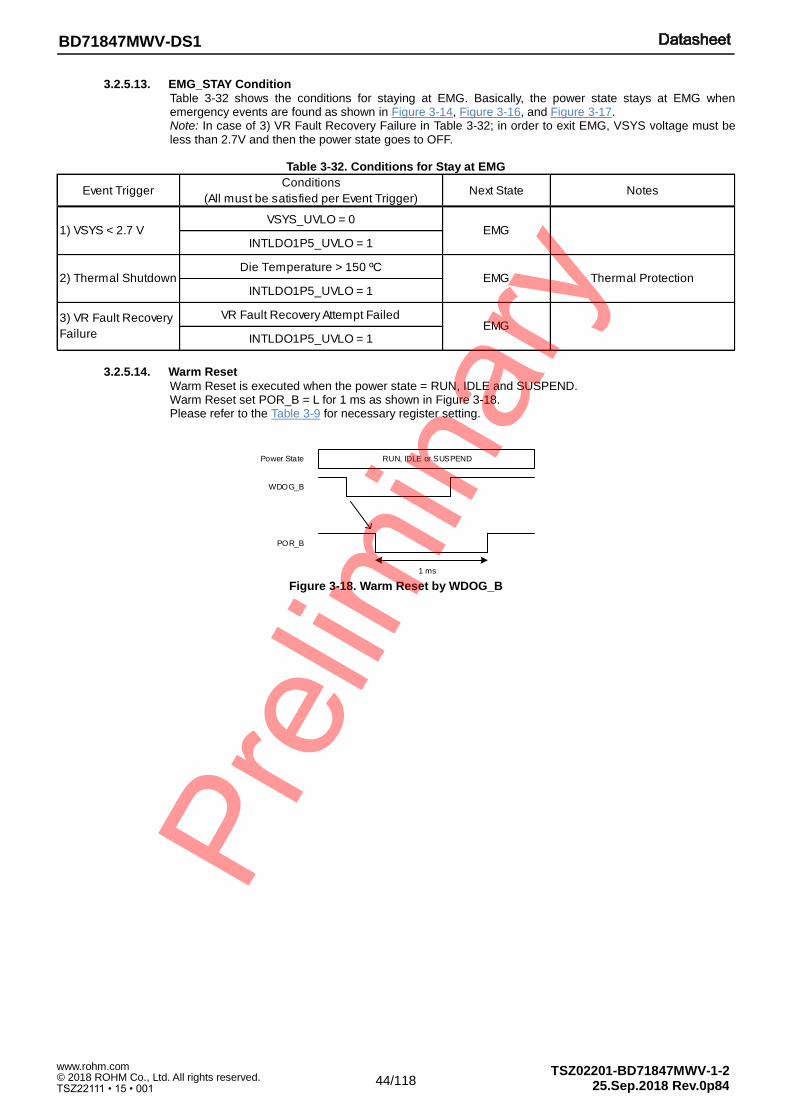
44/118 25.Sep.2018 Rev.0p84 © 2018 ROHM Co., Ltd. All rights reserved. www.rohm.com
TSZ22111 • 15 • 001
BD71847MWV-DS1
TSZ02201-BD71847MWV-1-2
3.2.5.13. EMG_STAY Condition
Table 3-32 shows the conditions for staying at EMG. Basically, the power state stays at EMG when emergency events are found as shown in Figure 3-14, Figure 3-16, and Figure 3-17. Note: In case of 3) VR Fault Recovery Failure in Table 3-32; in order to exit EMG, VSYS voltage must be less than 2.7V and then the power state goes to OFF.
Table 3-32. Conditions for Stay at EMG
3.2.5.14. Warm Reset
Warm Reset is executed when the power state = RUN, IDLE and SUSPEND. Warm Reset set POR_B = L for 1 ms as shown in Figure 3-18. Please refer to the Table 3-9 for necessary register setting.
Figure 3-18. Warm Reset by WDOG_B
Event TriggerConditions
(All must be satisfied per Event Trigger)Next State Notes
VSYS_UVLO = 0
INTLDO1P5_UVLO = 1
Die Temperature > 150 ºC
INTLDO1P5_UVLO = 1
VR Fault Recovery Attempt Failed
INTLDO1P5_UVLO = 1
1) VSYS < 2.7 V
2) Thermal Shutdown EMG Thermal Protection
3) VR Fault Recovery
FailureEMG
EMG
WDOG_B
Power State RUN, IDLE or SUSPEND
POR_B
1 ms
45/118 25.Sep.2018 Rev.0p84 © 2018 ROHM Co., Ltd. All rights reserved. www.rohm.com
TSZ22111 • 15 • 001
BD71847MWV-DS1
TSZ02201-BD71847MWV-1-2
3.2.5.15. PWROFF
Table 3-33 shows the conditions for shifting from RUN, IDLE, SUSPEND to PWROFF. When the power state is PWROFF, BD71847MWV runs Power OFF sequence and VR’s are turned OFF in a defined sequential order. In the end of the sequence, the on-off state of C32K_OUT, RTC_RESET_B, LDO2 and LDO1 depends on the setting of TRANS_COND1 register as shown in Table 3-34. The summary is shown in Table 3-35.
Table 3-33. Conditions from RUN, IDLE, SUSPEND to PWROFF
Table 3-34. TRANS_COND1 - Transition Condition Select 1 Register
Event TriggerConditions
(All must be satisfied per Event Trigger)Next State Notes
1) PWRON_B Long
PushPWRON_B = 0 ==> Long Push Detection PWROFF COLD_RESET event
2) WDOG_B WDOG_B = 0 PWROFF COLD_RESET event
3) Software Reset Write 1 to SWRESET in SWRESET register PWROFF COLD_RESET event
4) PMIC_ON_REQ PMIC_ON_REQ = 0 PWROFF
(Note) Die Temperature must be less than 150 ºC. VSYS_UVLO = 1.
Register Name R/W D7 D6 D5 D4 D3 D2 D1 D0 Initial Address
TRANS_COND1 R/W
PWRON_
POFF_TO_
READY
WDOG_
POFF_TO_
READY
SWRST_
POFF_TO_
READY
ON_REQ_
POFF_TO_
READY
0xC0 0x20
Bit
D[7:4]
D[3]
D[2]
D[1]
D[0]
Name Function Initial
PWRON_
POFF_TO_READY
Set which power state to go after PWROFF triggered by PWRON_B Long Push
0 = to SNVS
1 = to READY
0
PONT[3:0]
COLD RESET duration during which the BD71847MWV stays in READY or SNVS in
a COLD RESET event.
The BD71847MWV remains in READY or SNVS for the duration programmed here
then BD71847MWV performs a Power ON sequence.
0000 = 5 ms
0001 = 10 ms
0010 = 15 ms
0011 = 20 ms
0100 = 25 ms
0101 = 30 ms
0110 = 35 ms
0111 = 40 ms
1000 = 45 ms
1001 = 50 ms
1010 = 75 ms
1011 = 100 ms
1100 = 250 ms
1101 = 500 ms
1110 = 750 ms
1111 = 1500 ms
1100
WDOG_
POFF_TO_READY
Set which power state to go after PWROFF triggered by WDOG_B = 0
0 = to SNVS
1 = to READY
0
Set which power state to go after PWROFF triggered by Software Reset
0 = to SNVS
1 = to READY
0
PONT[3:0]
SWRST_
POFF_TO_READY
ON_REQ_
POFF_TO_READY
Set which power state to go after PWROFF triggered by PMIC_ON_REQ = 0
0 = to SNVS
1 = to READY
0

46/118 25.Sep.2018 Rev.0p84 © 2018 ROHM Co., Ltd. All rights reserved. www.rohm.com
TSZ22111 • 15 • 001
BD71847MWV-DS1
TSZ02201-BD71847MWV-1-2
3.2.5.15. PWROFF – continued
Figure 3-19. Cold Reset Duration Time set by PONT[3:0]
Table 3-35. VR Summary After Power OFF Sequence
VSYS
VRs
PONT[3:0] in
TRANS_COND1 register
more than 3.0 V
Power State PWROFF
(Power Off Sequence)
SNVS/
READY
SNVS/READY
(POW_SUB[1:0]=11)
RUN/SNVS
(Power On Sequence)
PWROFF trigger
PWRON_
POFF_TO_
READY
WDOG_
POFF_TO_
READY
SWRST_
POFF_TO_
READY
ON_REQ_
POFF_TO_
READY
C32K_
OUT
RTC_
RESET_BLDO2 LDO1
0 - - - On High On On
1 - - - Off Low Off Off
- 0 - - On High On On
- 1 - - Off Low Off Off
- - 0 - On High On On
- - 1 - Off Low Off Off
- - - 0 On High On On
- - - 1 Off Low Off Off
PWRON_B Long Push
WDOG_B = 0
Software Reset
PMIC_ON_REQ = 0

47/118 25.Sep.2018 Rev.0p84 © 2018 ROHM Co., Ltd. All rights reserved. www.rohm.com
TSZ22111 • 15 • 001
BD71847MWV-DS1
TSZ02201-BD71847MWV-1-2
3.2.5.16. PWROFF to READY
After the completion of Power OFF sequence, the power state goes READY if the POFF_TO_READY = 1. This is in accordance with PWROFF trigger event in the TRANS_COND1 register.
3.2.5.17. PWROFF to SNVS
After the completion of Power OFF sequence, the power state goes SNVS if the POFF_TO_READY = 0. This is in accordance with PWROFF trigger event in the TRANS_COND1 register.
3.2.5.18. PWRON_B Functionality
The system has a button that can be used for triggering the system to power on or off. PWRON_B is an active-low input to BD71847MWV. Timer circuitry measures the length of time the button is pressed. Then the timer detects short push and long push events.
Figure 3-20. Power Button Block Diagram
Table 3-36. PWRONCONFIG0 - PWRON_B Configuration 0 Register
BD71847MWV
PWRON_B
Power Button
VSYS
DebouncerEdge
DetectorTimer
Short Push
Long PushPowerState
Machine
IRQControl
IRQ_B
STAT_PWRON
IN_MON
PBDBNCT LONGTPWRONCONFIG0 SHORTT PWRONCONFIG1
Register Name R/W D7 D6 D5 D4 D3 D2 D1 D0 Initial Address
PWRONCONFIG0 R/W - - 0x16 0x27
Bit
D[5:4]
D[3:0]
Name Function Initial
PBDBNCT[1:0]PWRON_B Input Pin Debounce Time
00 = 10 ms 01 = 30 ms(default) 10 = 60 ms 11 = 100 ms01
PBDBNCT[1:0] SHORTT[3:0]
SHORTT[3:0]
Short Push Timer :
0000 = 10 ms
0001 = 0.5 s
0010 = 1.0 s
0011 = 1.5 s
0100 = 2.0 s
0101 = 2.5 s
0110 = 3.0 s (default)
0111 = 3.5 s
1000 = 4.0 s
1001 = 4.5 s
1010 = 5.0 s
1011 = 5.5 s
1100 = 6.0 s
1101 = 6.5 s
1110 = 7.0 s
1111 = 7.5 s
0110
48/118 25.Sep.2018 Rev.0p84 © 2018 ROHM Co., Ltd. All rights reserved. www.rohm.com
TSZ22111 • 15 • 001
BD71847MWV-DS1
TSZ02201-BD71847MWV-1-2
3.2.5.18. PWRON_B Functionality – continued Table 3-37. PWRONCONFIG1 - PWRON_B Configuration 1 Register
Register Name R/W D7 D6 D5 D4 D3 D2 D1 D0 Initial Address
PWRONCONFIG1 R/W - - - - 0x00 0x28
Bit
D[3:0]
LONGT[3:0]
Name Function Initial
LONGT[3:0]
Long Push Timer :
0000 = 10 ms (default)
0001 = 1 s
0010 = 2 s
0011 = 3 s
0100 = 4 s
0101 = 5 s
0110 = 6 s
0111 = 7 s
1000 = 8 s
1001 = 9 s
1010 = 10 s
1011 = 11 s
1100 = 12 s
1101 = 13 s
1110 = 14 s
1111 = 15 s
0000

49/118 25.Sep.2018 Rev.0p84 © 2018 ROHM Co., Ltd. All rights reserved. www.rohm.com
TSZ22111 • 15 • 001
BD71847MWV-DS1
TSZ02201-BD71847MWV-1-2
3.3. Power Sequence 3.3.1. Power ON Sequence
Figure 3-21 shows an example when TRANS_COND0 = 0x48, which are: READY to SNVS condition : VSYS_UVLO = 1 SNVS to RUN condition : PMIC_ON_REQ
Figure 3-21. Power ON Sequence
VSYS0 V
INTLD1P50 V
BUCK2 (0.9 V)
(VDD_ARM)
Power State OFF RUN
VSYS_UVLO
(PMIC Internal)
LDO1 (1.8 V)
(NVCC_SNVS)
RTC_RESET_B
(PMIC -> SOC)
POR_B
(PMIC -> SOC)
SNVS
Masked to H
PMIC_ON_REQ
(SOC -> PMIC)
LDO4 (0.9 V)
(VDDA_0V9)
BUCK5 (0.9 V)
(VDD_GPU,VDD_VPU,VDD_DRAM)
BUCK1 (0.8 V)
(VDD_SOC,VDDA_0V8,PHY_0V8)
LDO2 (0.8 V)
(VDD_SNVS)
RTC clock
(PMIC Internal) Stop
PMIC_STBY_REQ
(SOC -> PMIC) L
Stop
C32K_OUT
(PMIC -> SOC)
WDOG_B
(SOC -> PMIC)
LDO3 (1.8 V)
(VDDA_1V8)
BUCK6 (3.3 V)
(NVCC_3V3)
BUCK7 (1.8 V)
(NVCC_1V8)
BUCK8 (1.1 V)
(NVCC_DRAM)
LDO5 (3.3 V)
LDO6 (1.2 V)
(VDDA_1V2)
LDO5 is turned on by Software
Masked to L
3.0 V
Masked to L
READY
t0
t1
t2
t3
t4
t5
t6
t7
t8
t9
t10
t11
t12
t13
t14
t15

50/118 25.Sep.2018 Rev.0p84 © 2018 ROHM Co., Ltd. All rights reserved. www.rohm.com
TSZ22111 • 15 • 001
BD71847MWV-DS1
TSZ02201-BD71847MWV-1-2
3.3.1. Power ON Sequence – continued Table 3-38. Power ON Sequence Timing Specification
Symbol Description Min Typ Max Unit
t0 VSYS = 3.0 V to LDO1 Assert Delay 0 20 22 ms
t1 LDO1 Assert to LDO2 Assert Delay 0 2.0 2.4 ms
t2 LDO2 Assert to RTC_RESET_B De-assert Delay 0 10 12 ms
t3 RTC_RESET_B De-assert to C32K_OUT Output Delay 0 40 90 μs
t4 PMIC_ON_REQ Assert to BUCK1 Assert Delay 0 200 400 μs
t5 BUCK1 Assert to BUCK5 Assert Delay 0 2.0 2.4 ms
t6 BUCK1 Assert to LDO4 Assert Delay 0 2.0 2.4 ms
t7 LDO4 Assert to BUCK2 Assert Delay 0 2.0 2.4 ms
t8 LDO4 Assert to LDO3 Assert Delay 0 2.0 2.4 ms
t9 LDO3 Assert to BUCK7 Assert Delay 0 2.0 2.4 ms
t10 BUCK7 Assert to BUCK8 Assert Delay 0 2.0 2.4 ms
t11 BUCK8 Assert to BUCK6 Assert Delay 0 2.0 2.4 ms
t12 BUCK6 Assert to LDO6 Assert Delay 0 2.0 2.4 ms
t13 LDO6 Assert to POR_B De-assert Delay 0 20 22 ms
t14 POR_B De-assert to WDOG_B Internal Mask Disabled 0 10 12 ms
t15
POR_B De-assert to PMIC_STBY_REQ Internal Mask
Disabled0 10 12 ms

51/118 25.Sep.2018 Rev.0p84 © 2018 ROHM Co., Ltd. All rights reserved. www.rohm.com
TSZ22111 • 15 • 001
BD71847MWV-DS1
TSZ02201-BD71847MWV-1-2
3.3.2. Power OFF Sequence
Figure 3-22 shows an example when triggered by PMIC_ON_REQ when ON_REQ_POFF_TO_READY = 0 in TRANS_COND1 register.
Figure 3-22. Power OFF Sequence (To SNVS)
VSYS
INTLDO1P5
Power State RUN
VSYS_UVLO
(PMIC Internal)
LDO1 (1.8 V)
(NVCC_SNVS)
POR_B
(PMIC -> SOC)
SNVS
Masked to H
PMIC_ON_REQ
(SOC -> PMIC)
BUCK1 (0.8 V)
(VDD_SOC,VDDA_0V8,PHY_0V8)
LDO2 (0.8 V)
(VDD_SNVS)
RTC clock
(PMIC Internal)
PMIC_STBY_REQ
(SOC -> PMIC)
WDOG_B
(SOC -> PMIC)
LDO5 (3.3 V)
LDO6 (1.2 V)
(VDDA_1V2)
H
H
H
L
0.8 V
1.8 V
PWROFF
RTC_RESET_B
(PMIC -> SOC)
C32K_OUT
(PMIC -> SOC)
BUCK2 (0.9 V)
(VDD_ARM)
LDO4 (0.9 V)
(VDDA_0V9)
BUCK5 (0.9 V)
(VDD_GPU,VDD_VPU,VDD_DRAM)
LDO3 (1.8 V)
(VDDA_1V8)
BUCK6 (3.3 V)
(NVCC_3V3)
BUCK7 (1.8 V)
(NVCC_1V8)
BUCK8 (1.1 V)
(NVCC_DRAM)
t0
t1
t2
t3
t4
t5
t6
t7
t8
t9
t10

52/118 25.Sep.2018 Rev.0p84 © 2018 ROHM Co., Ltd. All rights reserved. www.rohm.com
TSZ22111 • 15 • 001
BD71847MWV-DS1
TSZ02201-BD71847MWV-1-2
3.3.2. Power OFF Sequence – continued Table 3-39. Power OFF Sequence Timing Specification (To SNVS)
Symbol Description Min Typ Max Unit
t0 PMIC_ON_REQ De-assert to POR_B Assert Delay 0 120 200 μs
t1 POR_B De-assert to LDO5 De-assert Delay 0 10 12 ms
t2 LDO5 De-assert to LDO6 De-assert Delay 0 30 35 ms
t3 LDO6 De-assert to BUCK6 De-assert Delay 0 10 12 ms
t4 BUCK6 De-assert to BUCK8 De-assert Delay 0 10 12 ms
t5 BUCK8 De-assert to BUCK7 De-assert Delay 0 10 12 ms
t6 BUCK7 De-assert to LDO3 De-assert Delay 0 10 12 ms
t7 LDO3 De-assert to BUCK2 De-assert Delay 0 10 12 ms
t8 BUCK2 De-assert to LDO4 De-assert Delay 0 10 12 ms
t9 LDO4 De-assert to BUCK5 De-assert delay 0 10 12 ms
t10 BUCK5 De-assert to BUCK1 De-assert Delay 0 10 12 ms

53/118 25.Sep.2018 Rev.0p84 © 2018 ROHM Co., Ltd. All rights reserved. www.rohm.com
TSZ22111 • 15 • 001
BD71847MWV-DS1
TSZ02201-BD71847MWV-1-2
3.3.2. Power OFF Sequence – continued
Figure 3-23 shows an example when triggered by PMIC_ON_REQ when ON_REQ_POFF_TO_READY = 1 in TRANS_COND1 register.
Figure 3-23. Power OFF Sequence (To READY)
VSYS
INTLDO1P5
Power State RUN
VSYS_UVLO
(PMIC Internal)
LDO1 (1.8 V)
(NVCC_SNVS)
POR_B
(PMIC -> SOC)
READY
Masked to H
PMIC_ON_REQ
(SOC -> PMIC)
LDO2 (0.8 V)
(VDD_SNVS)
RTC clock
(PMIC Internal)
PMIC_STBY_REQ
(SOC -> PMIC)
WDOG_B
(SOC -> PMIC)
H
H
H
L
0.8 V
1.8 V
PWROFF
RTC_RESET_B
(PMIC -> SOC)
C32K_OUT
(PMIC -> SOC)
BUCK1 (0.8 V)
(VDD_SOC,VDDA_0V8,PHY_0V8)
LDO5 (3.3 V)
LDO6 (1.2 V)
(VDDA_1V2)
BUCK2 (0.9 V)
(VDD_ARM)
LDO4 (0.9 V)
(VDDA_0V9)
BUCK5 (0.9 V)
(VDD_GPU,VDD_VPU,VDD_DRAM)
LDO3 (1.8 V)
(VDDA_1V8)
BUCK6 (3.3 V)
(NVCC_3V3)
BUCK7 (1.8 V)
(NVCC_1V8)
BUCK8 (1.1 V)
(NVCC_DRAM)
t0
t1
t2
t3
t4
t5
t6
t7
t8
t9
t10
t11
t12
t13
t14

54/118 25.Sep.2018 Rev.0p84 © 2018 ROHM Co., Ltd. All rights reserved. www.rohm.com
TSZ22111 • 15 • 001
BD71847MWV-DS1
TSZ02201-BD71847MWV-1-2
3.3.2. Power OFF Sequence – continued Table 3-40. Power OFF Sequence Timing Specification (To READY)
Symbol Description Min Typ Max Unit
t0 PMIC_ON_REQ De-assert to POR_B Assert Delay 0 120 200 μs
t1 POR_B Assert to LDO5 De-assert Delay 0 10 12 ms
t2 LDO5 De-assert to LDO6 De-assert Delay 0 30 35 ms
t3 LDO6 De-assert to BUCK6 De-assert Delay 0 10 12 ms
t4 BUCK6 De-assert to BUCK8 De-assert Delay 0 10 12 ms
t5 BUCK8 De-assert to BUCK7 De-assert Delay 0 10 12 ms
t6 BUCK7 De-assert to LDO3 De-assert Delay 0 10 12 ms
t7 LDO3 De-assert to BUCK2 De-assert Delay 0 10 12 ms
t8 BUCK2 De-assert to LDO4 De-assert Delay 0 10 12 ms
t9 LDO4 De-assert to BUCK5 De-assert Delay 0 10 12 ms
t10 BUCK5 De-assert to BUCK1 De-assert Delay 0 10 12 ms
t11 BUCK1 De-assert to C32K_OUT Output Stop Delay 0 10 12 ms
t12 C32K_OUT Output Stop to RTC_RESET_B Assert Delay 0 10 12 ms
t13 RTC_RESET_B Assert to LDO2 De-assert Delay 0 10 12 ms
t14 LDO2 De-assert to LDO1 De-assert Delay 0 10 12 ms

55/118 25.Sep.2018 Rev.0p84 © 2018 ROHM Co., Ltd. All rights reserved. www.rohm.com
TSZ22111 • 15 • 001
BD71847MWV-DS1
TSZ02201-BD71847MWV-1-2
3.3.3. RUN to IDLE
Figure 3-24. RUN to IDLE
Table 3-41. RUN to IDLE Timing Specification
Power State RUN
LDO1 (1.8 V)
(NVCC_SNVS)
RTC_RESET_B
(PMIC -> SOC)
POR_B
(PMIC -> SOC)
IDLE
PMIC_ON_REQ
(SOC -> PMIC)
LDO2 (0.8 V)
(VDD_SNVS)
RTC clock
(PMIC Internal)
PMIC_STBY_REQ
(SOC -> PMIC)
C32K_OUT
(PMIC -> SOC)
WDOG_B
(SOC -> PMIC)
H
H
L
0.8 V
1.8 V
H
H
I2C Interface
(SOC -> PMIC)Write 1 to IDLE_MODE in
PWRCTRL1 register
0.8 V
1.2 V
0.9 V
3.3 V
1.8 V
0.9 V
0.9 V
3.3 V
Voltage specified by BUCK2_VOLT_IDLE[5:0]
Voltage specified by BUCK1_VOLT_IDLE[5:0]
1.1 V
1.8 V
BUCK1 (0.8 V)
(VDD_SOC,VDDA_0V8,PHY_0V8)
LDO5 (3.3 V)
LDO6 (1.2 V)
(VDDA_1V2)
BUCK2 (0.9 V)
(VDD_ARM)
LDO4 (0.9 V)
(VDDA_0V9)
BUCK5 (0.9 V)
(VDD_GPU,VDD_VPU,VDD_DRAM)
LDO3 (1.8 V)
(VDDA_1V8)
Voltage specified by BUCK2_VOLT_RUN[5:0]
BUCK6 (3.3 V)
(NVCC_3V3)
BUCK7 (1.8 V)
(NVCC_1V8)
BUCK8 (1.1 V)
(NVCC_DRAM)
t0
t1
Symbol Description Min Typ Max Unit
t0 End of I2C Access to BUCK2 Voltage Change Start 0 120 200 μs
t1 BUCK2 to BUCK1 Voltage Change Delay 0 120 200 μs

56/118 25.Sep.2018 Rev.0p84 © 2018 ROHM Co., Ltd. All rights reserved. www.rohm.com
TSZ22111 • 15 • 001
BD71847MWV-DS1
TSZ02201-BD71847MWV-1-2
3.3.4. IDLE to RUN
Figure 3-25. IDLE to RUN
Table 3-42. IDLE to RUN Timing Specification
Power State IDLE
LDO1 (1.8 V)
(NVCC_SNVS)
RTC_RESET_B
(PMIC -> SOC)
POR_B
(PMIC -> SOC)
RUN
PMIC_ON_REQ
(SOC -> PMIC)
LDO2 (0.8 V)
(VDD_SNVS)
RTC clock
(PMIC Internal)
PMIC_STBY_REQ
(SOC -> PMIC)
C32K_OUT
(PMIC -> SOC)
WDOG_B
(SOC -> PMIC)
H
H
H
0.8 V
1.8 V
H
H
I2C Interface
(SOC -> PMIC)Write 0 to IDLE_MODE in
PWRCTRL1 register
0.8V = Voltage specified by BUCK1_VOLT_RUN[5:0]
0.9V = Voltage specified by BUCK2_VOLT_RUN[5:0]
3.3 V
0.9 V
Voltage specified by BUCK2_VOLT_IDLE[5:0]
Voltage specified by BUCK1_VOLT_IDLE[5:0]
1.2 V
3.3 V
1.8 V
0.9 V
1.1 V
BUCK5 (0.9 V)
(VDD_GPU,VDD_VPU,VDD_DRAM)
BUCK1 (0.8 V)
(VDD_SOC,VDDA_0V8,PHY_0V8)
1.8 V
LDO5 (3.3 V)
LDO6 (1.2 V)
(VDDA_1V2)
BUCK2 (0.9 V)
(VDD_ARM)
LDO4 (0.9 V)
(VDDA_0V9)
LDO3 (1.8 V)
(VDDA_1V8)
BUCK6 (3.3 V)
(NVCC_3V3)
BUCK7 (1.8 V)
(NVCC_1V8)
BUCK8 (1.1 V)
(NVCC_DRAM)
t0
t1
Symbol Description Min Typ Max Unit
t0 End of I2C Access to BUCK1 Voltage Change Start 0 120 200 μs
t1 BUCK1 to BUCK2 Voltage Change Delay 0 120 200 μs

57/118 25.Sep.2018 Rev.0p84 © 2018 ROHM Co., Ltd. All rights reserved. www.rohm.com
TSZ22111 • 15 • 001
BD71847MWV-DS1
TSZ02201-BD71847MWV-1-2
3.3.5. RUN to SUSPEND
Figure 3-26. RUN to SUSPEND
Table 3-43. RUN to SUSPEND Timing Specification
Power State RUN
LDO1 (1.8 V)
(NVCC_SNVS)
RTC_RESET_B
(PMIC -> SOC)
POR_B
(PMIC -> SOC)
SUSPEND
PMIC_ON_REQ
(SOC -> PMIC)
RTC clock
(PMIC Internal)
PMIC_STBY_REQ
(SOC -> PMIC)
C32K_OUT
(PMIC -> SOC)
WDOG_B
(SOC -> PMIC)
H
H
H
0.8 V
1.8 V
H
H
0.8 V
0.9 V
3.3 V
1.8 V
Voltage specified by BUCK1_VOLT_SUSP[5:0]
1.2 V
0.9 V
3.3 V
1.8 V
0.9 V
1.1 V
BUCK5 (0.9 V)
(VDD_GPU,VDD_VPU,VDD_DRAM)
BUCK1 (0.8 V)
(VDD_SOC,VDDA_0V8,PHY_0V8)
LDO2 (0.8 V)
(VDD_SNVS)
LDO5 (3.3 V)
LDO6 (1.2 V)
(VDDA_1V2)
BUCK2 (0.9 V)
(VDD_ARM)
LDO4 (0.9 V)
(VDDA_0V9)
LDO3 (1.8 V)
(VDDA_1V8)
0 V (OFF)
BUCK6 (3.3 V)
(NVCC_3V3)
BUCK7 (1.8 V)
(NVCC_1V8)
BUCK8 (1.1 V)
(NVCC_DRAM)
t0
t2
t1 0 V (OFF)
Symbol Description Min Typ Max Unit
t0 PMIC_STBY_REQ High to BUCK2 De-assert Delay 0 120 200 μs
t1 BUCK2 to BUCK5 Voltage Change Delay 0 10 12 ms
t2 BUCK5 to BUCK1 Voltage Change Delay 0 10 12 ms

58/118 25.Sep.2018 Rev.0p84 © 2018 ROHM Co., Ltd. All rights reserved. www.rohm.com
TSZ22111 • 15 • 001
BD71847MWV-DS1
TSZ02201-BD71847MWV-1-2
3.3.6. SUSPEND to RUN
Figure 3-27. SUSPEND to RUN
Table 3-44. SUSPEND to RUN Timing Specification
Power State SUSPEND
LDO1 (1.8 V)
(NVCC_SNVS)
RTC_RESET_B
(PMIC -> SOC)
POR_B
(PMIC -> SOC)
RUN
PMIC_ON_REQ
(SOC -> PMIC)
LDO2 (0.8 V)
(VDD_SNVS)
RTC clock
(PMIC Internal)
PMIC_STBY_REQ
(SOC -> PMIC)
C32K_OUT
(PMIC -> SOC)
WDOG_B
(SOC -> PMIC)
H
H
H
0.8 V
1.8 V
H
H
Voltage specified by BUCK1_VOLT_RUN[5:0]
3.3 V
1.8 V
Voltage specified by BUCK1_VOLT_SUSP[5:0]
0 V (OFF)
1.2 V
3.3 V
1.8 V
0.9 V
1.1 V
BUCK5 (0.9 V)
(VDD_GPU,VDD_VPU,VDD_DRAM)
BUCK1 (0.8 V)
(VDD_SOC,VDDA_0V8,PHY_0V8)
LDO5 (3.3 V)
LDO6 (1.2 V)
(VDDA_1V2)
BUCK2 (0.9 V)
(VDD_ARM)
LDO4 (0.9 V)
(VDDA_0V9)
LDO3 (1.8 V)
(VDDA_1V8)
BUCK6 (3.3 V)
(NVCC_3V3)
BUCK7 (1.8 V)
(NVCC_1V8)
BUCK8 (1.1 V)
(NVCC_DRAM)
t0
t1
t2
0 V (OFF)
0.9 V
0.9 V
Symbol Description Min Typ Max Unit
t0 PMIC_STBY_REQ Low to BUCK1 Voltage Change Start 0 120 200 μs
t1 BUCK1 to BUCK5 Voltage Change Delay 0 1.0 1.2 ms
t2 BUCK5 to BUCK2 Voltage Change Delay 0 1.0 1.2 ms
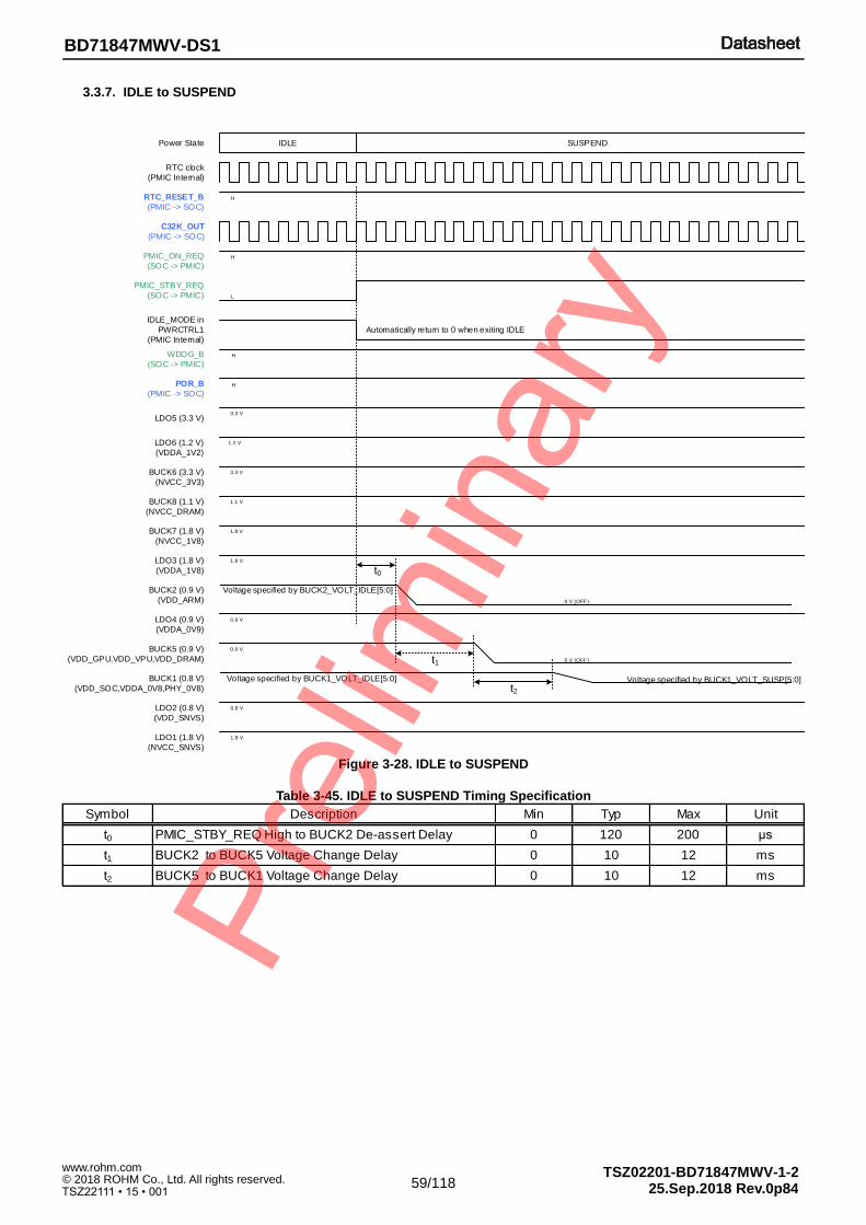
59/118 25.Sep.2018 Rev.0p84 © 2018 ROHM Co., Ltd. All rights reserved. www.rohm.com
TSZ22111 • 15 • 001
BD71847MWV-DS1
TSZ02201-BD71847MWV-1-2
3.3.7. IDLE to SUSPEND
Figure 3-28. IDLE to SUSPEND
Table 3-45. IDLE to SUSPEND Timing Specification
Power State IDLE
LDO1 (1.8 V)
(NVCC_SNVS)
RTC_RESET_B
(PMIC -> SOC)
POR_B
(PMIC -> SOC)
SUSPEND
PMIC_ON_REQ
(SOC -> PMIC)
LDO2 (0.8 V)
(VDD_SNVS)
RTC clock
(PMIC Internal)
PMIC_STBY_REQ
(SOC -> PMIC)
C32K_OUT
(PMIC -> SOC)
WDOG_B
(SOC -> PMIC)
H
H
L
0.8 V
1.8 V
H
H
0.9 V
0.9 V
3.3 V
1.8 V
1.1 V
1.2 V
3.3 V
1.8 V
IDLE_MODE in
PWRCTRL1
(PMIC Internal)
Automatically return to 0 when exiting IDLE
BUCK5 (0.9 V)
(VDD_GPU,VDD_VPU,VDD_DRAM)
BUCK1 (0.8 V)
(VDD_SOC,VDDA_0V8,PHY_0V8)
LDO5 (3.3 V)
LDO6 (1.2 V)
(VDDA_1V2)
BUCK2 (0.9 V)
(VDD_ARM)
LDO4 (0.9 V)
(VDDA_0V9)
LDO3 (1.8 V)
(VDDA_1V8)
BUCK6 (3.3 V)
(NVCC_3V3)
BUCK7 (1.8 V)
(NVCC_1V8)
BUCK8 (1.1 V)
(NVCC_DRAM)
t0
t1
t2Voltage specified by BUCK1_VOLT_SUSP[5:0]
0 V (OFF)
Voltage specified by BUCK2_VOLT_IDLE[5:0]
Voltage specified by BUCK1_VOLT_IDLE[5:0]
0 V (OFF)
Symbol Description Min Typ Max Unit
t0 PMIC_STBY_REQ High to BUCK2 De-assert Delay 0 120 200 μs
t1 BUCK2 to BUCK5 Voltage Change Delay 0 10 12 ms
t2 BUCK5 to BUCK1 Voltage Change Delay 0 10 12 ms

60/118 25.Sep.2018 Rev.0p84 © 2018 ROHM Co., Ltd. All rights reserved. www.rohm.com
TSZ22111 • 15 • 001
BD71847MWV-DS1
TSZ02201-BD71847MWV-1-2
3.3.8. Emergency Shutdown
Figure 3-29. Emergency Shutdown
Table 3-46. Emergency Shutdown Timing Specification
VSYS
INTLDO1P5
Power State Any State except OFF and READY
VSYS_UVLO
(PMIC Internal)
LDO1 (1.8 V)
(NVCC_SNVS)
RTC_RESET_B
(PMIC -> SOC)
POR_B
(PMIC -> SOC)
EMG
LDO2 (0.8 V)
(VDD_SNVS)
RTC clock
(PMIC Internal)
C32K_OUT
(PMIC -> SOC)
H
H
H
Emergency
Event
Thermal Shutdown Event occurs .
When Power S tate = SNVS
When Power S tate = RUN, IDLE and SUSPEND
BUCK5 (0.9 V)
(VDD_GPU,VDD_VPU,VDD_DRAM)
BUCK1 (0.8 V)
(VDD_SOC,VDDA_0V8,PHY_0V8)
LDO5 (3.3 V)
LDO6 (1.2 V)
(VDDA_1V2)
BUCK2 (0.9 V)
(VDD_ARM)
LDO4 (0.9 V)
(VDDA_0V9)
LDO3 (1.8 V)
(VDDA_1V8)
BUCK6 (3.3 V)
(NVCC_3V3)
BUCK7 (1.8 V)
(NVCC_1V8)
BUCK8 (1.1 V)
(NVCC_DRAM)
t0
t1
Symbol Description Min Typ Max Unit
t0Emergency Event to POR_B Assert and
All VRs Except BUCK7 De-assert Delay0 120 200 μs
t1 POR_B Assert to BUCK7 De-assert Delay 0 30 35 ms

61/118 25.Sep.2018 Rev.0p84 © 2018 ROHM Co., Ltd. All rights reserved. www.rohm.com
TSZ22111 • 15 • 001
BD71847MWV-DS1
TSZ02201-BD71847MWV-1-2
3.3.9. Warm Reset
Figure 3-30. Warm Reset (SWRESET)
Table 3-47. Warm Reset (SWRESET) Timing Specification
Figure 3-31. Warm Reset (WDOG_B)
Table 3-48. Warm Reset (WDOG_B) Timing Specification
Figure 3-32. Warm Reset (PWRON_B Long Push)
Table 3-49. Warm Reset (PWRON_B Long Push) Timing Specification
SCL
POR_B
SDA
I2C Write Access for SWRESET = 1
D0
STOP
ACK
t0
t1
Symbol Description Min Typ Max Unit
t0 SCL rising to POR_B assert delay - - 1.0 μs
t1 POR_B assert duration time 0.95 1.00 1.05 ms
POR_B
WDOG_BIncluding debounce time = 100μs
t0
t1
Symbol Description Min Typ Max Unit
t0 WDOG_B falling to POR_B assert delay 100 110 120 μs
t1 POR_B assert duration time 0.95 1.00 1.05 ms
POR_B
PWRON_B
t0
t1
Symbol Description Min Typ Max Unit
t0 PWRON_B falling to POR_B assert delay
PBDBNCT[1:0] in
PWRONCONFIG0
+ LONGT[3:0] in
PWRONCONFIG1
-50
PBDBNCT[1:0] in
PWRONCONFIG0
+ LONGT[3:0] in
PWRONCONFIG1
PBDBNCT[1:0] in
PWRONCONFIG0
+ LONGT[3:0] in
PWRONCONFIG1
+50
ms
t1 POR_B assert duration time 0.95 1.00 1.05 ms

62/118 25.Sep.2018 Rev.0p84 © 2018 ROHM Co., Ltd. All rights reserved. www.rohm.com
TSZ22111 • 15 • 001
BD71847MWV-DS1
TSZ02201-BD71847MWV-1-2
3.3.10. Reset Source Indicators The BD71847MWV has RESETSRC register which is intended to store the cause of a shutdown or reset, the firmware reads this data on the next startup. Depending on the cause of a shutdown or reset, the only bit of RESETSRC register is 1.
Table 3-50. RESETSRC - Reset Source Indicator Register
Register Name R/W D7 D6 D5 D4 D3 D2 D1 D0 Initial Address
RESETSRC R/W RPWRON RWDOG RSWRSTRPMIC_ON_
REQRVSYS_2P7 RTEMP ROCP RVR_FAULT 0x00 0x29
Bit
D[7]
D[6]
D[5]
D[4]
D[3]
D[2]
D[1]
D[0]
RTEMP
0 = Default
1 = Previous shutdown was due to the Emergency Thermal Shutdown
(Write-1-clear bit)
0
ROCP
0 = Default
1 = Previous shutdown was due to the Emergency OCP
(Write-1-clear bit)
0
RVR_FAULT
0 = Default
1 = Previous shutdown was due to the Emergency VR Fault
(Write-1-clear bit)
0
RPMIC_ON_REQ
0 = Default
1 = Previous shutdown was due to the PMIC_ON_REQ = 0
(Write-1-clear bit)
0
RVSYS_2P7
0 = Default
1 = Previous shutdown was due to the Emergency VSYS < 2.7V
(Write-1-clear bit)
0
RWDOG
0 = Default
1 = Previous shutdown was due to the WDOG_B Cold Reset
(Write-1-clear bit)
0
RSWRST
0 = Default
1 = Previous shutdown was due to the Software Cold Reset
(Write-1-clear bit)
0
Name Function Initial
RPWRON
0 = Default
1 = Previous shutdown was due to the PWRON_B Long Push Cold Reset
(Write-1-clear bit)
0

63/118 25.Sep.2018 Rev.0p84 © 2018 ROHM Co., Ltd. All rights reserved. www.rohm.com
TSZ22111 • 15 • 001
TSZ02201-BD71847MWV-1-2
BD71847MWV-DS1
4. I2C and Interrupt
4.1. I2C Bus Interface
4.1.1. I2C Bus Interface Overview
I2C access is not permitted when the power state = READY.
Figure 4-1. I2C (Slave) Block Diagram
DVDD
DVDD
DVDD
DVDD
SCL
SDA
Spike Filter
Spike Filter
[Internal Logic Circuit]
I2C slave controller
GND

64/118 25.Sep.2018 Rev.0p84 © 2018 ROHM Co., Ltd. All rights reserved. www.rohm.com
TSZ22111 • 15 • 001
TSZ02201-BD71847MWV-1-2
BD71847MWV-DS1
4.1.2. I2C Bus Interface Electrical Characteristics
Table 4-1. I2C Bus Interface DC Electrical Characteristics
Min Typ Max
SCL
Input "H" LevelVIH_SCL
DVDD
x 0.7-
DVDD
+ 0.3V
SCL
Input "L" LevelVIL_SCL -0.3 -
DVDD
x 0.3V
SCL
Input HysteresisVIHYS_SCL 0.1 - - V
SCL
Input Leak Current(Input=0 V)IOFF1_SCL -1 - +1 μA
SCL
Input Leak Current(Input=5.5 V)IOFF2_SCL -1 - +1 μA
SDA
Input "H" LevelVIH_SDA
DVDD
x 0.7-
DVDD
+ 0.3V
SDA
Input "L" LevelVIL_SDA -0.3 -
DVDD
x 0.3V
SDA
Input HysteresisVIHYS_SDA 0.1 - - V
SDA
Input Leak Current(Input=0 V)IOFF1_SDA -1 - +1 μA
SDA
Input Leak Current(Input=5.5 V)IOFF2_SDA -1 - +1 μA
SDA
Output "L" Level VoltageVOL_SDA - - 0.4 V IOL=6mA
Output Off Leak Current(Input=0
V)IOFF3_SDA -1 - +1 μA
Output Off Leak
Current(Input=5.5 V)IOFF4_SDA -1 - +1 μA
Digital pin characteristics – Input (SCL)
Digital pin characteristics – Input (SDA)
Digital pin characteristics - Output (SDA)
(Unless otherwise specified, Ta=+25°C, VSYS=5.0 V, DVDD=1.8 V)
Parameter SymbolLimit
Unit Condition

65/118 25.Sep.2018 Rev.0p84 © 2018 ROHM Co., Ltd. All rights reserved. www.rohm.com
TSZ22111 • 15 • 001
TSZ02201-BD71847MWV-1-2
BD71847MWV-DS1
4.1.2. I2C Bus Interface Electrical Characteristics – continued Table 4-2. I2C Bus Interface AC Timing - Fast Mode
Figure 4-2. I2C Bus Interface AC Timing
Min Typ Max Min Typ Max
I2C_CLK Clock Frequency fSCLH 0 - 400 0 - 1000 kHz
Hold Time START Condition tHD_STA 0.60 - - 0.26 - - μs
LOW Period of I2C_CLK Clock tLOW 1.3 - - 0.5 - - μs
HIGH Period of I2C_CLK Clock tHIGH 0.60 - - 0.26 - - μs
Set-up Time for a Repeated START
ConditiontSU_STA 0.60 - - 0.26 - - μs
Data Hold Time tHD_DAT 0 - - 0 - - ns
Data Set-up Time tSU_DAT 100 - - 50 - - ns
Set-up Time for STOP Condition tSU_STO 0.60 - - 0.26 - - μs
Fall Time of I2C_DATA Signal tFDA 20 300 - - 120 ns
Capacitive Load for Each Bus Line CB - - 400 - - 550 pF
Pulse Width of Spikes that are
Suppressed by the Input FiltertSP 0 - 50 0 - 50 ns
Bus Free Time tBUFF 1.3 0.5 - - μs
Data Valid Time tVD_DAT 0.90 - - 0.45 μs
Data Valid Acknowledge Time tVD_ACK 0.90 - - 0.45 μs
(Unless otherwise specified, Ta=+25°C, VSYS=5.0 V, DVDD=1.8 V)
UnitParameter SymbolFast mode Fast mode plus
70%
30%SDA
SCL
70%
30%
tF tSU_DAT
tVD_DAT
tHD_DAT
tHD_STA
1 / fSCL tLOW
tHIGHS
tHD_STAtSU_STA
70%
30%
70%
30%
tSP
tVD_ACK
tSU_STO
tBUF
P S
SDA
SCL
Sr
tR
tF
tR

66/118 25.Sep.2018 Rev.0p84 © 2018 ROHM Co., Ltd. All rights reserved. www.rohm.com
TSZ22111 • 15 • 001
TSZ02201-BD71847MWV-1-2
BD71847MWV-DS1
4.1.3. Device Addressing
Table 4-3. I2C_DEV - I2C Device Address Indicator Register
Figure 4-3. I2C Device Addressing
Register Name R/W D7 D6 D5 D4 D3 D2 D1 D0 Initial Address
I2C_DEV R - - - - - - 0x03 0x02
Bit
D[1:0]
I2C_DEV_ADRS[1:0]
Name Function Initial
I2C_DEV_ADRS[1:0]
00 = I2C Device Address lower 2bits = 00
01 = I2C Device Address lower 2bits = 01
10 = I2C Device Address lower 2bits = 10
11 = I2C Device Address lower 2bits = 11
11
1 0 0 1 0 0 0 R / W
MSB LSB
1 0 0 1 0 0 1 R / W
MSB LSB
1 0 0 1 0 1 0 R / W
MSB LSB
1 0 0 1 0 1 1 R / W a
MSB LSB
I2C Device Address is decided by OTP setting.
I2C Device Address Read / Write instruction bit

67/118 25.Sep.2018 Rev.0p84 © 2018 ROHM Co., Ltd. All rights reserved. www.rohm.com
TSZ22111 • 15 • 001
TSZ02201-BD71847MWV-1-2
BD71847MWV-DS1
4.1.4. Write / Read Operation
Figure 4-4. I2C Write / Read Operation
Write single register
S W Ack Ack Ack P
Write multiple registers (Address Auto-Increment)
S W Ack Ack Ack Ack
Ack Ack Ack Ack P
Read single register
S W Ack Ack Sr R Ack NAck P
Read multiple registers (Address Auto-Increment)
S W Ack Ack Sr R Ack Ack
Ack Ack Ack NAck P
S Start Condition Sr Repeat Start Condition P Stop Condition
W Write (= Low) R Read (= High)
Ack Acknowledge (= Low, driven by I2C Slave) Ack Acknowledge (= Low, driven by I2C Master)
NAck Not Acknowledge (= High, driven by I2C Master)
8-bit Data
(Write Data #1)
8-bit Data
(Write Data #2)
8-bit Data
(Write Data #3)
8-bit Data
(Write Data #N)
7-bit Device
Address
8-bit Data
(Reg. Address)
8-bit Data
(Write Data)
7-bit Device
Address
8-bit Data
(Reg. Address)
8-bit Data
(Write Data #1)
8-bit Data
(Read Data #2)
8-bit Data
(Read Data #3)
8-bit Data
(Read Data #N)
7-bit Device
Address
8-bit Data
(Reg. Address)
7-bit Device
Address
8-bit Data
(Read Data)
7-bit Device
Address
8-bit Data
(Reg. Address)
7-bit Device
Address
8-bit Data
(Read Data #1)

68/118 25.Sep.2018 Rev.0p84 © 2018 ROHM Co., Ltd. All rights reserved. www.rohm.com
TSZ22111 • 15 • 001
TSZ02201-BD71847MWV-1-2
BD71847MWV-DS1
4.2. Interrupt 4.2.1. Interrupt Overview
Table 4-4. Interrupt Event
Figure 4-5. IRQ_B Architecture Block Diagram
Table 4-5. IRQ_B Electrical Characteristics
IRQ Event Definition
PWRON PWRON_B Pin Level Changed
PWRON_S PWRON_B Short Push Detection
PWRON_L PWRON_B Long Push Detection
WDOG WDOG_B Pin Level Changed
SWRST Written 1 to SWRESET in SWRESET Register
ON_REQ PMIC_ON_REQ Pin Level Changed
STBY_REQ PMIC_STBY_REQ Pin Level Changed
D QRN
CPIRQ Event
Write 1 ClearMask bit from
MIRQ register
to IRQ register
IRQ_B
Min Typ Max
Output "L" Level Voltage VOL_IRQB - - DVDD x 0.2 V IOL=3 mA Sink
Output Off Leak Current IOLK_IRQB -1 - +1 μA
(Unless otherwise specified, Ta=+25°C, VSYS=5.0 V, DVDD=1.8 V)
Parameter SymbolLimit
Unit Condition

69/118 25.Sep.2018 Rev.0p84 © 2018 ROHM Co., Ltd. All rights reserved. www.rohm.com
TSZ22111 • 15 • 001
TSZ02201-BD71847MWV-1-2
BD71847MWV-DS1
4.2.1. Interrupt Overview – continued Table 4-6. IRQ - Interrupt Register
Table 4-7. MIRQ – IRQ Mask Register
Register Name R/W D7 D6 D5 D4 D3 D2 D1 D0 Initial Address
IRQ R/W - SWRST PWRON_S PWRON_L PWRON WDOG ON_REQ STBY_REQ 0x00 0x2B
Bit
D[6]
D[5]
D[4]
D[3]
D[2]
D[1]
D[0]
0
0
0
0
0
0 = PWRON_B Short Push not detected
1 = PWRON_B Short Push detected
This bit is a write-1-to-clear bit.
0 = PWRON_B Long Push not detected
1 = PWRON_B Long Push detected
This bit is a write-1-to-clear bit.
0 = PWRON_B level change not generated
1 = PWRON_B level change generated
This bit is a write-1-to-clear bit.
0 = WDOG_B level change not generated
1 = WDOG_B level change generated
This bit is a write-1-to-clear bit.
0 = PMIC_ON_REQ level change not generated
1 = PMIC_ON_REQ level change generated
This bit is a write-1-to-clear bit.
PWRON_S
PWRON_L
PWRON
WDOG
ON_REQ
Name InitialFunction
SWRST
0 = SWRESET in SWRESET register is not written 1
1 = SWRESET in SWRESET register is written 1
This bit is a write-1-to-clear bit.
0
STBY_REQ
0 = PMIC_STBY_REQ level change not generated
1 = PMIC_STBY_REQ level change generated
This bit is a write-1-to-clear bit.
0
Register Name R/W D7 D6 D5 D4 D3 D2 D1 D0 Initial Address
MIRQ R/W - MSWRSTMPWRON_
S
MPWRON_
LMPWRON MWDOG MON_REQ
MSTBY_
REQ0x7F 0x2A
Bit
D[6]
D[5]
D[4]
D[3]
D[2]
D[1]
D[0]
Name Function Initial
MSWRST0 = No Mask
1 = Mask Interrupt1
MPWRON_S0 = No Mask
1 = Mask Interrupt1
MPWRON_L0 = No Mask
1 = Mask Interrupt1
MPWRON0 = No Mask
1 = Mask Interrupt1
MWDOG0 = No Mask
1 = Mask Interrupt1
MON_REQ0 = No Mask
1 = Mask Interrupt1
MSTBY_REQ0 = No Mask
1 = Mask Interrupt1

70/118 25.Sep.2018 Rev.0p84 © 2018 ROHM Co., Ltd. All rights reserved. www.rohm.com
TSZ22111 • 15 • 001
TSZ02201-BD71847MWV-1-2
BD71847MWV-DS1
4.2.1. Interrupt Overview – continued Table 4-8. IN_MON - Input Port Monitor Register
Register Name R/W D7 D6 D5 D4 D3 D2 D1 D0 Initial Address
IN_MON R - - - -STAT_
PWRON
STAT_
WDOG
STAT_
ON_REQ
STAT_
STBY_REQ0x00 0x2C
Bit
D[3]
D[2]
D[1]
D[0]
STAT_WDOG0 = WDOG_B level is 0
1 = WDOG_B level is 10
Name Function Initial
STAT_PWRON0 = PWRON_B level is 0
1 = PWRON_B level is 10
STAT_ON_REQ0 = PMIC_ON_REQ level is 0
1 = PMIC_ON_REQ level is 10
STAT_STBY_REQ0 = PMIC_STBY_REQ level is 0
1 = PMIC_STBY_REQ level is 10

71/118 25.Sep.2018 Rev.0p84 © 2018 ROHM Co., Ltd. All rights reserved. www.rohm.com
TSZ22111 • 15 • 001
TSZ02201-BD71847MWV-1-2
BD71847MWV-DS1
5. Power Rails
5.1. Output Voltage Range
Table 5-1. Output Voltage Range1
Data
[Hex]BUCK1 BUCK2 - - BUCK5 BUCK6 BUCK7 BUCK8 LDO1 LDO2 LDO3 LDO4 LDO5 LDO6 -
00 0.70 0.70 0.70 3.00 1.605 0.80 3.00 0.901.80
(Note 1)
0.90(Note 1)
1.80 0.90
01 0.71 0.71 0.80 3.10 1.695 0.81 3.10 1.90 1.00 1.90 1.00
02 0.72 0.720.90
(Note 1)3.20 1.755 0.82 3.20 2.00 1.10 2.00 1.10
03 0.73 0.73 1.003.30
(Note 1)
1.800(Note 1)
0.83 3.30 2.10 1.20 2.101.20
(Note 1)
04 0.74 0.74 1.05 1.845 0.84 2.20 1.30 2.20 1.30
05 0.75 0.75 1.10 1.905 0.85 2.30 1.40 2.30 1.40
06 0.76 0.76 1.20 1.950 0.86 2.40 1.50 2.40 1.50
07 0.77 0.77 1.35 1.995 0.87 2.50 1.60 2.50 1.60
08 0.78 0.78 0.88 2.60 1.70 2.60 1.70
09 0.79 0.79 0.89 2.70 1.80 2.70 1.80
0A0.80
(Note 1)0.80 0.90 2.80 2.80
0B 0.81 0.81 0.91 2.90 2.90
0C 0.82 0.82 0.92 3.00 3.00
0D 0.83 0.83 0.93 3.10 3.10
0E 0.84 0.84 0.94 3.20 3.20
0F 0.85 0.85 0.95 3.303.30(Note 1)
10 0.86 0.86 0.96
11 0.87 0.87 0.97
12 0.88 0.88 0.98
13 0.89 0.89 0.99
14 0.900.90
(Note 1)1.00
15 0.91 0.91 1.01
16 0.92 0.92 1.02
17 0.93 0.93 1.03
18 0.94 0.94 1.04
19 0.95 0.95 1.05
1A 0.96 0.96 1.06
1B 0.97 0.97 1.07
1C 0.98 0.98 1.08
1D 0.99 0.99 1.09
1E 1.00 1.001.10
(Note 1)
1F 1.01 1.01 1.11
(Note 1) initial voltage(run mode)

72/118 25.Sep.2018 Rev.0p84 © 2018 ROHM Co., Ltd. All rights reserved. www.rohm.com
TSZ22111 • 15 • 001
TSZ02201-BD71847MWV-1-2
BD71847MWV-DS1
5.1. Output Voltage Range – continued Table 5-2. Output Voltage Range2
Data
[Hex]BUCK1 BUCK2 - - BUCK5 BUCK6 BUCK7 BUCK8 LDO1 LDO2 LDO3 LDO4 LDO5 LDO6 -
20 1.02 1.02 1.12 1.600.90
(Note 1)
21 1.03 1.03 1.13 1.70
22 1.04 1.04 1.141.80
(Note 1)
23 1.05 1.05 1.15 1.90
24 1.06 1.06 1.16
25 1.07 1.07 1.17
26 1.08 1.08 1.18
27 1.09 1.09 1.19
28 1.10 1.10 1.20
29 1.11 1.11 1.21
2A 1.12 1.12 1.22
2B 1.13 1.13 1.23
2C 1.14 1.14 1.24
2D 1.15 1.15 1.25
2E 1.16 1.16 1.26
2F 1.17 1.17 1.27
30 1.18 1.18 1.28
31 1.19 1.19 1.29
32 1.20 1.20 1.30
33 1.21 1.21 1.31
34 1.22 1.22 1.32
35 1.23 1.23 1.33
36 1.24 1.24 1.34
37 1.25 1.25 1.35
38 1.26 1.26 1.36
39 1.27 1.27 1.37
3A 1.28 1.28 1.38
3B 1.29 1.29 1.39
3C 1.30 1.30 1.40
3D
3E
3F
(Note 1) initial voltage(run mode)

73/118 25.Sep.2018 Rev.0p84 © 2018 ROHM Co., Ltd. All rights reserved. www.rohm.com
TSZ22111 • 15 • 001
TSZ02201-BD71847MWV-1-2
BD71847MWV-DS1
5.2. Details of Buck
5.2.1. BUCK1
5.2.1.1. BUCK1 Block Diagram
Figure 5-1. BUCK1 Block Diagram
Switch
Control LBK1
VSYS
OSC
COBK1
BUCK1_FB
Discharge
Resistor
BUCK1_VIN
BUCK1_LX
PGND
(EX P-PAD)
-Soft Start
+
-
DAC
INT LDO1P5
VR FaultDetector
GND
OCP
VR Fault S ignal
Voltage set ting
EN
EN
VREF
VR Controller
PGND
(EX P-PAD)

74/118 25.Sep.2018 Rev.0p84 © 2018 ROHM Co., Ltd. All rights reserved. www.rohm.com
TSZ22111 • 15 • 001
TSZ02201-BD71847MWV-1-2
BD71847MWV-DS1
5.2.1.2. BUCK1 Electrical Characteristics
Table 5-3. BUCK1 Electrical Characteristics
Min Typ Max
Output Voltage VO_BK1 0.791 0.800 0.809 VVo = 0.8 V
Io = 200 mA, PWM fix Mode
Programmable
Output Voltage RangeVORG_BK1 0.7 - 1.3 V 10 mV step
Quiescent Current IQ_BK1 - 15 - µAVo = 0.8 V
Io = 0 mA, Auto mode
Maximum Output Current IOMAX_BK1 3000 - - mA
Over Current Protection IOCP_BK1 4500 - - mA Peak current of inductor(Note 1)
DC Output Voltage Load Regulation ΔVLDR_BK1 -1 0 +1 % Io = 1 mA to Iomax, PWM fix Mode
ηBK1_1mA - 80 - % Io = 1 mA, Vo = 0.8 V
ηBK1_500mA - 84 - % Io = 500 mA, Vo = 0.8 V
ηBK1_max - 70 - % Io = Iomax, Vo = 0.8 V
Oscillating Frequency fSW_BK1 - 2 - MHz PWM fix mode, Io = 0 mA
Start up Time tST_BK1 - 144 500 µsDuring EN to 90% of nominal Voltage,
BUCK1_RAMPRATE_RUN[1:0] = 01
Discharge Resistance RD_BK1 - 100 - Ω
Low Side VR Fault Detect Level DVRFBK1_L - 80 - %Vo = 0.8 V (FB = Sweep down)
VR fault detect level / Vo x 100
Low Side VR Fault Detect Hysteresis DVRFBK1_LHYS - 10 - %(VR fault release level - detect level) / Vo x
100
High Side VR Fault Detect Level DVRBK1_H - 130 - %Vo = 0.8 V (FB = Sweep up)
Power good detect level / Vo x 100
Low Side VR Fault Detect Hysteresis DVRFBK1_HHYS - 20 - %(VR fault detect level - release level) / Vo x
100
Output Inductance LBK1 - 0.47 - μH Ta = -40°C to +85°C
Output Capacitance COBK1 22 44 100 μF
Ta = -40°C to +85°C
effective capacitance with BUCK's DC bias
Max value is limited by ramp rate.
<Output Max Capacitance>
ramp rate 1.25 mV, 2.5 mV, 5 mV : 100 µF
ramp rate 10 mV : 50 µF
Efficiency
(Note1) For Buck- DCDC conv erters, (minimum Ov er Current Protection Current – ½ inductor ripple current) is the maximum output current.
(Unless otherwise specified, Ta=+25 °C, VSYS=5.0 V)
Parameter SymbolLimit
Unit Condition

75/118 25.Sep.2018 Rev.0p84 © 2018 ROHM Co., Ltd. All rights reserved. www.rohm.com
TSZ22111 • 15 • 001
TSZ02201-BD71847MWV-1-2
BD71847MWV-DS1
5.2.1.3. BUCK1 Control
Table 5-4. BUCK1_CTRL - BUCK1 Control Register
Table 5-5. BUCK1_VOLT_RUN - BUCK1 Voltage (RUN) Register
Register Name R/W D7 D6 D5 D4 D3 D2 D1 D0 Initial Address
BUCK1_CTRL R/W - -BUCK1_
PWM_FIX- BUCK1_SEL BUCK1_EN 0x40 0x05
Bit
D[7:6]
D[3]
D[1]
D[0] 0
BUCK1_RAMPRATE[1:0]
BUCK1 DVS ramp rate
00 = 10 mV/μs
01 = 5 mV/μs
10 = 2.5 mV/μs
11 = 1.25 mV/μs
Note : When BUCK1 voltage starts up from 0V,
the ramp rate is fixed 5mV/μs, regardless of the value of
BUCK1_RAMPRATE[1:0].
01
BUCK1_RAMPRATE
[1:0]
Name Function Initial
BUCK1_PWM_FIX
0 – AUTO PWM/PFM mode
VR adjusts the operating mode (PFM/PWM) automatically based on the load
current to maximize power efficiency.
1 – Forced PWM Mode
VR operates in PWM mode only.
0
BUCK1_SEL
BUCK1 control select bit
0 = BUCK1 ON/OFF is controlled by state machine.
1 = BUCK1 ON/OFF is controlled by D[0] on this register.
0
BUCK1_EN
BUCK1 control bit with condition of D[1]
0 = BUCK1 OFF
1 = BUCK1 ON
This bit returns to 0 at the beginning of PWROFF sequence or emergency
shutdown.
When system is in SNVS, BUCK1_SEL = 1 and BUCK1_EN = 1, BUCK1
voltage is specified by BUCK1_VOLT_SUSP register.
Register Name R/W D7 D6 D5 D4 D3 D2 D1 D0 Initial Address
BUCK1_VOLT_RUN R/W - 0x0A 0x0D
Bit
D[6:0]
BUCK1_VOLT_RUN[6:0]
BUCK1_VOLT_RUN[6:0]
BUCK1 voltage when Power State = RUN
0x00 = 0.70V 0x01 = 0.71V 0x02 = 0.72V 0x03 = 0.73V
0x04 = 0.74V 0x05 = 0.75V 0x06 = 0.76V 0x07 = 0.77V
0x08 = 0.78V 0x09 = 0.79V
0x0A = 0.80V(initial)
0x0B = 0.81V 0x0C = 0.82V 0x0D = 0.83V 0x0E = 0.84V
0x0F = 0.85V 0x10 = 0.86V 0x11 = 0.87V 0x12 = 0.88V
0x13 = 0.89V 0x14 = 0.90V
0x15 = 0.91V 0x16 = 0.92V 0x17 = 0.93V 0x18 = 0.94V
0x19 = 0.95V 0x1A = 0.96V 0x1B = 0.97V 0x1C = 0.98V
0x1D = 0.99V 0x1E = 1.00V 0x1F = 1.01V 0x20 = 1.02V
0x21 = 1.03V 0x22 = 1.04V 0x23 = 1.05V 0x24 = 1.06V
0x25 = 1.07V 0x26 = 1.08V 0x27 = 1.09V 0x28 = 1.10V
0x29 = 1.11V 0x2A = 1.12V 0x2B = 1.13V 0x2C = 1.14V
0x2D = 1.15V 0x2E = 1.16V 0x2F = 1.17V 0x30 = 1.18V
0x31 = 1.19V 0x32 = 1.20V 0x33 = 1.21V 0x34 = 1.22V
0x35 = 1.23V 0x36 = 1.24V 0x37 = 1.25V 0x38 = 1.26V
0x39 = 1.27V 0x3A = 1.28V 0x3B = 1.29V 0x3C = 1.30V
0x3D-0x7F = reserved
0001010
Name Function Initial

76/118 25.Sep.2018 Rev.0p84 © 2018 ROHM Co., Ltd. All rights reserved. www.rohm.com
TSZ22111 • 15 • 001
TSZ02201-BD71847MWV-1-2
BD71847MWV-DS1
5.2.1.3. BUCK1 Control – continued Table 5-6. BUCK1_VOLT_IDLE - BUCK1 Voltage (IDLE) Register
Table 5-7. BUCK1_VOLT_SUSP - BUCK1 Voltage (SUSPEND) Register
Register Name R/W D7 D6 D5 D4 D3 D2 D1 D0 Initial Address
BUCK1_VOLT_IDLE R/W - 0x0A 0x0E
Bit
D[6:0]
BUCK1_VOLT_IDLE[6:0]
Name Function Initial
BUCK1_VOLT_IDLE[6:0]
BUCK1 voltage when Power State = IDLE
0x00 = 0.70V 0x01 = 0.71V 0x02 = 0.72V 0x03 = 0.73V
0x04 = 0.74V 0x05 = 0.75V 0x06 = 0.76V 0x07 = 0.77V
0x08 = 0.78V 0x09 = 0.79V
0x0A = 0.80V(initial)
0x0B = 0.81V 0x0C = 0.82V 0x0D = 0.83V 0x0E = 0.84V
0x0F = 0.85V 0x10 = 0.86V 0x11 = 0.87V 0x12 = 0.88V
0x13 = 0.89V 0x14 = 0.90V
0x15 = 0.91V 0x16 = 0.92V 0x17 = 0.93V 0x18 = 0.94V
0x19 = 0.95V 0x1A = 0.96V 0x1B = 0.97V 0x1C = 0.98V
0x1D = 0.99V 0x1E = 1.00V 0x1F = 1.01V 0x20 = 1.02V
0x21 = 1.03V 0x22 = 1.04V 0x23 = 1.05V 0x24 = 1.06V
0x25 = 1.07V 0x26 = 1.08V 0x27 = 1.09V 0x28 = 1.10V
0x29 = 1.11V 0x2A = 1.12V 0x2B = 1.13V 0x2C = 1.14V
0x2D = 1.15V 0x2E = 1.16V 0x2F = 1.17V 0x30 = 1.18V
0x31 = 1.19V 0x32 = 1.20V 0x33 = 1.21V 0x34 = 1.22V
0x35 = 1.23V 0x36 = 1.24V 0x37 = 1.25V 0x38 = 1.26V
0x39 = 1.27V 0x3A = 1.28V 0x3B = 1.29V 0x3C = 1.30V
0x3D-0x7F = reserved
0001010
Register Name R/W D7 D6 D5 D4 D3 D2 D1 D0 Initial Address
BUCK1_VOLT_SUSP R/W - 0x0A 0x0F
Bit
D[6:0]
BUCK1_VOLT_SUSP[6:0]
Name Function Initial
BUCK1_VOLT_SUSP[6:0]
BUCK1 voltage when Power State = SUSPEND
0x00 = 0.70V 0x01 = 0.71V 0x02 = 0.72V 0x03 = 0.73V
0x04 = 0.74V 0x05 = 0.75V 0x06 = 0.76V 0x07 = 0.77V
0x08 = 0.78V 0x09 = 0.79V
0x0A = 0.80V(initial)
0x0B = 0.81V 0x0C = 0.82V 0x0D = 0.83V 0x0E = 0.84V
0x0F = 0.85V 0x10 = 0.86V 0x11 = 0.87V 0x12 = 0.88V
0x13 = 0.89V 0x14 = 0.90V
0x15 = 0.91V 0x16 = 0.92V 0x17 = 0.93V 0x18 = 0.94V
0x19 = 0.95V 0x1A = 0.96V 0x1B = 0.97V 0x1C = 0.98V
0x1D = 0.99V 0x1E = 1.00V 0x1F = 1.01V 0x20 = 1.02V
0x21 = 1.03V 0x22 = 1.04V 0x23 = 1.05V 0x24 = 1.06V
0x25 = 1.07V 0x26 = 1.08V 0x27 = 1.09V 0x28 = 1.10V
0x29 = 1.11V 0x2A = 1.12V 0x2B = 1.13V 0x2C = 1.14V
0x2D = 1.15V 0x2E = 1.16V 0x2F = 1.17V 0x30 = 1.18V
0x31 = 1.19V 0x32 = 1.20V 0x33 = 1.21V 0x34 = 1.22V
0x35 = 1.23V 0x36 = 1.24V 0x37 = 1.25V 0x38 = 1.26V
0x39 = 1.27V 0x3A = 1.28V 0x3B = 1.29V 0x3C = 1.30V
0x3D-0x7F = reserved
0001010
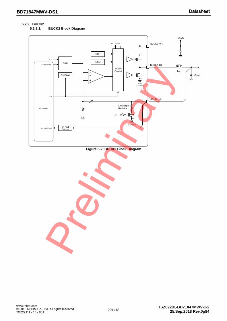
77/118 25.Sep.2018 Rev.0p84 © 2018 ROHM Co., Ltd. All rights reserved. www.rohm.com
TSZ22111 • 15 • 001
TSZ02201-BD71847MWV-1-2
BD71847MWV-DS1
5.2.2. BUCK2
5.2.2.1. BUCK2 Block Diagram
Figure 5-2. BUCK2 Block Diagram
Switch
Control LBK2
VSYS
OSC
COBK2
BUCK2_FB
Discharge
Resistor
BUCK2_VIN
BUCK2_LX
PGND
(EX P-PAD)
-Soft Start
+
-
DAC
INT LDO1P5
VR FaultDetector
GND
OCP
VR Fault S ignal
Voltage set ting
EN
EN
VREF
VR Controller
P GND
(EXP-PAD)
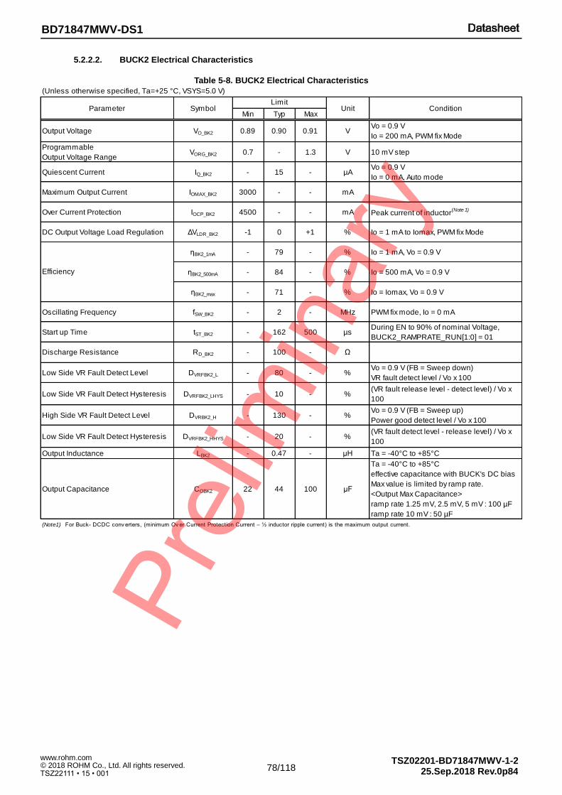
78/118 25.Sep.2018 Rev.0p84 © 2018 ROHM Co., Ltd. All rights reserved. www.rohm.com
TSZ22111 • 15 • 001
TSZ02201-BD71847MWV-1-2
BD71847MWV-DS1
5.2.2.2. BUCK2 Electrical Characteristics
Table 5-8. BUCK2 Electrical Characteristics
Min Typ Max
Output Voltage VO_BK2 0.89 0.90 0.91 VVo = 0.9 V
Io = 200 mA, PWM fix Mode
Programmable
Output Voltage RangeVORG_BK2 0.7 - 1.3 V 10 mV step
Quiescent Current IQ_BK2 - 15 - µAVo = 0.9 V
Io = 0 mA, Auto mode
Maximum Output Current IOMAX_BK2 3000 - - mA
Over Current Protection IOCP_BK2 4500 - - mA Peak current of inductor(Note 1)
DC Output Voltage Load Regulation ΔVLDR_BK2 -1 0 +1 % Io = 1 mA to Iomax, PWM fix Mode
ηBK2_1mA - 79 - % Io = 1 mA, Vo = 0.9 V
ηBK2_500mA - 84 - % Io = 500 mA, Vo = 0.9 V
ηBK2_max - 71 - % Io = Iomax, Vo = 0.9 V
Oscillating Frequency fSW_BK2 - 2 - MHz PWM fix mode, Io = 0 mA
Start up Time tST_BK2 - 162 500 µsDuring EN to 90% of nominal Voltage,
BUCK2_RAMPRATE_RUN[1:0] = 01
Discharge Resistance RD_BK2 - 100 - Ω
Low Side VR Fault Detect Level DVRFBK2_L - 80 - %Vo = 0.9 V (FB = Sweep down)
VR fault detect level / Vo x 100
Low Side VR Fault Detect Hysteresis DVRFBK2_LHYS - 10 - %(VR fault release level - detect level) / Vo x
100
High Side VR Fault Detect Level DVRBK2_H - 130 - %Vo = 0.9 V (FB = Sweep up)
Power good detect level / Vo x 100
Low Side VR Fault Detect Hysteresis DVRFBK2_HHYS - 20 - %(VR fault detect level - release level) / Vo x
100
Output Inductance LBK2 - 0.47 - μH Ta = -40°C to +85°C
Output Capacitance COBK2 22 44 100 μF
Ta = -40°C to +85°C
effective capacitance with BUCK's DC bias
Max value is limited by ramp rate.
<Output Max Capacitance>
ramp rate 1.25 mV, 2.5 mV, 5 mV : 100 µF
ramp rate 10 mV : 50 µF
Efficiency
(Note1) For Buck- DCDC conv erters, (minimum Ov er Current Protection Current – ½ inductor ripple current) is the maximum output current.
(Unless otherwise specified, Ta=+25 °C, VSYS=5.0 V)
Parameter SymbolLimit
Unit Condition

79/118 25.Sep.2018 Rev.0p84 © 2018 ROHM Co., Ltd. All rights reserved. www.rohm.com
TSZ22111 • 15 • 001
TSZ02201-BD71847MWV-1-2
BD71847MWV-DS1
5.2.2.3. BUCK2 Control
Table 5-9. BUCK2_CTRL - BUCK2 Control Register
Table 5-10. BUCK2_VOLT_RUN - BUCK2 Voltage (RUN) Register
Register Name R/W D7 D6 D5 D4 D3 D2 D1 D0 Initial Address
BUCK2_CTRL R/W - -BUCK2_
PWM_FIX- BUCK2_SEL BUCK2_EN 0x40 0x06
Bit
D[7:6]
D[3]
D[1]
D[0]
BUCK2_RAMPRATE[1:0]
BUCK2 DVS ramp rate
00 = 10 mV/μs
01 = 5 mV/μs
10 = 2.5 mV/μs
11 = 1.25 mV/μs
Note : When BUCK2 voltage starts up from 0V,
the ramp rate is fixed 5mV/μs, regardless of the value of
BUCK2_RAMPRATE[1:0].
01
BUCK2_RAMPRATE[1:0]
Name Function Initial
0
BUCK2_EN
BUCK2 control bit with condition of D[1]
0 = BUCK2 OFF
1 = BUCK2 ON
This bit returns to 0 at the beginning of PWROFF sequence or emergency
shutdown.
When system is in SNVS or SUSPEND, BUCK2_SEL = 1 and BUCK2_EN = 1,
BUCK2 voltage is specified by BUCK2_VOLT_IDLE register.
0
BUCK2_PWM_FIX
0 – AUTO PWM/PFM mode
VR adjusts the operating mode (PFM/PWM) automatically based on the load
current to maximize power efficiency.
1 – Forced PWM Mode
VR operates in PWM mode only.
0
BUCK2_SEL
BUCK2 control select bit
0 = BUCK2 ON/OFF is controlled by state machine.
1 = BUCK2 ON/OFF is controlled by D[0] on this register.
Register Name R/W D7 D6 D5 D4 D3 D2 D1 D0 Initial Address
BUCK2_VOLT_RUN R/W - 0x14 0x10
Bit
D[5:0]
BUCK2_VOLT_RUN[6:0]
BUCK2_VOLT_RUN[6:0]
BUCK2 voltage when Power State = RUN
0x00 = 0.70V 0x01 = 0.71V 0x02 = 0.72V 0x03 = 0.73V
0x04 = 0.74V 0x05 = 0.75V 0x06 = 0.76V 0x07 = 0.77V
0x08 = 0.78V 0x09 = 0.79V 0x0A = 0.80V 0x0B = 0.81V
0x0C = 0.82V 0x0D = 0.83V 0x0E = 0.84V 0x0F = 0.85V
0x10 = 0.86V 0x11 = 0.87V 0x12 = 0.88V 0x13 = 0.89V
0x14 = 0.90V (initial)
0x15 = 0.91V 0x16 = 0.92V 0x17 = 0.93V 0x18 = 0.94V
0x19 = 0.95V 0x1A = 0.96V 0x1B = 0.97V 0x1C = 0.98V
0x1D = 0.99V 0x1E = 1.00V 0x1F = 1.01V 0x20 = 1.02V
0x21 = 1.03V 0x22 = 1.04V 0x23 = 1.05V 0x24 = 1.06V
0x25 = 1.07V 0x26 = 1.08V 0x27 = 1.09V 0x28 = 1.10V
0x29 = 1.11V 0x2A = 1.12V 0x2B = 1.13V 0x2C = 1.14V
0x2D = 1.15V 0x2E = 1.16V 0x2F = 1.17V 0x30 = 1.18V
0x31 = 1.19V 0x32 = 1.20V 0x33 = 1.21V 0x34 = 1.22V
0x35 = 1.23V 0x36 = 1.24V 0x37 = 1.25V 0x38 = 1.26V
0x39 = 1.27V 0x3A = 1.28V 0x3B = 1.29V 0x3C = 1.30V
0x3D-0x7F = reserved
0010100
Name Function Initial
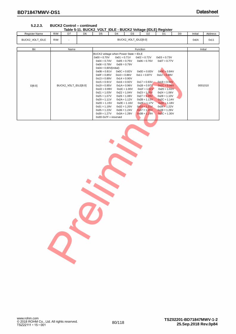
80/118 25.Sep.2018 Rev.0p84 © 2018 ROHM Co., Ltd. All rights reserved. www.rohm.com
TSZ22111 • 15 • 001
TSZ02201-BD71847MWV-1-2
BD71847MWV-DS1
5.2.2.3. BUCK2 Control – continued Table 5-11. BUCK2_VOLT_IDLE - BUCK2 Voltage (IDLE) Register
Register Name R/W D7 D6 D5 D4 D3 D2 D1 D0 Initial Address
BUCK2_VOLT_IDLE R/W - 0x0A 0x11
Bit
D[6:0]
BUCK2_VOLT_IDLE[6:0]
Name Function Initial
BUCK2_VOLT_IDLE[6:0]
BUCK2 voltage when Power State = IDLE
0x00 = 0.70V 0x01 = 0.71V 0x02 = 0.72V 0x03 = 0.73V
0x04 = 0.74V 0x05 = 0.75V 0x06 = 0.76V 0x07 = 0.77V
0x08 = 0.78V 0x09 = 0.79V
0x0A = 0.80V(initial)
0x0B = 0.81V 0x0C = 0.82V 0x0D = 0.83V 0x0E = 0.84V
0x0F = 0.85V 0x10 = 0.86V 0x11 = 0.87V 0x12 = 0.88V
0x13 = 0.89V 0x14 = 0.90V
0x15 = 0.91V 0x16 = 0.92V 0x17 = 0.93V 0x18 = 0.94V
0x19 = 0.95V 0x1A = 0.96V 0x1B = 0.97V 0x1C = 0.98V
0x1D = 0.99V 0x1E = 1.00V 0x1F = 1.01V 0x20 = 1.02V
0x21 = 1.03V 0x22 = 1.04V 0x23 = 1.05V 0x24 = 1.06V
0x25 = 1.07V 0x26 = 1.08V 0x27 = 1.09V 0x28 = 1.10V
0x29 = 1.11V 0x2A = 1.12V 0x2B = 1.13V 0x2C = 1.14V
0x2D = 1.15V 0x2E = 1.16V 0x2F = 1.17V 0x30 = 1.18V
0x31 = 1.19V 0x32 = 1.20V 0x33 = 1.21V 0x34 = 1.22V
0x35 = 1.23V 0x36 = 1.24V 0x37 = 1.25V 0x38 = 1.26V
0x39 = 1.27V 0x3A = 1.28V 0x3B = 1.29V 0x3C = 1.30V
0x3D-0x7F = reserved
0001010

81/118 25.Sep.2018 Rev.0p84 © 2018 ROHM Co., Ltd. All rights reserved. www.rohm.com
TSZ22111 • 15 • 001
TSZ02201-BD71847MWV-1-2
BD71847MWV-DS1
5.2.3. BUCK5
5.2.3.1. BUCK5 Block Diagram
Figure 5-3. BUCK5 Block Diagram
Switch
Control LBK5
VSYS
OSC
COBK5
BUCK5_FB
Discharge
Resistor
BUCK5_VIN
BUCK5_LX
PGND
(EX P-PAD)
-Soft Start
+
-
DAC
INT LDO1P5
VR FaultDetector
GND
OCP
VR Fault S ignal
Voltage set ting
EN
EN
VREF
VR Controller
PGND
(EX P-PAD)

82/118 25.Sep.2018 Rev.0p84 © 2018 ROHM Co., Ltd. All rights reserved. www.rohm.com
TSZ22111 • 15 • 001
TSZ02201-BD71847MWV-1-2
BD71847MWV-DS1
5.2.3.2. BUCK5 Electrical Characteristics
Table 5-12. BUCK5 Electrical Characteristics
Min Typ Max
Output Voltage VO_BK5 0.89 0.90 0.91 VVo = 0.9 V
Io = 200 mA, PWM fix Mode
Programmable
Output Voltage RangeVORG_BK5 0.70 - 1.35 V
0.70 V, 0.80 V, 0.90 V, 1.00 V,
1.05 V, 1.10 V, 1.20 V, 1.35 V
Quiescent Current IQ_BK5 - 15 - µAVo = 0.9 V
Io = 0 mA, Auto mode
Maximum Output Current IOMAX_BK5 3000 - - mA
Over Current Protection IOCP_BK5 4500 - - mA Peak current of inductor(Note 1)
DC Output Voltage Load Regulation ΔVLDR_BK5 -1 0 +1 % Io = 1 mA to Iomax, PWM fix Mode
ηBK5_1mA - 79 - % Io = 1 mA, Vo = 0.9 V
ηBK5_500mA - 84 - % Io = 500 mA, Vo = 0.9 V
ηBK5_max - 71 - % Io = Iomax, Vo = 0.9 V
Oscillating Frequency fSW_BK5 - 2 - MHz PWM fix mode, Io = 0 mA
Start up Time tST_BK5 - 162 500 µs During EN to 90% of nominal Voltage
Discharge Resistance RD_BK5 - 100 - Ω
Low Side VR Fault Detect Level DVRFBK5_L - 80 - %Vo = 0.9 V (FB = Sweep down)
VR fault detect level / Vo x 100
Low Side VR Fault Detect Hysteresis DVRFBK5_LHYS - 10 - %(VR fault release level - detect level) / Vo x
100
High Side VR Fault Detect Level DVRBK5_H - 130 - %Vo = 0.9 V (FB = Sweep up)
Power good detect level / Vo x 100
Low Side VR Fault Detect Hysteresis DVRFBK5_HHYS - 20 - %(VR fault detect level - release level) / Vo x
100
Output Inductance LBK5 - 0.47 - μH Ta = -40°C to +85°C
Output Capacitance COBK5 22 44 100 μFTa = -40°C to +85°C
effective capacitance with BUCK's DC bias
Efficiency
(Note1) For Buck- DCDC conv erters, (minimum Ov er Current Protection Current – ½ inductor ripple current) is the maximum output current.
(Unless otherwise specified, Ta=+25 °C, VSYS=5.0 V)
Parameter SymbolLimit
Unit Condition

83/118 25.Sep.2018 Rev.0p84 © 2018 ROHM Co., Ltd. All rights reserved. www.rohm.com
TSZ22111 • 15 • 001
TSZ02201-BD71847MWV-1-2
BD71847MWV-DS1
5.2.3.3. BUCK5 Control
Table 5-13. BUCK5_CTRL - BUCK5 Control Register
Table 5-14. BUCK5_VOLT - BUCK5 Voltage Register
Register Name R/W D7 D6 D5 D4 D3 D2 D1 D0 Initial Address
BUCK5_CTRL R/W - - - -BUCK5_PW
M_FIX- BUCK5_SEL BUCK5_EN 0x00 0x09
Bit
D[3]
D[1]
D[0]
BUCK5_PWM_FIX
0 – AUTO PWM/PFM mode
VR adjusts the operating mode (PFM/PWM) automatically based on the load
current to maximize power efficiency.
1 – Forced PWM Mode
VR operates in PWM mode only.
0
Name Function Initial
BUCK5_SEL
BUCK5 control select bit
0 = BUCK5 ON/OFF is controlled by state machine.
1 = BUCK5 ON/OFF is controlled by D[0] on this register.
0
BUCK5_EN
BUCK5 control bit with condition of D[1]
0 = BUCK5 OFF
1 = BUCK5 ON
This bit returns to 0 at the beginning of PWROFF sequence or emergency
shutdown.
0
Register Name R/W D7 D6 D5 D4 D3 D2 D1 D0 Initial Address
BUCK5_VOLT R/W - - - 0x02 0x14
Bit
D[7:6]
D[2:0]
BUCK5_VOLT[2:0]
BUCK5_VOLT[2:0]
BUCK5 voltage
If D[7:6]=00
000 = 0.70 V 001 = 0.80 V 010 = 0.90 V (Initial) 011 = 1.00 V
100 = 1.05 V 101 = 1.10 V 110 = 1.20 V 111 = 1.35 V
If D[7:6]=01
000 = 0.55 V 001 = 0.60 V 010 = 0.65 V 011 = 0.70 V
100 = 0.75 V 101 = 0.80 V 110 = 0.85 V 111 = 0.90 V
If D[7:6]=10
000 = 0.675 V 001 = 0.775 V 010 = 0.875 V 011 = 0.975 V
100 = 1.025 V 101 = 1.075 V 110 = 1.175 V 111 = 1.325 V
Note: Changing BUCK5 voltage value is not allowed when BUCK5 is still ON.
In the case where this register value is changed, BUCK5 should be turned
OFF.
010
Name Function Initial
BUCK5_VOLT_SEL[1:0]
Select the BUCK5 voltage range set by D[2:0].
00 = 0.70 V to 1.35 V 01 = 0.55 V to 0.90 V
10 = 0.675 V to 1.325 V 11 = reserved
Note: Changing BUCK5 voltage value is not allowed when BUCK5 is still ON.
In the case where this register value is changed, BUCK5 should be turned
OFF.
00
BUCK5_
VOLT_SEL[1:0]

84/118 25.Sep.2018 Rev.0p84 © 2018 ROHM Co., Ltd. All rights reserved. www.rohm.com
TSZ22111 • 15 • 001
TSZ02201-BD71847MWV-1-2
BD71847MWV-DS1
5.2.4. BUCK6
5.2.4.1. BUCK6 Block Diagram
Figure 5-4. BUCK6 Block Diagram
Switch
Control LBK6
VSYS
OSC
COBK6
BUCK6_FB
Discharge
Resistor
BUCK6_VIN
BUCK6_LX
PGND
(EX P-PAD)
-Soft Start
+
-
DAC
INT LDO1P5
VR FaultDetector
GND
OCP
VR Fault S ignal
Voltage set ting
EN
EN
VREF
VR Controller
PGND
(EXP-PAD)

85/118 25.Sep.2018 Rev.0p84 © 2018 ROHM Co., Ltd. All rights reserved. www.rohm.com
TSZ22111 • 15 • 001
TSZ02201-BD71847MWV-1-2
BD71847MWV-DS1
5.2.4.2. BUCK6 Electrical Characteristics
Table 5-15. BUCK6 Electrical Characteristics
Headroom for BUCK6
BUCK6 can’t maintain output voltage when the input voltage close to output voltage. The headroom voltage is determined by output current and the impedance from VSYS to BUCK6 output including the inductor parasitic impedance (DCR). The PMIC internal impedance from BUCK6_VIN to BUCK6_LX is 121 mΩ at the worst case. Please calculate total impedance using this value, and secure enough headroom for VSYS according to the output current and voltage. (Example – ROHM EVB case) Vo = 3.3V setting: VO
VSYS to BUCK6_VIN impedance of the EVB = 3 mΩ: RVIN BUCK6_LX to inductor impedance of the EVB = 6 mΩ: RLX Inductor parasitic impedance (DCR) = 45 mΩ: RIND PMIC internal impedance from BUCK6_VIN to BUC6_LX = 121 mΩ: RPMIC Total impedance = 175 mΩ: RTOTAL=RVIN+RLX+RIND+RPMIC Headroom = RTOTAL x Output Current
Output current Required minimum VSYS voltage
1.0 A 3.475 V
2.0 A 3.650 V
3.0 A 3.825 V
Min Typ Max
Output Voltage VO_BK6 3.267 3.300 3.333 VVo=3.3 V
Io = 200 mA, PWM fix Mode
Programmable
Output Voltage RangeVORG_BK6 2.6 - 3.3 V 100 mV step
Quiescent Current IQ_BK6 - 9 - µAVo=3.3 V
Io=0 mA, Auto mode
Maximum Output Current IOMAX_BK6 3000 - - mA
Over Current Protection IOCP_BK6 4500 - - mA Peak current of inductor(Note 1)
DC Output Voltage Load Regulation ΔVLDR_BK6 -1 0 +1 % Io=1 mA to Iomax, PWM fix Mode
ηBK6_1mA - 93 - % Io = 1 mA, Vo=3.3 V
ηBK6_500mA - 95 - % Io = 500 mA, Vo=3.3 V
ηBK6_max - 88 - % Io = Iomax, Vo=3.3 V
Oscillating Frequency fSW_BK6 - 1.5 - MHz PWM fix mode, Io = 0 mA
Start up Time tST_BK6 - 240 500 µs During EN to 90% of nominal Voltage
Discharge Resistance RD_BK6 - 100 - Ω
Low Side VR Fault Detect Level DVRFBK6_L - 80 - %Vo = 3.3 V (FB = Sweep down)
VR fault detect level / Vo x 100
Low Side VR Fault Detect Hysteresis DVRFBK6_LHYS - 10 - %(VR fault release level - detect level) / Vo x
100
High Side VR Fault Detect Level DVRBK6_H - 130 - %Vo = 3.3 V (FB = Sweep up)
Power good detect level / Vo x 100
Low Side VR Fault Detect Hysteresis DVRFBK6_HHYS - 20 - %(VR fault detect level - release level) / Vo x
100
Output Inductance LBK6 - 1 - μH Ta = -40°C to +85°C
Output Capacitance COBK6 22 44 100 μFTa = -40°C to +85°C
effective capacitance with BUCK's DC bias
Efficiency
(Note1) For Buck- DCDC conv erters, (minimum Ov er Current Protection Current – ½ inductor ripple current) is the maximum output current.
(Unless otherwise specified, Ta=+25 °C, VSYS=5.0 V)
Parameter SymbolLimit
Unit Condition

86/118 25.Sep.2018 Rev.0p84 © 2018 ROHM Co., Ltd. All rights reserved. www.rohm.com
TSZ22111 • 15 • 001
TSZ02201-BD71847MWV-1-2
BD71847MWV-DS1
5.2.4.3. BUCK6 Control
Table 5-16. BUCK6_CTRL - BUCK6 Control Register
Table 5-17. BUCK6_VOLT - BUCK6 Voltage Register
Register Name R/W D7 D6 D5 D4 D3 D2 D1 D0 Initial Address
BUCK6_CTRL R/W - - - -BUCK6_PW
M_FIX- BUCK6_SEL BUCK6_EN 0x00 0x0A
Bit
D[3]
D[1]
D[0]
BUCK6_SEL
BUCK6 control select bit
0 = BUCK6 ON/OFF is controlled by state machine.
1 = BUCK6 ON/OFF is controlled by D[0] on this register.
0
BUCK6_EN
BUCK6 control bit with condition of D[1]
0 = BUCK6 OFF
1 = BUCK6 ON
This bit returns to 0 at the beginning of PWROFF sequence or emergency
shutdown.
0
Name Function Initial
BUCK6_PWM_FIX
0 – AUTO PWM/PFM mode
VR adjusts the operating mode (PFM/PWM) automatically based on the load
current to maximize power efficiency.
1 – Forced PWM Mode
VR operates in PWM mode only.
0
Register Name R/W D7 D6 D5 D4 D3 D2 D1 D0 Initial Address
BUCK6_VOLT R/W -BUCK6_
VOLT_SEL- - - - 0x03 0x15
Bit
D[6]
D[1:0]
BUCK6_VOLT[1:0]
BUCK6_VOLT[1:0]
BUCK6 voltage
If D[6]=0
00 = 3.0 V 01 = 3.1 V 10 = 3.2 V 11 = 3.3 V(Initial)
If D[6]=1
00 = 2.6 V 01 = 2.7 V 10 = 2.8 V 11 = 2.9 V
Note: Changing BUCK6 voltage value is not allowed when BUCK6 is still ON.
In the case where this register value is changed, BUCK6 should be turned
OFF.
11
Name Function Initial
BUCK6_VOLT_SEL
Select the BUCK6 voltage range set by D[6].
0 =3.0 V to 3.3 V 1 = 2.6 V to 2.9 V
Note: Changing BUCK6 voltage value is not allowed when BUCK6 is still ON.
In the case where this register value is changed, BUCK6 should be turned
OFF.
0

87/118 25.Sep.2018 Rev.0p84 © 2018 ROHM Co., Ltd. All rights reserved. www.rohm.com
TSZ22111 • 15 • 001
TSZ02201-BD71847MWV-1-2
BD71847MWV-DS1
5.2.5. BUCK7
5.2.5.1. BUCK7 Block Diagram
Figure 5-5. BUCK7 Block Diagram
Switch
Control LBK7
VSYS
OSC
COBK7
BUCK7_FB
Discharge
Resistor
BUCK7_VIN
BUCK7_LX
PGND
(EX P-PAD)
-Soft Start
+
-
DAC
INT LDO1P5
VR FaultDetector
GND
OCP
VR Fault S ignal
Voltage set ting
EN
EN
VREF
VR Controller
PGND
(EXP-PAD)

88/118 25.Sep.2018 Rev.0p84 © 2018 ROHM Co., Ltd. All rights reserved. www.rohm.com
TSZ22111 • 15 • 001
TSZ02201-BD71847MWV-1-2
BD71847MWV-DS1
5.2.5.2. BUCK7 Electrical Characteristics
Table 5-18. BUCK7 Electrical Characteristics
Min Typ Max
Output Voltage VO_BK7 1.782 1.800 1.818 VVo = 1.8 V
Io = 200 mA, PWM fix Mode
Programmable
Output Voltage RangeVORG_BK7 1.605 - 1.995 V
1.605 V, 1.695 V, 1.755 V, 1.800 V,
1.845 V, 1.905 V, 1.950 V, 1.995 V
Quiescent Current IQ_BK7 - 15 - µAVo = 1.8 V
Io = 0 mA, Auto mode
Maximum Output Current IOMAX_BK7 1500 - - mA
Over Current Protection IOCP_BK7 3000 - - mA Peak current of inductor(Note 1)
DC Output Voltage Load Regulation ΔVLDR_BK7 -1 0 +1 % Io = 1 mA to Iomax, PWM fix Mode
ηBK7_1mA - 85 - % Io = 1 mA, Vo=1.8 V
ηBK7_500mA - 89 - % Io = 500 mA, Vo=1.8 V
ηBK7_max - 85 - % Io = Iomax, Vo=1.8 V
Oscillating Frequency fSW_BK7 - 2 - MHz PWM fix mode, Io = 0 mA
Start up Time tST_BK7 - 220 500 µs During EN to 90% of nominal Voltage
Discharge Resistance RD_BK7 - 100 - Ω
Low Side VR Fault Detect Level DVRFBK7_L - 80 - %Vo = 1.8 V (FB = Sweep down)
VR fault detect level / Vo x 100
Low Side VR Fault Detect Hysteresis DVRFBK7_LHYS - 10 - %(VR fault release level - detect level) / Vo x
100
High Side VR Fault Detect Level DVRBK7_H - 130 - %Vo = 1.8 V (FB = Sweep up)
Power good detect level / Vo x 100
Low Side VR Fault Detect Hysteresis DVRFBK7_HHYS - 20 - %(VR fault detect level - release level) / Vo x
100
Output Inductance LBK7 - 0.47 - μH Ta = -40°C to +85°C
Output Capacitance COBK7 11 22 100 μFTa = -40°C to +85°C
effective capacitance with BUCK's DC bias
Efficiency
(Note1) For Buck- DCDC conv erters, (minimum Ov er Current Protection Current – ½ inductor ripple current) is the maximum output current.
(Unless otherwise specified, Ta=+25 °C, VSYS=5.0 V)
Parameter SymbolLimit
Unit Condition
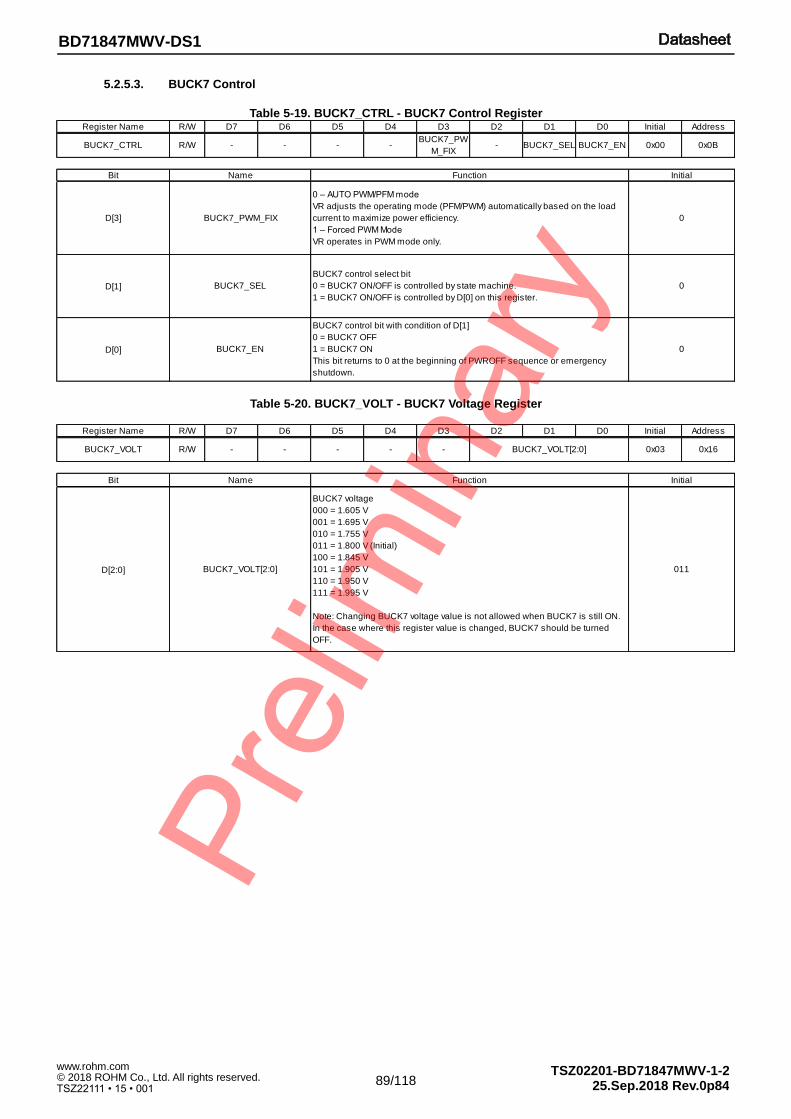
89/118 25.Sep.2018 Rev.0p84 © 2018 ROHM Co., Ltd. All rights reserved. www.rohm.com
TSZ22111 • 15 • 001
TSZ02201-BD71847MWV-1-2
BD71847MWV-DS1
5.2.5.3. BUCK7 Control
Table 5-19. BUCK7_CTRL - BUCK7 Control Register
Table 5-20. BUCK7_VOLT - BUCK7 Voltage Register
Register Name R/W D7 D6 D5 D4 D3 D2 D1 D0 Initial Address
BUCK7_CTRL R/W - - - -BUCK7_PW
M_FIX- BUCK7_SEL BUCK7_EN 0x00 0x0B
Bit
D[3]
D[1]
D[0]
BUCK7_SEL
BUCK7 control select bit
0 = BUCK7 ON/OFF is controlled by state machine.
1 = BUCK7 ON/OFF is controlled by D[0] on this register.
0
BUCK7_EN
BUCK7 control bit with condition of D[1]
0 = BUCK7 OFF
1 = BUCK7 ON
This bit returns to 0 at the beginning of PWROFF sequence or emergency
shutdown.
0
Name Function Initial
BUCK7_PWM_FIX
0 – AUTO PWM/PFM mode
VR adjusts the operating mode (PFM/PWM) automatically based on the load
current to maximize power efficiency.
1 – Forced PWM Mode
VR operates in PWM mode only.
0
Register Name R/W D7 D6 D5 D4 D3 D2 D1 D0 Initial Address
BUCK7_VOLT R/W - - - - - 0x03 0x16
Bit
D[2:0]
BUCK7_VOLT[2:0]
BUCK7_VOLT[2:0]
BUCK7 voltage
000 = 1.605 V
001 = 1.695 V
010 = 1.755 V
011 = 1.800 V (Initial)
100 = 1.845 V
101 = 1.905 V
110 = 1.950 V
111 = 1.995 V
Note: Changing BUCK7 voltage value is not allowed when BUCK7 is still ON.
In the case where this register value is changed, BUCK7 should be turned
OFF.
011
Name Function Initial

90/118 25.Sep.2018 Rev.0p84 © 2018 ROHM Co., Ltd. All rights reserved. www.rohm.com
TSZ22111 • 15 • 001
TSZ02201-BD71847MWV-1-2
BD71847MWV-DS1
5.2.6. BUCK8
5.2.6.1. BUCK8 Block Diagram
Figure 5-6. BUCK8 Block Diagram
Switch
Control LBK8
VSYS
OSC
COBK8
BUCK8_FB
Discharge
Resistor
BUCK8_VIN
BUCK8_LX
PGND
(EXP-PAD)
-Soft Start
+
-
DAC
INT LDO 1P5
VR FaultDetector
GND
OCP
VR Fault S ignal
Voltage set ting
EN
PGND
(EXP-PAD)
EN
VRE F
VR Controller

91/118 25.Sep.2018 Rev.0p84 © 2018 ROHM Co., Ltd. All rights reserved. www.rohm.com
TSZ22111 • 15 • 001
TSZ02201-BD71847MWV-1-2
BD71847MWV-DS1
5.2.6.2. BUCK8 Electrical Characteristics
Table 5-21. BUCK8 Electrical Characteristics
Min Typ Max
Output Voltage VO_BK8 1.089 1.100 1.111 VVo = 1.1 V
Io = 200 mA, PWM fix Mode
Programmable
Output Voltage RangeVORG_BK8 0.8 - 1.4 V 10 mV step
Quiescent Current IQ_BK8 - 15 - µAVo = 1.1 V
Io = 0 mA, Auto mode
Maximum Output Current IOMAX_BK8 3000 - - mA
Over Current Protection IOCP_BK8 4500 - - mA Peak current of inductor (note 1)
DC Output Voltage Load Regulation ΔVLDR_BK8 -1 0 +1 % Io = 1 mA to Iomax, PWM fix Mode
ηBK8_1mA - 82 - % Io = 1 mA, Vo=1.1 V
ηBK8_500mA - 86 - % Io = 500 mA, Vo=1.1 V
ηBK8_max - 75 - % Io = Iomax, Vo=1.1 V
Oscillating Frequency fSW_BK8 - 2 - MHz PWM fix mode, Io = 0 mA
Start up Time tST_BK8 - 200 500 µs During EN to 90% of nominal Voltage
Discharge Resistance RD_BK8 - 100 - Ω
Low Side VR Fault Detect Level DVRFBK7_L - 80 - %Vo = 1.1 V (FB = Sweep down)
VR fault detect level / Vo x 100
Low Side VR Fault Detect Hysteresis DVRFBK7_LHYS - 10 - %(VR fault release level - detect level) / Vo x
100
High Side VR Fault Detect Level DVRBK7_H - 130 - %Vo = 1.1 V (FB = Sweep up)
Power good detect level / Vo x 100
Low Side VR Fault Detect Hysteresis DVRFBK7_HHYS - 20 - %(VR fault detect level - release level) / Vo x
100
Output Inductance LBK8 - 0.47 - μH Ta = -40°C to +85°C
Output Capacitance COBK8 22 44 100 μFTa = -40°C to +85°C
effective capacitance with BUCK's DC bias
Efficiency
(Note1) For Buck- DCDC conv erters, (minimum Ov er Current Protection Current – ½ inductor ripple current) is the maximum output current.
(Unless otherwise specified, Ta=+25 °C, VSYS=5.0 V)
Parameter SymbolLimit
Unit Condition

92/118 25.Sep.2018 Rev.0p84 © 2018 ROHM Co., Ltd. All rights reserved. www.rohm.com
TSZ22111 • 15 • 001
TSZ02201-BD71847MWV-1-2
BD71847MWV-DS1
5.2.6.3. BUCK8 Control
Table 5-22. BUCK8_CTRL - BUCK8 Control Register
Table 5-23. BUCK8_VOLT - BUCK8 Voltage Register
Register Name R/W D7 D6 D5 D4 D3 D2 D1 D0 Initial Address
BUCK8_CTRL R/W - - - -BUCK8_PW
M_FIX- BUCK8_SEL BUCK8_EN 0x00 0x0C
Bit
D[3]
D[1]
D[0]
BUCK8_SEL
BUCK8 control select bit
0 = BUCK8 ON/OFF is controlled by state machine.
1 = BUCK8 ON/OFF is controlled by D[0] on this register.
0
BUCK8_EN
BUCK8 control bit with condition of D[1]
0 = BUCK8 OFF
1 = BUCK8 ON
This bit returns to 0 at the beginning of PWROFF sequence or emergency
shutdown.
0
Name Function Initial
BUCK8_PWM_FIX
0 – AUTO PWM/PFM mode
VR adjusts the operating mode (PFM/PWM) automatically based on the load
current to maximize power efficiency.
1 – Forced PWM Mode
VR operates in PWM mode only.
0
Register Name R/W D7 D6 D5 D4 D3 D2 D1 D0 Initial Address
BUCK8_VOLT R/W - 0x1E 0x17
Bit
D[6:0]
BUCK8_VOLT[6:0]
BUCK8_VOLT[6:0]
BUCK8 voltage
0x00 = 0.80 V 0x01 = 0.81 V 0x02 = 0.82 V 0x03 = 0.83 V
0x04 = 0.84 V 0x05 = 0.85 V 0x06 = 0.86 V 0x07 = 0.87 V
0x08 = 0.88 V 0x09 = 0.89 V 0x0A = 0.90 V 0x0B = 0.91 V
0x0C = 0.92 V 0x0D = 0.93 V 0x0E = 0.94 V 0x0F = 0.95 V
0x10 = 0.96 V 0x11 = 0.97 V 0x12 = 0.98 V 0x13 = 0.99 V
0x14 = 1.00 V 0x15 = 1.01 V 0x16 = 1.02 V 0x17 = 1.03 V
0x18 = 1.04 V 0x19 = 1.05 V 0x1A = 1.06 V 0x1B = 1.07 V
0x1C = 1.08 V 0x1D = 1.09 V
0x1E = 1.10 V (initial)
0x1F = 1.11 V 0x20 = 1.12 V 0x21 = 1.13 V 0x22 = 1.14 V
0x23 = 1.15 V 0x24 = 1.16 V 0x25 = 1.17 V 0x26 = 1.18 V
0x27 = 1.19 V 0x28 = 1.20 V 0x29 = 1.21 V 0x2A = 1.22 V
0x2B = 1.23 V 0x2C = 1.24 V 0x2D = 1.25 V 0x2E = 1.26 V
0x2F = 1.27 V 0x30 = 1.28 V 0x31 = 1.29 V 0x32 = 1.30 V
0x33 = 1.31 V 0x34 = 1.32 V 0x35 = 1.33 V 0x36 = 1.34 V
0x37 = 1.35 V 0x38 = 1.36 V 0x39 = 1.37 V 0x3A = 1.38 V
0x3B = 1.39 V 0x3C = 1.40 V
0x3D-0x7F = reserved
Note: Changing BUCK8 voltage value is not allowed when BUCK8 is still ON.
In the case where this register value is changed, BUCK8 should be turned
OFF.
0011110
Name Function Initial

93/118 25.Sep.2018 Rev.0p84 © 2018 ROHM Co., Ltd. All rights reserved. www.rohm.com
TSZ22111 • 15 • 001
TSZ02201-BD71847MWV-1-2
BD71847MWV-DS1
5.3. Details of LDO
5.3.1. LDO1
5.3.1.1. LDO1 Block Diagram
Figure 5-7. LDO1 Block Diagram
VSYS
VSYS
COLDO1
Discharge
Resistor
-Soft Start
+
-
DAC
VR FaultDetector
GND
OCP
VR Fault S ignal
Voltage set ting
EN
PGND
(EXP-PAD)
EN
LDO1_VOUT
VREF
VR Controller

94/118 25.Sep.2018 Rev.0p84 © 2018 ROHM Co., Ltd. All rights reserved. www.rohm.com
TSZ22111 • 15 • 001
TSZ02201-BD71847MWV-1-2
BD71847MWV-DS1
5.3.1.2. LDO1 Electrical Characteristics
Table 5-24. LDO1 Electrical Characteristics
Min Typ Max
Output Voltage VO_LDO1 1.782 1.800 1.818 VVO=1.8 V setting
Io=1 mA
Output Voltage Range 1 VORG_LDO1_1 1.600 - 1.900 V 100 mV step
Output Voltage Range 2 VORG_LDO1_2 3.000 - 3.300 V 100 mV step
Maximum Output Current IOMAX_LDO1 10 - - mA
Over Current Protection IOCP_LDO1 20 - - mA
Quiescent Current IQ_LDO1 - 6 - µA Io=0 mA
Dropout Voltage ΔVODP_LDO1 - 40 - mVIo = Iomax
VSYS=3.2 V, VO=3.3 V setting
Start up Time tST_LDO1 - 440 1000 µsIo=0 mA,
During EN to 90% of nominal Voltage
DC Output Voltage Load Regulation ΔVLDR_LDO1 - 10 20 mV Io=1 mA to Iomax
DC Output Voltage Line Regulation ΔVLNR_LDO1 - 2 5 mV VSYS = 4.5 V to 5.5 V, Io=Iomax
Discharge Resistance RDIS_LDO1 - 100 200 Ω
VR Fault Detect Level DVRFLDO1 - 80 - %Output = Sweep down
Power good detect level / Vo x 100
VR Fault Detect Hysteresis DVRFLDO1_HYS - 10 - %(VR fault release level - detect level) / Vo x
100
Ripple Rejection Ratio RRLDO1 - 60 - dB
VSYS = 5.0 V, IO=Iomax/2
VR = -20 dBV, fR=100 Hz
BW=20 Hz to 20 kHz
Output Capacitance COLDO1 0.5 1.0 5.0 μFTa = -40°C to +85°C,
effective capacitance with LDO's DC bias
(Unless otherwise specified, Ta = +25°C, VSYS = 5.0 V, VIN_3P3 = 3.3 V, VIN_1P8_1 = 1.8 V, Vo = 1.8 V setting)
Parameter SymbolLimit
Unit Condition
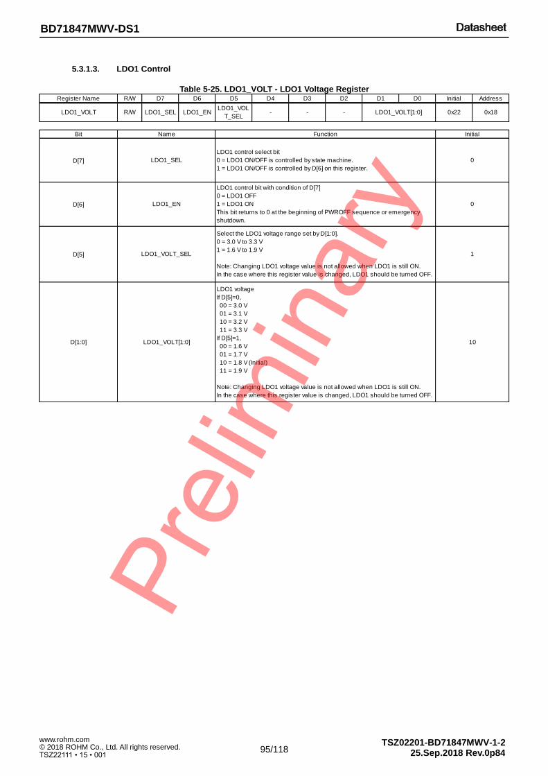
95/118 25.Sep.2018 Rev.0p84 © 2018 ROHM Co., Ltd. All rights reserved. www.rohm.com
TSZ22111 • 15 • 001
TSZ02201-BD71847MWV-1-2
BD71847MWV-DS1
5.3.1.3. LDO1 Control
Table 5-25. LDO1_VOLT - LDO1 Voltage Register
Register Name R/W D7 D6 D5 D4 D3 D2 D1 D0 Initial Address
LDO1_VOLT R/W LDO1_SEL LDO1_ENLDO1_VOL
T_SEL- - - 0x22 0x18
Bit
D[7]
D[6]
D[5]
D[1:0] LDO1_VOLT[1:0]
LDO1 voltage
If D[5]=0,
00 = 3.0 V
01 = 3.1 V
10 = 3.2 V
11 = 3.3 V
If D[5]=1,
00 = 1.6 V
01 = 1.7 V
10 = 1.8 V (Initial)
11 = 1.9 V
Note: Changing LDO1 voltage value is not allowed when LDO1 is still ON.
In the case where this register value is changed, LDO1 should be turned OFF.
10
LDO1_VOLT[1:0]
Name Function Initial
LDO1_SEL
LDO1_EN
LDO1 control select bit
0 = LDO1 ON/OFF is controlled by state machine.
1 = LDO1 ON/OFF is controlled by D[6] on this register.
LDO1 control bit with condition of D[7]
0 = LDO1 OFF
1 = LDO1 ON
This bit returns to 0 at the beginning of PWROFF sequence or emergency
shutdown.
0
0
LDO1_VOLT_SEL
Select the LDO1 voltage range set by D[1:0].
0 = 3.0 V to 3.3 V
1 = 1.6 V to 1.9 V
Note: Changing LDO1 voltage value is not allowed when LDO1 is still ON.
In the case where this register value is changed, LDO1 should be turned OFF.
1

96/118 25.Sep.2018 Rev.0p84 © 2018 ROHM Co., Ltd. All rights reserved. www.rohm.com
TSZ22111 • 15 • 001
TSZ02201-BD71847MWV-1-2
BD71847MWV-DS1
5.3.2. LDO2 5.3.2.1. LDO2 Block Diagram
Figure 5-8. LDO2 Block Diagram
VSYS
VSYS
COLDO2
Discharge
Resistor
-Soft Start
+
-
DAC
VR FaultDetector
GND
OCP
VR Fault S ignal
Voltage set ting
EN
PGND
(EXP-PAD)
EN
LDO2_VOUT
VREF
VR Controller

97/118 25.Sep.2018 Rev.0p84 © 2018 ROHM Co., Ltd. All rights reserved. www.rohm.com
TSZ22111 • 15 • 001
TSZ02201-BD71847MWV-1-2
BD71847MWV-DS1
5.3.2.2. LDO2 Electrical Characteristics
Table 5-26. LDO2 Electrical Characteristics
5.3.2.3. LDO2 Control
Table 5-27. LDO2_VOLT - LDO2 Voltage Register
Min Typ Max
Output Voltage VO_LDO2 0.785 0.800 0.815 VVO=0.8 V setting
Io=1 mA
Output Voltage Range VORG_LDO2 0.800 - 0.900 V 100 mV step
Maximum Output Current IOMAX_LDO2 10 - - mA
Over Current Protection IOCP_LDO2 20 - - mA
Quiescent Current IQ_LDO2 - 6 - µA Io = 0 mA
Start up Time tST_LDO2 - 370 1000 µsIo = 0 mA,
During EN to 90% of nominal Voltage
DC Output Voltage Load Regulation ΔVLDR_LDO2 - 10 20 mV Io = 1 mA to Iomax
DC Output Voltage Line Regulation ΔVLNR_LDO2 - 2 5 mV VSYS = 4.5 V to 5.5 V, Io = Iomax
Discharge Resistance RDIS_LDO2 - 100 200 Ω
VR Fault Detect Level DVRFLDO2 - 80 - %Output = Sweep down
Power good detect level / Vo x 100
VR Fault Detect Hysteresis DVRFLDO2_HYS - 10 - %(VR fault release level - detect level) / Vo x
100
Ripple Rejection Ratio RRLDO2 - 60 - dB
VSYS = 5.0 V, IO=Iomax/2
VR = -20 dBV, fR=100 Hz
BW=20 Hz to 20 kHz
Output Capacitance COLDO2 0.5 1.0 5.0 μFTa = -40°C to +85°C,
effective capacitance with LDO's DC bias
(Unless otherwise specified, Ta = +25 °C, VSYS = 5.0 V, VIN_3P3 = 3.3 V, VIN_1P8_1 = 1.8 V, Vo = 0.8 V setting)
Parameter SymbolLimit
Unit Condition
Register Name R/W D7 D6 D5 D4 D3 D2 D1 D0 Initial Address
LDO2_VOLT R/W LDO2_SEL LDO2_ENLDO2_VOL
T_SEL- - - - - 0x20 0x19
Bit
D[7]
D[6]
D[5] LDO2_VOLT_SEL
Select the LDO2 voltage.
0 = 0.9V
1 = 0.8V (initial)
Note: Changing LDO2 voltage value is not allowed when LDO2 is still ON.
In the case where this register value is changed, LDO2 should be turned OFF.
1
Name Function Initial
LDO2_EN
LDO2 control bit with condition of D[7]
0 = LDO2 OFF
1 = LDO2 ON
This bit returns to 0 at the beginning of PWROFF sequence or emergency
shutdown.
0
LDO2_SEL
LDO2 control select bit
0 = LDO2 ON/OFF is controlled by state machine.
1 = LDO2 ON/OFF is controlled by D[6] on this register.
0

98/118 25.Sep.2018 Rev.0p84 © 2018 ROHM Co., Ltd. All rights reserved. www.rohm.com
TSZ22111 • 15 • 001
TSZ02201-BD71847MWV-1-2
BD71847MWV-DS1
5.3.3. LDO3
5.3.3.1. LDO3 Block Diagram
Figure 5-9. LDO3 Block Diagram
COLDO3
Discharge
Resistor
-Soft Start
+
-
DAC
VR FaultDetector
GND
OCP
VR Fault S ignal
Voltage set ting
E N
PGND
(EXP-PAD)
EN
LDO3_VOUT
VREF
VR Controller
LDO3_FB
Note : The source of LDO3 is VSYS when BUCK6 is OFF. The source of LDO3 is VIN_3P3 when BUCK6 is ON. The changing of the source is automatic.
VSYS
VIN_3P3
VSYS
BUCK6

99/118 25.Sep.2018 Rev.0p84 © 2018 ROHM Co., Ltd. All rights reserved. www.rohm.com
TSZ22111 • 15 • 001
TSZ02201-BD71847MWV-1-2
BD71847MWV-DS1
5.3.3.2. LDO3 Electrical Characteristics
Table 5-28. LDO3 Electrical Characteristics
Min Typ Max
Output Voltage VO_LDO3 1.782 1.800 1.818 VVO=1.8 V setting
Io=1 mA
Output Voltage Range VORG_LDO3 1.800 - 3.300 V 100 mV step
Maximum Output Current IOMAX_LDO3 300 - - mA
Over Current Protection IOCP_LDO3 390 - - mA
Quiescent Current IQ_LDO3 - 9 - µA Io = 0 mA
Dropout Voltage ΔVODP_LDO3 - 450 - mVIo = Iomax
VIN_3P3 = 1.7 V, VO = 1.8V setting
Start up Time tST_LDO3 - 310 1000 µsIo = 0 mA,
During EN to 90% of nominal Voltage
DC Output Voltage Load Regulation ΔVLDR_LDO3 - 10 20 mV Io = 1 mA to Iomax
DC Output Voltage Line Regulation ΔVLNR_LDO3 - 2 5 mV VSYS = 4.5 V to 5.5 V, Io = 50 mA
Discharge Resistance RDIS_LDO3 - 100 200 Ω
VR Fault Detect Level DVRFLDO3 - 80 - %Output = Sweep down
Power good detect level / Vo x 100
VR Fault Detect Hysteresis DVRFLDO3_HYS - 10 - %(VR fault release level - detect level) / Vo x
100
Ripple Rejection Ratio RRLDO3 - 60 - dB
VSYS = 5.0 V, IO=Iomax/2
VR = -20 dBV, fR=100 Hz
BW=20 Hz to 20 kHz
Output Capacitance COLDO3 1.1 2.2 22.0 μFTa = -40°C to +85°C,
effective capacitance with LDO's DC bias
(Unless otherwise specified, Ta = +25 °C, VSYS = 5.0 V, VIN_3P3 = 3.3 V, VIN_1P8_1 = 1.8 V, Vo = 1.8 V setting)
Parameter SymbolLimit
Unit Condition
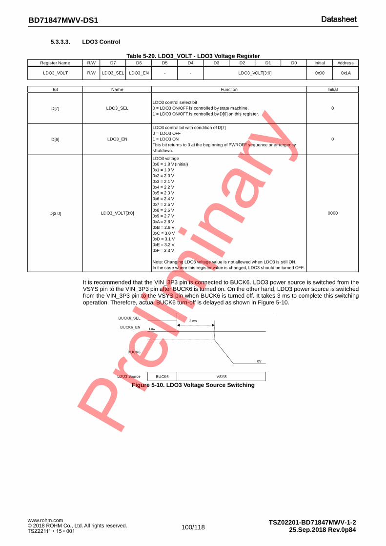
100/118 25.Sep.2018 Rev.0p84 © 2018 ROHM Co., Ltd. All rights reserved. www.rohm.com
TSZ22111 • 15 • 001
TSZ02201-BD71847MWV-1-2
BD71847MWV-DS1
5.3.3.3. LDO3 Control
Table 5-29. LDO3_VOLT - LDO3 Voltage Register
It is recommended that the VIN_3P3 pin is connected to BUCK6. LDO3 power source is switched from the VSYS pin to the VIN_3P3 pin after BUCK6 is turned on. On the other hand, LDO3 power source is switched from the VIN_3P3 pin to the VSYS pin when BUCK6 is turned off. It takes 3 ms to complete this switching operation. Therefore, actual BUCK6 turn-off is delayed as shown in Figure 5-10.
Figure 5-10. LDO3 Voltage Source Switching
Register Name R/W D7 D6 D5 D4 D3 D2 D1 D0 Initial Address
LDO3_VOLT R/W LDO3_SEL LDO3_EN - - 0x00 0x1A
Bit
D[7]
D[6]
D[3:0] LDO3_VOLT[3:0]
LDO3 voltage
0x0 = 1.8 V (Initial)
0x1 = 1.9 V
0x2 = 2.0 V
0x3 = 2.1 V
0x4 = 2.2 V
0x5 = 2.3 V
0x6 = 2.4 V
0x7 = 2.5 V
0x8 = 2.6 V
0x9 = 2.7 V
0xA = 2.8 V
0xB = 2.9 V
0xC = 3.0 V
0xD = 3.1 V
0xE = 3.2 V
0xF = 3.3 V
Note: Changing LDO3 voltage value is not allowed when LDO3 is still ON.
In the case where this register value is changed, LDO3 should be turned OFF.
0000
LDO3_VOLT[3:0]
Name Function Initial
LDO3_SEL
LDO3_EN
LDO3 control select bit
0 = LDO3 ON/OFF is controlled by state machine.
1 = LDO3 ON/OFF is controlled by D[6] on this register.
LDO3 control bit with condition of D[7]
0 = LDO3 OFF
1 = LDO3 ON
This bit returns to 0 at the beginning of PWROFF sequence or emergency
shutdown.
0
0
BUCK6_SEL
BUCK6_EN Low
3 ms
BUCK6
VSYSBUCK6LDO3 Source
0V

101/118 25.Sep.2018 Rev.0p84 © 2018 ROHM Co., Ltd. All rights reserved. www.rohm.com
TSZ22111 • 15 • 001
TSZ02201-BD71847MWV-1-2
BD71847MWV-DS1
5.3.4. LDO4
5.3.4.1. LDO4 Block Diagram
Figure 5-11. LDO4 Block Diagram
VSYS
VSYS
COLDO4
-Soft Start
+
-
DAC
VR FaultDetector
GND
OCP
VR Fault S ignal
Voltage set ting
E N
LDO4_VOUT
VREF
VR Controller
Discharge
Resistor
PGND
(EXP-PAD)
VIN_1P8_1
LDO4_FB
EN
Note : The source of LDO4 is VSYS when BUCK7 is OFF. The source of LDO4 is VIN_1P8_1 when BUCK7 is ON. The changing of the source is automatic.
BUCK7

102/118 25.Sep.2018 Rev.0p84 © 2018 ROHM Co., Ltd. All rights reserved. www.rohm.com
TSZ22111 • 15 • 001
TSZ02201-BD71847MWV-1-2
BD71847MWV-DS1
5.3.4.2. LDO4 Electrical Characteristics
Table 5-30. LDO4 Electrical Characteristics
Min Typ Max
Output Voltage VO_LDO4 0.885 0.900 0.915 VVO=0.9 V setting
Io=1 mA
Output Voltage Range VORG_LDO4 0.900 - 1.800 V 100 mV step
Maximum Output Current IOMAX_LDO4 250 - - mA
Over Current Protection IOCP_LDO4 325 - - mA
Quiescent Current IQ_LDO4 - 9 - µA Io = 0 mA
Dropout Voltage ΔVODP_LDO4 - 450 - mVIo = Iomax
VIN_V1P8_1 = 1.7 V, VO = 1.8 V setting
Start up Time tST_LDO4 - 400 1000 µsIo = 0 mA,
During EN to 90% of nominal Voltage
DC Output Voltage Load Regulation ΔVLDR_LDO4 - 10 20 mV Io = 1 mA to Iomax
DC Output Voltage Line Regulation ΔVLNR_LDO4 - 2 5 mV VSYS = 4.5 V to 5.5 V, Io = 50 mA
Discharge Resistance RDIS_LDO4 - 100 200 Ω
VR Fault Detect Level DVRFLDO4 - 80 - %Output = Sweep down
Power good detect level / Vo x 100
VR Fault Detect Hysteresis DVRFLDO4_HYS - 10 - %(VR fault release level - detect level) / Vo x
100
Ripple Rejection Ratio RRLDO4 - 60 - dB
VSYS = 5.0 V, IO=Iomax/2
VR = -20 dBV, fR=100 Hz
BW=20 Hz to 20 kHz
Output Capacitance COLDO4 1.1 2.2 22.0 μFTa = -40°C to +85°C,
effective capacitance with LDO's DC bias
(Unless otherwise specified, Ta = +25 °C, VSYS = 5.0 V, VIN_3P3 = 3.3 V, VIN_1P8_1 = 1.8 V, Vo = 0.9 V setting)
Parameter SymbolLimit
Unit Condition

103/118 25.Sep.2018 Rev.0p84 © 2018 ROHM Co., Ltd. All rights reserved. www.rohm.com
TSZ22111 • 15 • 001
TSZ02201-BD71847MWV-1-2
BD71847MWV-DS1
5.3.4.3. LDO4 Control
Table 5-31. LDO4_VOLT - LDO4 Voltage Register
It is recommended that the VIN_1P8_1 pin is connected to BUCK7. LDO4 power source is switched from the VSYS pin to the VIN_1P8_1 pin after BUCK7 is turned on. On the other hand, LDO4 power source is switched from the VIN_1P8_1 pin to the VSYS pin when BUCK7 is turned off. It takes 3 ms to complete this switching operation. Therefore, actual BUCK7 turn-off is delayed as shown in Figure 5-12.
Figure 5-12. LDO4 Voltage Source Switching
Register Name R/W D7 D6 D5 D4 D3 D2 D1 D0 Initial Address
LDO4_VOLT R/W LDO4_SEL LDO4_EN - - 0x00 0x1B
Bit
D[7]
D[6]
D[3:0] LDO4_VOLT[3:0]
LDO4 voltage
0x0 = 0.9 V (Initial)
0x1 = 1.0 V
0x2 = 1.1 V
0x3 = 1.2 V
0x4 = 1.3 V
0x5 = 1.4 V
0x6 = 1.5 V
0x7 = 1.6 V
0x8 = 1.7 V
0x9 = 1.8 V
0xA = 1.8 V
0xB = 1.8 V
0xC = 1.8 V
0xD= 1.8 V
0xE = 1.8 V
0xF = 1.8 V
Note: Changing LDO4 voltage value is not allowed when LDO4 is still ON.
In the case where this register value is changed, LDO4 should be turned OFF.
0000
LDO4_VOLT[3:0]
Name Function Initial
LDO4_SEL
LDO4_EN
LDO4 control select bit
0 = LDO4 ON/OFF is controlled by state machine.
1 = LDO4 ON/OFF is controlled by D[6] on this register.
LDO4 control bit with condition of D[7]
0 = LDO4 OFF
1 = LDO4 ON
This bit returns to 0 at the beginning of PWROFF sequence or emergency
shutdown.
0
0
BUCK7_SEL
BUCK7_EN Low
3 ms
BUCK7
VSYSBUCK7LDO4 Source
0V

104/118 25.Sep.2018 Rev.0p84 © 2018 ROHM Co., Ltd. All rights reserved. www.rohm.com
TSZ22111 • 15 • 001
TSZ02201-BD71847MWV-1-2
BD71847MWV-DS1
5.3.5. LDO5
5.3.5.1. LDO5 Block Diagram
Figure 5-13. LDO5 Block Diagram
VSYS
VSYS
COLDO5
-Soft Start
+
-
DAC
VR FaultDetector
GND
OCP
VR Fault S ignal
Voltage set ting
EN
LDO5_VOUT
VREF
VR ControllerDischarge
Resistor
PGND
(EX P-PAD)
EN

105/118 25.Sep.2018 Rev.0p84 © 2018 ROHM Co., Ltd. All rights reserved. www.rohm.com
TSZ22111 • 15 • 001
TSZ02201-BD71847MWV-1-2
BD71847MWV-DS1
5.3.5.2. LDO5 Electrical Characteristics
Table 5-32. LDO5 Electrical Characteristics
Min Typ Max
Output Voltage VO_LDO5 3.267 3.300 3.333 VVO=3.3 V setting
Io=1 mA
Output Voltage Range VORG_LDO5 0.800 - 3.300 V 100 mV step
Maximum Output Current IOMAX_LDO5 300 - - mA
Over Current Protection IOCP_LDO5 340 - - mA
Quiescent Current IQ_LDO5 - 9 - µA Io = 0 mA
Dropout Voltage ΔVODP_LDO5 - 250 - mVIo = Iomax
VSYS = 3.2 V, VO = 3.3 V setting
Start up Time tST_LDO5 - 530 1000 µsIo = 0 mA,
During EN to 90% of nominal Voltage
DC Output Voltage Load Regulation ΔVLDR_LDO5 - 10 20 mV Io = 1 mA to Iomax
DC Output Voltage Line Regulation ΔVLNR_LDO5 - 2 5 mV VSYS = 4.5 V to 5.5 V, Io = 50 mA
Discharge Resistance RDIS_LDO5 - 100 200 Ω
VR Fault Detect Level DVRFLDO5 - 80 - %Output = Sweep down
Power good detect level / Vo x 100
VR Fault Detect Hysteresis DVRFLDO5_HYS - 10 - %(VR fault release level - detect level) / Vo x
100
Ripple Rejection Ratio RRLDO5 - 60 - dB
VSYS = 5.0 V, IO=Iomax/2
VR = -20 dBV, fR=100 Hz
BW=20 Hz to 20 kHz
Output Capacitance COLDO5 1.1 2.2 22.0 μFTa = -40°C to +85°C,
effective capacitance with LDO's DC bias
(Unless otherwise specified, Ta = +25 °C, VSYS = 5.0 V, VIN_3P3 = 3.3 V, VIN_1P8_1 = 1.8 V, Vo = 3.3 V setting)
Parameter SymbolLimit
Unit Condition

106/118 25.Sep.2018 Rev.0p84 © 2018 ROHM Co., Ltd. All rights reserved. www.rohm.com
TSZ22111 • 15 • 001
TSZ02201-BD71847MWV-1-2
BD71847MWV-DS1
5.3.5.3. LDO5 Control
Table 5-33. LDO5_VOLT - LDO5 Voltage Register
Register Name R/W D7 D6 D5 D4 D3 D2 D1 D0 Initial Address
LDO5_VOLT R/W LDO5_SEL LDO5_ENLDO5_VOL
T_SEL- 0x8F 0x1C
Bit
D[7]
D[6]
D[5]
D[3:0]
LDO5_VOLT[3:0]
Name Function Initial
LDO5_VOLT[3:0]
LDO5 voltage
if D[5]=0,
0x0 = 1.8 V 0x1 = 1.9 V 0x2 = 2.0 V 0x3 = 2.1 V
0x4 = 2.2 V 0x5 = 2.3 V 0x6 = 2.4 V 0x7 = 2.5 V
0x8 = 2.6 V 0x9 = 2.7 V 0xA = 2.8 V 0xB = 2.9 V
0xC = 3.0 V 0xD= 3.1 V 0xE = 3.2 V 0xF = 3.3 V(initial)
if D[5]=1,
0x0 = 0.8 V 0x1 = 0.9 V 0x2 = 1.0 V 0x3 = 1.1 V
0x4 = 1.2 V 0x5 = 1.3 V 0x6 = 1.4 V 0x7 = 1.5 V
0x8 = 1.6 V 0x9 = 1.7 V 0xA = 1.8 V 0xB = 1.9 V
0xC = 2.0 V 0xD= 2.1 V 0xE = 2.2 V 0xF = 2.3 V
Note: Changing LDO5 voltage value is not allowed when LDO5 is still ON.
In the case where this register value is changed, LDO5 should be turned OFF.
1111
LDO5_EN
LDO5 control bit with condition of D[7]
0 = LDO5 OFF
1 = LDO5 ON
This bit returns to 0 at the beginning of PWROFF sequence or emergency
shutdown.
0
LDO5_SEL
LDO5 control select bit
0 = LDO5 ON/OFF is controlled by state machine.
1 = LDO5 ON/OFF is controlled by D[6] on this register.
1
LDO5_VOLT_SEL
Select the LDO5 voltage range set by D[1:0].
0 = 1.8 V to 3.3 V
1 = 0.8 V to 2.3 V
Note: Changing LDO5 voltage value is not allowed when LDO5 is still ON.
In the case where this register value is changed, LDO5 should be turned OFF.
0
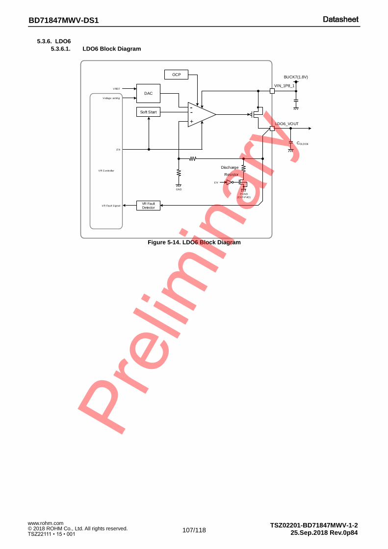
107/118 25.Sep.2018 Rev.0p84 © 2018 ROHM Co., Ltd. All rights reserved. www.rohm.com
TSZ22111 • 15 • 001
TSZ02201-BD71847MWV-1-2
BD71847MWV-DS1
5.3.6. LDO6
5.3.6.1. LDO6 Block Diagram
Figure 5-14. LDO6 Block Diagram
VIN_1P8_1
BUCK7(1.8V)
COLDO6
-Soft Start
+
-
DAC
VR FaultDetector
GND
OCP
VR Fault S ignal
Voltage set ting
EN
LDO6_VOUT
VREF
VR ControllerDischarge
Resistor
PGND
(EX P-PAD)
EN

108/118 25.Sep.2018 Rev.0p84 © 2018 ROHM Co., Ltd. All rights reserved. www.rohm.com
TSZ22111 • 15 • 001
TSZ02201-BD71847MWV-1-2
BD71847MWV-DS1
5.3.6.2. LDO6 Electrical Characteristics
Table 5-34. LDO6 Electrical Characteristics
Min Typ Max
Output Voltage VO_LDO6 1.185 1.200 1.215 VVO=1.2 V setting
Io=1 mA
Output Voltage Range VORG_LDO6 0.900 - 1.800 V 100 mV step
Maximum Output Current IOMAX_LDO6 300 - - mA
Over Current Protection IOCP_LDO6 340 - - mA
Quiescent Current IQ_LDO6 - 9 - µA Io = 0 mA
Dropout Voltage ΔVODP_LDO6 - 450 - mVIo = Iomax
VIN_V1P8_1 = 1.7 V, VO = 1.8 V setting
Start up Time tST_LDO6 - 400 1000 µsIo = 0 mA,
During EN to 90% of nominal Voltage
DC Output Voltage Load Regulation ΔVLDR_LDO6 - 10 20 mV Io = 1 mA to Iomax
DC Output Voltage Line Regulation ΔVLNR_LDO6 - 2 5 mV VSYS = 4.5 V to 5.5 V, Io = 50 mA
Discharge Resistance RDIS_LDO6 - 100 200 Ω
VR Fault Detect Level DVRFLDO6 - 80 - %Output = Sweep down
Power good detect level / Vo x 100
VR Fault Detect Hysteresis DVRFLDO6_HYS - 10 - %(VR fault release level - detect level) / Vo x
100
Ripple Rejection Ratio RRLDO6 - 60 - dB
VSYS = 5.0 V, IO=Iomax/2
VR = -20 dBV, fR=100 Hz
BW=20 Hz to 20 kHz
Output Capacitance COLDO6 1.1 2.2 22.0 μFTa = -40°C to +85°C,
effective capacitance with LDO's DC bias
(Unless otherwise specified, Ta = +25 °C, VSYS = 5.0 V, VIN_3P3 = 3.3 V, VIN_1P8_1 = 1.8 V, Vo = 1.2 V setting)
Parameter SymbolLimit
Unit Condition

109/118 25.Sep.2018 Rev.0p84 © 2018 ROHM Co., Ltd. All rights reserved. www.rohm.com
TSZ22111 • 15 • 001
TSZ02201-BD71847MWV-1-2
BD71847MWV-DS1
5.3.6.3. LDO6 Control
Table 5-35. LDO6_VOLT - LDO6 Voltage Register
Register Name R/W D7 D6 D5 D4 D3 D2 D1 D0 Initial Address
LDO6_VOLT R/W LDO6_SEL LDO6_EN - - 0x03 0x1D
Bit
D[7]
D[6]
D[3:0]
LDO6_VOLT[3:0]
Name Function Initial
LDO6_VOLT[3:0]
LDO6 voltage
0x0 = 0.9 V
0x1 = 1.0 V
0x2 = 1.1 V
0x3 = 1.2 V (initial)
0x4 = 1.3 V
0x5 = 1.4 V
0x6 = 1.5 V
0x7 = 1.6 V
0x8 = 1.7 V
0x9 = 1.8 V
0xA = 1.8 V
0xB = 1.8 V
0xC = 1.8 V
0xD= 1.8 V
0xE = 1.8 V
0xF = 1.8 V
Note: Changing LDO6 voltage value is not allowed when LDO6 is still ON.
In the case where this register value is changed, LDO6 should be turned OFF.
0011
LDO6_EN
LDO6 control bit with condition of D[7]
0 = LDO6 OFF
1 = LDO6 ON
This bit returns to 0 at the beginning of PWROFF sequence or emergency
shutdown.
0
LDO6_SEL
LDO6 control select bit
0 = LDO6 ON/OFF is controlled by state machine.
1 = LDO6 ON/OFF is controlled by D[6] on this register.
0

110/118 25.Sep.2018 Rev.0p84 © 2018 ROHM Co., Ltd. All rights reserved. www.rohm.com
TSZ22111 • 15 • 001
TSZ02201-BD71847MWV-1-2
BD71847MWV-DS1
5.4. MUXSW
MUX Switch is for SD card power.
5.4.1. MUXSW Block Diagram
Figure 5-15. MUXSW Block Diagram
VIN_3P3
BUCK6
COMUXSW
PGND
(EXP-PAD)
MUXSW_VOUTMUX
Switch
Controller
VIN_1P8_2
SD_VSELECT
BUCK7
DISCHARGE
RESISTOR
DVDD
MUXSW_EN

111/118 25.Sep.2018 Rev.0p84 © 2018 ROHM Co., Ltd. All rights reserved. www.rohm.com
TSZ22111 • 15 • 001
TSZ02201-BD71847MWV-1-2
BD71847MWV-DS1
5.4.2. MUXSW Electrical Characteristics
Table 5-36. MUXSW Electrical Characteristics
Table 5-37. SD_VSELECT Electrical Characteristics
Figure 5-16. MUXSW Sequence
Table 5-38. MUXSW Sequence Timing
Table 5-39. MUXSW_EN - MUXSW Enable Register
Min Typ Max
VIN_3P3 Input Voltage VIN_3P3 - 3.300 - V
Switch ON Resistance(3.3V mode) RON_3P3 - - 500 mΩ SD_VSELECT=0 V, VIN_3P3>3.2 V
VIN_1P8_2 Input Voltage VIN_1P8 - 1.800 - V
Switch ON Resistance(1.8V mode) RON_1P8 - - 500 mΩ SD_VSELECT=DVDD, VIN_1P8_2>1.7 V
Maximum Output Current IOMAX_MUX 150 - - mA
Discharge Resistance RDIS_MUX - 30 50 Ω VIN_1P8_2=0 V, VIN_3P3=0 V, IO=-10 mA
Output Capacitance CO_MUX 11 22 33 μFTa=-40°C to +85°C,
effective capacitance with Output voltage
(Unless otherwise specified, Ta = +25 °C, VSYS = 5.0 V, VIN_3P3 = 3.3 V, VIN_1P8_2 = 1.8 V, Vo = 3.3 V setting)
Parameter SymbolLimit
Unit Condition
Min Typ Max
Input "H" Level VIHSDV
DVDD
x 0.75- - V
Input "L" Level VILSDV - -DVDD
x 0.25V
(Unless otherwise specified, Ta=25°C, DVDD=1.8 V)
Parameter SymbolLimit
Unit Condition
SD_VSELECT
t1
MUXSW_VOUT
3.30 V 3.30 V
1.89 V
1.80 V
3.15 V
t2
trtf
Symbol Description Min Typ Max Unit
t1 SD_VSELCT High Time(Note 1) 2 - - ms
t2 SD_VSELCT Low Time(Note 1) 2 - - ms
tf Transition Time 3.3 V to 1.8 V - - 1 ms
tr Transition Time 1.8 V to 3.3 V - - 1 ms
(Note 1) t1 and t2 need ov er 2ms.
Register Name R/W D7 D6 D5 D4 D3 D2 D1 D0 Initial Address
MUXSW_EN R/W - - - - - - - MUXSW_EN 0x01 0x30
Bit
D[0]
Name Function Initial
MUXSW_EN
MUXSW control bit
0 = MUXSW OFF
1 = MUXSW ON
1

112/118 25.Sep.2018 Rev.0p84 © 2018 ROHM Co., Ltd. All rights reserved. www.rohm.com
TSZ22111 • 15 • 001
TSZ02201-BD71847MWV-1-2
BD71847MWV-DS1
6. 32.768 kHz Crystal Oscillator Driver 6.1. 32.768 kHz Crystal Oscillator Driver Block Diagram
Figure 6-1. 32.768 kHz Crystal Oscillator Driver Block Diagram
Table 6-1. C32K_OUT Control Register
At the beginning of power-on, the C32K_OUT pin output clock is generated from the 12-MHz internal oscillator; the clock frequency is equal to 12 MHz / 375. If an external 32.768 kHz crystal is present, the C32K_OUT pin output clock’s clock source is switched from the internal oscillator to the crystal clock after 3000 crystal clock cycles, i.e., it is assumed that the crystal clock is stable by then.
6.2. 32.768 kHz Crystal Oscillator Driver Electrical Characteristics
Table 6-2. 32.768 kHz Crystal Oscillator Driver Electrical Characteristics
Oscillator Driver
CONTROLLER
C32K_OUT
INTLDO1P5
XIN
XOUT
32.768kHz
Crystal
OUT32K_EN
DVDD
VDD_V1P5
VDD_V1P5
VDD_V1P5
Counter
M
U
X
12MHz
1/375
divider
Register Name R/W D7 D6 D5 D4 D3 D2 D1 D0 Initial Address
OUT32K R/W - - - - - - - OUT32K_EN 0x01 0x2E
Bit
D[0] OUT32K_EN0 = Disable (C32K_OUT is Low level)
1 = Enable1
Name Function Initial
Min Typ Max
Output Frequency fRTCLK - 32.768 - kHz With external crystal
Output Duty Cycle 40 50 60 %
Output H Level Voltage VOH32K
DVDD
x 0.8- - V IOH = -1 mA
Output L Level Voltage VOL32K - - 0.4 V IOL = 1 mA
ST3215SB32768H5HPWAA (KYOCERA: CL=12.5pF)
(Note) The f ollowing 32.768 kHz cry stal is recommended.
(Unless otherwise specified, Ta = +25°C, VSYS = 5.0 V, DVDD = 1.8 V)
Parameter SymbolLimit
Unit Condition

113/118 25.Sep.2018 Rev.0p84 © 2018 ROHM Co., Ltd. All rights reserved. www.rohm.com
TSZ22111 • 15 • 001
TSZ02201-BD71847MWV-1-2
BD71847MWV-DS1
7. Operational Notes
1. Reverse Connection of Power Supply
Connecting the power supply in reverse polarity can damage the IC. Take precautions against reverse polarity when connecting the power supply, such as mounting an external diode between the power supply and the IC’s power supply pins.
2. Power Supply Lines
Design the PCB layout pattern to provide low impedance supply lines. Separate the ground and supply lines of the digital and analog blocks to prevent noise in the ground and supply lines of the digital block from affecting the analog block. Furthermore, connect a capacitor to ground at all power supply pins. Consider the effect of temperature and aging on the capacitance value when using electrolytic capacitors.
3. Ground Voltage
Ensure that no pins are at a voltage below that of the ground pin at any time, even during transient condition.
4. Ground Wiring Pattern
When using both small-signal and large-current ground traces, the two ground traces should be routed separately but connected to a single ground at the reference point of the application board to avoid fluctuations in the small-signal ground caused by large currents. Also ensure that the ground traces of external components do not cause variations on the ground voltage. The ground lines must be as short and thick as possible to reduce line impedance.
5. Recommended Operating Conditions
The function and operation of the IC are guaranteed within the range specified by the recommended operating conditions. The characteristic values are guaranteed only under the conditions of each item specified by the electrical characteristics.
6. Inrush Current
When power is first supplied to the IC, it is possible that the internal logic may be unstable and inrush current may flow instantaneously due to the internal powering sequence and delays, especially if the IC has more than one power supply. Therefore, give special consideration to power coupling capacitance, power wiring, width of ground wiring, and routing of connections.
7. Operation Under Strong Electromagnetic Field
Operating the IC in the presence of a strong electromagnetic field may cause the IC to malfunction.
8. Testing on Application Boards
When testing the IC on an application board, connecting a capacitor directly to a low-impedance output pin may subject the IC to stress. Always discharge capacitors completely after each process or step. The IC’s power supply should always be turned off completely before connecting or removing it from the test setup during the inspection process. To prevent damage from static discharge, ground the IC during assembly and use similar precautions during transport and storage.
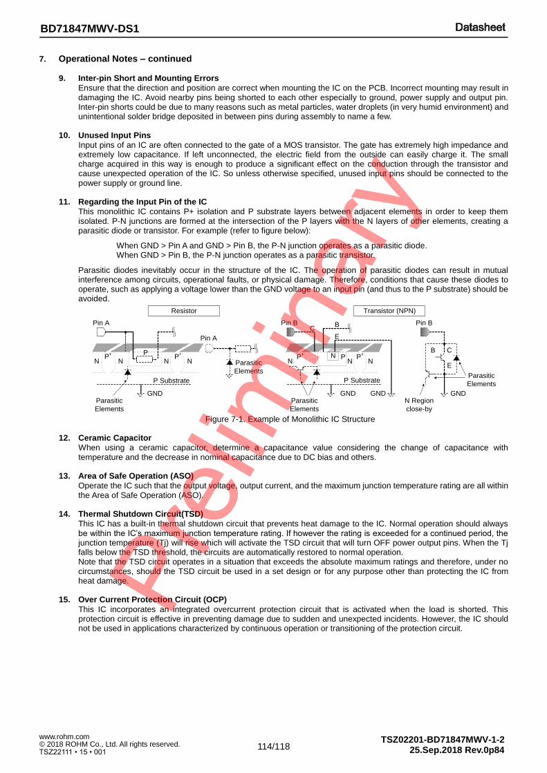
114/118 25.Sep.2018 Rev.0p84 © 2018 ROHM Co., Ltd. All rights reserved. www.rohm.com
TSZ22111 • 15 • 001
TSZ02201-BD71847MWV-1-2
BD71847MWV-DS1
7. Operational Notes – continued
9. Inter-pin Short and Mounting Errors
Ensure that the direction and position are correct when mounting the IC on the PCB. Incorrect mounting may result in damaging the IC. Avoid nearby pins being shorted to each other especially to ground, power supply and output pin. Inter-pin shorts could be due to many reasons such as metal particles, water droplets (in very humid environment) and unintentional solder bridge deposited in between pins during assembly to name a few.
10. Unused Input Pins
Input pins of an IC are often connected to the gate of a MOS transistor. The gate has extremely high impedance and extremely low capacitance. If left unconnected, the electric field from the outside can easily charge it. The small charge acquired in this way is enough to produce a significant effect on the conduction through the transistor and cause unexpected operation of the IC. So unless otherwise specified, unused input pins should be connected to the power supply or ground line.
11. Regarding the Input Pin of the IC
This monolithic IC contains P+ isolation and P substrate layers between adjacent elements in order to keep them isolated. P-N junctions are formed at the intersection of the P layers with the N layers of other elements, creating a parasitic diode or transistor. For example (refer to figure below):
When GND > Pin A and GND > Pin B, the P-N junction operates as a parasitic diode. When GND > Pin B, the P-N junction operates as a parasitic transistor.
Parasitic diodes inevitably occur in the structure of the IC. The operation of parasitic diodes can result in mutual interference among circuits, operational faults, or physical damage. Therefore, conditions that cause these diodes to operate, such as applying a voltage lower than the GND voltage to an input pin (and thus to the P substrate) should be avoided.
Figure 7-1. Example of Monolithic IC Structure
12. Ceramic Capacitor
When using a ceramic capacitor, determine a capacitance value considering the change of capacitance with temperature and the decrease in nominal capacitance due to DC bias and others.
13. Area of Safe Operation (ASO)
Operate the IC such that the output voltage, output current, and the maximum junction temperature rating are all within the Area of Safe Operation (ASO).
14. Thermal Shutdown Circuit(TSD)
This IC has a built-in thermal shutdown circuit that prevents heat damage to the IC. Normal operation should always be within the IC’s maximum junction temperature rating. If however the rating is exceeded for a continued period, the junction temperature (Tj) will rise which will activate the TSD circuit that will turn OFF power output pins. When the Tj falls below the TSD threshold, the circuits are automatically restored to normal operation. Note that the TSD circuit operates in a situation that exceeds the absolute maximum ratings and therefore, under no circumstances, should the TSD circuit be used in a set design or for any purpose other than protecting the IC from heat damage.
15. Over Current Protection Circuit (OCP)
This IC incorporates an integrated overcurrent protection circuit that is activated when the load is shorted. This protection circuit is effective in preventing damage due to sudden and unexpected incidents. However, the IC should not be used in applications characterized by continuous operation or transitioning of the protection circuit.
N NP
+ P
N NP
+
P Substrate
GND
NP
+
N NP
+N P
P Substrate
GND GND
Parasitic
Elements
Pin A
Pin A
Pin B Pin B
B C
E
Parasitic
Elements
GNDParasitic
Elements
CB
E
Transistor (NPN)Resistor
N Region
close-by
Parasitic
Elements

115/118 25.Sep.2018 Rev.0p84 © 2018 ROHM Co., Ltd. All rights reserved. www.rohm.com
TSZ22111 • 15 • 001
TSZ02201-BD71847MWV-1-2
BD71847MWV-DS1
8. Ordering Information
B D 7 1 8 4 7 M W V - E 2
Part Number
Package MWV: UQFN56BV7070
Packaging and forming specification E2: Embossed tape and reel
9. Marking Diagram
Figure 9-1. Marking Diagram
UQFN56BV7070 (TOP VIEW)
BD71847
Part Number Marking
LOT Number
Pin 1 Mark
A0 0000
ROHM

116/118 25.Sep.2018 Rev.0p84 © 2018 ROHM Co., Ltd. All rights reserved. www.rohm.com
TSZ22111 • 15 • 001
TSZ02201-BD71847MWV-1-2
BD71847MWV-DS1
10. Physical Dimension and Packing Information
Package Name UQFN56BV7070

117/118 25.Sep.2018 Rev.0p84 © 2018 ROHM Co., Ltd. All rights reserved. www.rohm.com
TSZ22111 • 15 • 001
TSZ02201-BD71847MWV-1-2
BD71847MWV-DS1
11. Revision History
Date Revision Number Description
12.Jan.2018 Rev.0p80 First Release
05.Feb.2018 Rev.0p81 The change of System Powermap (Figure 1-1)
05.Feb.2018 Rev.0p81 The change of Typical Application Circuit (Figure 1-2)
05.Feb.2018 Rev.0p81 The change of Pin configuration and Description (Figure 1-4, Table1-2)
05.Feb.2018 Rev.0p81 The change of G1_3 in Terminal Equivalent Circuit2(Figure 1-6)
05.Feb.2018 Rev.0p81 The change of the initial voltage and range in Power Rail(Table 1-3)
05.Feb.2018 Rev.0p81 The change of the Register Map(Table 1-4)
05.Feb.2018 Rev.0p81 The change of the OTP Version Register(Table 1-7)
05.Feb.2018 Rev.0p81 The change of the Power State(Table 3-8)
05.Feb.2018 Rev.0p81 The change of the Sequence(Table3-38 to 3-46, Fig3-21 to Fig3-29)
05.Feb.2018 Rev.0p81 The change of the output voltage range(Table 5-1)
05.Feb.2018 Rev.0p81 The change of the ourput voltage in BUC2 Electrical Characteristic(Table 5-8)
05.Feb.2018 Rev.0p81 The change of the initial value in BUCK2_VOLT_RUN Voltage Register(Table 5-10)
05.Feb.2018 Rev.0p81 The change of the ourput voltage in BUC5 Electrical Characteristic(Table 5-12)
05.Feb.2018 Rev.0p81 The change of the initial value in BUCK5_VOLT Voltage Register(Table 5-14)
05.Feb.2018 Rev.0p81 The change of the ourput voltage in LDO4 Electrical Characteristic(Table 5-30)
05.Feb.2018 Rev.0p81 The change of the initial value in LDO4 Voltage Register(Table 5-31)
05.Feb.2018 Rev.0p81 The change of the VSOURCE in LDO5 (Figure 5-13)
05.Feb.2018 Rev.0p81The change of the ourput voltage and range and Droop Voltage and OCP Maxmum output Current in LDO5
Electrical Characteristic(Table 5-32)
05.Feb.2018 Rev.0p81 The change of the LDO5 Voltage Register(Table 5-33)
05.Feb.2018 Rev.0p81 The change of the ourput voltage in LDO6 Electrical Characteristic(Table 5-34)
05.Feb.2018 Rev.0p81 The change of the initial value in LDO5 Voltage Register(Table 5-35)
09.Mar.2018 Rev.0p82Updated Table 3-34(Initaila Value)
<Rev.0p81> 04 <Rev.0p82> CF
09.Mar.2018 Rev.0p82Updated Table 1-4(Initaila Value:Address20)
<Rev.0p81> 04 <Rev.0p82> CF
09.Mar.2018 Rev.0p82
Updated Table5-4, 5-9, 5-13, 5-16, 5-19, 5-22
Deleted the below comment in D[1]
"This bit returns to 0 at the end of PWROFF sequence or emergency shutdown."
09.Mar.2018 Rev.0p82
Updated Table5-4, 5-9, 5-13, 5-16, 5-19, 5-22
Changed the below comment in D[2]
<Rev.0p81>
"This bit returns to 0 at the end of PWROFF sequence or emergency shutdown."
<Rev.0p82>
"This bit returns to 0 at the beginning of PWROFF sequence or emergency shutdown."
09.Mar.2018 Rev.0p82
Updated Table5-25, 5-27, 5-29, 5-31, 5-33, 5-35
Deleted the below comment in D[7]
"This bit returns to 0 at the end of PWROFF sequence or emergency shutdown."
09.Mar.2018 Rev.0p82
Updated Table5-25, 5-27, 5-29, 5-31, 5-33, 5-35
Changed the below comment in D[6]
<Rev.0p81>
"This bit returns to 0 at the end of PWROFF sequence or emergency shutdown."
<Rev.0p82>
"This bit returns to 0 at the beginning of PWROFF sequence or emergency shutdown."
09.Mar.2018 Rev.0p82
Added the below comment in Table 5-14,17,20,23,25,27,29,31,33,35
(Bit Name: xxx_VOLT_SEL, xxx_VOLT)
Note: Changing LDOx(BUCKx) voltage value is not allowed when LDOx(BUCKx) is still ON.
In the case where this register value is changed, LDOx(BUCKx) should be turned OFF.
09.Mar.2018 Rev.0p82
Updated the Table3-23 (BUCK5 VR Fault in Supsend)
<Rev.0p81> -
<Rev.0p82>“80%<BUCK5<130%”
09.Mar.2018 Rev.0p82
Updated the Features(P1)
<Rev.0p81> Buck 5: 3.0A, 0.7V to 1.35V/8steps DVS
<Rev.0p82> Buck 5: 3.0A, 0.7V to 1.35V/8steps
09.Mar.2018 Rev.0p82
Change DVDD operating ratings range
<Rev.0p81> 2.70V to 3.60V
<Rev.0p82> 1.71V to 5.50V
09.Mar.2018 Rev.0p82
Change PWRON_B connection when not use power button (Figure 1-2)
<Rev.0p81> Connect to GND
<Rev.0p82> Connect to VSYS
09.Mar.2018 Rev.0p82
Change PCB type (page 1 Features)
<Rev.0p81> 4-layer PCB
<Rev.0p82> Type 3 PCB applicable
09.Mar.2018 Rev.0p82 Change P/N to BD71847MWV-DS1
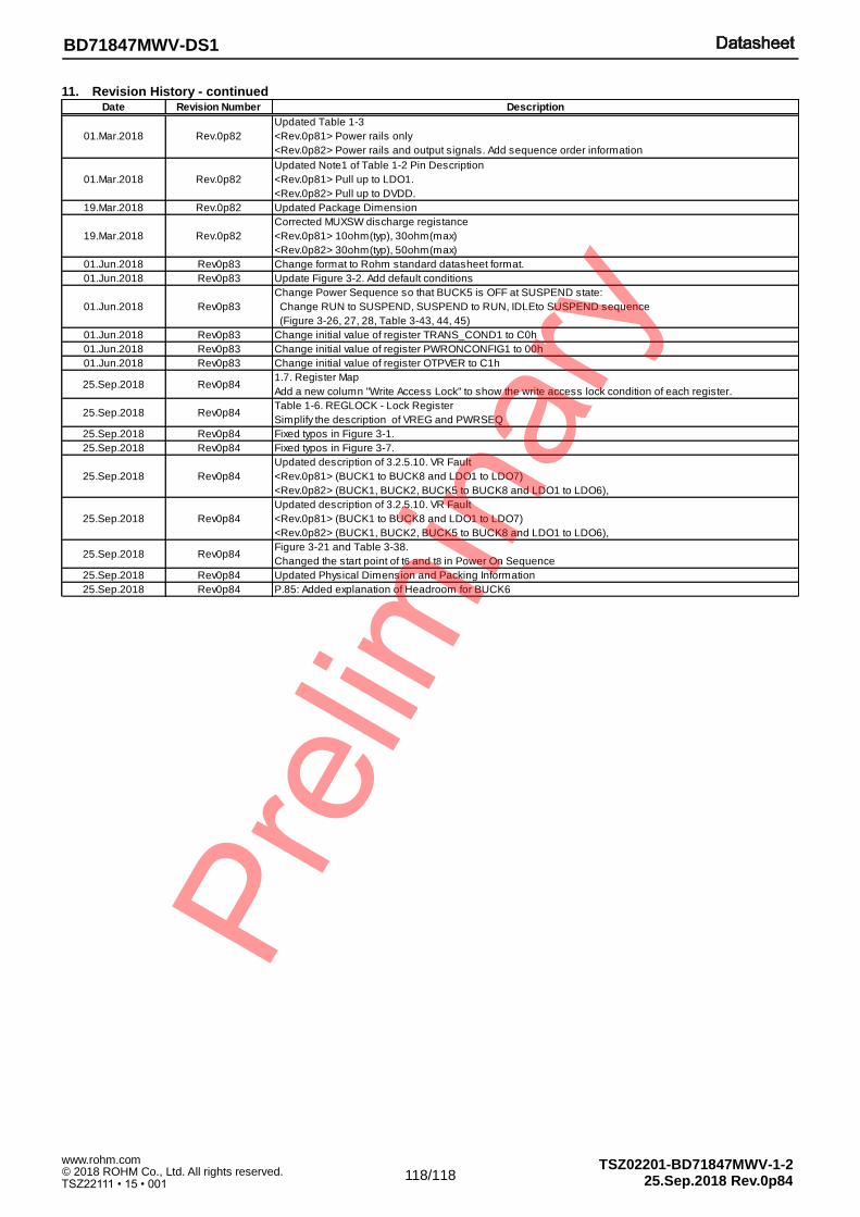
118/118 25.Sep.2018 Rev.0p84 © 2018 ROHM Co., Ltd. All rights reserved. www.rohm.com
TSZ22111 • 15 • 001
TSZ02201-BD71847MWV-1-2
BD71847MWV-DS1
11. Revision History - continued
Date Revision Number Description
01.Mar.2018 Rev.0p82
Updated Table 1-3
<Rev.0p81> Power rails only
<Rev.0p82> Power rails and output signals. Add sequence order information
01.Mar.2018 Rev.0p82
Updated Note1 of Table 1-2 Pin Description
<Rev.0p81> Pull up to LDO1.
<Rev.0p82> Pull up to DVDD.
19.Mar.2018 Rev.0p82 Updated Package Dimension
19.Mar.2018 Rev.0p82
Corrected MUXSW discharge registance
<Rev.0p81> 10ohm(typ), 30ohm(max)
<Rev.0p82> 30ohm(typ), 50ohm(max)
01.Jun.2018 Rev0p83 Change format to Rohm standard datasheet format.
01.Jun.2018 Rev0p83 Update Figure 3-2. Add default conditions
01.Jun.2018 Rev0p83
Change Power Sequence so that BUCK5 is OFF at SUSPEND state:
Change RUN to SUSPEND, SUSPEND to RUN, IDLEto SUSPEND sequence
(Figure 3-26, 27, 28, Table 3-43, 44, 45)
01.Jun.2018 Rev0p83 Change initial value of register TRANS_COND1 to C0h
01.Jun.2018 Rev0p83 Change initial value of register PWRONCONFIG1 to 00h
01.Jun.2018 Rev0p83 Change initial value of register OTPVER to C1h
25.Sep.2018 Rev0p841.7. Register Map
Add a new column "Write Access Lock" to show the write access lock condition of each register.
25.Sep.2018 Rev0p84Table 1-6. REGLOCK - Lock Register
Simplify the description of VREG and PWRSEQ
25.Sep.2018 Rev0p84 Fixed typos in Figure 3-1.
25.Sep.2018 Rev0p84 Fixed typos in Figure 3-7.
25.Sep.2018 Rev0p84
Updated description of 3.2.5.10. VR Fault
<Rev.0p81> (BUCK1 to BUCK8 and LDO1 to LDO7)
<Rev.0p82> (BUCK1, BUCK2, BUCK5 to BUCK8 and LDO1 to LDO6),
25.Sep.2018 Rev0p84
Updated description of 3.2.5.10. VR Fault
<Rev.0p81> (BUCK1 to BUCK8 and LDO1 to LDO7)
<Rev.0p82> (BUCK1, BUCK2, BUCK5 to BUCK8 and LDO1 to LDO6),
25.Sep.2018 Rev0p84Figure 3-21 and Table 3-38.
Changed the start point of t6 and t8 in Power On Sequence
25.Sep.2018 Rev0p84 Updated Physical Dimension and Packing Information
25.Sep.2018 Rev0p84 P.85: Added explanation of Headroom for BUCK6