power management ic - 2 e-fuses, 2 switching regulators · device (pmic) that integrates 2 e-fuses...
TRANSCRIPT

This is information on a product in full production.
March 2016 DocID028805 Rev 3 1/58
STPMIC02
Power management IC - 2 E-fuses, 2 switching regulators
Datasheet - production data
Features
E-fuse 12 V
– Current limit
– Current monitor
– Soft-start with current limit
– Voltage clamp
– Dedicated thermal protection
E-fuse 5 V
– Current limit
– Reverse current protection
– Current monitor
– Soft-start with current limit
– Voltage clamp
– Dedicated thermal protection
0.9 V - 3.5 A switching regulator
– Soft-start
– Overcurrent
– Undervoltage monitor
– 6-bit margining
3.3 V - 300 mA switching regulator
– Soft-start
– Overcurrent
– Undervoltage monitor
– 5-bit margining
High speed I2C serial interface (3.4 MHz)
Temperature monitor and shutdown
Power disable function
Description
The STPMIC02 chip is a power management device (PMIC) that integrates 2 E-fuses and 2 switching regulators. The chip supports a high speed (3.4 MHz) serial interface with the I2C serial protocol. This interface is bidirectional allowing the microprocessor to set the functions and read status.
Table 1. Device summary
Order code Package Packing
STPMIC02VQFN 24-pin
with EPADTray
STPMIC02TRVQFN 24-pin
with EPADTape and reel 13”
www.st.com

Contents STPMIC02
2/58 DocID028805 Rev 3
Contents
1 Block diagram . . . . . . . . . . . . . . . . . . . . . . . . . . . . . . . . . . . . . . . . . . . . . . 5
2 Pin description and pinout . . . . . . . . . . . . . . . . . . . . . . . . . . . . . . . . . . . . 6
3 Functional description . . . . . . . . . . . . . . . . . . . . . . . . . . . . . . . . . . . . . . . 8
3.1 E-fuse 12 V . . . . . . . . . . . . . . . . . . . . . . . . . . . . . . . . . . . . . . . . . . . . . . . . 8
3.1.1 E-fuse 12 V current limit . . . . . . . . . . . . . . . . . . . . . . . . . . . . . . . . . . . . 10
3.1.2 E-fuse 12 V current monitor . . . . . . . . . . . . . . . . . . . . . . . . . . . . . . . . . . 11
3.2 E-fuse 5 V . . . . . . . . . . . . . . . . . . . . . . . . . . . . . . . . . . . . . . . . . . . . . . . . 12
3.2.1 E-fuse 5 V current limit . . . . . . . . . . . . . . . . . . . . . . . . . . . . . . . . . . . . . 13
3.2.2 E-fuse 5 V current monitor . . . . . . . . . . . . . . . . . . . . . . . . . . . . . . . . . . . 13
3.2.3 EF5ON function . . . . . . . . . . . . . . . . . . . . . . . . . . . . . . . . . . . . . . . . . . . 14
3.3 VR09 . . . . . . . . . . . . . . . . . . . . . . . . . . . . . . . . . . . . . . . . . . . . . . . . . . . . 16
3.3.1 VR09 low power mode . . . . . . . . . . . . . . . . . . . . . . . . . . . . . . . . . . . . . . 17
3.3.2 VR09 current limit . . . . . . . . . . . . . . . . . . . . . . . . . . . . . . . . . . . . . . . . . 17
3.3.3 FW enable/disable: VR09Dis, VR09MonDis and VR09Key bits . . . . . . 18
3.3.4 Power monitor functions . . . . . . . . . . . . . . . . . . . . . . . . . . . . . . . . . . . . 19
3.3.5 VR09 software control sequence . . . . . . . . . . . . . . . . . . . . . . . . . . . . . . 20
3.4 VR33 . . . . . . . . . . . . . . . . . . . . . . . . . . . . . . . . . . . . . . . . . . . . . . . . . . . . 20
3.4.1 VR33 low power mode . . . . . . . . . . . . . . . . . . . . . . . . . . . . . . . . . . . . . . 21
3.4.2 VR33 current limit . . . . . . . . . . . . . . . . . . . . . . . . . . . . . . . . . . . . . . . . . 21
3.4.3 VR33 full duty operation . . . . . . . . . . . . . . . . . . . . . . . . . . . . . . . . . . . . 21
3.4.4 Power monitor functions . . . . . . . . . . . . . . . . . . . . . . . . . . . . . . . . . . . . 21
3.5 AVDD internal supply . . . . . . . . . . . . . . . . . . . . . . . . . . . . . . . . . . . . . . . . 22
3.6 Temperature monitor . . . . . . . . . . . . . . . . . . . . . . . . . . . . . . . . . . . . . . . . 23
3.7 P3 power disable . . . . . . . . . . . . . . . . . . . . . . . . . . . . . . . . . . . . . . . . . . . 24
3.8 SINTn function . . . . . . . . . . . . . . . . . . . . . . . . . . . . . . . . . . . . . . . . . . . . . 24
3.9 I2C serial interface . . . . . . . . . . . . . . . . . . . . . . . . . . . . . . . . . . . . . . . . . . 24
3.9.1 Slave address . . . . . . . . . . . . . . . . . . . . . . . . . . . . . . . . . . . . . . . . . . . . 25
3.9.2 I2C functional operation . . . . . . . . . . . . . . . . . . . . . . . . . . . . . . . . . . . . . 25

DocID028805 Rev 3 3/58
STPMIC02 Contents
58
4 Register description and defaults . . . . . . . . . . . . . . . . . . . . . . . . . . . . . 27
4.1 Serial port mapping . . . . . . . . . . . . . . . . . . . . . . . . . . . . . . . . . . . . . . . . . 27
4.2 ID1 address = 0 (0x00h) . . . . . . . . . . . . . . . . . . . . . . . . . . . . . . . . . . . . . . 28
4.3 ID2 address = 1 (0x01h) . . . . . . . . . . . . . . . . . . . . . . . . . . . . . . . . . . . . . . 29
4.4 0V9 VSEL address = 2 (0x02h) . . . . . . . . . . . . . . . . . . . . . . . . . . . . . . . . 30
4.5 3V3 VSEL address = 3 (0x03h) . . . . . . . . . . . . . . . . . . . . . . . . . . . . . . . . 31
4.6 CONTROL0 address = 4 (0x04h) . . . . . . . . . . . . . . . . . . . . . . . . . . . . . . . 32
4.7 STATUS0 address = 5 (0x05h) . . . . . . . . . . . . . . . . . . . . . . . . . . . . . . . . . 33
4.8 STATUS1 address = 6 (0x06h) . . . . . . . . . . . . . . . . . . . . . . . . . . . . . . . . . 34
4.9 Deglitch1 address = 16 (0x10h) . . . . . . . . . . . . . . . . . . . . . . . . . . . . . . . . 35
4.10 Deglitch2 address = 17 (0x11h) . . . . . . . . . . . . . . . . . . . . . . . . . . . . . . . . 35
5 Absolute maximum ratings . . . . . . . . . . . . . . . . . . . . . . . . . . . . . . . . . . 36
6 Typical operating conditions . . . . . . . . . . . . . . . . . . . . . . . . . . . . . . . . . 37
7 Electrical characteristics . . . . . . . . . . . . . . . . . . . . . . . . . . . . . . . . . . . . 38
7.1 E-fuse 12 V . . . . . . . . . . . . . . . . . . . . . . . . . . . . . . . . . . . . . . . . . . . . . . . 39
7.2 E-fuse 5 V . . . . . . . . . . . . . . . . . . . . . . . . . . . . . . . . . . . . . . . . . . . . . . . . 40
7.3 VR33 . . . . . . . . . . . . . . . . . . . . . . . . . . . . . . . . . . . . . . . . . . . . . . . . . . . . 41
7.4 VR09 . . . . . . . . . . . . . . . . . . . . . . . . . . . . . . . . . . . . . . . . . . . . . . . . . . . . 42
7.5 Temperature monitor . . . . . . . . . . . . . . . . . . . . . . . . . . . . . . . . . . . . . . . . 43
7.6 I2C bus . . . . . . . . . . . . . . . . . . . . . . . . . . . . . . . . . . . . . . . . . . . . . . . . . . . 44
8 Application details . . . . . . . . . . . . . . . . . . . . . . . . . . . . . . . . . . . . . . . . . 46
8.1 Regulators sequencing . . . . . . . . . . . . . . . . . . . . . . . . . . . . . . . . . . . . . . . 46
8.2 Disabling VR33 . . . . . . . . . . . . . . . . . . . . . . . . . . . . . . . . . . . . . . . . . . . . . 47
9 Package information . . . . . . . . . . . . . . . . . . . . . . . . . . . . . . . . . . . . . . . . 49
9.1 VQFN 24-pin 3.5 mm x 4. 5 mm x 1.0 mm, 0.5 mm pitch with EPAD type package information . . . . . . . . . . . . . . . . . . . . . . . . . . . . . . . . . . . . . 49
10 Recommended external components . . . . . . . . . . . . . . . . . . . . . . . . . . 51

Contents STPMIC02
4/58 DocID028805 Rev 3
11 PCB design rules guideline . . . . . . . . . . . . . . . . . . . . . . . . . . . . . . . . . . 52
11.1 Basic principles . . . . . . . . . . . . . . . . . . . . . . . . . . . . . . . . . . . . . . . . . . . . 52
11.2 Layout rules . . . . . . . . . . . . . . . . . . . . . . . . . . . . . . . . . . . . . . . . . . . . . . . 53
11.2.1 Supplies . . . . . . . . . . . . . . . . . . . . . . . . . . . . . . . . . . . . . . . . . . . . . . . . . 53
11.2.2 Switch node . . . . . . . . . . . . . . . . . . . . . . . . . . . . . . . . . . . . . . . . . . . . . . 53
11.2.3 Feedback node . . . . . . . . . . . . . . . . . . . . . . . . . . . . . . . . . . . . . . . . . . . 53
11.2.4 Output capacitors . . . . . . . . . . . . . . . . . . . . . . . . . . . . . . . . . . . . . . . . . . 53
11.2.5 PCB layout recommendation . . . . . . . . . . . . . . . . . . . . . . . . . . . . . . . . . 54
11.3 General rules . . . . . . . . . . . . . . . . . . . . . . . . . . . . . . . . . . . . . . . . . . . . . . 56
11.4 Thermal aspects . . . . . . . . . . . . . . . . . . . . . . . . . . . . . . . . . . . . . . . . . . . . 56
12 Evaluation tool . . . . . . . . . . . . . . . . . . . . . . . . . . . . . . . . . . . . . . . . . . . . . 57
13 Revision history . . . . . . . . . . . . . . . . . . . . . . . . . . . . . . . . . . . . . . . . . . . 57

DocID028805 Rev 3 5/58
STPMIC02 Block diagram
58
1 Block diagram
Figure 1. Block diagram

Pin description and pinout STPMIC02
6/58 DocID028805 Rev 3
2 Pin description and pinout
Table 2. Pin description
Pin no. Pin name Description Direction
1 V12out 12 V output from the E-fuse 12 V Output power
2 V12in 12 V power supply Input power
3 AGND Analog ground -
4 VR09FB 0.9 V regulator feedback voltage Input
5 GND Ground -
6 VR09En 0.9 V regulator START/STOP command Input
7 V5in 5 V power supply Input power
8 P3 Power disable input Input pull-down
9 V5out 5 V output from the E-fuse 5 V Output power
10 V5outB Power supply for 3.3 V and 0.9 V regulators Input power
11 VR09SW 0.9 V regulator switching node Output power
12 PGND Power ground -
13 VR33SW 3.3 V regulator switching node Output power
14 AVDD Internal analog supply -
15 P3FW Allow FW to control P3 functions Input
16 VR33FB 3.3 V regulator feedback voltage Input
17 PG09 VR 0.9 V Power Good output. Logic0 indicates fault. Output open drain
18 PG33 VR 3.3 V Power Good output. Logic0 indicates fault. Output open drain
19 EF5on E-fuse 5 V state Output open drain
20 SDA I2C interface data I/O open drain
21 SCL I2C interface clock Input
22 SINTn Interrupt output. Logic0 indicates interrupt. Output open drain
23 I5sns E-fuse 5 V current monitor output Output
24 I12sns E-fuse 12 V current monitor output Output

DocID028805 Rev 3 7/58
STPMIC02 Pin description and pinout
58
Figure 2. Pinout

Functional description STPMIC02
8/58 DocID028805 Rev 3
3 Functional description
3.1 E-fuse 12 V
The E-fuse 12 V is a high voltage power switch that can limit the voltage or current in extreme conditions of the input overvoltage or output overload current respectively. For this purpose it contains 2 analogue loops, one limiting the output voltage and one limiting the input current as shown in Figure 3. The current limiting loop is also used during the start-up phase of the E-fuse to limit the inrush current into the V12OUT capacitor.
Figure 3. E-fuse 12 V diagram
In addition, there is a V12IN undervoltage monitor (comparator) to support the E-fuse 12 V subsystem, allowing the E-fuse 12 V to operate only if sufficient V12IN voltage is present. However the signal from the V12IN undervoltage monitor is substantially digitally filtered (deglitcher) before arriving to the E-fuse 12 V in order to prevent unwanted high frequency toggling of the power MOS in case of the noisy V12IN line. If the V12IN falls below the UV12 threshold for longer than 500 s, the power transistor M1 is turned off, but the intrinsic body diode allows the current to continue flowing back from the V12OUT to V12IN. The E-fuse restarts 200 s after the V12IN voltage has stabilized above the UV12 threshold.
The E-fuse 12 V can also be manually controlled via the power disable feature of the STPMIC02, which comprises from P3, P3FW and P3En bits as described in Section 3.7: P3 power disable on page 24, and is also disabled in case of overtemperature events as described in Section 3.6: Temperature monitor on page 23.

DocID028805 Rev 3 9/58
STPMIC02 Functional description
58
The start-up sequence of the E-fuse 12 V is as follows:
The supply source connected to the V12IN and voltage on the V12IN is higher than the undervoltage threshold.
If the STPMIC02 is already powered from another power input (V5IN or V5OUTB), the biasing circuitry of the E-fuse 12 V gets enabled, otherwise the STPMIC02 internal start-up sequence would take place (AVDD to reach 1.8 V, see Section 3.5: AVDD internal supply on page 22).
100 s after the biasing enabled, the E-fuse 12 V starts ramping up the V12OUT voltage.
Since the voltage on the V12OUT is initially zero (or substantially lower than V12IN), the inrush current starts flowing into the V12OUT capacitor limited by the current loop to 0.8 A (typ.).
When the V12OUT reaches the V12IN, the inrush current disappears, which is an indication that the start-up phase is over.
The E-fuse 12 V increases the current limit to 3.5 A.
The start-up current limitation loop forces the OC12 flag in the Status1 register high and as a result the SINTn stays low during the start-up even if the rest of the flags are cleared. Software can detect the end of the start-up phase by continuously reading and writing the Status1 register via I2C and checking for the OC12 flag presence.
If the V12IN continues rising above the overvoltage threshold (Voclamp), the E-fuse 12 V will limit the output voltage to the Voclamp limit. The E-fuse 12 V will operate in this state until it hits its overtemperature (OT12) threshold and shuts down. Anytime the E-fuse is shutdown due to crossing the OT12 threshold, it would not restart automatically. The E-fuse 12 V can be restarted manually by toggling the P3 pin or performing a power-up cycle on the V12IN or V5IN as soon as the temperature drops by at least the OT hysteresis window.

Functional description STPMIC02
10/58 DocID028805 Rev 3
3.1.1 E-fuse 12 V current limit
The E-fuse 12 V has 3 kinds of current limit protection mechanisms:
Start-up current limit of 0.8 A (typ.), activated every time after enable.
Operative current limit of 3.5 A (typ.), activated when the V12OUT reaches the V12IN .
Short-circuit protection current limit of 0.8 A (typ.) that is applied when the V12OUT drops below 7.5 V (1.5 V below the undervoltage threshold).
Once the current limit is reduced from 3.5 to 0.8 A due to V12OUT dropping below 7.5 V, the start-up and short-circuit current limits remain activated until the V12OUT reaches its final value.
If the operation of the E-fuse 12 V has been interrupted for any reason (long enough V12IN glitch, thermal event, P3), the E-fuse 12 V restarts with the start-up current limit of 0.8 A regardless of the actual V12OUT output voltage.
Figure 4. E-fuse 12 V current limit

DocID028805 Rev 3 11/58
STPMIC02 Functional description
58
3.1.2 E-fuse 12 V current monitor
The E-fuse 12 V is equipped with a current monitoring capability that allows the host processor to read the current flowing through the E-fuse 12 V. The Imon has two different gain selections to allow for better resolution of the current at different ranges. An external RC filter is used to convert the sensing current into voltage for further processing by the ADC of the host processor.
By default (at start-up) the current monitor is off, but can be turned on by writing into the CONTROL0 register. Note that the control bits are common for both E-fuse 12 V and E-fuse 5 V.
Figure 5. E-fuse 12 V current monitor transfer function

Functional description STPMIC02
12/58 DocID028805 Rev 3
3.2 E-fuse 5 V
The E-fuse 5 V is a power switch with voltage and current limitation features very similar to the E-fuse 12 V. In addition, the E-fuse 5 V contains a second power transistor M2 (ISOFET) that is able to prevent the significant current flowing back from the V5OUT into the V5IN in case of the V5IN short to ground (or similar such as a deep V5IN glitch). To control the M2, there is also a reverse comparator continuously monitoring the difference between the V5IN and V5OUT.
Figure 6. E-fuse 5 V diagram
As soon as the reverse comparator detects significant negative voltage across the E-fuse 5 V (typically 40 mV), the M2 is turned off immediately. The M2 can be turned back on again only if the voltage across the E-fuse 5 V has become zero (no negative current). However, in case of slow V5IN decay, the V5OUT voltage follows the V5IN because the V5OUT capacitor is being discharged through the E-fuse 5 V into the V5IN and hence no significant negative voltage is generated across the E-fuse 5 V. In that case the V5IN undervoltage monitor serves as a “stop loss” feature, meaning the information from the reverse comparator is overridden by the V5IN undervoltage monitor and the M2 is forced to turn off.
It should be noted that when V5IN undervoltage is detected, the M2 is turned off immediately (asynchronously), however the M1 is kept turned on for next 500 s due to the digital filter (deglitcher) present between the V5IN undervoltage monitor and the E-fuse 5 V. If the V5IN is recovered within the deglitch time of the V5IN undervoltage monitor, the E-fuse 5 V is able to rapidly restore its normal operating state (warm restart). For longer than the 500 s V5IN glitch, the E-fuse 5 V will shut down completely. The E-fuse 5 V restarts 200 s after the V5IN voltage has stabilized above the UV5 threshold with a regular start-up sequence (cold start) equivalent to start-up sequence of the E-fuse 12 V.
The E-fuse 5 V has the same manual power disable features using P3, P3FW and P3En bits (section 4.7) and equivalent thermal protection mechanism (Section 3.6: Temperature monitor on page 23) as the E-fuse 12 V.

DocID028805 Rev 3 13/58
STPMIC02 Functional description
58
3.2.1 E-fuse 5 V current limit
The E-fuse 5 V has 3 kinds of current limit protection mechanisms:
Start-up current limit of 0.8 A (typ), activated every time after enable.
Operative current limit of 3.5 A (typ), activated when V5OUT reaches V5IN .
Short-circuit protection current limit of 0.8 A (typ) that is applied when V5OUT drops below 2.5 V (minimum operating voltage of VR09 and VR33 regulators).
Once the current limit is reduced from 3.5 to 0.8 A due to V5OUT dropping below 2.5 V, the start-up and short-circuit current limits remain activated until the V5OUT reaches its final value.
If the operation of the E-fuse 5 V has been interrupted for any reason (long enough V5IN glitch, thermal event, P3), the E-fuse 5 V restarts with:
Start-up current limit of 0.8 A, if V5OUT < 2.5 V.
Operative current limit of 3.5 A, if V5OUT > 2.5 V .
The behaviour of the E-fuse 5 V is different from the E-fuse 12 V in this respect.
Figure 7. E-fuse 5 V current limit
3.2.2 E-fuse 5 V current monitor
The E-fuse 5 V current monitor is identical to the E-fuse 12 V current monitor (see Section 3.1.2: E-fuse 12 V current monitor).

Functional description STPMIC02
14/58 DocID028805 Rev 3
3.2.3 EF5ON function
The EF5ON is an output digital signal (open drain) that informs the external world (a companion chip) about the STPMIC02 inability to maintain power-on the V5OUT. As such, the timing of the EF5ON is very critical to prevent the V5OUT power loss. Figure 8 shows the intended usage of the EF5ON signal in a real application.
The function of the EF5ON is shown in Table 3:
Figure 8. STMIC02 and external companion device configuration
From the timing perspective, it is the rising and falling edge occurrence that is important in maintaining the V5OUT voltage alive. The falling edge on the EF5ON occurs anytime the STPMIC02 detects that it cannot maintain the voltage on the V5OUT, specifically when:
(V5IN < threshold) and (V5OUT < threshold).
Thermal event on the E-fuse 5 V.
The STPMIC02 is disabled via P3 power disable control (see section Section 3.7: P3 power disable on page 24).
The first condition above is the most important one in the normal operation as it provides means of filtering V5IN power glitches. In case of a short power glitch on the V5IN, the reverse comparator of the E-fuse 5 V switches off the isolation transistor M2 as described above. At that moment the STPMIC02 is not delivering power to the V5OUT node and only the V5OUT capacitor is powering the systems connected to the V5OUT. As a result the V5OUT voltage starts dropping at a rate proportional to the load current and inversely proportional to the size of the V5OUT capacitor. As soon as the V5OUT drops below 4.4 V (detected by a dedicated comparator on the V5OUT), the EF5ON is reset to logic zero asynchronously.
Table 3. EF5ON pin - function
EF5ON Status
0 STPMIC02 cannot guarantee supplying V5OUT node
Hi-Z STPMIC02 is supplying V5OUT node at nominal operating voltage

DocID028805 Rev 3 15/58
STPMIC02 Functional description
58
It should be noted that the EF5ON is not reset when the V5OUT is below a threshold of 4.4 V but the V5IN is in the normal operating range (above UV5V threshold). Similarly, when the V5IN is lost but for any reason the V5OUT is held in the normal operating range, the EF5ON is not reset immediately (for the initial 200 µs). Such situations do not indicate loss of power-on the V5OUT. However the EF5ON defaults to logic 0 if the V5IN is lost for more than 200 µs irrespective of the state of the V5OUT.
A rising edge on the EF5ON occurs when the STPMIC02 detects that the E-fuse 5 V is providing stable power to the V5OUT node. Meaning that during a short V5IN glitch, the V5OUT typically drops by certain voltage. To recover this drop on the V5OUT, the E-fuse 5 V may or may not reach the current limit of 3.5 A depending on the severity of the event. A digital counter counts 200 µs after the last occurrence of the E-fuse 5 V overcurrent, then it sets the EF5ON to logic one.

Functional description STPMIC02
16/58 DocID028805 Rev 3
3.3 VR09
The VR09 is a fully integrated switching regulator. This regulator features adjustable output voltage with the power monitor, overcurrent protection and low power mode. The power stage is a synchronous rectifier built around two complementary power MOSs of the P-type for the high-side transistor and N-type of the low-side. The control of this power stage is performed by an hysteretic controller. The power stage together with the controller are depicted in Figure 9.
Figure 9. 0.9 V regulator block diagram
The regulator ON/OFF control is based on input pins VR09En, V5outB and the register VR09Dis as shown in Table 4.
Whenever the output is 10% below the programmed target output voltage, the PG is triggered and the bit UV09 is set along with the PG09 pin pulled low to indicate a fault.
The regulator VR09 will be also switched off if the internal temperature sensor reaches the overtemperature (OT) level. It's restarted automatically once the die temperature drops below the OT threshold (see also Section 3.6: Temperature monitor on page 23).
Table 4. 0V9 regulator ON/ OFF control setting
V5outB VR09En (pin) VR09Dis (bit) VR09 state Comment
Undervoltage X X OFF Undervoltage on V5outB
OK 0 0(1)
1. The VR09Dis bit is automatically reset if the VR09En is LOW.
OFF VR09 disabled by pin (HW)
OK 1 0 ON -
OK 1 1 OFF VR09 disabled by FW

DocID028805 Rev 3 17/58
STPMIC02 Functional description
58
3.3.1 VR09 low power mode
The VR09 features a low power mode which prevents degradation of the efficiency for the light-load. In case of the light-load, the current in the coil could reverse (flow from the output to the ground through low-side power MOS). This behaviour is causing strong degradation of the efficiency of the regulator. In order to prevent such degradation, the VR09 features a low power mode. When the current reverses in the coil, this is detected by a so-called “zero- comparator” and the conduction of the low-side NMOS is stopped. The power stage is then maintained in high impedance until the output voltage falls below the reference Vref_VR09 where a new pulse is initiated with the following scheme:
Conduction of the high-side MOS.
Conduction of the low-side MOS.
Depending whether the hysteretic comparator or zero-comparator triggers first:
a) If the zero-comparator is first, the power stage is kept in high impedance until the hysteretic comparator triggers, in which case the step one is initiated.
b) In case it is the hysteretic comparator, the controller initiates a new cycle at the step one without transition of the power stage in high impedance state.
In the low power mode, it is the pulse occurrence frequency which is modulated as a function of the load current as the regulator is operating in the pulse frequency modulation (PFM) mode. Entering and leaving the PFM mode is performed automatically and the transition is transparent to the user.
The operation in the low power mode can be inhibited by setting the bit 4 in the register CONTROL0.
3.3.2 VR09 current limit
The input current of the VR09 regulator is monitored by a current limit comparator. Shall the input current exceeds the limit value Ipeak_max_vr09, the conduction of the high-side MOS is disabled and low-side MOS conduction is forced for a given time: the overcurrent Toff time. Such event also leads the bit OC09 in the register STATUS1 to be set. After the timing elapsed, the state of the power stage is set according to the output of the hysteretic comparator.
If both overcurrent and undervoltage conditions are detected, the regulator is forced off for the duration in the order of 4 ms. It is restarted after this duration.

Functional description STPMIC02
18/58 DocID028805 Rev 3
3.3.3 FW enable/disable: VR09Dis, VR09MonDis and VR09Key bits
The behaviour is as follows:
If the pin VR09En = 0, the bits VR09Dis and VR09MonDis will be reset (to value 0).
If the pin VR09En = 1, the bits VR09Dis and VR09MonDis may be modified by following sequence of I2C accesses:
a) Set the bit 5 at the register 3V3 VSEL to set the VR09Key bit to 1
b) Write at the CONTROL0 register - bits VR09Dis and VR09MonDis will be modified.
The register VR09Key remains set only for one consecutive I2C write operation and afterwards it's reset to 0 again. Thus any intermediate I2C write operation between steps a) and b) will cause that the step b) will not overwrite the bits VR09Dis and VR09MonDis.
The 0V9 regulator will be enabled when VR09En = 1 and VR09Dis = 0. Any other combination of the pin and register will disable the 0V9 regulator.
The bit VR09MonDis causes voltage monitoring disable. See Section 3.3.5: VR09 software control sequence describing effect of the VR09MonDis on the PG09 output pin.
The bit VR09MonDis is intended to be set by I2C and reset internally by the STPMIC02. The register is reset every time the VR09 performs a transition (start-up sequence or change of output voltage based on 0V9Sel register change).

DocID028805 Rev 3 19/58
STPMIC02 Functional description
58
3.3.4 Power monitor functions
The power monitor function of the VR09 monitors the regulator output (VR09FB) and drives the PG09 pin low when VR09FB output voltage is 10% below the targeted voltage setting. There is no voltage hysteresis on the VR09 monitor, only asymmetric timing deglitcher. As soon as the VR09FB voltage drops below the threshold, the power monitor will drive the PG pin to the Logic0 immediately (asynchronously). Contrary, when the VR09FB voltage has recovered, a 1 ms one-shot delay timer is triggered and upon timer timeout, the PG is allowed to go to the Logic1 state.
Figure 10. 0.9 V regulator power monitor block diagram
The PG09 output has the following logic:
If the VR09 is switched OFF, the PG09 is LOW.
If the VR09 is ON but the PG09MonDis is asserted (1) in Figure 11, the PG09 holds its last value.
If the VR09 is ON and PG09MonDis = 0 then:
a) During any transition (voltage change) the PG09 holds its last value before transition (during the initial start-up the PG09 is LOW) until the output voltage reaches the new target value.
b) During the steady state (no transition in progress), the PG09 drops when undervoltage at the VR09 output is indicated and rises if the voltage is valid for at least 1 ms consecutively. Spikes of the detector are filtered according to bit deglitch as defined in the register CONTROL0 (see Section 4.6: CONTROL0 address = 4 (0x04h) on page 32).

Functional description STPMIC02
20/58 DocID028805 Rev 3
3.3.5 VR09 software control sequence
This paragraph describes a sequence to disable the VR09 by the I2C register and restart it.
VR09 disable:
Set the bit 5 at the register 3V3 VSEL to set the VR09Key bit to 1.
Set the bit 1 at the register CONTROL0 to set the bit VR09MonDis.
Set again the bit 5 at the register 3V3 VSEL to set the VR09Key bit to 1.
Set the bit 0 at r the register CONTROL0 (keeping also bit 1 at value 1) to set the bit VR09Dis.
VR09 restart:
Set the bit 5 at r the register 3V3 VSEL to set the VR09Key bit to 1.
Reset the bit 0 at the register CONTROL0 to reset the bit VR09Dis.
Note: The bit VR09MonDis will be auto-reset during the VR09 ramp-up to ensure stable value of the PG09 (see also Section 3.3.3: FW enable/disable: VR09Dis, VR09MonDis and VR09Key bits and Section 3.3.4: Power monitor functions).
Figure 11. 0.9 V regulator control sequence
Between the point (1) and (2), the PG09 is held in the last value due to the VR09MonDis being set. The bit VR09MonDis is reset at the point (2) but the PG09 is still held due to transition in progress. As a side effect, the VR09MonDis would be also reset between points (4) and (5) due to VR09 transition.
3.4 VR33
The VR33 is a fully integrated switching regulator. This regulator features adjustable output voltage with the power monitor, overcurrent protection and low power mode similarly as the VR09. Whenever the output is 10% below the programmed target output voltage, the PG is triggered and the UV33 bit is set along with the PG33 pin pulled low to indicate a failure.
This regulator starts when the V5OUTB is crossing the start regulator threshold. It will stop when the V5OUTB is below its min. supply for a proper operation. The start/stop thresholds are different.

DocID028805 Rev 3 21/58
STPMIC02 Functional description
58
3.4.1 VR33 low power mode
The operation of the low power mode for the VR33 regulator is exactly the same as for the VR09. The VR33 low power mode operation can be inhibited by setting the bit 5 in the register CONTROL0.
3.4.2 VR33 current limit
The operation of the VR33 current limit is similar as the one of the VR09. In case the VR33 current exceeds Ipeak_max_vr33, the bit OC33 in the register STATUS1 is set.
3.4.3 VR33 full duty operation
In case the input voltage is not high enough (too low difference input voltage, output voltage) to maintain the normal periodic operation, the VR33 regulator will modulate the frequency at which low-side MOS pulses are issued. Ultimately if the input voltage is not sufficient to meet the target output voltage, the high-side MOS is kept on continuously. Thanks to the hysteretic regulation, this behaviour is natively supported by the controller with no undershoot or overshoot when entering or leaving the full duty operation.
3.4.4 Power monitor functions
Power monitoring circuitry of the VR33 is equivalent to the VR09 monitor except there is no monitor disable functionality.
Figure 12. 3.3 V regulator power monitor block diagram
The PG33 output has the following logic:
If the VR33 is switched OFF, the PG33 is LOW.
If the VR33 is ON then:
a) During any transition (voltage change) the PG33 holds its last value before transition (during the initial start-up the PG33 is LOW) until the output voltage reaches the new target value.
b) During the steady state (no transition in progress), the PG33 drops when undervoltage at the VR33 output is indicated and rises if the voltage is valid for at least 1 ms consecutively. Spikes of the detector are filtered according to the bit deglitch as defined in the register CONTROL0 (see Section 4.6: CONTROL0 address = 4 (0x04h) on page 32).

Functional description STPMIC02
22/58 DocID028805 Rev 3
3.5 AVDD internal supply
The STPMIC02 chip can be powered from either V5IN or V12IN or V5OUTB, depending on presence of power-on the 3 respective inputs. The STPMIC02 automatically chooses the input where power is present and operates from that input autonomously. This is true for both start-up conditions as well as the normal run-time operation, i.e: the STPMIC02 can dynamically change the source of its power when running. However, the V5OUTB is the preferred source of power for the STPMIC02 over the V5IN and V12IN, while V5IN and V12IN are having equal weight should power be present on more than one input.
Figure 13. AVDD internal supply block diagram
The internal power supply of the STPMIC02 is totally independent from the E-fuse 5 V and E-fuse 12 V operation as well as the E-fuse 5 V and E-fuse 12 V can be turned on / turned off independently from each other.
Since the AVDD regulator contains a current limitation feature designed to cover the quiescent consumption needs of the STPMIC02 itself, it is prohibited to connect any additional static current consumption to the AVDD pin.

DocID028805 Rev 3 23/58
STPMIC02 Functional description
58
3.6 Temperature monitor
The chip has three on die temperature sensors for thermal protection as well as system warning of impending overtemperature. Upon hitting the EOTW threshold, the chip will set the EOTW bit and pull the SINTn pin low to alert the processor. If the temperature continues to rise above the OT threshold, the chip will shut the E-fuse or VR that causes the OT off to allow for cool down.
There are 3 status bits for thermal warning (one bit from each sensor) but only 2 bits for overtemperature (shutdown) in the register map. When the first sensor reaches the OT threshold, this state is latched and the sensor is identified by binary value according to Table 5:
If more sensors reach the OT threshold, the status remains unchanged until the first sensor drops below the falling OT threshold. If there's still some other sensor in the OT region the indication will change to that one.
Table 5. Overtemperature shutdown
OT<1:0>Overtemperature sensor
OT12 OT5
0 0 No overtemperature detected
0 1 1st sensor (E-fuse 5) tripped overtemperature
1 0 2nd sensor (E-fuse 12) tripped overtemperature
1 1 3rd sensor (VR09) tripped overtemperature

Functional description STPMIC02
24/58 DocID028805 Rev 3
3.7 P3 power disable
The chip has a HW programmable feature for the P3 power disable. When the P3FW pin is at the Logic0, the P3 pin has direct control of the E-fuses to control the turn on/off power to the rest of the electronics. When the P3FW pin is at the Logic1, FW is allowed to enable/disable the P3 control of the E-fuse.
Note: The truth table above doesn't cover all the factors contributing to E-fuse control (e.g.: reverse condition, thermal shutdown).
The register bit P3En is reset by undervoltage on any E-fuse input (i.e. V5IN or V12IN). In the situation when P3 = 1, P3FW = 1 and software disabled E-fuses by writing the P3En bit = '1', a pulse on the VxIN input will reset the P3En bit which leads to restart of E-fuses.
3.8 SINTn function
The SINTn pin will set to the Logic0 whenever any on the fault is set in the fault registers. This includes the change of the state for the P3 pin. Whenever a fault status bit is set, the SINTn output is Logic0 until all the fault sources have disappeared and affected status bits are cleared by FW by writing to the status register.
3.9 I2C serial interface
The chip supports a high speed serial interface with the I2C serial protocol. This interface is bidirectional allowing the microprocessor to set up functions and read status. The I2C interface is standard implementation with the speed of the fast speed I2C up to the 3.4 MHz operation. The interface voltage is 1.8 V with the CMOS level interfacing as required by the I2C standard.
Table 6. P3 power disable setting
VxIN P3 (pin) P3FW (pin) P3En (bit)E-fuse state
Comment
Undervoltage X X X OFF Undervoltage on E-fuse input
OK 0 X X ON P3 = 0, E-fuse always enabled
OK 1 0 X OFF P3 = 1, FW control disabled
OK 1 1 0 ON P3 = 1, E-fuse enabled by FW control
OK 1 1 1 OFF P3 = 1, E-fuse disabled by FW control
DocID028805 Rev 3 25/58
STPMIC02 Functional description
58
3.9.1 Slave address
The I2C address of the device is 0x33h (51 decimal) in a 7-bit format. This 7 bits long address is followed by an eight bit which is a data direction bit R/W. A '0' indicates a transmission 'write', a '1' indicates a request for data 'read'.
3.9.2 I2C functional operation
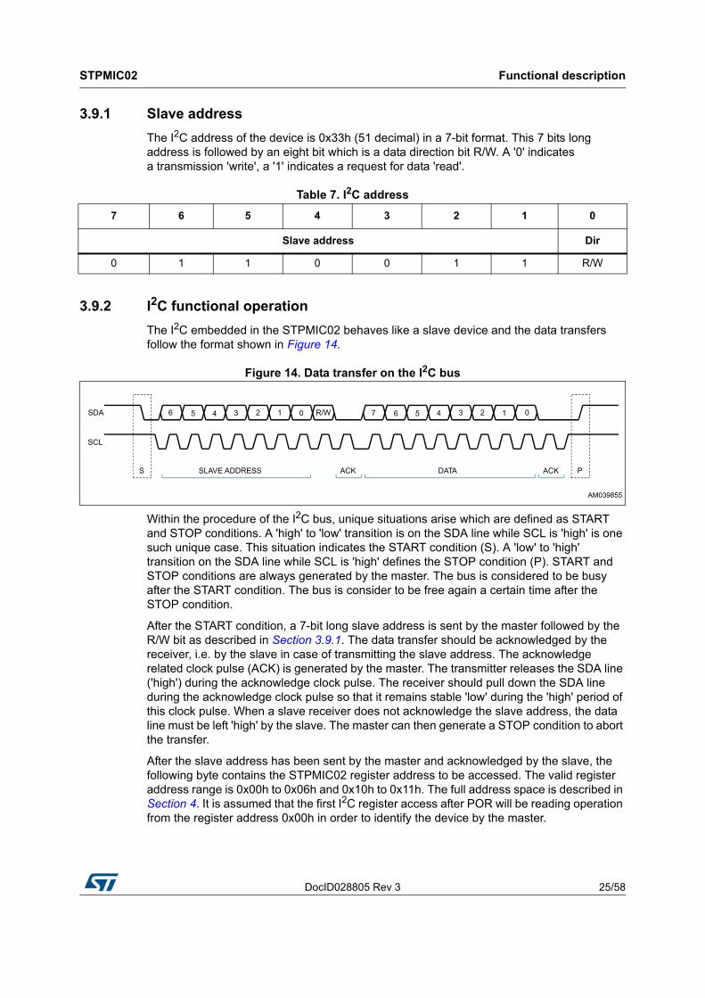
The I2C embedded in the STPMIC02 behaves like a slave device and the data transfers follow the format shown in Figure 14.
Figure 14. Data transfer on the I2C bus
Within the procedure of the I2C bus, unique situations arise which are defined as START and STOP conditions. A 'high' to 'low' transition is on the SDA line while SCL is 'high' is one such unique case. This situation indicates the START condition (S). A 'low' to 'high' transition on the SDA line while SCL is 'high' defines the STOP condition (P). START and STOP conditions are always generated by the master. The bus is considered to be busy after the START condition. The bus is consider to be free again a certain time after the STOP condition.
After the START condition, a 7-bit long slave address is sent by the master followed by the R/W bit as described in Section 3.9.1. The data transfer should be acknowledged by the receiver, i.e. by the slave in case of transmitting the slave address. The acknowledge related clock pulse (ACK) is generated by the master. The transmitter releases the SDA line ('high') during the acknowledge clock pulse. The receiver should pull down the SDA line during the acknowledge clock pulse so that it remains stable 'low' during the 'high' period of this clock pulse. When a slave receiver does not acknowledge the slave address, the data line must be left 'high' by the slave. The master can then generate a STOP condition to abort the transfer.
After the slave address has been sent by the master and acknowledged by the slave, the following byte contains the STPMIC02 register address to be accessed. The valid register address range is 0x00h to 0x06h and 0x10h to 0x11h. The full address space is described in Section 4. It is assumed that the first I2C register access after POR will be reading operation from the register address 0x00h in order to identify the device by the master.
Table 7. I2C address
7 6 5 4 3 2 1 0
Slave address Dir
0 1 1 0 0 1 1 R/W

Functional description STPMIC02
26/58 DocID028805 Rev 3
Figure 15. Setting register address operation
In case of a write cycle to a STPMIC02 register, the third byte is the actual data to be written to the register address specified in the second byte. A complete single byte write cycle would look like in Figure 16:
Figure 16. Single data byte write operation
However, if a master wishes to read data from the STPMIC02, it can generate a repeated START condition (SR) without first generating a STOP condition. In this case the slave address is transmitted twice, once for the register address write and once for the data read operation. The read transaction is ended by the master not acknowledging the data byte and generating the STOP condition.
Figure 17. Single data byte read operation
The STPMIC02 also supports multiple data read / write operations, automatically incrementing the register address after each data byte access. The multiple data write and multiple data read operations are shown in Figure 18.
Figure 18. Multiple data bytes write/read operation

DocID028805 Rev 3 27/58
STPMIC02 Register description and defaults
58
4 Register description and defaults
4.1 Serial port mapping
Table 8. Serial port mapping
Register
nameAddr. (dec.)
7 6 5 4 3 2 1 0
ID1 0 DEV1 DEV0 MID2 MID1 MID0 NID2 NID1 NID0
ID2 1 VID3 VID2 VID1 VID 0 FAB1 FAB0 Reserved <1:0>
0V9VSEL 2 - - 0V9Sel5 0V9Sel4 0V9Sel3 0V9Sel2 0V9Sel1 0V9Sel0
3V3VSEL 3 - - 0V9Key 3V3Sel4 3V3Sel3 3V3Sel2 3V3Sel1 3V3Sel0
CONTROL0 4 P3En ImonG VR33PWM VR09PWM Deglitch iMonEnVR09
MonDisVR09Dis
STATUS0 5 UV12 UV5 UV33 UV09 OT <1:0> EOTW12 EOTW5
STATUS1 6 OC12 OC5 OC33 OC09 P3state EOTW09 Reserved 1 Reserved 0
DeGlitch1 16 EFOV deglitch Reserved
DeGlitch2 17 - - - - EFOC deglitch

Register description and defaults STPMIC02
28/58 DocID028805 Rev 3
4.2 ID1 address = 0 (0x00h)
Table 9. Die ID1 register
7 6 5 4 3 2 1 0
DEV MID NID
R R R
0 1 - - - - - -
Table 10. Die ID1 bit description
Bit no. Bit name Description Meanings
7:6 DEV<1:0> Device 01 STPMIC02
5:3 MID<2:0> Major ID
001
010
011
100
101
110
111
1.x diffusion release
2.x
3.x
4.x
5.x
6.x
7.x
2:0 NID<2:0> Minor ID
000
001
010
011
100
101
110
111
x.0 metal release
x.1
x.2
x.3
x.4
x.5
x.6
x.7

DocID028805 Rev 3 29/58
STPMIC02 Register description and defaults
58
4.3 ID2 address = 1 (0x01h)
Table 11. Die ID2 register
7 6 5 4 3 2 1 0
VID FAB SID
R R R
0 0 0 0 OTP OTP 1 0
Table 12. Die ID2 bit description
Bit no. Bit name Description Meanings
7:4 VID <3:0> Variant ID - -
3:2 FAB <1:0> Fab.
00
01
10
11
ST Catania
1:0 Reserved <1:0> - - -
Register description and defaults STPMIC02
30/58 DocID028805 Rev 3
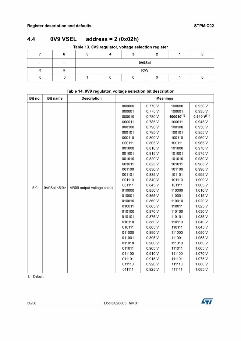
4.4 0V9 VSEL address = 2 (0x02h)
Table 13. 0V9 regulator, voltage selection register
7 6 5 4 3 2 1 0
- - 0V9Sel
R R R/W
0 0 1 0 0 0 1 0
Table 14. 0V9 regulator, voltage selection bit description
Bit no. Bit name Description Meanings
5:0 0V9Sel <5:0> VR09 output voltage select
000000
000001
000010
000011
000100
000101
000110
000111
001000
001001
001010
001011
001100
001101
001110
001111
010000
010001
010010
010011
010100
010101
010110
010111
011000
011001
011010
011011
011100
011101
011110
011111
0.770 V
0.775 V
0.780 V
0.785 V
0.790 V
0.795 V
0.800 V
0.805 V
0.810 V
0.815 V
0.820 V
0.825 V
0.830 V
0.835 V
0.840 V
0.845 V
0.850 V
0.855 V
0.860 V
0.865 V
0.870 V
0.875 V
0.880 V
0.885 V
0.890 V
0.895 V
0.900 V
0.905 V
0.910 V
0.915 V
0.920 V
0.925 V
100000
100001
100010(1)
100011
100100
100101
100110
100111
101000
101001
101010
101011
101100
101101
101110
101111
110000
110001
110010
110011
110100
110101
110110
110111
111000
111001
111010
111011
111100
111101
111110
111111
0.930 V
0.935 V
0.940 V(1)
0.945 V
0.950 V
0.955 V
0.960 V
0.965 V
0.970 V
0.975 V
0.980 V
0.985 V
0.990 V
0.995 V
1.000 V
1.005 V
1.010 V
1.015 V
1.020 V
1.025 V
1.030 V
1.035 V
1.040 V
1.045 V
1.050 V
1.055 V
1.060 V
1.065 V
1.070 V
1.075 V
1.080 V
1.085 V
1. Default.
DocID028805 Rev 3 31/58
STPMIC02 Register description and defaults
58
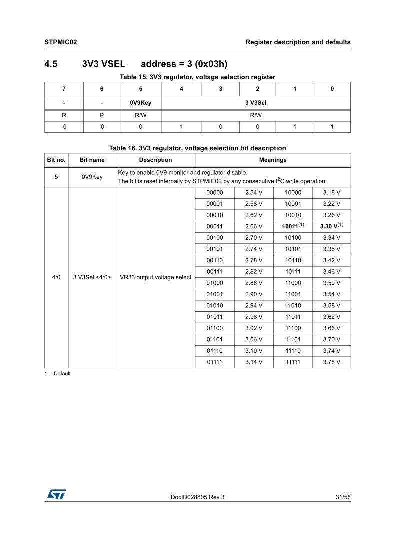
4.5 3V3 VSEL address = 3 (0x03h)Table 15. 3V3 regulator, voltage selection register
7 6 5 4 3 2 1 0
- - 0V9Key 3 V3Sel
R R R/W R/W
0 0 0 1 0 0 1 1
Table 16. 3V3 regulator, voltage selection bit description
Bit no. Bit name Description Meanings
5 0V9KeyKey to enable 0V9 monitor and regulator disable.
The bit is reset internally by STPMIC02 by any consecutive I2C write operation.
4:0 3 V3Sel <4:0> VR33 output voltage select
00000 2.54 V 10000 3.18 V
00001 2.58 V 10001 3.22 V
00010 2.62 V 10010 3.26 V
00011 2.66 V 10011(1)
1. Default.
3.30 V(1)
00100 2.70 V 10100 3.34 V
00101 2.74 V 10101 3.38 V
00110 2.78 V 10110 3.42 V
00111 2.82 V 10111 3.46 V
01000 2.86 V 11000 3.50 V
01001 2.90 V 11001 3.54 V
01010 2.94 V 11010 3.58 V
01011 2.98 V 11011 3.62 V
01100 3.02 V 11100 3.66 V
01101 3.06 V 11101 3.70 V
01110 3.10 V 11110 3.74 V
01111 3.14 V 11111 3.78 V

Register description and defaults STPMIC02
32/58 DocID028805 Rev 3
4.6 CONTROL0 address = 4 (0x04h)
Table 17. CONTROL0
7 6 5 4 3 2 1 0
P3En ImonG VR33PWM VR09PWM Deglitch iMonEn VR09MonDis VR09Dis
R/W R/W R/W R/W R/W R/W R/W R/W
0 0 0 0 0 0 0 0
Table 18. CONTROL0 register, bit description
Bit no. Bit name Description
7 P3EnP3 power disable feature enable.
The bit is reset internally by the STPMIC02 when undervoltage occurs on V5IN or V12IN supply voltage.
6 ImonG Current monitor gain
5 VR33PWM ForceVR33 to operate in PWM mode only.
4 VR09PWM ForceVR09 to operate in PWM mode only.
3 DeglitchDeglitch time selection for fault/POR detection (as specified in Section 7.4: VR09 on page 42).
2 iMonEn(1) E-fuse current monitor enable.
1 VR09MonDis
VR09 PG monitor disable.
The bit can be modified only if the bit 0V9Key has been set in previous write.
The bit is reset internally by the STPMIC02 when the VR09 performs transition (startup or output voltage change) or when the input pin VR09En is low.
0 VR09Dis
VR09 regulator disable (OFF).
The bit can be modified only if the bit 0V9Key has been set in previous write.
The bit is reset internally by the STPMIC02 when the input pin VR09En is low.
1. The iMonEn bit can be manually set or reset via I2C by the user. The iMonEn bit keeps its value during the overcurrent and/or overvoltage of any E-fuse The iMonEn bit is totally independent from any VR.
DocID028805 Rev 3 33/58
STPMIC02 Register description and defaults
58
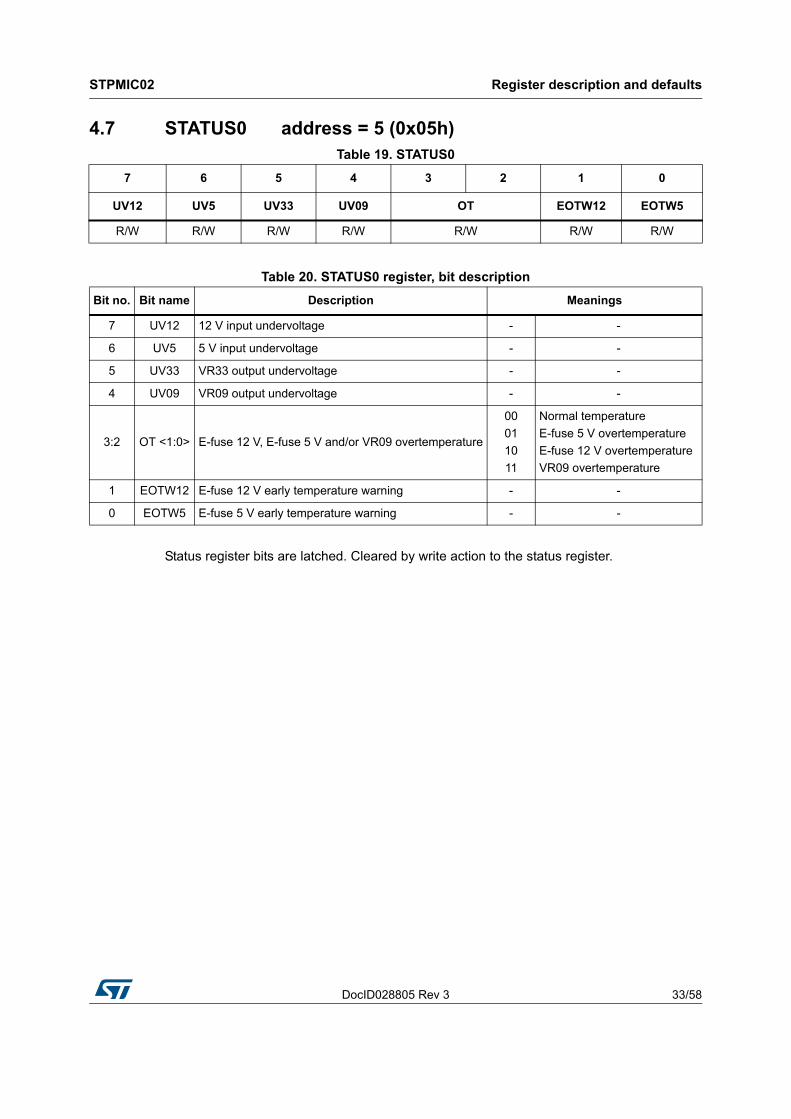
4.7 STATUS0 address = 5 (0x05h)
Status register bits are latched. Cleared by write action to the status register.
Table 19. STATUS0
7 6 5 4 3 2 1 0
UV12 UV5 UV33 UV09 OT EOTW12 EOTW5
R/W R/W R/W R/W R/W R/W R/W
Table 20. STATUS0 register, bit description
Bit no. Bit name Description Meanings
7 UV12 12 V input undervoltage - -
6 UV5 5 V input undervoltage - -
5 UV33 VR33 output undervoltage - -
4 UV09 VR09 output undervoltage - -
3:2 OT <1:0> E-fuse 12 V, E-fuse 5 V and/or VR09 overtemperature
00
01
10
11
Normal temperature
E-fuse 5 V overtemperature
E-fuse 12 V overtemperature
VR09 overtemperature
1 EOTW12 E-fuse 12 V early temperature warning - -
0 EOTW5 E-fuse 5 V early temperature warning - -

Register description and defaults STPMIC02
34/58 DocID028805 Rev 3
4.8 STATUS1 address = 6 (0x06h)
Status register bits are latched. Cleared by write action to the status register.
Table 21. STATUS1
7 6 5 4 3 2 1 0
OC12 OC5 OC33 OC09 P3state EOTW09 Reserved 1 Reserved 0
R/W R/W R/W R/W R/W R/W R/W R/W
Table 22. STATUS1 register, bit description
Bit no. Bit name Description
7 OC12 E-fuse 12 V overcurrent
6 OC5 E-fuse 5 V overcurrent
5 OC33 VR33 output overcurrent
4 OC09 VR09 output overcurrent
3 P3state Present P3 pin state
2 EOTW09 VR09 early temperature warning
1 Reserved 1 -
0 Reserved 0 -

DocID028805 Rev 3 35/58
STPMIC02 Register description and defaults
58
4.9 Deglitch1 address = 16 (0x10h)
4.10 Deglitch2 address = 17 (0x11h)
Table 23. E-Fuse overvoltage deglitch time register
7 6 5 4 3 2 1 0
EFOV deglitch Reserved
R/W R/W
1 0 1 0 0 0 0 0
Table 24. E-Fuse overvoltage deglitch time register, bit description
Bit no. Bit name Description Meanings
7:4 EFOV deglitch <3:0>E-fuse clamping deglitch time (falling edge only)
0000 5 µs 1000 40 µs
0001 6 µs 1001 48 µs
0010 7 µs 1010 56 µs
0011 8 µs 1011 64 µs
0100 9 µs 1100 72 µs
0101 10 µs 1101 80 µs
0110 11 µs 1110 88 µs
0111 12 µs 1111 96 µs
3:0 Reserved - - - - -
Table 25. E-Fuse overcurrent deglitch time register
7 6 5 4 3 2 1 0
- - - - EFOCdeglitch
R R R R R/W
0 0 0 0 0 0 1 1
Table 26. E-Fuse overcurrent deglitch time register, bit description
Bit no. Bit name Description Meanings
3:0 EFOC deglitch <3:0> E-fuse overcurrent deglitch time
0000
0001
0010
0011
0100
0101
0110
0111
2 µs
3 µs
4 µs
5 µs
6 µs
7 µs
8 µs
9 µs
1000
1001
1010
1011
1100
1101
1110
1111
16 µs
24 µs
32 µs
40 µs
48 µs
56 µs
64 µs
72 µs

Absolute maximum ratings STPMIC02
36/58 DocID028805 Rev 3
5 Absolute maximum ratings
The absolute maximum rating is the maximum stress that can be applied to a device without causing permanent damage. However, extended exposure to maximum ratings may affect long-term device reliability.
Table 27. Absolute maximum ratings
Parameter Limit Unit
12 V power input voltage (maximum 100 msec.) -0.3 to 25 (without external diode) V
5 V power input voltage (maximum 100 msec.) -0.3 to 15 (without external diode) V
12 V overcurrent protect 3.5 A
5 V overcurrent protect 3.5 A
V5OUTB, V5OUT -0.3 V to 7 V
V12OUT -0.3 V to 16.5 V
Operating junction temperature -10 to 150 °C
P3 input voltage -0.5 to 3.9 V
P3FW input voltage -0.5 to AVDD V
AVDD -0.5 to 2.5 V
SDA, SCL - I2C lines -0.3 V to 2.5 V
I5SNS, I12SNS -0.3 V to 7 V
PG09, PG33, EF5ON, VR09En, SINTn -0.3 V to 7 V
VR33FB -0.3 V to 5.7 V
VR09FB -0.3 V to 2.5 V
VR09SW, VR33SW -0.3 V to 7 V

DocID028805 Rev 3 37/58
STPMIC02 Typical operating conditions
58
6 Typical operating conditions
Unless otherwise indicated, performance specifications do not apply when the device is operated outside the recommended conditions.
Table 28. Typical operating conditions
Parameter Min. Typ. Max. Unit
12 V power input voltage 10.5 12 13.2 V
12 V power input current - - 2.5 A
5 V power input voltage 4.3 5.0 5.5 V
5 V power output voltage 2.5 - 5.5 V
5 V power input current - - 2.5 A
Serial I/F voltage 1.7 1.8 1.95 V
Operating ambient temperature -10 - 85 °C
Operating junction temperature -10 - 125 °C
P3 input voltage -0.3 3.3 3.6 V
P3FW input voltage -0.3 - AVDD V

Electrical characteristics STPMIC02
38/58 DocID028805 Rev 3
7 Electrical characteristics
Table 29. Device bias
Parameter Symbol Conditions Min. Typ. Max. Unit
Ibias - E-fuses ON, regulators OFF - 0.4 1.0 mA
Ibias - E-fuses OFF, regulators ON (not switching) through V5out - - 1.0 mA
Table 30. AVDD
Parameter Symbol Conditions Min. Typ. Max. Unit
Output voltage - - - 1.8 - V
PORn rising - - - 1.7 - V
PORn falling - - - 1.6 - V
External capacitor - - 0.5 1 1.5 µF
Table 31. P3 power disable
Parameter Symbol Conditions Min. Typ. Max. Unit
P3 low input voltage - Power enabled -500 - 700 mV
P3 high input voltage - Power disabled 2.1 - 3.6 V
P3 pull-down resistor - R pull-down 60 100 140 k
P3 input rising threshold - Rising 1.3 1.6 1.9 V
P3 input threshold hysteresis - Falling hysteresis 200 350 500 mV
P3FW low input voltage - P3 = w/NoFW enable -500 - 700 mV
P3FW high input voltage - P3 = w/FW enable 1.0 - AVDD V
P3FW high input current - P3FW pin input current - - 5.0 µA

DocID028805 Rev 3 39/58
STPMIC02 Electrical characteristics
58
7.1 E-fuse 12 V Table 32. E-fuse 12 V
Parameter Symbol Conditions Min. Typ. Max. Unit
On resistance RdsonTj = 25 °C - 45 - m
Tj = 125 °C - - 70 m
Off state leakage current Ioff - - - 1 µA
Continuous output current Iout - - 2.5 - A
Output clamp voltage Voclamp - 13.8 15 16.2 V
Input undervoltage lockout V12uv Falling 8.8 9.0 9.24 V
Undervoltage lockout hysteresis - Rsing hysteresis 600 700 800 mV
Current monitor output current gain
-Imon/IE-fuse , ImonG = 0 Iout > = 200 mA
237.5 250 262.5 µA/A
-Imon/IE-fuse , ImonG = 0100 mA < Iout < 200 mA
228 250 272 µA/A
- Imon/IE-fuse , ImonG = 1 475 500 525 µA/A
Current monitor voltage VI12snsMax. voltage with unaffected precision
- - V12out -1.5 V V
Startup current limit -Until V12out reaches its final value (either V12in or the output clamp voltage limit)
0.5 0.8 1.1 A
Short-circuit current limit - V12out < 7.5 V 0.5 0.8 1.1 A
Overload current limit -V12out > 7.5 V (see Section 3.1.1: E-fuse 12 V current limit on page 10)
3 3.5 4 A

Electrical characteristics STPMIC02
40/58 DocID028805 Rev 3
7.2 E-fuse 5 V
Table 33. E-fuse 5 V
Parameter Symbol Conditions Min. Typ. Max. Unit
Operating output voltage range
- - 2.5 - 5.5 V
On resistance RdsonTj = 25 °C - 45 - m
Tj = 125 °C - - 70 m
Off state leakage current Ioff - - - 1 µA
Continuous output current Iout - - 2.5 - A
Output clamp voltage Voclamp - 5.70 6.00 6.30 V
Input undervoltage lockout rising
Von E-fuse turn on voltage 4.25 4.35 4.45 V
Input undervoltage lockout falling
Voff E-fuse turn off voltage. 4.00 4.10 4.20 V
Output undervoltage comparator
VothThreshold to inform companion chip about power loss via EF5ON
- 4.4 - V
EF5ON falling delay - Both V5in and V5out UV - - 500 ns
Current monitor output current gain
-Imon/IE-fuse , ImonG = 0
Iuot > = 200 mA237.5 250 262.5 µA/A
-Imon/IE-fuse , ImonG = 0
100 mA < Iuot < 200 mA228 250 272 µA/A
- Imon/IE-fuse , ImonG = 1 475 500 525 µA/A
Current monitor voltage VI5sns Max. voltage with unaffected precision 0 - V5out -1.5 V V
Reverse current voltage E-fuse off
Vin-VoutPossible to program via OTP as follows: -30 mV, -40 mV, -60 mV and -90 mV
- -40 - mV
Reverse current voltage E-fuse on
- Vin-Vout - 0 - mV
Startup current limit -Until V5out reaches its final value (either V5in or the output clamp voltage limit)
0.5 0.8 1.1 A
Short-circuit current limit - V5out < 2.5 V 0.5 0.8 1.1 A
Overload current limit -V5out > 2.5 V (see Section 3.2.1: E-fuse 5 V current limit on page 13)
3 3.5 4 A
EF5on Logic0 output voltage
- Isink = 1 mA -300 - 400 mV
Iol - EF5on - Vol = 0.4 V - 11 - mA
EF5on max. output voltage - - - - V5outB V

DocID028805 Rev 3 41/58
STPMIC02 Electrical characteristics
58
7.3 VR33
Table 34. VR33
Parameter Symbol Conditions Min. Typ. Max. Unit
Operating input voltage range
- - 2.5 - 5.5 V
High-side FET on resistance HSrdson
- - 275 - m
At 125 °C, 5 Vout = 5 V, Io = 500 mA - 350 - m
At 125 °C, 5 Vout = 3 V, Io = 500 mA - 500 - m
Low-side FET on resistance LSrdson
- 425 - m
At 125 °C, 5 Vout = 5 V, Io = 500 mA - 640 - m
At 125 °C, 5 Vout = 3 V, Io = 500 mA - 900 - m
DC output current - - 0 - 300 mA
Peak inductor overcurrent cycle-by-cycle limit
Ipeak_max - 0.75 1 1.25 A
DC output voltage
- Code 00000 - 2540 - mV
- Code 10000 - 3180 - mV
- Code 11111 - 3780 - mV
Output voltage accuracy - - - ±1 ±3 %
DC output voltage step size - - - 40 - mV
VR33FB voltage range - - - V5outB V
Vout5B voltage to enable startup
- E-fuse 5 output voltage. - 4.0 - V
Soft-start slew rate SR - 5 6.25 7.5V/m
s
PG33 active voltage (falling) -PG level as function of output voltage setting
-9 -10 -11 %
PG33 deglitch filter- Deglitch = 0 - 200 - ns
- Deglitch = 1 - 1 - µs
PG33 Logic0 active output voltage
- Isink = 1 mA -300 - 400 mV
PG33 Logic1 in active output voltage delay
-PG33 output high delay from PG33 comparator output being good.
- 1 - ms
Total voltage output delta - 200 mA step in 100 ns. Including DC. -5 - 5 %
Switching frequency - - - - 6 MHz
Efficiency -At all operating conditions: V5out = 5.5 to 3 V, Iout = 150 mA, Rind = attempt (25 at RT) , Rpcb = attempt (10 m at RT)
80 90 - %
VR has 100% duty capability. - - - - - -
Output capacitor Co_vr33 All drift included 8.9 22 26.4 µF

Electrical characteristics STPMIC02
42/58 DocID028805 Rev 3
7.4 VR09
Output capacitor ESR Esr_vr33 At 4 MHz 1 - 30 m
Output inductor Lo_vr33 All drift included 0.56 1 1.2 µH
Output inductor resistance Rind_vr33 - - - 100 m
Table 34. VR33 (continued)
Parameter Symbol Conditions Min. Typ. Max. Unit
Table 35. VR09
Parameter Symbol Conditions Min. Typ. Max. Unit
Operating input voltage range - - 2.5 - 5.5 V
High-side FET on resistance HSrdson
- - 75 - m
At 125 ºC, Vgs = 5 V, Io = 500 mA - 90 - m
At 125 ºC, Vgs = 3 V, Io = 500 mA - 135 - m
Low-side FET on resistance LSrdson
- - 20 - m
At 125 ºC, Vgs = 5 V, Io = 500 mA - 30 - m
At 125 ºC, Vgs = 3 V, Io = 500 mA - 40 - m
DC/RMS output current - - 0 - 3.50 A
Pulse output current - Tpulse 500 µs - - 4.30 A
Peak inductor overcurrent cycle-by-cycle limit
Ipeak_max - 6.4 7.1 7.8 A
Overcurrent Toff time - - - 800 ns
DC output voltage
- Code 000000 - 770 - mV
- Code 100000 - 930 - mV
- Code 111111 - 1085 - mV
Output voltage accuracy - - - ±1 ±3 %
DC output voltage step size - - - 5 - mV
VR09En input voltage for VR09 turn-on
- VR09 turn on voltage 1.0 - 3.65 V
VR09En input voltage for VR09 turn-off
- VR09 turn off voltage -0.3 - 0.4 V
VR09En input voltage hysteresis for VR09 turn off.
- VR09 turn-off hysteresis 100 200 - mV
VR09En input bias - - - - 1 µA
Soft-start slew rate SR - 1 1.5 2 V/ms
PG09 activation voltage -PG voltage as percentage of output voltage setting
-9 -10 -11 %
PG09 deglitch filter -Deglitch = 0 - 200 - ns
Deglitch = 1 - 1 - µs

DocID028805 Rev 3 43/58
STPMIC02 Electrical characteristics
58
7.5 Temperature monitor
PG09 Logic0 active output voltage - Isink = 1 mA -300 - 400 mV
PG09 Logic1 in active output voltage delay
-PG09 output high delay from PG09 comparator output being good.
- 1 - ms
Total output voltage delta - 1A75 step in 100 ns -5 5 %
Switching frequency - - - 2 - MHz
Efficiency -
V5out = 5, Iout = 1A5,
Rind = attempt (25 at RT),
Rpcb = attempt (10 at RT)
- 79 - %
Output capacitor Co_vr09All drift included
2 x 47 µF in //28 44 113 µF
Output capacitor ESR Esr_vr09 At 2 MHz for each of the 47 µF cap 1 - 20 m
Output inductor Lo_vr09 All drift included 0.26 0.47 0.57 µH
Output inductor resistance Rind_vr09 - - 30 50 m
Table 35. VR09 (continued)
Parameter Symbol Conditions Min. Typ. Max. Unit
Table 36. Temperature monitor
Parameter Symbol Conditions Min. Typ. Max. Unit
Early overtemperature warning EOTW - 130 145 160 °C
Overtemperature threshold OTth - 150 165 180 °C
Overtemperature hysteresis OThys - - 50 - °C
Temperature warning to shutdown tracking Tdelta OTth- EOTW 15 20 25 °C

Electrical characteristics STPMIC02
44/58 DocID028805 Rev 3
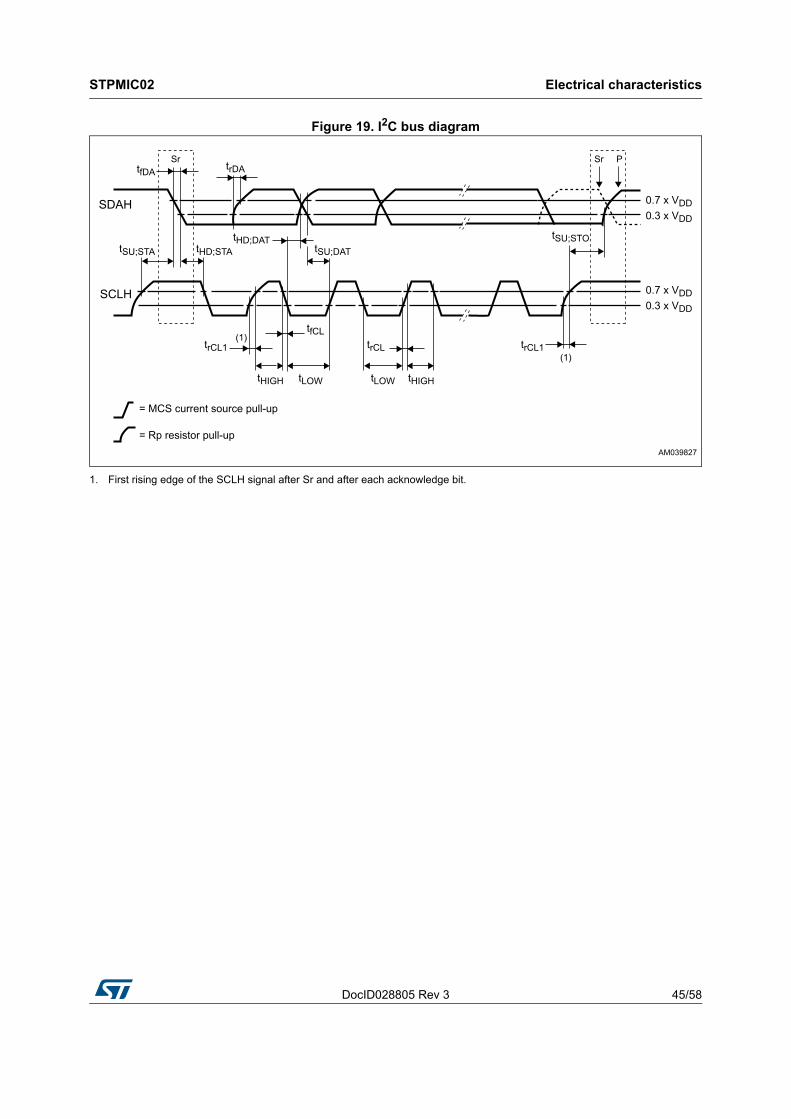
7.6 I2C bus
Table 37. I2C(1)
Parameter Symbol Conditions Min. Typ. Max. Unit
Vol-SINTn - Vol = 7 mA - - 0.4 V
Iol-SINTn - Vol = 0v4 7 12 - mA
VDD for I2C interface - - 1.7 1.8 1.95 V
Vil - Logic0 input voltage -0.5 - 0.3 VDD V
Vih - Logic1 input voltage 0.7 VDD - VDD +0.5 V
Vihyst - Input hysteresis 0.1 VDD - - V
Iin - Input current, Vi = 0.1 VDD to 0.9 V -10 - 10 µA
Vol-SDA - Logic0 output voltage, Isink = 2 mA 0 - 0.2 VDD V
Iol-SDA - Vol = 0.4 V 6 8 - mA
Ron-SDA - Vol = 0.4 V - 50 -
Input voltage deglitch - - 0 - 10 ns
SCL clock frequency - - 0.1 - 3.4 MHz
tsu, start/stop - Setup time 160 - - ns
thold, start/stop - Hold time 160 - - ns
tlow, SCL - Low pulse time 160 - - ns
thi, SCL - High pulse time 60 - - ns
tsu, SDA - Data setup time 10 - - ns
thold, SDA - Data hold time 0 - 70 ns
trise, tfall, SCL receiver - Clock rise/fall time 20 - 1000 ns
trise, tfall, SDA receiver - Data rise/fall time 20 - 1000 ns
tfall, SDA transmitter - (2) 20 - 40 ns
1. The I2C signals must be compliant to the characteristic standard I2C bus, the device is compatible with the mode “Normal”, “Fast”, “Fast Plus” and “High Speed”.
2. This need to be achieved with the help of the pull-up resistor (and if needed extra cap) taking in consideration the board and the load (C and R) connected to the SDA pin.
DocID028805 Rev 3 45/58
STPMIC02 Electrical characteristics
58
Figure 19. I2C bus diagram
1. First rising edge of the SCLH signal after Sr and after each acknowledge bit.

Application details STPMIC02
46/58 DocID028805 Rev 3
8 Application details
8.1 Regulators sequencing
Figure 20. Regulators sequencing

DocID028805 Rev 3 47/58
STPMIC02 Application details
58
A typical power-on sequence for the system is as follows:
1. The V5IN and/or V12IN goes above the required operating voltage to start the STPMIC02.
2. If the V5IN is above the UV5 threshold, the E-fuse 5 V starts ramping its output.
3. If the V12IN is above the UV12 threshold, the E-fuse 12 V starts ramping its output. Since the E-fuses are independent from each other, it can happen that both E-fuse 5 V and E-fuse 12 V are ramping up at the same time.
4. Upon the V5OUTB crossing the regulator minimum operating voltage for turn ON, the VR33 starts up.
5. After the VR33 output crosses its PG detection threshold, the PG33 signal goes to Logic1 1 ms after the last time that the VR33 is above its target have stabilized.
6. The VR09 starts up after the VR09EN pin is at the Logic1 state.
7. After the VR09 output crosses its PG detection threshold, the PG09 signal goes to Logic1 1 ms after the last time that VR09 is above its target have stabilized.
8. If the V5IN or V12IN input fails, its respective E-fuse 5 V / E-fuse 12 V is open.
9. If both V5IN and V12IN inputs fail, both E-fuse 5 V / E-fuse 12 V are open and the STPMIC02 continues operating from the V5OUTB.
8.2 Disabling VR33
The VR33 is an always-on regulator. As soon as the V5OUTB is present and above the UV threshold, the VR33 is enabled. The VR33 does not have a corresponding bit in the register map that would allow to switch off (disable) the regulator.
In case the VR33 is not used in an application, it has to be configured in such a way that prevents the VR33 from switching in order to save switching losses and to have the regulator in a defined state. In particular, the user has to:
Pull the VR33FB pin to the V5OUTB with resistance lower than 1 k (can also be a short).
Force the VR33PWM bit in the CONTROL0 register to Logic1 before enabling the VR09.
In this state, the STPMIC02 internal low-side power device of the VR33 is turned on, pulling the VR33SW node to ground. Since the state of the VR33SW pin is defined by the STPMIC02 itself in this configuration, there is no need to populate the L and C components related to the VR33 on the PCB.
Figure 21. Hardware 3.3 V regulator disable

Application details STPMIC02
48/58 DocID028805 Rev 3
Table 38. Fault function
Signals (which are latched)
Type of fault PG09 PG33SINTn
pinE-fuse 5 V
E-fuse 12 V
0.94 V regulator
3.3 V regulator
Status set
Vin12 undervoltage H H H L - Open Enable Enable UV12
V5in undervoltage H H H L Open - Enable Enable UV5
Vout12 overcurrent(1) H H H L ClosedEnable(Iout12 limit)
Enable Enable OC12
Vout5 overcurrent(1) H H H LEnable
(Iout5 limit)Closed Enable Enable OC5
0.9 V reg. output UV (-10%)
H L H H L Closed ClosedEnable
(recovery)Enable UV09
3.3 V reg. output UV (-10%)
H H L H L Closed Closed EnableEnable
(recovery)UV33
0.9 V overcurrent H H H L Closed ClosedEnable
(Iout limit)Enable OC09
3.3 V overcurrent H H H L Closed Closed EnableEnable
(Iout limit)OC33
12 V early overtemp. warning
H H H L Closed Closed Enable Enable EOTW12
5 V early overtemp. warning
H H H L Closed Closed Enable Enable EOTW5
0.9 V early overtemp. warning
H H H L Closed Closed Enable Enable EOTW09
5 V overtemperature H H H L Open Closed Enable Enable OT5
12 V overtemperature H H H L Closed Open Enable Enable OT12
0.9 V overtemperature H H H L Closed Closed Enable Enable OT5 and 12
V5outB UV 2.5 V for regulator operation (cannot maintain regulator performance)
L L H - - Disable Disable -
P3 pin Logic1 (feature enabled)
- - H L Open Open - -P3state
match pin
1. An overcurrent during the start-up is not a fault, it signals ramp-up in progress, the load should be less than the startup current limit.

DocID028805 Rev 3 49/58
STPMIC02 Package information
58
9 Package information
In order to meet environmental requirements, ST offers these devices in different grades of ECOPACK® packages, depending on their level of environmental compliance. ECOPACK® specifications, grade definitions and product status are available at: www.st.com. ECOPACK® is an ST trademark.
9.1 VQFN 24-pin 3.5 mm x 4. 5 mm x 1.0 mm, 0.5 mm pitch with EPAD type package information
Figure 22. VQFN 24-pin 3.5 mm x 4. 5 mm x 1.0 mm, 0.5 mm pitch with EPAD type package outline

Package information STPMIC02
50/58 DocID028805 Rev 3
Table 39. VQFN 24-pin 3.5 mm x 4. 5 mm x 1.0 mm, 0.5 mm pitch with EPAD type package dimensions
SymbolDimensions
Min. Nom. Max.
A 0.80 0.85 0.90
A1 - 0.05 -
b 0.20 0.25 0.30
D 3.45 3.50 3.55
D2 Variation
D3 Variation
D4 Variation
E 4.45 4.50 4.55
E2 - Variation -
E3 - Variation -
E4 - Variation -
e 0.50 BSC
L 0.35 0.40 0.45
k 0.40 - -
N - 24 -

DocID028805 Rev 3 51/58
STPMIC02 Recommended external components
58
10 Recommended external components
Table 40. Recommended external components
From To Description Value Unit
VR09FB GND Output capacitor 2 x 47 or 2 x 22 or 1 x 47 µF
VR09SW VR09FB Inductor 0.47 µH
VR33FB GND Output capacitor 22 µF
VR33SW VR33FB Inductor 1 µH
AVDD GND Capacitor 1 µF
System supply V5in Lead inductance <1 µH
V5in GND Capacitor 1 µF
V5out GND Capacitor>10 (STPMIC02)
>47 or >2 x 22 (application) µF
System supply V12in Lead inductance <1 µH
V12in GND Capacitor 1 µF
V12out GND Capacitor >10 µF

PCB design rules guideline STPMIC02
52/58 DocID028805 Rev 3
11 PCB design rules guideline
11.1 Basic principles
A step-down converter reduces an incoming voltage to a lower output voltage. A switching element, typically a bipolar or a MOSFET is switched on and off. When the switch is on, the input supply charges the inductor and capacitor and delivers power to the load. During this time, the magnitude of the inductor current ramps up as it flows through the Loop 1.
When the MOSFET turns off, the input is disconnected from the output, and the inductor and output capacitor support the load. The magnitude of the inductor current ramps down as it flows through the recirculating element, following the direction indicated in the Loop 2. The recirculating element can be a diode, but recently a more efficient synchronous rectification system is used where a second switching element takes over the function of the diode.
Figure 23. Current loops

DocID028805 Rev 3 53/58
STPMIC02 PCB design rules guideline
58
11.2 Layout rules
A multilayer board is preferred using the top layer to contain all power routing for the devices, and the inner layer 1 as a ground return plane.
Figure 24. Layer stack
11.2.1 Supplies
An incoming supply per switcher should be adequately buffered using an input capacitor. Refer to the device specification for suggested values. This capacitor needs to be placed as close as possible to the VIN pin to minimize the loop area.
11.2.2 Switch node
The switch node is the pin feeding the inductor. Keep the switch node as short as possible to avoid power losses. Do not make it wider than necessary to avoid capacitive loading of the switch node.
11.2.3 Feedback node
The feedback node is a high impedance input and thus sensitive to noise and current injection through the capacitive and magnetic coupling. Keep the feedback lines away from large switching surfaces or magnetic fields. Remember that magnetic fields are not stopped by copper!
Feedback components should be connected to a clean return pathway and never share return paths with the main switching elements.
11.2.4 Output capacitors
Multiple output capacitors are preferred over a single one. Each capacitor should have its own return via.

PCB design rules guideline STPMIC02
54/58 DocID028805 Rev 3
11.2.5 PCB layout recommendation
Figure 25. All layers
Figure 26. All layers (through view)

DocID028805 Rev 3 55/58
STPMIC02 PCB design rules guideline
58
Figure 27. Top layer
Figure 28. Bottom layer

PCB design rules guideline STPMIC02
56/58 DocID028805 Rev 3
11.3 General rules
Do not share vias. Every component connecting to the power or reference plane needs its own via. For large currents multiple vias are to be preferred.
Vias shall be placed as close to the component pin as possible.
Feedback nodes are sensitive. Keep them away from magnetic fields and nodes that may capacitive couple energy into them.
11.4 Thermal aspects
The device package uses the center pad as a thermal conduit. This pad should be connected to an adequate spread of copper. When following the suggested layer stack the internal ground plane may be sufficient. If lots of other heat generating components are close by it may be necessary to create an exposed copper area on the backside of the board. The pad should be connected using multiple vias.

DocID028805 Rev 3 57/58
STPMIC02 Evaluation tool
58
12 Evaluation tool
An evaluation tool is available upon request. Please contact your local ST sales representative for availability.
13 Revision history
Table 41. Document revision history
Date Revision Changes
22-Dec-2015 1 Initial release.
01-Feb-2016 2Updated document status to Datasheet - production data.
Minor modifications throughout document.
03-Mar-2016 3Updated Section 3.9 on page 24 (added Section 3.9.1 on page 25 and Section 3.9.2 on page 25).
Minor modifications throughout document.

STPMIC02
58/58 DocID028805 Rev 3
IMPORTANT NOTICE – PLEASE READ CAREFULLY
STMicroelectronics NV and its subsidiaries (“ST”) reserve the right to make changes, corrections, enhancements, modifications, and improvements to ST products and/or to this document at any time without notice. Purchasers should obtain the latest relevant information on ST products before placing orders. ST products are sold pursuant to ST’s terms and conditions of sale in place at the time of order acknowledgement.
Purchasers are solely responsible for the choice, selection, and use of ST products and ST assumes no liability for application assistance or the design of Purchasers’ products.
No license, express or implied, to any intellectual property right is granted by ST herein.
Resale of ST products with provisions different from the information set forth herein shall void any warranty granted by ST for such product.
ST and the ST logo are trademarks of ST. All other product or service names are the property of their respective owners.
Information in this document supersedes and replaces information previously supplied in any prior versions of this document.
© 2016 STMicroelectronics – All rights reserved