power and delay performance of graphene based circuits ...06)/z-g050602660277.pdf · power and...
TRANSCRIPT
American Journal of Engineering Research (AJER) 2016
American Journal of Engineering Research (AJER)
e-ISSN: 2320-0847 p-ISSN : 2320-0936
Volume-5, Issue-6, pp-266-277
www.ajer.org Research Paper Open Access
w w w . a j e r . o r g
Page 266
Power and Delay Performance of Graphene-based Circuits
Including Edge Roughness Effects
Yaser M. Banadaki1, Safura Sharifi
2,3, Walter O. Craig III
1, Hsuan-Chao Hou
3
1(College of Science and Engineering, Southern University and A&M College, Baton Rouge, LA 70813, U.S.A.)
2(College of Science, Louisiana State University, Baton Rouge, LA 70803, U.S.A.)
3(Department of Electrical and Computer Engineering, Louisiana State University, Baton Rouge, LA 70803,
U.S.A.)
ABSTRACT : In this paper, we evaluate the effect of edge roughness on power and delay performance of
graphene nanoribbon field effect transistors (GNRFETs) in all-graphene architecture. The equivalent circuit
model of the multi-channel GNR FET is developed by incorporating the thermionic emission and band-to-band-
tunneling (BTBT) of carriers, as well as the effects of line-edge roughness on the carrier transport in graphene
nanoribbon. Our results show that the power and delay of ideal-edge GNRFET outperform Si-CMOS
technology at scaled supply voltages. However, edge roughness significantly degrades the performance of
GNRFET circuits, such that its 320 times smaller energy-delay product at VDD = 0.4V increases to %10 and
%40 of Si-CMOS for the roughness amplitude ( GNRW W ) of 0.04 and 0.1, respectively.
Keywords -graphene nanoribbon, edge roughness, energy-delay product, scaled supply voltages.
I. INTRODUCTION
The driving engine for the exponential growth of digital information processing systems is scaling
down the transistor dimensions. For decades, this has enhanced the device performance, leading to denser chips
with more functionality, a lower price per chip, faster switching and lower power consumption. However,
International Technology Roadmap for Semiconductors (ITRS) [1] has specified critical challenges to sustain
the historical scaling of silicon technology. Toward or beyond the end of this roadmap period, when the current
silicon-CMOS technology will likely become ineffective and prohibitively costly, the genesis of new materials
will be needed to continue improvements in device performance. Graphene [2]and carbon nanotube (CNT) [3]
are the two carbon allotropes, which have become prominent contenders to substitute silicon in post-CMOS
technology. Graphene, one atomic layer of carbon sheet, may outperform state-of-the-art silicon for many
applications due to its exceptional electronic properties. The carrier transport in graphene is similar to the
transport of massless particles since 2D electron gas in graphene provides both high carrier velocity and high
carrier concentration, resulting in large carrier mobility and, consequently, faster switching capability [4].
However, graphene is a semimetal with a zero bandgap while it is basic requirement for digital integrated
circuits. The quantum confinement of graphene sheet in the form of one-dimensional strips known as graphene
nanoribbon (GNR) provides the energy gap of several hundred meV required for FET operation in digital
applications [5].
In theory, the GNRs can be produced by patterning planar 2D graphene using standard fabrication
methods with much more controllability than their counterparts, carbon nanotubes. However, the state-of-the-art
patterning technique is far from achieving atomic-scale precision and GNRs with perfect smooth edges cannot
be fabricated. Thus, the edge roughness may play an important role in the production of narrow GNRs, such that
it shortens the mean free path (MFP) of electrons and consequently eliminates the attractive electron transport
properties of graphene [6]. As such, the efforts of most current research are to fabricate smooth-edge GNRs to
preserve the superior electronic quality of graphene. Yang and Murali[7] experimentally observed the linewidth-
dependent mobility of electrons in GNR, showing that electron mobility degrades by decreasing the GNR width
below 60 nm. Edge roughness is increased by scaling down the minimum feature size due to increase in
manufacturing variants of lithography and dry etching processes. GNR with precisely defined width can be
produced by the scalable bottom-up approach beyond the precision limit of modern lithographic approach [8].
However, both GNR-based devices and interconnects can be concurrently patterned using lithography method,
resulting in the advantages of bandgap engineering in all-graphene architecture [9].
As the fabrication technology of graphene nanoribbon is still in an early stage, the performance
American Journal of Engineering Research (AJER) 2016
w w w . a j e r . o r g
Page 267
evaluation of futuristic graphene-based circuits requires a GNR FET model with some parameters attributed to
the strength of edge roughness. Line-edge roughness may play an important role in the performance degradation
of a GNR FET by enhancing the edge scattering and generating edge states in its opened bandgap [10].
Although, the ideal smooth-edge GNR FETs give an estimation of the upper bound performance, modeling edge
roughness is vitally important to examine the effect of process variation on the performance of practical all-
graphene circuits. The edge roughness is mostly investigated using numerical methods due to its statistical
nature, which cannot be effectively implemented in circuit simulators. The results of device-level quantum
transport simulations of GNRFET can be introduced using lookup table techniques for circuit simulations [11].
However, the intensive numerical simulations need to be repeated with a single change in a design parameter to
rebuild the model accordingly. This makes it inappropriate for evaluating the optimized design parameters of
GNR FET circuits.
In this work, we investigate the effect of edge roughness on the power and delay performance of
GNRFETs by developing an analytical model of multi-GNR channel FET in SPICE. The organization of this
paper is as follows: In Section 2, we describe the advantage and challenge of all-graphene circuits, as well as the
structure and parameters of a GNR FET in this structure. Section 3 presents the equivalent circuit model of the
GNR FET by incorporating the thermionic emission and band-to-band-tunneling (BTBT) of carriers, as well as
the effects of line-edge roughness on the carrier transport in graphene nanoribbon [10]. In Sections 4, we
investigate the delay, power, and energy-delay product of GNRFETs for various edge roughness amplitudes and
supply voltages. The discussion is presented by comparing with 16-nm node Si-CMOS designed by 5-stage
fanout-of-4 buffer chain. Finally, the last section draws summarizing conclusions.
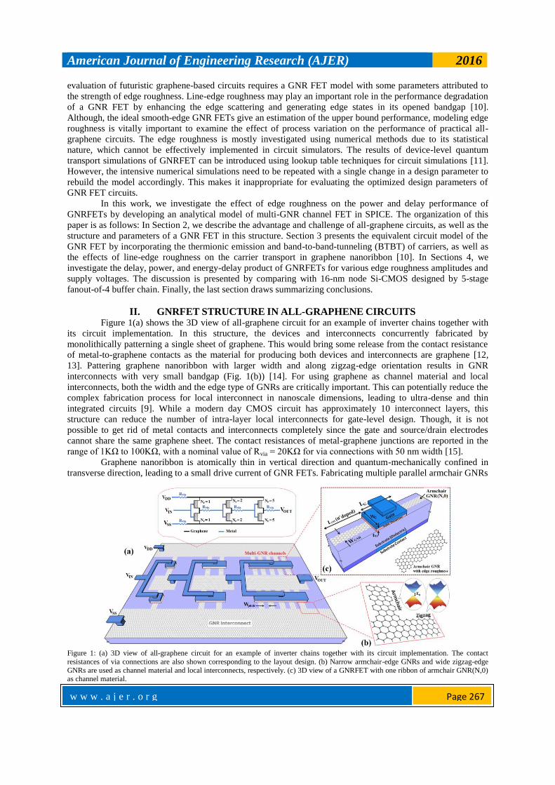
II. GNRFET STRUCTURE IN ALL-GRAPHENE CIRCUITS Figure 1(a) shows the 3D view of all-graphene circuit for an example of inverter chains together with
its circuit implementation. In this structure, the devices and interconnects concurrently fabricated by
monolithically patterning a single sheet of graphene. This would bring some release from the contact resistance
of metal-to-graphene contacts as the material for producing both devices and interconnects are graphene [12,
13]. Pattering graphene nanoribbon with larger width and along zigzag-edge orientation results in GNR
interconnects with very small bandgap (Fig. 1(b)) [14]. For using graphene as channel material and local
interconnects, both the width and the edge type of GNRs are critically important. This can potentially reduce the
complex fabrication process for local interconnect in nanoscale dimensions, leading to ultra-dense and thin
integrated circuits [9]. While a modern day CMOS circuit has approximately 10 interconnect layers, this
structure can reduce the number of intra-layer local interconnects for gate-level design. Though, it is not
possible to get rid of metal contacts and interconnects completely since the gate and source/drain electrodes
cannot share the same graphene sheet. The contact resistances of metal-graphene junctions are reported in the
range of 1KΩ to 100KΩ, with a nominal value of Rvia = 20KΩ for via connections with 50 nm width [15].
Graphene nanoribbon is atomically thin in vertical direction and quantum-mechanically confined in
transverse direction, leading to a small drive current of GNR FETs. Fabricating multiple parallel armchair GNRs
Figure 1: (a) 3D view of all-graphene circuit for an example of inverter chains together with its circuit implementation. The contact
resistances of via connections are also shown corresponding to the layout design. (b) Narrow armchair-edge GNRs and wide zigzag-edge
GNRs are used as channel material and local interconnects, respectively. (c) 3D view of a GNRFET with one ribbon of armchair GNR(N,0) as channel material.

American Journal of Engineering Research (AJER) 2016
w w w . a j e r . o r g
Page 268
in an array connected to the same wide zigzag GNRs can increase the drive current, leading to better switching
attribute for high-performance applications [16]. As such, the number of GNR channels (Nr) in a GNR FET can
correspond to integer increment of W/L in conventional CMOS. As the bandgap of GNRs can be inversely
changed by the GNR width (WGNR), it provides another degree of freedom for designer to use the bandgap
engineering in GNRFET circuits [17]. The length of local GNR interconnects between transistors within logic
gates are much shorter than the mean free path of graphene. In addition, the GNR interconnects are wide enough
to maintain the condition of very small bandgap. Therefore, the effects of edge roughness on interconnects can
be neglected. Also, the resistance and capacitance of local GNR interconnects can be assumed negligible in
first-order models [11].
The multi-channel GNR FET can be interpreted as several parallel individual GNR FETs as shown in
Fig. 1(c). In a MOSFET-like structure, the intrinsic GNR channel (LCH) has the same length underneath as the
gate contact (LG). However, the gate width (WG) is extended equally from each side of the GNR channel to
enhance the electrostatic control of the gate voltage over the channel potential barrier. The width of the intrinsic
GNR is GNR ccW =(N+1) 3a /2 , where cca is the carbon-carbon bonding length and N is the number of dimer
lines for the armchair GNR (N,0). The symmetric regions between the gate and contacts (LRES) are doped with
the n-type dopants concentration of dopf per carbon atom as the source and drain reservoirs. The insulator layer
between metallic gate and graphene nanoribbon is assumed aluminum nitride (AlN) with a relative dielectric
permittivity of κ = 9. The thin AlN dielectric layers can be deposited with good reproducibility and uniformity
[18], which results in small phonon scattering on epitaxial graphene and near ballistic carrier transport in a short
channel GNR FET [19].
III. MODEL EQUATIONS The multi-channel GNRFET consists of several parallel graphene nanoribbons and can be implemented
by sharing the gate, source, drain and substrate electrodes among all independent ribbons, together with two
parasitic capacitances (CGD and CGS) for fringing fields between the gate and the reservoirs as shown in Fig.
2(a). Figure 2(b) shows the energy band diagram and the corresponding components in the equivalent circuit
model of a GNR FET with individual GNR channel. The capacitors (CG,CH, CS,CH, CB,CH, and CD,CH) model the
electrostatic coupling of the channel to the potentials at gate, source, substrate, and drain electrodes,
respectively. Two current sources (IT and IBTBT) model the carrier transport associated with the thermal emission
of carriers over the channel potential barriers and band-to-band-tunneling (BTBT) from drain to channel
regions. A voltage-controlled voltage source (VCH) in the model accounts for the charging and discharging the
GNR channel.
The minimum energy ( bE ) and effective mass (*
bm ) of subbands for different armchair GNRs need to
be obtained using nearest neighbor tight-binding (NNTB) calculation based on orthogonal pz orbitals as basic
functions. The nearest neighbor hopping energy for the atoms not located at the edge is t = −2.7 eV, while it is
assumed 1.12t for the pairs of carbon atoms along the edges of the graphene nanoribbon. This accounts for
theedge bond relaxation due to the lattice termination and occupation of hydrogen atoms at the edges [20]. The
minimum energy and effective mass of subbands for different armchair GNRs are used in calculating the charge
density and current transport equations.
In n-type GNR FETs, the hole concentration in the channel is suppressed due to the n-doped drain and
source reservoirs and the electron concentration ( bn ) of bth subband can be obtained as follows:
0
( ) ( )b bn f E D E dE
(1)
*2( )( )
( 2 )
b b
b
b b
E E mD E
E E E E
(2)
where is the reduced Planck constant, ( )bD E is density of states of GNR and ( )f E is the Fermi-Dirac
distribution function. The electron concentration in GNRs can be evaluated considering the relative location of
Fermi levels at the terminals to conduction band energy ( ,
b b
FC F i CE E E ). Equation (3) provides a smooth
transition between two approximations: (1) exponential carrier concentration (exp
bn ) when the Fermi level is near
the conduction band (high DOS, 0FCE ); and (2) step carrier concentration (step
bn ) when the Fermi level is 3kT

American Journal of Engineering Research (AJER) 2016
w w w . a j e r . o r g
Page 269
away from the subband energy ( 3kTFCE ) [21].
exp( ) ( ) (1 ) ( )b step b
b FC b FC b FCn E w n E w n E (3)
* 3
exp1 2
( ) exp( / )2
b b
b FC FC
b
m En E E
E
(4)
*( ) (2 / ) max(( ( 2 ) ),0)step
b FC b FC FC b bn E m E E E E (5)
where 1/ [1 exp(3( kT) / kT)]FCw E is the relative weight of the two approximations and
3kT / ln ( ) (1 exp((3kT ) / kT))FC FCf E E . Thus, the total electron density in the GNR channel can be
obtained by summation over the carrier density of subbands as follows:
[ ( ( )) ( ( )) ) ]2
n b bCHGNR b FS C b FD C
b
q LQ n E E E n E E E (6)
where q is an electron charge and b
C b chE E is the conduction band energy. FS F SE E qV and
FD F DE E qV are the Fermi levels corresponding to the voltages at source and drain electrodes, respectively.
The induced charge by capacitance network can be calculated as follows [22]:
, ,
,
( )n
CAP i CH i FB i ch
i G B
Q C V V q
(7)
where VFB is the flat-band voltage due to the work function difference between metal and graphene and ch is
the channel surface potential. ,G CHC and ,B CHC are the geometrical capacitances, which model the electrostatic
coupling between the GNR channel and the gate and substrate electrodes, respectively. As the gate width is
larger than the GNR width and the oxide thickness, these two capacitances and parasitic capacitances between
the gate and the reservoirs ( ,G DC and ,G SC ) can be modeled by the analytical equation of micro-strip lines [23]
as follows: 11
,
0.55 10[ ]
ln[5.98 (0.8 )]i CH G
ox GNR GNR
C L pFt W t
(8-1)
2(1.9 25 100) [ ]GD GS G ox oxC C W t t pF (8-2)
where 0GNRt is the GNR thickness, oxt is the dielectric thickness, and 1(1 1.5 )ox Gt W is a correction
term for a case when the gate width is not much larger than the oxide thickness [24]. The transient intrinsic
capacitors ( ,S CHC and ,D CHC ) can be computed by introducing the derivatives of the channel charge with respect
to drain and source voltages. These modeled by two voltage-controlled capacitors in SPICE.
It is crucially important to evaluate the channel surface potential in GNR FET due to the small density
of states (DOS) of GNR channel. This can be found using the charge conservation equations by equating the
induced charge by the capacitances networks (QCAP) and the charge capacity of the GNR channel (QGNR). These
charges are implemented as the values of two voltage-controlled current sources in series [25]. This forces two
charges to be equal in magnitude, resulting in the automatic calculation of the channel voltage (VCH) and the
corresponding channel surface potential ( ch ) in SPICE. Given the surface potential ( ch ), both the DC and
AC behaviors of GNR FETs can be incorporated in the current calculation associated with thermionic current
(IT) for electrons with energies above the channel potential barrier and band-to-band tunneling, (IBTBT) between
hole states in the drain and electron states in the channel. The direct tunneling from source reservoir to drain
region can be neglected for the channel length larger than 10 nm. The thermionic current can be computed using
the Landauer-Buttiker formalism [26] as follows:
0
2( )[ ( ( )) ( ( )) ]b b
T FS C FD C
b
qI T E f E E E f E E E dE
h
(9)
where h is Planck constant. The integral in the above expression can be evaluated analytically with the Fermi-
Dirac integral of order 0, which results in the current at the ballistic limits as follows:
2[ln(1 exp(( ) / )) ln(1 exp(( ) / ))]b b
T B FS C FD C
b
qI k T E E kT E E kT
h (10)
American Journal of Engineering Research (AJER) 2016
w w w . a j e r . o r g
Page 270
In subthreshold region, the band-to-band-tunneling (BTBT) can be comparable to the thermionic
emission of carriers for small bandgap GNR FETs. Assuming ballistic transport for the tunneling process, the
BTBT current can be approximated as follows [25]:
, ,
,
1 exp(( ) / ) max( 2 ,0)2[ ln( ) ]
1 exp(( ) / ) 2
CH D b F B CH D b
BTBT B BTBT
b b F B CH D b
qV E E k T qV EqI k T T
h E E k T qV E
(11)
where FE is the Fermi level of the doped regions at the drain side of GNR FET. BTBTT is the Wentzel-Kramers-
Brillouin (WKB)-like transmission coefficient that can be calculated as follows [27]: * (1/2) 3/22
3/2
( 2 )exp( )
9 2
b b b
BTBT
m ET
q F
(12)
where ,( ( ) / ) /CH D F ch relaxF V E q l is the electrical field triggering the tunneling process when the potential
across the drain-channel junction is ,CH DV . relaxl is the junction width and 0.5b models the bandgap
narrowing effect under a high electrical field [28]. As band-to-band-tunneling significantly increases the
accumulation of holes in the channel, the charges of the GNR channel and the charge induced by the capacitance
network need to be corrected corresponding to the tunneling coefficient ( Tr ) as follows:
. ( )n b
GNR GNR b V FDQ Q Tr p E E (13)
,. . (( ) / )n b
CAP CAP i CH V FDQ Q Tr C E E q (14)
, 11 [1 exp( )]CH D b b FqV E E
Tr
(15)
whereb
V b chE E is the valence band energy and /relax CHl L . 0.05 is a fitting parameter, which
controls how fast Tr increases by increasing the band bending between the channel and drain, corresponding to
the value of ,CH DV .
The ballistic emission of carriers can be degraded by various scattering mechanisms such as intrinsic
acoustic phonons (AP) and optical phonons (OP) of graphene [29], the interaction of carriers with optical
phonons of the substrate [30] and the line-edge roughness (LER) in narrow GNRs [7]. The effective mean free
path (eff ) of these scattering mechanisms can be obtained using Mattheissen’s rule to modify the channel
transmission coefficient as follows:
1 1 1 1eff sub ac LER
(16)
/ ( )
( ( / ) )
eff eff
CH D op
eff
D opeff
op D CH
L if qV
Tif qV
qV L
(17)
where CHL ( GL ) is the channel length, 0.18eVop [31] is the OP energy, 100sub nm is the substrate-
limited MFP for the GNR on top of SiO2 dielectrics [32], LER is the line-edge roughness (LER) scattering-
limited MFP [33], and ac is the acoustic phonons-limited MFP [30] as follows:
2 2 2
2 2
s s f GNR
ap
A B
h v v W
D k T
(18)
where42.1 10 m/ssv is the sound velocity in graphene, 17 1eVAD is the acoustic deformation potential,
and 7 26.5 10 kg/ms
is the 2D mass density of graphene.
The line-edge roughness (LER) scattering-limited MFP can be as small as a few tens of nanometers,
exhibiting the dominant scattering mechanism in narrow GNRs [33]. Line-edge roughness of GNR is a
statistical phenomenon, which can be modeled using an exponential spatial autocorrelation function [34, 35] as
follows:
2( ) exp( )x
R x WL
(19)
where W is the root mean square of the width fluctuation amplitude or roughness amplitude and L is the

American Journal of Engineering Research (AJER) 2016
w w w . a j e r . o r g
Page 271
roughness correlation. By increasing the W or decreasing L , the line-edge roughness increases due to larger
fluctuations in the edge potential and bandgap modulation due to the localized edge states. This can be
incorporated in the transport calculation by the effective bandgap and the corresponding LER scattering-limited
MFP as follows [35]:
2
1 1 1
( ) ( ) LER LER b bb bb A E E B E E
(20)
1/322( )B CH
g
k T LE
AB (21)
* 222
* 2 2
8( ) ,
8
GNR b
b b
W m LA B
W m L E
(22)
Figure 2: (a) Circuit implementation of a GNR FET with multi-GNR channels consists of five nanoribbons connected to a wide zigzag GNR
(see Fig. 1(a)). (b) Energy band diagram and the corresponding components in the equivalent circuit model of a GNRFET with one GNR channel (corresponding to the device schematic in Fig. 1(c)).
The effective subband energy of GNR (,
N
b effE ) can be modeled as follows:
, 1( / 2)( / )N N N N
b eff b g bE E E E E (23)
where 2.9 is a fitting parameter to weight the increase in the subbands energy due to LER scattering
mechanism [10]. Equation (23) models the decrease in carrier transport by increasing the subbands’ energy of
GNRs due to edge roughness. The initial increase in line-edge roughness can also contribute to the formation of
some localized states in the band gap, which enhances the band-to-band-tunneling of carriers at small roughness
amplitudes [36]. The increase in BTBT current of GNR(N,0) can be analytically modeled by summation over
the BTBT of its neighbor GNRs as follows:
1
1 2
,1
1
[( )( ) ]1
exp( (( ) / ) )2
[ ]1
mN i N i
BTBT BTBT
iN N GNR cBTBT rough BTBT r rm
GNR GNR
i GNR
W iI I
W N WW NI I
W i W W
W N
(24)
where m is the integer value of the ratio / 3 ccW a , and 0.04cW is the critical width fluctuation amplitude.
The fitting parameters 66 10r
and 0.0145r model the dominant effects between the localization and
tunneling of carriers corresponding to the amount of roughness amplitude [10]. The BTBT through edge states
in the bandgap leads to the increase in net transport of carriers from source to drain for cW W . By
increasing the roughness amplitude larger than cW , however, the tunneling of carriers occurs mostly between
the localized states without a net transport of carriers from source to drain regions.

American Journal of Engineering Research (AJER) 2016
w w w . a j e r . o r g
Page 272
IV. RESULTS AND DISCUSSION The accuracy of our developed analytical model has been validated against the device-level atomistic
numerical simulation based on non-equilibrium Green’s Function (NEGF) formalism as described for ideal-edge
GNR FET in [14] and for GNR FET with line-edge roughness in [35]. Figure 3(a) shows the IDS–VGS
characteristic of GNR FETs with three different GNR indices of N = 10, 16 and 22 for drain voltages of 0.1 V
and 0.5 V, respectively. For the comparison with numerical simulation, the Fermi level due to the work function
difference between metallic gate and graphene is set zero while its nominal value is 0.4eVFE for the other
simulations.It can be observed that increasing GNR width or drain voltage leads to the increase in off-current as
both can provide more subbands to incorporate in BTBT of carriers between channel and drain region. Figure
3(b) shows the effect of line-edge roughness on the off- and on- currents of GNR FET with GNR (15,0)
channel.It can be seen that the results of the analytical model in this workare in correlation with the numerical
simulations, which can be obtained at the expense of long computational time by statistical averaging on many
GNR samples with the same roughness parameters [37].
The performance of graphene circuit for various edge roughness amplitudes needs to be evaluated by
comparing with CMOS performance for the same device geometries. The CMOS was implemented with the
16nm High-Performance libraries from Predictive Technology Model (PTM) [38]. The physical widths of n-
channel and p-channel Si-CMOS are set equal to 32n CMOSW nm and 42p CMOSW nm , respectively. For a fair
comparison, the number of parallel GNR channels and the pitch spacing ( pitchW ) between ribbons is assigned for
the same physical width as Si-CMOS. The effective masses of electrons and holes in graphene nanoribbon are
symmetric and thus the p-type GNR FETs in pull-up network can be implemented with the same physical width
as n-type GNR FETs in pull-down network, resulting in equal and opposite response. This can makes the design
of GNR FET logic circuits easier and more reliable than conventional Si-CMOS logic circuits [39]. A complementary logic inverter can be designed as one of the main building blocks of integrated circuits
by integrating two complementary GNR FETs. The voltage transfer characteristics (VTC) and waveform of
GNR FET-based inverter are evaluated for various LER amplitudes and supply voltages as shown in Fig. 4(a). It
can be seen that large edge roughness ( 0.2GNRW W ) significantly deteriorates the VTC of GNR FET at VDD
= 0.7V. The bandgap of GNR(15,0) channel is relatively small ( 0.25gE eV ) and thus the band-to-band
tunneling between channel and drain regions can be high at large supply voltages. This can significantly
increase the effect of edge states in the bandgap, resulting in orders of magnitudes higher leakage currents.
However, scaling down the supply voltage to 0.3V reduces the contribution of edge states on BTBT phenomena
and makes the curve almost unaffected with increasing LER amplitude.
The noise margin (NM), maximum voltage gain of inverter (AINV) and the output voltage swing (VOS)
are three functional criteria of an inverter which evaluate its reliability and robustness to a superimposed noise
on a digital signal without causing a malfunction of an inversion operation. Figure 4(b) shows the noise margin
(NM) of GNR FETs versus roughness amplitudes for three supply voltages of VDD = 0.3V, 0.5V and 0.7V. By
scaling the supply voltage down to VDD = 0.3V, NM of GNR FETs improves above that of Si-CMOS at nominal
supply voltage of VDD = 0.7V for 16nm technology node. At high supply voltage, NM of GNR FET inverter is
significantly decreased by LER amplitude, such that the noise margin regions are totally diminished at
GNRΔW W = 0.16 . Decreasing the length of edge roughness correlation from ΔL=10nm to 3 nm increases the
dependence of NM to LER amplitude. This shifts the zero NM point to 0.1GNRW W as a result of larger
carrier scattering, followed by carrier localization. The maximum voltage gain of inverters (Av) can be defined
by the maximum slope of VTC in the transition region. It has been shown in Fig. 4(c) that the gain of GNR
FET-based inverter is increased to 30 by scaling down the supply voltage to VDD = 0.3V, which shows above 10
times larger value than that of Si-CMOS and almost independent of edge roughness amplitude. As shown in Fig.
4(d), the output voltage swing (VOS) is also high at the scaled supply voltage, reaching to that of Si-CMOS
values close to %100. At small supply voltages, all three curves of NM, AINV and VOS are slightly changed by
roughness amplitude ratio ( GNRW W ). The small deteriorations in VTC attributes around the critical roughness
amplitude (∆Wc) are due to the edge enhanced BTBT and the corresponding increase in the leakage current.
Figure 5 shows the waveform of GNR FET inverter for various roughness amplitudes and that of Si-
CMOS at scaled supply voltage of VDD = 0.5V. While the smooth-edge GNR FET has steeper transition than
Si-CMOS, increasing roughness amplitude results in higher propagation delay due to the smaller transistor
current in diffusive and localization regimes and thereby the waveform is deteriorated correspondingly.

American Journal of Engineering Research (AJER) 2016
w w w . a j e r . o r g
Page 273
Figure 3: (a) IDS–VGS characteristic of GNR FETs with three different GNR indices of N = 10, 16 and 22 at VDS = 0.1 V and 0.5V. (b) off-
and on- currents vs. ∆W/W for LCH = 16 nm, WG = 2 nm and tox = 1 nm.
Figure 4: (a) Voltage transfer characteristics (VTC) of GNRFET-based inverters for various line-edge roughness amplitudes and supply voltages. For comparison, the VTCs of Si-CMOS inverters with same physical size and parameters are also shown. (b) Noise margin (NM),
(c) maximum voltage gain of inverters(AINV), and (d) output voltage swing (VOS), of GNRFETs versus roughness amplitudes for three
supply voltages of VDD = 0.3V, 0.5V and 0.7V as well as those of Si-CMOS with 32n CMOSW nm and 42p CMOSW nm .
Figure 5: Waveform of a GNRFET inverter with GNR(15,0) channel for various roughness amplitudes and that of Si-CMOS at scaled
supply voltage of VDD = 0.5V.
American Journal of Engineering Research (AJER) 2016
w w w . a j e r . o r g
Page 274
In order to evaluate the delay and power dissipation of GNR FETs for various LER amplitudes, a 5-
stage fanout-of-4 buffer chain is implemented as shown in Fig. 6(a). This circuit is a standard benchmark for
evaluating the process-independent delay metric, in which each inverter stage is derived by an inverter 4 times
smaller than itself while it drives inverter 4 times larger than itself (corresponding to Np in the figure). The
average delay, static power, dynamic power, total power dissipation and EDP of benchmark circuits for GNR
FET and Si-CMOS are investigated by scaling the supply voltages and GNR widths.
Figure 6(b) shows that the delay of ideal-edge GNR FETs is increased from 12 ps to 200 ps by scaling
the supply voltages from 0.8V to 0.3V while that of Si-CMOS increases from 22 ps to 300 ps. It can be seen that
the delay of GNR FETs with rough edges is larger than ideal-edge GNR. The rough-edge GNR FETs in
localization regime ( 0.1GNRW W ) shows larger trend of increasing delay with voltage scaling due to the
smaller drive current. Thus, the delay of GNR FETs with highly rough edges can be the most limiting effects in
scaling down the supply voltage. For instance, the GNR FET circuit shows 6 times larger delay than Si-CMOS
at the scaled supply voltage of VDD = 0.4V while they are approximately same at VDD = 0.8V. As shown in Fig.
6(c), the leakage power is decreased by scaling the supply voltage as the possibility of BTBT from drain to
channel is significantly reduced by scaling the supply voltage. While the leakage current of ideal GNR FET is
approximately 40 times larger than Si-CMOS at VDD = 0.7V due to the smaller bandgap of GNR(15,0) channel,
both devices show the very close leak power ( 2 W ) at scaled supply voltage of VDD = 0.4V. For the
roughness amplitude of 0.04GNRW W , however, this leak power increases to 16 W due to the contribution
of edge states in BTBT of carriers. In the graphs, the values of GNR FET with the roughness amplitude of
0.1GNRW W and Si-CMOS are not reported at VDD = 0.3V as their output waveforms are completely
deteriorated at this scaled supply voltages.
Figure 6(d) shows the dynamic power dissipation of Si-CMOS and GNR FETs versus scaling the
supply voltages. CMOS technology shows higher dynamic power dissipation than GNR FETs, especially at
scaled supply voltages. In general, the effective channel area under the gate of Si-CMOS is larger than multi-
channel GNR FETs, resulting in larger input capacitance and corresponding dynamic power. Also, both the
effective mass and bandgap of GNR(15,0) is smaller than silicon, which leads to higher on-state current at
scaled supply voltage. This promises the superior dynamic performance of GNR FET circuits by scaling the
supply voltage. Figure 6(e) shows the total power dissipation of GNR FETs with smooth- and rough- edges in
comparison with CMOS technology. It can be seen that ideal-edge GNR FETs and GNR FETs with roughness
amplitude of 0.04GNRW W can operate at VDD = 0.3V consuming 0.25 W and 0.4 W , respectively, which are
250 and 160 lower than that of Si-CMOS (at VDD = 0.4V).
The energy-delay product (EDP) can reveal the tradeoffs between delay and power dissipation of GNR
FETs and Si-CMOS circuits. It can be seen in Fig. 6(f) that EDP of Si-CMOS is significantly increased by
scaling down the supply voltages while that of ideal GNR FETs is decreased, such that GNR FETs shows 320
lower EDP at VDD = 0.4V. It has been predicted by ITRS that such high-mobility materials can continue the
improvement of switching speed at the same time with much lower switching power consumption [1]. However,
EDP is increased by increasing roughness amplitudes and the EDP cannot be reduced by scaling down the
supply voltage as the mobility is limited by carrier scattering due to line-edge roughness. For instance, at VDD =
0.4V, the 320 lower EDP of ideal GNR FETs than Si-CMOS, becomes %10 and %40 of Si-CMOS for
0.04GNRW W and 0.1GNRW W , respectively.
Figure 7 shows the effect of GNR width (or GNR index, N) on the delay and power dissipation of GNR
FETs at VDD = 0.5V. In other word, the supply voltage is now fixed and the bandgap varies inversely with GNR
width to investigate the importance of bandgap engineering and the effects of edge roughness in GNR FETs. By
increasing GNR width, the bandgap is reduced and upper subbands can get populated and have more
contribution to carrier transport in GNR FETs. This increases off-state and on-state currents, leading to smaller
delay ( CV I ) and larger leak power as shown in Fig. 7(a) and 7(b), respectively. Whilethe delay increases
continuously by increasing the LER amplitudes, the leak power reduces by increasing edge scattering after the
initial increase due to enhanced BTBT. Figure 7(c) shows that the dynamic powers of the circuit implemented
with ideal-edge GNRs are almost constant with GNR width while its dependence to GNR width increases for
non-ideal GNR FETs. As shown in Fig. 7(d), the total power dissipation is increased with the same trend as leak
power because it is the dominant power consuming process by decreasing the bandgap of GNR channels. The
EDP of rough-edge GNR FETs is decreased by increasing GNR width and shows larger values than ideal-edge
GNR FETs as shown in Fig. 7(e).

American Journal of Engineering Research (AJER) 2016
w w w . a j e r . o r g
Page 275
Figure 6: (a) 5-stage fanout-of-4 buffer chain with RVia= 20kΩ and CL=10aF. (b) Delay, (c) leak power, (d) dynamic power, (e) total power and (f) energy-delay product (EDP) of Si-CMOS and GNRFETs with ideal and rough edges versus supply voltages, VDD.
Figure 7: (a) Delay, (b) leak power, (c) dynamic power, (d) total power and (e) energy-delay product (EDP) of GNRFETs with ideal and
rough edges of GNR(N,0) channels versus GNR index, N. Note: the number of GNR channels (Nr) and pitch spacing between ribbons
(Wpitch) is presented in the figure, which results in the same physical width.
V. CONCLUSION We present a physics-based SPICE-compatible model for circuit simulation of GNR FETs in all-
graphene architecture. The carrier charge density and current have been analytically calculated, which enables
accurate and fast simulation of GNRFET circuit simulations. We evaluate the circuit performance of rough-edge
GNRFETs in edge-enhanced band-to-band-tunneling and localization regimes. The results are compared with
those of Si-CMOS technology for scaling the supply voltages. We show that the bandgap of GNRFETs can be
tuned for the sake of low-power or high-performance applications. This bandgap engineering allows effective
scaling of supply voltage, however, line-edge roughness can limit the performance of narrow GNR FETs. We
investigate the delay, power, and energy-delay product of GNRFETs for various LER amplitudes, comparing

American Journal of Engineering Research (AJER) 2016
w w w . a j e r . o r g
Page 276
with 16-nm node Si-CMOS using 5-stage fanout-of-4 buffer chain. We show that the delay of ideal-edge
GNRFETs with GNR(15,0) channel is ~35% less than Si-CMOS by scaling VDD down to 0.4V, however, the
delay and its trend versus supply voltages increases by increasing LER amplitudes. The energy-delay product
demonstrates superior performance of GNRFET circuits at scaled voltages while it increases by increasing LER
amplitudes. Smaller bandgap of GNR(15,0) channel results in larger static power and smaller dynamic power
than those of Si-CMOS while GNRFET circuit has smaller total power for supply voltages smaller 0.5V even at
high roughness amplitude ( 0.1GNRW W ).
REFERENCES [1]. L. Wilson, International technology roadmap for semiconductors (ITRS),Semiconductor Industry Association, 2013.
[2]. K. S. Novoselov, V. Fal, L. Colombo, P. Gellert, M. Schwab, and K. Kim, A roadmap for graphene,Nature, 490(7419), 2012, 192-
200. [3]. S. Iijima, Helical microtubules of graphitic carbon,nature, 354(6348), 1991, 56-58.
[4]. F. Schwierz, Graphene transistors: status, prospects, and problems,Proc. of the IEEE, 101(7), 2013, 1567-1584.
[5]. Z. Johari, F. Hamid, M. L. P. Tan, M. T. Ahmadi, F. Harun, and R. Ismail, Graphene nanoribbon field effect transistor logic gates performance projection,Journal of Computational and Theoretical Nanoscience, 10(5), 2013, 1164-1170.
[6]. T. Misawa, T. Okanaga, A. Mohamad, T. Sakai, and Y. Awano, Line width dependence of transport properties in graphene
nanoribbon interconnects with real space edge roughness determined by Monte Carlo method,Japanese Journal of Applied Physics, 54(5), 2015, 05EB01.
[7]. Y. Yang, and R. Murali, Impact of size effect on graphene nanoribbon transport,IEEE Electron Device Letters, 31(3), 2010, 237-
239. [8]. J. Hicks, A. Tejeda, A. Taleb-Ibrahimi, M. Nevius, F. Wang, K. Shepperd, J. Palmer, F. Bertran, P. Le Fèvre, and J. Kunc, A wide-
bandgap metal-semiconductor-metal nanostructure made entirely from graphene, Nature Physics, 9(1), 2013, 49-54.
[9]. J. Kang, D. Sarkar, Y. Khatami, and K. Banerjee, Proposal for all-graphene monolithic logic circuits,Applied Physics Letters, 103(8), 2013, 083113.
[10]. Y. M. Banadaki, and A. Srivastava, Effect of Edge Roughness on Static Characteristics of Graphene Nanoribbon Field Effect
Transistor, Electronics, 5(1), 2016, 1-11. [11]. M. R. Choudhury, Y. Yoon, J. Guo, and K. Mohanram, Graphene nanoribbon FETs: technology exploration for performance and
reliability, IEEE Transactions on Nanotechnology, 10(4), 2011, 727-736.
[12]. C. Berger, Z. Song, X. Li, X. Wu, N. Brown, C. Naud, D. Mayou, T. Li, J. Hass, and A. N. Marchenkov, Electronic confinement
and coherence in patterned epitaxial graphene,Science, 312(5777), 2006, 1191-1196,.
[13]. R. Van Noorden, Moving towards a graphene world,Nature, 442(7100), 2006, 228-229.
[14]. Y. M. Banadaki, and A. Srivastava, Investigation of the width-dependent static characteristics of graphene nanoribbon field effect transistors using non-parabolic quantum-based model, Solid-State Electronics, 111, 2015, 80-90.
[15]. K. Nagashio, T. Nishimura, K. Kita, and A. Toriumi, Metal/graphene contact as a performance killer of ultra-high mobility
graphene analysis of intrinsic mobility and contact resistance.IEEEInternational Electron Devices Meeting (IEDM), 2009, 1-4,.
[16]. Z. Chen, Y.-M. Lin, M. J. Rooks, and P. Avouris, Graphene nano-ribbon electronics,Physica E: Low-dimensional Systems and Nanostructures, 40(2), 2007, 228-232.
[17]. M. Y. Han, B. Özyilmaz, Y. Zhang, and P. Kim, Energy band-gap engineering of graphene nanoribbons,Physical review letters,
98(20), 2007, 206805. [18]. J. G. Oh, S. K. Hong, C.-K. Kim, J. H. Bong, J. Shin, S.-Y. Choi, and B. J. Cho, High performance graphene field effect transistors
on an aluminum nitride substrate with high surface phonon energy,Applied Physics Letters,104(19), 2014, 193112.
[19]. A. Srivastava, Y. M. Banadaki, and M. S. Fahad,Dielectrics for Graphene Transistors for Emerging Integrated Circuits, ECS Transactions, 61(2), 2014, 351-361.
[20]. R. Grassi, S. Poli, E. Gnani, A. Gnudi, S. Reggiani, and G. Baccarani, Tight-binding and effective mass modeling of armchair graphene nanoribbon FETs, Solid-state electronics, 53(4), 2009, 462-467.
[21]. Y. Y. Chen, A. Rogachev, A. Sangai, G. Iannaccone, G. Fiori, and D. Chen, A SPICE-compatible model of graphene nano-ribbon
field-effect transistors enabling circuit-level delay and power analysis under process variation, IEEE Design, Automation & Test in Europe Conference & Exhibition (DATE), 2013, 1789-1794.
[22]. M. Gholipour, Y.Y. Chen, A. Sangai, and D. Chen, Highly accurate SPICE-compatible modeling for single-and double-gate
GNRFETs with studies on technology scaling.Proc. of IEEE on Design, Automation & Test in Europe. European Design and Automation Association, 2014, 120.
[23]. Microstrip Characteristic Impedance and Capacitance Calculatorhttp://www.ee.ucl.ac.uk/~amoss/java/microstrip.htm.
[24]. R. Garg, I. Bahl, and M. Bozzi, Microstrip lines and slotlines: Artech house, 2013. [25]. J. Deng, and H. P. Wong, A compact SPICE model for carbon-nanotube field-effect transistors including nonidealities and its
application—Part I: Model of the intrinsic channel region,IEEE Transactions on Electron Devices, 54(12), 2007, 3186-3194.
[26]. S. Datta, Quantum transport: atom to transistor: Cambridge University Press, 2005. [27]. E. O. Kane, Theory of tunneling, Journal of Applied Physics, 32(1), 1961, 83-91.
[28]. J. Geist, and J. Lowney, Effect of band‐gap narrowing on the built‐in electric field in n‐type silicon, Journal of Applied Physics, 52(2), 1981, 1121-1123.
[29]. A. Akturk, and N. Goldsman, Electron transport and full-band electron-phonon interactions in graphene, Journal of Applied
Physics, 103(5), 2008, 053702. [30]. J.H. Chen, C. Jang, S. Xiao, M. Ishigami, and M. S. Fuhrer, Intrinsic and extrinsic performance limits of graphene devices on SiO2,
Nature nanotechnology, 3(4), 2008, 206-209.
[31]. V. Perebeinos, J. Tersoff, and P. Avouris, Electron-phonon interaction and transport in semiconducting carbon nanotubes, Physical
review letters, 94(8), 2005, 086802.
[32]. S. Rakheja, V. Kumar, and A. Naeemi, Evaluation of the potential performance of graphene nanoribbons as on-chip interconnects,
Proc. of the IEEE, 101(7), 2013, 1740-1765.

American Journal of Engineering Research (AJER) 2016
w w w . a j e r . o r g
Page 277
[33]. X. Wang, Y. Ouyang, X. Li, H. Wang, J. Guo, and H. Dai, Room-temperature all-semiconducting sub-10-nm graphene nanoribbon
field-effect transistors, Physical review letters, 100(20), 2008, 206803.
[34]. T. Fang, A. Konar, H. Xing, and D. Jena, Mobility in semiconducting graphene nanoribbons: Phonon, impurity, and edge roughness scattering, Physical Review B,78(20), 2008, 205403.
[35]. A. Y. Goharrizi, M. Pourfath, M. Fathipour, H. Kosina, and S. Selberherr, An analytical model for line-edge roughness limited
mobility of graphene nanoribbons, IEEE Transactions on Electron Devices, 58(11), 2011, 3725-3735. [36]. M. Luisier, and G. Klimeck, Performance analysis of statistical samples of graphene nanoribbon tunneling transistors with line edge
roughness,Applied Physics Letters, 94(22), 2009, 223505.
[37]. Y. Yoon, G. Fiori, S. Hong, G. Iannaccone, and J. Guo, Performance comparison of graphene nanoribbon FETs with Schottky contacts and doped reservoirs, IEEE Transactions on Electron Devices, 55(9), 2008, 2314-2323.
[38]. W. Zhao, and Y. Cao, New generation of predictive technology model for sub-45 nm early design exploration, IEEE Transactions on Electron Devices, 53(11), 2006, 2816-2823.
[39]. F. Tseng, D. Unluer, M. R. Stan, and A. W. Ghosh, Graphene Nanoribbons: from chemistry to circuits, Graphene Nanoelectronics,
2011, 555-586.