polymers and nanomaterials - home - department of … electron microscopy and x-ray microanalysis...
TRANSCRIPT
Polymers and Nanomaterials
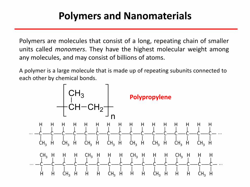
Polymers are molecules that consist of a long, repeating chain of smaller units called monomers. They have the highest molecular weight among any molecules, and may consist of billions of atoms.
A polymer is a large molecule that is made up of repeating subunits connected to each other by chemical bonds.
Polypropylene

Types of Polymers in Everyday Use
Natural (wool, hair, ribber, DNA) and Synthetic Polymers

Polymerization Reactions
Polymerization is the process of combining many small molecules known as monomers into a covalently bonded chain or network.
Synthetic methods are generally divided into two categories, step-growth polymerization and chain-growth polymerization.
Step-growth polymerization refers to a type of polymerization mechanism in which bi-functional or multifunctional monomers react to form first dimers, then trimers, longer oligomers and eventually long chain polymers.
Chain-growth polymerization or chain polymerization is a polymerization technique where unsaturated monomer molecules add onto the active site of a growing polymer chain one at a time. Growth of the polymer occurs only at one (or possibly more) ends.

Properties of Polymers
• Crystallinity (2 and 3D ordering) – x-ray crystallography
• Morphology – SEM and AFM
• Chemical Structure – FTIR, Raman spectroscopy, MS
• Optical Properties – UV/Vis and near-IR spectroscopy
• Tensile Strength (elongation stress) – mechanical testing
• Glass Transition Temperature (amorphous viscous liquid to an amorphous crystalline solid by lowering temperature) – thermal methods of analysis (TGA and DSC).
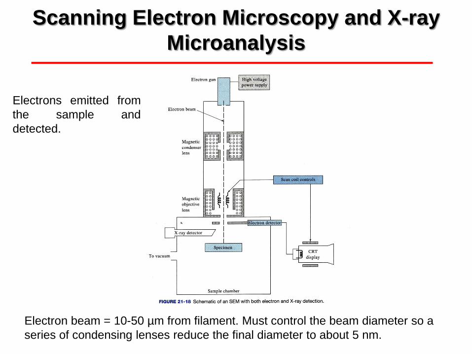
Scanning Electron Microscopy and X-ray
Microanalysis
Electron beam = 10-50 µm from filament. Must control the beam diameter so a
series of condensing lenses reduce the final diameter to about 5 nm.
Electrons emitted from
the sample and
detected.

How Much Energy Does an Accelerated
Electron Beam Possess?
Let’s assume an electron emitted from a sharp
tungsten filament is accelerated to a target using a
voltage of 20 kV.
E = eV where e is the charge of the electron (1.60 x 10-
19 C) and V is the accelerating voltage (V).
E = (1.60 x 10⁻¹⁹ C) (20,000 V) = 3.20 x 10⁻¹⁵ J
Since 1 eV (electron volt) = 1.60 x 10⁻¹⁹ J, then the kinetic
energy of an electron accelerated at 20,000 V is 20,000
eV.

Specimen Interactions with Electron Beam
When the incident electron beam interacts with the same, energy transfer occurs and several processes result to cause the release of lower energy electrons or x-rays that are used for imaging and analysis, respectively.

Specimen Interactions with Electron Beam
Backscattered electrons = electron beam passes close to the positively charged nucleus and is attracted. Beam is deflected without much energy loss. Kinetic energy is unchanged. Larger the Z number the greater the deflection. Atomic number contrast. Secondary electrons = incident electrons knock loosely bound conduction electrons out of the sample. If these weak energy electrons (50 eV) are released near the surface (10 nm) they can be used to image topography. X-ray production = incident electrons excite core electrons. Outer shell or valence electron drop down to fill the vacancy. Excess energy is released as an x-ray characteristic of the Z number of the atom from which it was produced.
Elastic (without energy loss) and inelastic (with energy loss) interactions with the electron beam. The latter is transfer of energy to the solid creating an excited solid.

Cross-Section of the Electron Gun
Filament heated to >2500 K. This causes electron emission from the tip (thermionic emission). If the tip is biased negatively, then the released electrons are repelled from the tip and given an energy proportional to the accelerating voltage = 2-25 kV.
Electron beam focused through electron deflection.

Image is Created by Rastering the
Electron Beam Across the Sample
Electron beam is scanned across the sample. Emitted electrons detected and the image formed.

Important Specimen/Electron
Interactions ---Escape Depth
Greater the energy of the electron beam, the greater the penetration depth. Also depends on atomic density and number of the sample. Better contrast using secondary electrons is possible at lower beam energies.
Best for the sample to be a conductor so as to avoid charging and beam damage. Insulating samples can be coated with a thin layer of metal (Au) to improve image contrast.

Detection of Backscattered Electrons
High energy electron beam (elastically scattered) and wide compared to the incident beam diameter.
Bandgap exists in the
semiconductor. Inelastic
scattering occurs creating an
electron-hole pair. These
charges can be swept away if a
small potential is applied across
the semiconductor. This
produces a photocurrent that is
proportional to the bse intensity.
• Insensitive to lower energy secondary electrons. • Small and robust so they can be located close to the sample.
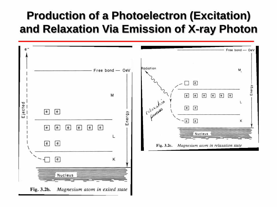
Production of a Photoelectron (Excitation)
and Relaxation Via Emission of X-ray Photon

SEM Images of Polymer Materials
Electrospun polymer for water filtration Superabsorbent polyacrylate
Glass reinforced polypropylene Hollow fiber porous membrane
Public domain images taken from internet

NanoTechnology and Nanomaterials
Nanotechnology is science, engineering, and technology conducted at the nanoscale, which is about 1 to 100 nanometers. (
Nanoscience and nanotechnology involve the ability to see and to control individual atoms and molecules. Synthesis of materials on the nanometer scale.
One nanometer is a billionth of a meter, or 10-9 of a meter. Here are a few illustrative examples: There are 25,400,000 nanometers in an inch. A sheet of newspaper is about 100,000 nanometers thick. On a comparative scale, if a marble were a nanometer, then one meter would be the size of the Earth.

Applications of Nanotechnology in Life
Health care products Targeted drug delivery and imaging
Advanced electronics
Advanced packaging Public domain images taken from internet

Nanotechnology Research
Environmental and Health Risk Assessment
http://www.nano.gov

Relaxation Events Producing an X-ray or
Auger Electron
K shell vacancies are
higher energy than L
shell vacancies.
L shell vacancies are
higher energy than M
shell vacancies.
x-ray = hc/ΔE Δ E = Einner shell – Eouter shell

Typical X-ray Emission Spectrum
Tables of x-ray energies or wavelengths can be used to identify
characteristic peaks – qualitative analysis. Done automatically with
computers.
Only the area of the
sample being scanned by
the electron beam will be
analyzed.

Quantitative Analysis
X-ray count is not a direct indication of concentration. More
information is needed about the spectrometer’s geometry and
about the behavior of the specimen.
X-rays from the near-surface region are emitted without energy loss, whereas those produced deeper in the sample are likely to be absorbed before escaping. Therefore, take-off angle must be known.

Concentrations usually given as atomic percent or weight percent.
Atomic % = # atoms of element x 100
Total # atoms in substance
Weight % = Mass of element x 100
Total mass of substance
1 ppm = 1 part in 106 = mg/kg = 1 x 10⁻⁴%
1 ppb = 1 part in 109 = µg/kg = 1 x 10⁻⁷%