planar antennas for passive uhf rfid tag … in electromagnetics research b, vol. 19, 305{327, 2010...
TRANSCRIPT

Progress In Electromagnetics Research B, Vol. 19, 305–327, 2010
PLANAR ANTENNAS FOR PASSIVE UHF RFID TAG
A. Kumar and D. Parkash
Department of Electronics and Communication EngineeringHaryana College of Technology and ManagementAmbala Road, Kaithal 136027, India
M. V. Kartikeyan
Department of Electronics and Computer EngineeringIIT RoorkeeRoorkee 247667, India
Abstract—In this paper, design, fabrication, and testing of RadioFrequency Identification (RFID) antennas for the European Telecom-munications Standards Institute (ETSI) and Federal CommunicationsCommission (FCC) bands are discussed. The designs proposed in thispaper are for UHF RFID tag that conforms to EPCglobal C1G2 1.2.0.The exceptional characteristics of the RFID are investigated in termsof antenna-IC matching and radiation efficiency. The proposed RFIDantennas have been fabricated on 5 mil thick Flexible Copper CladLaminate and the read range of the proposed RFID antennas is exper-imentally tested. Measured free air read range of all proposed designsis over 4 m. The performance of the tag antenna design affixed to var-ious objects is also tested with read range measurements. The resultsshow that the antenna designs can be used for tagging cardboard andplastic objects.
1. INTRODUCTION
RFID applications are rapidly growing due to drop in both readerand tag prices and expansion of global markets. RFID tags are eitherpowered by the reader (passive tags) or contain on-board power sources(semi-active and active tags). Some estimates indicate that as the pricefor the passive tag continues to fall, virtually every product sold willhave a RFID tag in it. Traditional RFID systems working in the high
Corresponding author: A. Kumar (arun [email protected]).

306 Kumar, Parkash, and Kartikeyan
frequency (HF) and low frequency (LF) bands have limited range dueto their near-field communication constraint. Backscattering RFIDsystems in the ultra high frequency (UHF) band, on the other hand,having the capability to achieve longer range, greater data rate andfaster read speed, have rapidly attracted end users attention in theapplications of supply chain, transportation, etc. [1].
Major hardware components of a RFID system are reader/interro-gator, reader antenna and a RFID tag/transponder. Passive RFID tagsdo not have any internal source of energy. The IC is powered by theelectromagnetic waves radiated by the reader that also communicateswith the tag in order to get its data [2]. Communication in passive UHFRFID systems is based on backscattering of modulated electromagneticwave: Reader transmits energy and commands to tag which thenresponds by backscattering its identification data back to reader usingfor example amplitude shift keying (ASK) modulation [3].
Because in passive RFID tag microchip is attached directly to anantenna, proper impedance match between the antenna and the chipis crucial in RFID tag design [4, 6–10]. It directly influences RFIDsystem performance characteristics such as the range of a tag. Sincenew IC design and manufacturing is a big and costly venture, RFIDtag antennas are designed for an application specific Integrated circuit(ASIC) available in the market. Adding an external matching networkwith lumped elements is usually prohibitive in RFID tags due to costand fabrication issues. To overcome this situation, antenna can bedirectly matched to the ASIC which has complex impedance varyingwith the frequency and the input power applied to the chip [4, 9]. Effectof frequency on microchip input impedance values at various sensitivitylevels is presented in more detail in [9]. To maximize the read rangethe antenna should be conjugate matched to the minimum operationalpower chip impedance [9].
RF tag performance is affected by many factors, including theelectromagnetic properties of objects near or attached to the tagantenna. Often a tuneable antenna design is preferable to providetolerance for tag fabrication variations and for optimizing antennaperformance on different materials in different frequency bands [4].In this paper, we explore structures of planar tag antennas with goodimpedance matching and tuneabilty. The designs presented in thispaper are optimized using EM simulation tool for good free air readrange. Antennas are designed for ETSI frequency band (865.7 MHz to867.6MHz) and FCC frequency band (902.75 MHz to 927.25 MHz) ofUHF RFID. We performed the parametric study of proposed antennadesigns so that tuning parameters of designs can be identified. Oncethe tuning parameters are known, antenna designs can be tuned for

Progress In Electromagnetics Research B, Vol. 19, 2010 307
attaching it on various materials. We have used flexible copper cladlaminate for the designs proposed in this paper because its mechanicalproperties make it very much suitable for mechanically robust andreusable tags for the applications in which RFID tag is to be directlyattached on object without plastic housing.The antennas are designedand analyzed with the aid of IE3D software, which is based on methodof moments (MOM). The finalized designs are built on a 5 mil thickFlexible Copper Clad Laminate. Antenna designs are manufacturedthrough a subtractive process where flexible copper clad laminates arechemically etched to remove all copper except that forming the antennapattern. The prototypes of proposed designs are also tested practicallyusing a UHF reader to check their free air read range and effectof various materials on their performance. Antennas were designedand implemented for NXP UCode Gen2 tag chip with impedance22 − j404Ω at 867MHz and 16 − j380 Ω at 915 MHz measured atminimum operating power. Minimum operating power of NXP UcodeGen2 tag chip at 867MHz and 915 MHz is −14 dBm and −13 dBmrespectively.
2. ANTENNA STRUCTURE
Compared to PET, flexible copper clad laminates have hightensile strength, low dielectric loss, solderability, subtractive processapplicability making it suitable for easy and inexpensive fabricationof RFID antenna. From the cost point of view flexible copper cladlaminate is expensive that PET, but mechanical properties of flexilecopper clad make it suitable for reusable tags which compensate itshigher cost. Antenna pattern on flexible copper clad laminate canbe made using inexpensive screen printing and chemical etching. ByScreen printing a resist on the copper clad was created to protect theantenna pattern in etching. TSSOP8 Chip bonding on flexible copperclad laminate based antenna can be done easily by normal solderingtechnique.
The structure of proposed Antenna 1 is shown in Figure 1.Antenna 1 consists of meandered line feed section, two rectangularsections and two loading bars. Two rectangular sections areincorporated in the design to increase the antenna impedance value.Impedance of Antenna 1 is mainly determined by the two rectangularsections. Two chip pads of size 1.5 mm × 2mm are included inthe design for easy attachment of TSSOP8 packaged microchip.In the proposed design a meandered feed line section is usedbecause meandering allow the antenna to be compact and to provideomnidirectional performance in the plane perpendicular to the axis

308 Kumar, Parkash, and Kartikeyan
of the meander [4, 5, 8]. To have a better control over the antennaimpedance, two loading bar of width 1mm are incorporated in theproposed design. The two loading bars are inductively coupled tofeed line section and a separation of 1mm between loading bars andmeandered feed line section is included. Loading bars in the designhelp in Antenna impedance adjustment which is very important forimpedance matching. Depending upon the chip impedance loadingbars and rectangular sections length can be adjusted to achieve theimpedance matching. Dimensions of the optimized antenna are shownin Figure 1. Physical size of Antenna 1 is 85mm × 16.3mm.
The structure of Antenna 2 is shown in Figure 2. The loadingbar is inductively coupled to radiating section and a separation of0.5mm is kept between loading bars and radiating section. Loadingbar in the proposed design is included for the fine adjustment of theantenna impedance (Ra+jXa Ω). The impedance of antenna is mainlydetermined by the parameters W , Fl, L1, and L2. The geometricparameters are adjusted carefully and final optimized Antenna 2dimensions are: L = 59.5 mm, W = 43 mm, L1 = 22.2mm, L2 =4.39mm, Fl = 38.85, Fw = 0.5mm, Fg = 6.33mm, Lb1 = 62.5mm,Lb2 = 4.25mm. Physical size of Antenna 2 is 62.5 mm × 44.5 mm.
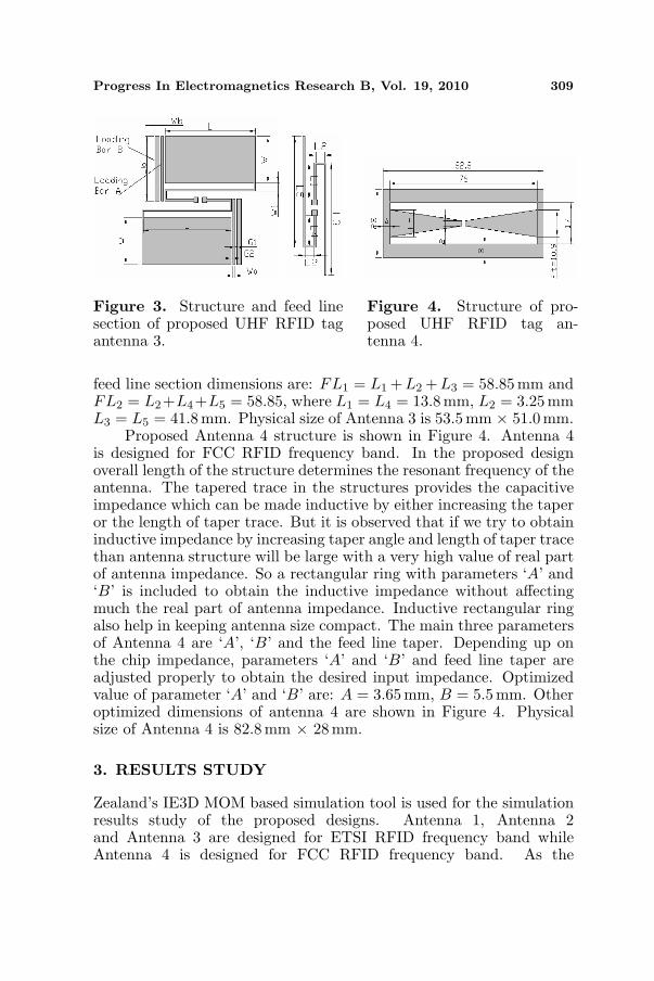
Figure 3 shows the structure of Antenna 3. The two inductivelycoupled loading bars ‘A’ and ‘B’ in the proposed design are includedfor the fine adjustment of the Antenna impedance (Ra + jXa Ω).Meandered feed line section is used to reduce the antenna size [5, 8].The impedance is mainly determined by the geometry parameters L,W and meandered feed line section. Antenna 3 optimized dimensionsare: L = 42.3mm, W = 18.75mm, Lb = 25.75mm, Wa = 1 mm,Wb = 2 mm, W1 = 2.25mm, G1 = 0.9mm, G2 = 0.85mm. Meandered
Figure 1. Structure of proposed UHFRFID tag antenna 1.
Figure 2. Structure ofproposed UHF RFID tagantenna 2.
Progress In Electromagnetics Research B, Vol. 19, 2010 309
Figure 3. Structure and feed linesection of proposed UHF RFID tagantenna 3.
Figure 4. Structure of pro-posed UHF RFID tag an-tenna 4.
feed line section dimensions are: FL1 = L1 + L2 + L3 = 58.85mm andFL2 = L2+L4+L5 = 58.85, where L1 = L4 = 13.8mm, L2 = 3.25mmL3 = L5 = 41.8mm. Physical size of Antenna 3 is 53.5mm × 51.0mm.
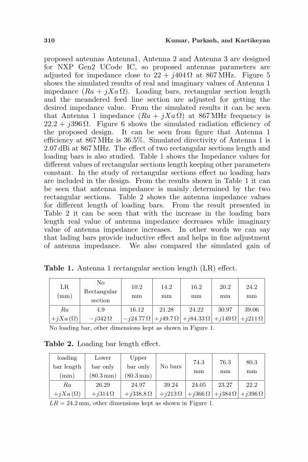
Proposed Antenna 4 structure is shown in Figure 4. Antenna 4is designed for FCC RFID frequency band. In the proposed designoverall length of the structure determines the resonant frequency of theantenna. The tapered trace in the structures provides the capacitiveimpedance which can be made inductive by either increasing the taperor the length of taper trace. But it is observed that if we try to obtaininductive impedance by increasing taper angle and length of taper tracethan antenna structure will be large with a very high value of real partof antenna impedance. So a rectangular ring with parameters ‘A’ and‘B’ is included to obtain the inductive impedance without affectingmuch the real part of antenna impedance. Inductive rectangular ringalso help in keeping antenna size compact. The main three parametersof Antenna 4 are ‘A’, ‘B’ and the feed line taper. Depending up onthe chip impedance, parameters ‘A’ and ‘B’ and feed line taper areadjusted properly to obtain the desired input impedance. Optimizedvalue of parameter ‘A’ and ‘B’ are: A = 3.65mm, B = 5.5mm. Otheroptimized dimensions of antenna 4 are shown in Figure 4. Physicalsize of Antenna 4 is 82.8 mm × 28mm.
3. RESULTS STUDY
Zealand’s IE3D MOM based simulation tool is used for the simulationresults study of the proposed designs. Antenna 1, Antenna 2and Antenna 3 are designed for ETSI RFID frequency band whileAntenna 4 is designed for FCC RFID frequency band. As the
310 Kumar, Parkash, and Kartikeyan
proposed antennas Antenna1, Antenna 2 and Antenna 3 are designedfor NXP Gen2 UCode IC, so proposed antennas parameters areadjusted for impedance close to 22 + j404Ω at 867 MHz. Figure 5shows the simulated results of real and imaginary values of Antenna 1impedance (Ra + jXa Ω). Loading bars, rectangular section lengthand the meandered feed line section are adjusted for getting thedesired impedance value. From the simulated results it can be seenthat Antenna 1 impedance (Ra + jXa Ω) at 867 MHz frequency is22.2 + j396Ω. Figure 6 shows the simulated radiation efficiency ofthe proposed design. It can be seen from figure that Antenna 1efficiency at 867 MHz is 36.5%. Simulated directivity of Antenna 1 is2.07 dBi at 867 MHz. The effect of two rectangular sections length andloading bars is also studied. Table 1 shows the Impedance values fordifferent values of rectangular sections length keeping other parametersconstant. In the study of rectangular sections effect no loading barsare included in the design. From the results shown in Table 1 it canbe seen that antenna impedance is mainly determined by the tworectangular sections. Table 2 shows the antenna impedance valuesfor different length of loading bars. From the result presented inTable 2 it can be seen that with the increase in the loading barslength real value of antenna impedance decreases while imaginaryvalue of antenna impedance increases. In other words we can saythat lading bars provide inductive effect and helps in fine adjustmentof antenna impedance. We also compared the simulated gain of
Table 1. Antenna 1 rectangular section length (LR) effect.
LR
(mm)
No
Rectangular
section
10.2
mm
14.2
mm
16.2
mm
20.2
mm
24.2
mm
Ra
+jXa (Ω)
4.9
−j342Ω
16.12
−j24.77Ω
21.28
+j49.7 Ω
24.22
+j84.33Ω
30.97
+j149Ω
39.06
+j211Ω
No loading bar, other dimensions kept as shown in Figure 1.
Table 2. Loading bar length effect.
loading
bar length
(mm)
Lower
bar only
(80.3mm)
Upper
bar only
(80.3mm)
No bars74.3
mm
76.3
mm
80.3
mm
Ra
+jXa (Ω)
26.29
+j314Ω
24.97
+j338.8Ω
39.24
+j213Ω
24.05
+j366Ω
23.27
+j384Ω
22.2
+j396Ω
LR = 24.2mm, other dimensions kept as shown in Figure 1.

Progress In Electromagnetics Research B, Vol. 19, 2010 311
0.860 0.865 0.870 0.875 0.880
0
50
100
150
200
250
300
350
400
Ante
nna
Imped
ance
(Ra+
jXa)
Frequency (GHz)
Ra
Xa
Figure 5. Simulated results of antenna 1 impedance.
0.860 0.865 0.870 0.875 0.880
35.8
36.0
36.2
36.4
36.6
36.8
37.0
37.2
37.4
Rad
aiti
on E
ffic
iency
(%
)
Frequency (GHz)
Figure 6. Simulated results of antenna 1 radiation efficiency.
Antenna 1 and a simple meander line dipole and observed that gainparameter of a simple meander line dipole is less than the Antenna 1gain parameter. It shows that two rectangular sections in Antenna 1helped in increasing the gain or effective area of the Antenna 1.
Figure 7 shows the simulated return loss of the optimized designwhen the antenna is conjugate-matched with the commercial tag chip(NXP Ucode). The simulated bandwidth is 2% (S11 ≤ −10 dB) from863 to 880MHz, a 17 MHz bandwidth. ETSI frequency band for UHFRFID is from 865.7 MHz to 867 MHz.

312 Kumar, Parkash, and Kartikeyan
0.860 0.865 0.870 0.875 0.880
-35
-30
-25
-20
-15
-10
-5
S1
1,
dB
Frequency, GHz
Figure 7. Simulated return loss versus frequency plot of antenna 1.
= 0º = 90ºϕ ϕ
Figure 8. Elevation pattern display of antenna 1.
In Figure 8, the 2-D radiation plots are shown. The 2-D polar plotshows the radiation in the two different planar cuts for the x-z plane(ϕ = 0deg) and the y-z plane (ϕ = 90 deg) with angle θ that variesfrom 0 to 360 degrees. The pattern has two nulls in the whole 360

Progress In Electromagnetics Research B, Vol. 19, 2010 313
degree coverage area. This pattern similar to the radiation pattern ofa half-wavelength dipole antenna as antenna 1 is also a dipole antenna.
Figure 9 shows the simulated results of real and imaginaryvalues of Antenna 2 impedance (Ra + jXa Ω). From the simulatedimpedance versus frequency graph it can be seen that Antenna 2impedance (Ra + jXa Ω) at 867MHz frequency is 22.83 + j400.8Ω.From simulation results study it is observed that Loading bar length(Lb = Lb1 + Lb2) helps in fine adjustment of imaginary part (Xa) ofthe antenna impedance. Loading bar length has very small effect onreal part of impedance (Ra). Xa values for different loading bar lengthkeeping all other parameters constant are presented in Table 3. Effectof other parameter Fl, L1 and W are presented in Tables 4–6. Fromthe results shown in Tables 4–6 it is clear that antenna impedanceis very much affected by Fl, L1, and W . It can be seen from theresults that geometry parameter W has slight effect on real part of
Table 3. Effect of loading bar length Lb on antenna impedance.
(Lb)
mmNo bar
Lb1 = L
mm
Lb2 = 0
mm
Lb1 = 62.5
mm
Lb2 = 0
mm
Lb1 = 62.5
mm
Lb2 = 1.25
mm
Lb1 = 62.5
mm
Lb2 = 3.25
mm
Lb1 = 62.5
mm
Lb2 = 4.25
mm
jXa
(Ω)j312.7Ω j382.5Ω j384.1Ω j387.2Ω j395.5Ω j400.8Ω
L = 59.5mm, W = 43mm, L1 = 22.2mm, L2 = 4.39mm, Fl = 38.85,Fw = 0.5mm, Fg = 6.33mm.
Table 4. Effect of feed line length Fl on antenna impedance.
Fl (mm) 38.5mm 36.5mm 34.5mm 32.5mm 30.5mm
Ra
+jXa Ω
22
+j400.8Ω
20.56
+j367Ω
18.66
+335.6Ω
17.02
+j335.6Ω
15.63
+j278.6Ω
L = 59.5mm, W = 43 mm, L1 = 22.2mm, L2 = 4.39mm, Fw = 0.5mm,Fg = 6.33mm, Lb = 63.13, Lb1 = 5.25mm.
Table 5. Effect of rectangular section length L1 on antenna impe-dance.
L1 (mm) 22.2mm 21.2mm 20.2mm 19.2mm 18.2 mm
Ra
+jXa (Ω)
22
+j400.8Ω
21
+j380.4 Ω
19.96
+366.8Ω
19.55
+j356.9Ω
18.59
+j344.6Ω
L = 59.5mm, W = 43mm, L2 = 4.39mm, Fl = 38.85, Fw = 0.5mm,Fg = 6.33mm, Lb = 63.13, Lb1 = 5.25mm

314 Kumar, Parkash, and Kartikeyan
Table 6. Effect of rectangular section width W on antenna impedance.
W (mm) 43mm 42mm 41mm 40mm 39mm
Ra
+jXa Ω
22
+j400.8Ω
21.71
+j352.6Ω
21.3
+328.8Ω
20.99
+j311.7Ω
20.65
+j297Ω
L = 59.5mm, L1 = 22.2mm, L2 = 4.39 mm, Fl = 38.85, Fw = 0.5mm,Fg = 6.33mm, Lb = 63.13, Lb1 = 5.25mm.
0.850 0.855 0.860 0.865 0.870 0.875 0.880
0
50
100
150
200
250
300
350
400
450
Ra +
jX
a
Frequency, GHz
Ra
Xa
Figure 9. Simulated results of antenna 2 impedance.
antenna impedance while its effect on imaginary value is considerable.It can also be seen from the results that feed line length Fl effecton real part of antenna impedance is more than the other geometryparameters. Figure 10 shows the simulated radiation efficiency of theproposed design. It can be seen from figure that Antenna 2 efficiencyat 867 MHz is 35%. Simulated directivity of antenna 2 is 1.92 dBi at867MHz.
Figure 11 shows the simulated return loss of the optimized design.The simulated results shows that antenna bandwidth (S11 ≤ −10 dB)is from 860 to 877 MHz, and capable to cover to ETSI frequency bandfor UHF RFID.
Radiation plots of antenna 2 in two different planar cuts for thex-z plane (ϕ = 0 deg) and the y-z plane (ϕ = 90deg) are shown inFigure 12. The 2-D polar plot shows that the pattern has two nullsin the whole 360 degree coverage area. Antenna 2 pattern is similarto the radiation pattern of a half-wavelength dipole antenna becauseantenna 2 structure is like a bent dipole antenna.

Progress In Electromagnetics Research B, Vol. 19, 2010 315
0.850 0.855 0.860 0.865 0.870 0.875 0.880
33.5
34.0
34.5
35.0
35.5
36.0
36.5
Rad
iati
on E
ffic
iency
, %
Frequency, GHz
Figure 10. Simulated results of antenna 2 radiation efficiency.
0.850 0.855 0.860 0.865 0.870 0.875 0.880
-35
-30
-25
-20
-15
-10
-5
0
S1
1,
dB
Frequency, GHz
Figure 11. Simulated return loss versus frequency plot of antenna 2.
Table 7. Effect of rectangular section length L on antenna impedance.
L (mm) 37.3mm 39.3mm 40.3mm 41.3mm 42.3mmRa
+jXa (Ω)20.9
+j321.7Ω21.6
+j347 Ω22.11
+j364.8Ω22.67
+j383.3Ω23.34
+j404ΩW = 18.75mm, Lb = 25.75mm, Wa = 1mm, Wb = 2mm, W1 = 2.25mm,G1 = 0.9mm, G2 = 0.85mm, FL1 = 58.85mm and FL2 = 58.85.

316 Kumar, Parkash, and Kartikeyan
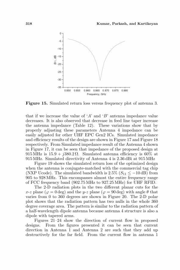
Simulated impedance of Antenna 3 is shown in Figure 13.Simulated impedance of proposed Antenna 3 design at 867 MHz is23.34 + j404Ω. Effect of geometry parameter L and W are shown inTable 7 and Table 8. From the results it can be seen that effect of L andW on imaginary part of impedance is almost similar, but W variationshave more effect on real part of impedance than the L variations. Feedline variation effect is shown in Table 9. Loading bars ‘A’ and ‘B’ helpsin fine adjustment of the antenna impedance. Simulated radiationefficiency of Antenna 3 is 70% at 867 MHz (Figure 14). Simulateddirectivity of antenna 3 is 2.14 dBi at 867 MHz. Simulated return loss ofthe optimized design is shown in Figure 15. The simulated bandwidthis from 860 to 873 MHz (S11 ≤ −10 dB), and completely covers theETSI frequency band (865.7 MHz to 867 MHz) for UHF RFID.
In Figure 16, the 2-D radiation plots are shown. The 2-D polarplot shows the radiation in the two different planar cuts for the x-
= 0º = 90ºϕ
ϕ
Figure 12. Elevation pattern display of antenna 2.
Table 8. Effect of rectangular section width W on antenna impedance.
W (mm) 14.75mm 15.75mm 16.75mm 17.75mm 18.75mmRa
+jXa (Ω)16.45
+j330.7Ω17.97
+j349Ω19.63
+j367.6Ω21.42
+j386Ω23.34
+j404ΩL = 42.3mm, Lb = 25.75mm, Wa = 1mm, Wb = 2 mm, W1 = 2.25mm,G1 = 0.9mm, G2 = 0.85mm, FL1 = 58.85mm and FL2 = 58.85.

Progress In Electromagnetics Research B, Vol. 19, 2010 317
z plane (ϕ = 0 deg) and the y-z plane (ϕ = 90deg) with angleθ that varies from 0 to 360 degrees. The pattern is similar tothe radiation pattern of a half-wavelength dipole antenna becauseantenna 3 structure is also like a bent dipole antenna.
Antenna 4 is designed for FCC RFID frequency band. NXPGen2 Ucode IC provide impedance 16 − j380Ω at 915 MHz, soAntenna 4 parameters ‘A’, ‘B’ and feed line taper are adjusted toget antenna impedance close to 16 + j380. It is observed from thestudy of effect of parameter ‘A’ and ‘B’ (Table 10 and Table 11)
0.864 0.865 0.866 0.867 0.868
0
50
100
150
200
250
300
350
400
Ra
+ jX
a
Frequency, GHz
Ra
Xa
Figure 13. Simulated results of antenna 3 impedance.
0.864 0.865 0.866 0.867 0.868
70.00
70.02
70.04
70.06
70.08
Rad
iati
on E
ffic
iency
, %
Frequency, GHz
Figure 14. Simulated results of antenna 3 radiation efficiency.
318 Kumar, Parkash, and Kartikeyan
0.850 0.855 0.860 0.865 0.870 0.875 0.880
-35
-30
-25
-20
-15
-10
-5
0
S1
1, dB
Frequency, GHz
Figure 15. Simulated return loss versus frequency plot of antenna 3.
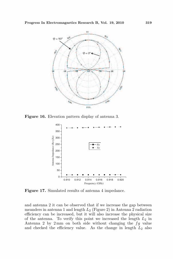
that if we increase the value of ‘A’ and ‘B’ antenna impedance valuedecreases. It is also observed that decrease in feed line taper increasethe antenna impedance (Table 12). These variations show that byproperly adjusting these parameters Antenna 4 impedance can beeasily adjusted for other UHF EPC Gen2 ICs. Simulated impedanceand efficiency results of the design are shown in Figure 17 and Figure 18respectively. From Simulated impedance result of the Antenna 4 shownin Figure 17, it can be seen that impedance of the proposed design at915MHz is 15.9 + j380.2Ω. Simulated antenna efficiency is 60% at915MHz. Simulated directivity of Antenna 4 is 2.36 dBi at 915 MHz
Figure 19 shows the simulated return loss of the optimized designwhen the antenna is conjugate-matched with the commercial tag chip(NXP Ucode). The simulated bandwidth is 2.5% (S11 ≤ −10 dB) from905 to 928 MHz. This encompasses almost the entire frequency rangeof FCC frequency band (902.75MHz to 927.25 MHz) for UHF RFID.
The 2-D radiation plots in the two different planar cuts for thex-z plane (ϕ = 0 deg) and the y-z plane (ϕ = 90deg) with angle θ thatvaries from 0 to 360 degrees are shown in Figure 20. The 2-D polarplot shows that the radiation pattern has two nulls in the whole 360degree coverage area. The pattern is similar to the radiation pattern ofa half-wavelength dipole antenna because antenna 4 structure is also adipole with tapered arms.
Figures 21–24 show the direction of current flow in proposeddesigns. From the figures presented it can be seen that currentdirection in Antenna 1 and Antenna 2 are such that they add updestructively for the far field. From the current flow in antenna 1
Progress In Electromagnetics Research B, Vol. 19, 2010 319
= 0º
= 90º
ϕ
ϕ
Figure 16. Elevation pattern display of antenna 3.
0.910 0.912 0.914 0.916 0.918 0.920
0
50
100
150
200
250
300
350
400
Ante
nna
Imped
ance
(Ra+
jXa)
Frequency (GHz)
Ra
Xa
Figure 17. Simulated results of antenna 4 impedance.
and antenna 2 it can be observed that if we increase the gap betweenmeanders in antenna 1 and length L2 (Figure 2) in Antenna 2 radiationefficiency can be increased, but it will also increase the physical sizeof the antenna. To verify this point we increased the length L2 inAntenna 2 by 2 mm on both side without changing the fg valueand checked the efficiency value. As the change in length L2 also

320 Kumar, Parkash, and Kartikeyan
0.910 0.912 0.914 0.916 0.918 0.920
59.0
59.5
60.0
60.5
61.0
Rad
iati
on E
ffic
iency
(%
)
Frequency (GHz)
Figure 18. Simulated results of antenna 4 radiation efficiency.
0.84 0.86 0.88 0.90 0.92 0.94 0.96
-25
-20
-15
-10
-5
0
S11
, d
B
Frequency, GHz
Figure 19. Simulated return loss versus frequency plot of antenna 4.
changes the impedance value so we adjusted Fl parameter to obtainthe conjugate matching. We obtained a 39.6% simulated efficiencyvalue which is 5% more than the previous value of simulated efficiency.Major factor for the high efficiency of antenna 3 and antenna 4 isbecause of the way the current flow. Since the direction of currentflow in Antenna 3 and antenna 4 add up constructively for far-fieldradiation, the radiation efficiency of Antenna 3 and Antenna 4 is morethan the antenna efficiency of Antenna 1 and Antenna 2.
A theoretical read range study of all proposed designs is also doneon the basis of obtained simulated radiation efficiency and simulated

Progress In Electromagnetics Research B, Vol. 19, 2010 321
= 0º = 90ºϕ ϕ
Figure 20. Elevation pattern display of antenna 4.
Figure 21. Simulated current flow in antenna 1.
Table 9. Effect of meandered feed line section length on antennaimpedance.
FL1 & FL2
(mm)
L1=L4=9.8
mm
L3=L5=37.8
mm
L1=L4=10.8
mm
L3=L5=38.8
mm
L1=L4=11.8
mm
L3=L5=39.8
mm
L1=L4=12.8
mm
L3=L5=40.8
mm
L1=L4=13.8
mm
L3=L5=41.8
mm
Ra+jXa
(Ω)
15.81+j286
Ω
17.07+j310
Ω
18.58+j335.3
Ω
20.48+j365.4
Ω
23.34+j404
Ω
L = 42.3mm, W = 18.75mm, Lb = 25.75 mm, Wa = 1 mm, Wb = 2mm, W1 =2.25mm, G1 = 0.9mm, G2 = 0.85mm, L2 = 3.25mm.

322 Kumar, Parkash, and Kartikeyan
Figure 22. simulated current flow in antenna 2.
Figure 23. simulated current flow in antenna 3.
Figure 24. simulated current flow in antenna 4.
directivity. The read range is calculated using the free space formula [4]
r =λ
4π
√PtGtGrpτ
Pth

Progress In Electromagnetics Research B, Vol. 19, 2010 323
Table 10. Effect of parameter ‘A’.
A (mm) 3.65mm 4.65mm 5.65mm 7.65mm 9.65mm 11.65mm
Ra
+jXa (Ω)
15.93
+j380.2Ω
14.7
+j362.5Ω
13.28
+j345.3 Ω
11.59
+j317.4Ω
10.1
+j291Ω
8.55
+j265.6Ω
Antenna length = 82.8 mm, Antenna width = 28 mm, Ft = 10.9mm, B = 5.5mm.
Table 11. Effect of parameter ‘B’.
B (mm) 5.5mm 6.5mm 7.5mm 4.5mm 3.5mm 3.9mm
Ra
+jXa (Ω)
15.93
+j380.2Ω
11.39
+j328.6Ω
8.74
+j284.2Ω
23.22
+j440Ω
36.28
+j521Ω
19.96
+j515Ω
Antenna length = 82.8 mm, Antenna width = 28 mm, Ft = 10.9mm,A = 3.65mm.
Table 12. Effect of feed line taper.
Ft (mm) 10.9mm 9.9mm 8.9mm 7.9mm 5.9mm 3.9mm
Ra
+jXa (Ω)
15.93
+j380.2Ω
16.19
+j393Ω
16.84
+j410Ω
17.35
+j427Ω
18.46
+j465Ω
19.96
+j515Ω
Antenna length = 82.8mm, Antenna width = 28mm, A = 3.65mm,B = 5.5mm.
where λ is the wavelength, Pt is the power transmitted by the reader,Gt is the gain of the transmitting antenna, Gr is the gain of thereceiving tag antenna, Pth is the minimum threshold and p is thepolarization efficiency which should be 1/2 for most conventional caseof circular-to-linear polarization mismatch. τ is the power transmissioncoefficient given by
τ =4RcRa
|Zc + Za|2 , 0 ≤ τ ≤ 1
where Zc = Rc+jXc is chip impedance and Za = Ra+jXa is antennaimpedance. Theoretically calculated results based on above formulasare shown in Table 13.
Table 13. Theoretically calculated read range.
PtGt (W) Theoretically calculated Read range (m)Antenna 1 3.3W 4.32 mAntenna 2 3.3W 4.1mAntenna 3 3.3W 5.9mAntenna 4 4W 5.3m

324 Kumar, Parkash, and Kartikeyan
4. FABRICATION AND TEST RESULTS
The proposed antennas are fabricated by flexible copper clad laminatewith εr = 3.5 and thickness 5 mil. Simple screen printing and chemicaletching is used for fabrication. Prototypes of proposed antennas areshown in Figure 25 and Figure 26. Chip is attached to the antennasby manual soldering. Fabricated antennas performance is judgedby testing their read range performance. Read range performanceof the proposed antenna designs is measured with the help of SiritIN510 fixed Reader and a single, circularly polarized antenna, ofgain 6.5 dBi. Both reader and antenna can operate in 860 MHz to960MHz frequency band. The reader automatically calculates theconducted power level for reader antenna based on the regulatoryregion. The calculation takes into account antenna gain and cableloss settings. Conducted power level variation is required because asper the European Telecommunications Standards Institute (ETSI) andFederal Communications Commission (FCC) regulations maximum
Figure 25. Prototype of the proposed antenna 1 and antenna 2.
Figure 26. Prototype of the proposed antenna 3 and antenna 4.

Progress In Electromagnetics Research B, Vol. 19, 2010 325
allowed effective isotropic radiated power (EIRP) ratings are 3.3W(or 2 W ERP) and 4W respectively. For read range measurementof Antenna 1–Antenna 3 RFID reader is set to ETSI frequencyband (865.7 MHz–867 MHz) and to FCC frequency band (902.75 MHz–927.25MHz) for Antenna 4. Measurement set up was installed in anempty big hall. For free air read range measurement antennas wereattached to very thin strings in a plastic frame. To find out the readdistance the tag was first kept at very large distance from the readerand moved slowly towards the reader antenna. The distance at whichreader detected the tag continuously was measured and recorded. Werepeated the same procedure 5–6 times for each tag to verify the result.
RF tag performance is affected by many factors, including theelectromagnetic properties of objects near or attached to the tagantenna. Since the resonance frequency of antenna changes whenplaced on a material, so many common materials have strong effectson the performance of UHF tag antenna. In worst case, tags maybecome unreadable ([11, 12]). To test the Effect of various materialson read range of the proposed designs we also measured the read rangeof the designs by attaching the antennas on plastic box, cardboardbox and wooden box. We also tested the near metal performance ofthe proposed designs. The measured results are presented in Table 14.From the result presented in Table 14 it can be seen that free airread range of all designs proposed in this paper is good. Antenna 1sensitivity is very high comparatively to other designs. If we comparethe on plastic read range of Antenna 2–Antenna 4 designs it can beseen that plastic material have not much effect on proposed antennasresonance frequency and that is why antennas performance on plasticis comparable to their free air read range performance. In case of cardboard read range of Antenna 1–antenna 3 has reduced to 50%–60%than their read range in free space and on plastic box. It means cardboard have considerable effect on antennas impedance value. Thereis no effect of card board on read range of antenna 4. Antenna 1–antenna 3 performance on wood and near metal surface is very poor,which means wood and metal have very major effect on antennasresonance frequency. Antenna 4 performance on wood and near metalis acceptable. Less sensitivity of antenna 4 comparatively to otherproposed designs may be because of the large FCC bandwidth ofreader. For measurement of antenna 4 reader is set for frequency band902.75MHz–927.25MHz. So even after the shift in resonance frequencyof antenna 4, due to the materials effect, shifted resonant frequency ofantenna 4 may lie with in the bandwidth range of reader. Large readrange of antenna 4 comparatively to other proposed designs can alsobe due to the reason that allowable EIRP is more in FCC band than

326 Kumar, Parkash, and Kartikeyan
the ETSI band. From the measured results it is clear that proposeddesigns provide acceptable read range for cardboard and plastic boxand need tuning to get good read range for various materials in specificfrequency band. Tuning of proposed designs for various materials is tobe carried out in future work.
A comparison between theoretical (Table 13) and experimentally(Table 14) measured read range for all the proposed tags showsthat theoretical data and experimental data are in close agreement.Measured values of Antenna 1, Antenna 2 and Antenna 4 are more thantheoretically calculated value while Antenna 3 has shown an oppositebehavior. Antenna 3 measured read range is less than the expectedvalue which may be due to the shift in resonant frequency after thefabrication. As the simulated directivity of all proposed designs isapproximately same, so it can be said that higher radiation efficiencycan help in getting larger read range.
Table 14. Measured results of proposed antennas.
Free AirOn Card
Board
On
wood
On
Plastic
Near Metal
(10mm above
from the metal
surface)
Antenna 1 17.25m 3m 1m 2m 0.3m
Antenna 2 5m 3.5m 1m 5m 0.45m
Antenna 3 4.5m 2.5m 1m 4.25 m 0.02m
Antenna 4 7m 7.5m 5m 8m 3m
5. CONCLUSION
Four passive RFID tag antenna Designs for ETSI and FCC UHF RFIDfrequency bands are proposed. All the designs are simulated to havegood conjugate matching to commercially available NXP Gen2 UCodeChip. Low cost Flexible Copper Clad Laminate is used for prototypesfabrication. The prototypes of the designs are fabricated and testedfor read range performance. Read range is measured by attachingthe antennas on various objects for checking the material dependencyon antennas performance. Measured results shows that the proposedantenna designs can be used for UHF RFID application. From thesimulation studies it is clear that all the antennas have various tuningparameters which can be adjusted properly for optimizing antennaperformance on different materials. From the measured results we cansay that proposed designs with the dimensions mentioned in this paperare suitable for RFID tagging on cardboard and plastic boxes.

Progress In Electromagnetics Research B, Vol. 19, 2010 327
REFERENCES
1. Finkenzeller, K., RFID Handbook: Fundamentals and Applica-tions in Contactless Smart Cards and Identification, John Wiley& Sons Ltd., West Sussex, Englnad, 2003.
2. Curty, J.-P., M. Declercq, C. Dehollain, and N. Joehl, Design andOptimization of Passive RFID System, Springer, New York, USA,2007.
3. Ukkonen, L., M. Schaffrath, D. W. Engels, L. Sydanheimo, andM. Kivikoski, “Operability of folded microstrip patch-type tagantenna in the UHF RFID bands within 865–928MHz,” IEEEAntennas and Wireless Propagation Letters, Vol. 5, 414–417, 2006.
4. Rao, K. V. S., P. V. Nikitin, and S. F. Lam, “Antenna designfor UHF RFID tags: A review and a practical application,” IEEETransactions on Antennas and Propagation, Vol. 53, No. 12, 3870–3876, 2005.
5. Kwon, H. and B. Lee, “Meander line RFID tag at UHF bandevaluated with radar cross sections,” APMC Proceedings, 2005.
6. Diugwu, C. A., J. C. Batchelor, R. J. Langley, and M. Fogg,“Planar antenna for passive radio frequency identification [RFID]tags,” IEEE Africon, 2004.
7. Son, H. W. and C. S. Pyo, “Design of RFID tag antennas usingan inductively coupled feed,” Electronics Letters, Vol. 41, No. 18,2005.
8. Gaetano, M., “The art of UHF RFID antenna design: Impedance— Matching and size reduction techniques,” IEEE Antennas andPropagation Magazine, Vol. 50, No. 1, 66–79, 2008.
9. Loo, C. H., K. Elmahgoub, F. Yang, A. Elsherbeni, D. Kajfez,A. Kishk, and T. Elsherbeni, “Chip impedance matching forUHF RFID tag antenna design,” Progress In ElectromagneticsResearch, PIER 81, 359–370, 2008.
10. Nikitin, P. V. and K. V. S. Rao, “Antennas and propagation inUHF RFID systems,” 2008 IEEE International Conference onRFID The Venetian, 277–288, Las Vegas, Nevada, USA, Apr. 16–17, 2008.
11. Dobkin, D. M. and S. M. Weigand, “Environmental effects onRFID tag antennas,” Proc. IEEE Int. Microw. Symp., Jun. 2005.
12. Griffin, J. D., G. D. Durgin, A. Haldi, and B. Kippelen, “RFtag antenna performance on various materials using radio linkbudgets,” IEEE Antennas and Wireless Propagation Letters,Vol. 5, 2006.