piml plus hw specification
TRANSCRIPT

PIML plus HW spec Feb.2007
PIML plus HW Specification
Revision: Preliminary Date: February 5, 2007
This document is the sole and exclusive property of TechFaith Wireless. Not to be distributed or divulged without prior written agreement. Page: 1 / 73
PIML plus HW spec Feb.2007
Document Information
Revision Date History of the evolution Draft vision Feb 2007 Creation as “Draft”
Overview
This document defines and specifies the TECHFAITH WIRELESS PIML plus module with 32 Mb of Flash memory and 8 Mb of SRAM (32/8), which support GSM/GPRS function.
This document is the sole and exclusive property of TechFaith Wireless. Not to be distributed or divulged without prior written agreement. Page: 2 / 73

PIML plus HW spec Feb.2007
Contents
Document Information........................................................................................................................ 2
Overview.................................................................................................................................................... 2
Caution........................................................................................................................................................ 6
Trademarks................................................................................................................................................ 6
1 General description ...................................................................................................................................... 7 1.1 General information .......................................................................................................................... 7 1.2 Function description.......................................................................................................................... 8
1.2.1 RF functionalities ................................................................................................................... 9 1.2.2 Baseband functionalities......................................................................................................... 9
1.3 Firmware ........................................................................................................................................... 9 2 Interfaces .................................................................................................................................................... 10
2.1 General Purpose Connector (GPC) ................................................................................................. 10 2.2 Power supply ................................................................................................................................... 10
2.2.1 Power supply description ..................................................................................................... 10 2.2.2 Power consumption .............................................................................................................. 12
2.3 Electrical information for digital I/O............................................................................................... 14 2.4 LCD interface.................................................................................................................................. 15
2.4.1 I2C interface.......................................................................................................................... 15 2.5 Keyboard interface .......................................................................................................................... 16 2.6 Main Serial link (UART1)............................................................................................................... 18
2.6.1 Typical implementation with a RS232 Terminal .................................................................. 19 2.6.2 Typical implementation with a microprocessor.................................................................... 20
2.7 SIM interface................................................................................................................................... 21 2.7.1 General Description.............................................................................................................. 21 2.7.2 SIM socket connection ......................................................................................................... 23
2.8 General Purpose Input/Output.................................................................................................... 24 2.9 Analog to Digital Converter ......................................................................................................... 25
2.9.1 How to define R1 and C1 ..................................................................................................... 26 2.10 Audio interface .............................................................................................................................. 27
2.10.1 Main audio interface........................................................................................................... 27 2.10.1.1 Main Microphone Inputs (MIC2) ............................................................................ 27 2.10.1.2 Main speaker outputs (SPK2).................................................................................. 28
2.10.2 Auxiliary audio interface .................................................................................................... 29 2.10.2.1 Auxiliary Microphone Inputs (MIC1) ..................................................................... 30 2.10.2.1.1 Differential connection......................................................................................... 30 2.10.2.1.2 Single-ended connection ...................................................................................... 32
This document is the sole and exclusive property of TechFaith Wireless. Not to be distributed or divulged without prior written agreement. Page: 3 / 73
PIML plus HW spec Feb.2007
2.10.2.1.3 Auxiliary speaker outputs characteristics ............................................................. 33 2.10.3 Buzzer Output..................................................................................................................... 33
2.11 Battery charging interface ............................................................................................................. 34 2.11.1 Li-ion charging procedure ............................................................................................. 35
2.12 ON / OFF............................................................................................................................... 36 2.12.1 Operating sequences..................................................................................................... 36
2.12.1.1 Power ON................................................................................................................ 36 2.12.1.2 Power OFF .............................................................................................................. 37 2.12.2 Reset signal (~RST) ................................................................................................... 38 2.12.2.1 Reset sequence ........................................................................................................ 39
2.13 External Interrupt (~INTR) ...................................................................................................... 40 2.14 VCC output ................................................................................................................................... 40 2.15 VCC_RTC (REAL TIME CLOCK SUPPLY)............................................................................ 41
2.15.1 Interface description ........................................................................................................... 41 2.15.2 Typical implementation: ........................................................................................ 42
2.15.2.1 Capacitor ................................................................................................................. 42 2.15.2.2 Super Capacitor ....................................................................................................... 42 2.15.2.3 Battery cell with regulator ....................................................................................... 43 2.15.2.4 Non Rechargeable battery ....................................................................................... 43
2.16 RF interface ................................................................................................................................... 44 2.16.1 RF connection .................................................................................................................... 44 2.16.2 RF performances ................................................................................................................ 46 2.16.3 Antenna specifications........................................................................................................ 46
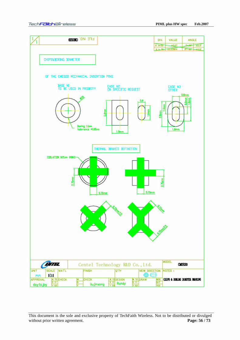
3 Technical specifications ............................................................................................................................. 47 3.1 Interface........................................................................................................................................... 47 3.2 Environmental Specifications..................................................................................................... 50 3.3 Mechanical specifications ............................................................................................................... 51
3.3.1 Physical characteristics......................................................................................................... 51 3.3.2 Mechanical drawings............................................................................................................ 51
4 Connectors and peripheral devices references ........................................................................................... 53 4.1 General Purpose Connector............................................................................................................. 53 4.2 SIM Card Reader............................................................................................................................. 53 4.3 Microphone ..................................................................................................................................... 53 4.4 Speaker............................................................................................................................................ 54 4.5 Antenna Cable ................................................................................................................................. 54 4.6 GSM antenna................................................................................................................................... 54
5 Design Guidelines ...................................................................................................................................... 54 5.1 Hardware and RF ............................................................................................................................ 54
5.1.1 EMC recommendations........................................................................................................ 54 5.1.2 Power Supply ....................................................................................................................... 55 5.1.3 Layout requirement .............................................................................................................. 55 5.1.4 Antenna................................................................................................................................. 57
This document is the sole and exclusive property of TechFaith Wireless. Not to be distributed or divulged without prior written agreement. Page: 4 / 73

PIML plus HW spec Feb.2007
5.2 Mechanical integration .................................................................................................................... 57 5.3 Firmware upgrade ........................................................................................................................... 57
5.3.1 Nominal upgrade procedure ................................................................................................. 57 5.3.2 Backup procedure................................................................................................................. 58 5.3.3 TechFaith PMIL Module Application Notes ........................................................................ 58
6 Appendix .................................................................................................................................................... 59 6.1 TECHFAITH WIRELESS acceptance test...................................................................................... 59 6.2 Standards and Recommendations.................................................................................................... 61 6.3 Safety recommendations (for information only) .......................................................................... 63
6.3.1 RF safety............................................................................................................................ 63 6.3.1.2 Exposure to RF energy .............................................................................................. 63 6.3.1.3 Efficient terminal operation.................................................................................... 64 6.3.1.4 Antenna care and replacement................................................................................... 64
6.3.2 General safety ................................................................................................................... 65 6.3.2.1 Driving ...................................................................................................................... 65 6.3.2.2 Electronic devices...................................................................................................... 65 6.3.2.3 Vehicle electronic equipment..................................................................................... 65 6.3.2.4 Medical electronic equipment ................................................................................... 65 6.3.2.5 Aircraft ...................................................................................................................... 65 6.3.2.6 Children..................................................................................................................... 66 6.3.2.7 Blasting areas ............................................................................................................ 66 6.3.2.8 Potentially explosive atmospheres ............................................................................ 66
6.4 Application notes for the SIM interface .......................................................................................... 67 6.5 General Purpose Connector data sheet ............................................................................................ 67
This document is the sole and exclusive property of TechFaith Wireless. Not to be distributed or divulged without prior written agreement. Page: 5 / 73

PIML plus HW spec Feb.2007
Caution
Information furnished herein by TECHFAITH WIRELESS is accurate and reliable. However no responsibility is assumed for its use. Please read carefully the safety precautions for a terminal based on TECHFAITH WIRELESS PIML plus module.
Trademarks
Some mentioned products are registered trademarks of their respective companies.
This document is the sole and exclusive property of TechFaith Wireless. Not to be distributed or divulged without prior written agreement. Page: 6 / 73
PIML plus HW spec Feb.2007
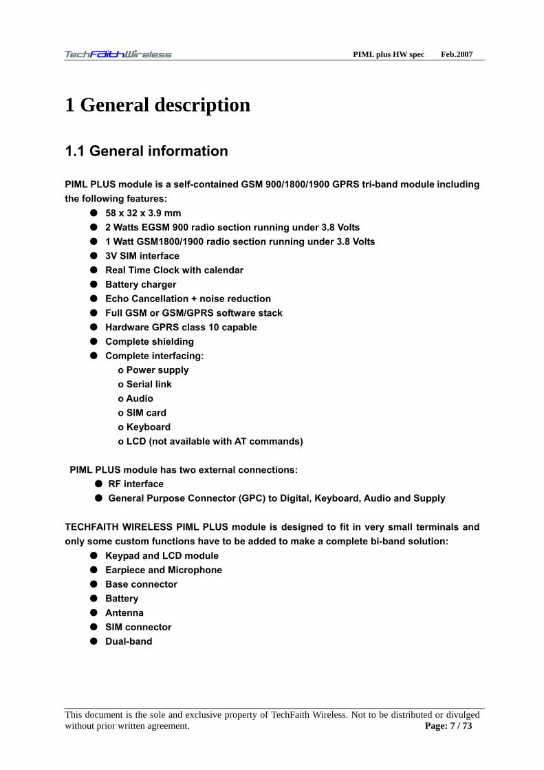
1 General description
1.1 General information
PIML PLUS module is a self-contained GSM 900/1800/1900 GPRS tri-band module including the following features:
58 x 32 x 3.9 mm 2 Watts EGSM 900 radio section running under 3.8 Volts 1 Watt GSM1800/1900 radio section running under 3.8 Volts 3V SIM interface Real Time Clock with calendar Battery charger Echo Cancellation + noise reduction Full GSM or GSM/GPRS software stack Hardware GPRS class 10 capable Complete shielding Complete interfacing: o Power supply
o Serial link o Audio o SIM card o Keyboard o LCD (not available with AT commands) PIML PLUS module has two external connections: RF interface
General Purpose Connector (GPC) to Digital, Keyboard, Audio and Supply TECHFAITH WIRELESS PIML PLUS module is designed to fit in very small terminals and only some custom functions have to be added to make a complete bi-band solution:
Keypad and LCD module Earpiece and Microphone Base connector Battery Antenna SIM connector Dual-band
This document is the sole and exclusive property of TechFaith Wireless. Not to be distributed or divulged without prior written agreement. Page: 7 / 73
PIML plus HW spec Feb.2007
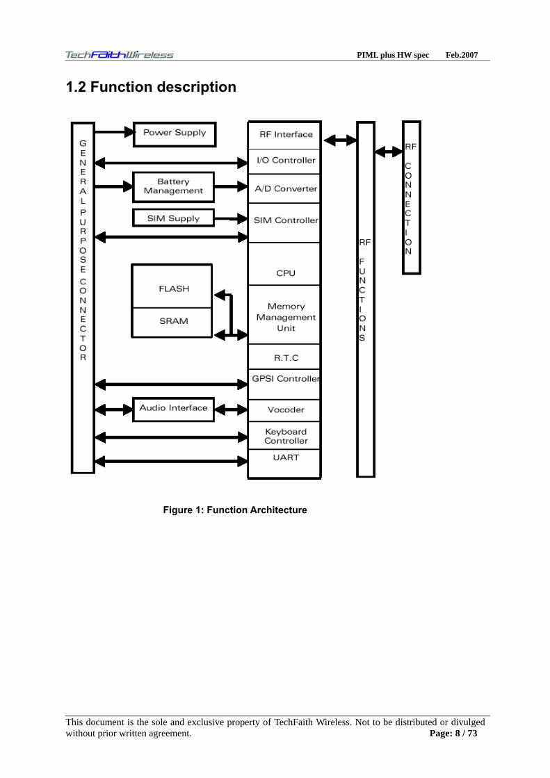
1.2 Function description
Figure 1: Function Architecture
This document is the sole and exclusive property of TechFaith Wireless. Not to be distributed or divulged without prior written agreement. Page: 8 / 73

PIML plus HW spec Feb.2007
1.2.1 RF functionalities
The RF functionalities comply with the Phase II recommendation. The frequencies are : · EGSM 900
TX: 880 to 915 MHz RX: 925 to 960 MHz · DCS1800
TX: 1710 to 1785 MHz RX: 1805 to 1880MHz · PCS1900
TX: 1850 to 1910 MHz RX: 1930 to 1990MHz
The RF part is based on a specific tri-band chip including: · Low-IF Receiver · Dual RF synthesizer · Digital IF to Baseband Converter · Offset PLL transmitter
· Tri-band PA module
1.2.2 Baseband functionalities
The digital part of the TECHFAITH WIRELESS PIML PLUS module is composed of a PHILIPS-VLSI chip (ONE C GSM/GPRS Kernel). This chipset is using a 0,25 µm mixed technology CMOS, which allows massive integration as well as low current consumption.
1.3 Firmware
TECHFAITH WIRELESS PIML PLUS module is designed to be integrated into various types of applications such as handsets or vertical applications (telemetry, multimedia, etc). For vertical applications, the firmware offers a set of AT commands to control the module. With this standard software, some interfaces of the module are not available since they are dependent on the peripheral devices connected to the module. They are the LCD interface
This document is the sole and exclusive property of TechFaith Wireless. Not to be distributed or divulged without prior written agreement. Page: 9 / 73

PIML plus HW spec Feb.2007
and the I2C bus.
2 Interfaces
2.1 General Purpose Connector (GPC)
A 60 pins connector1 is provided to interface the PIML PLUS module with a board containing either a LCD module, or a keyboard, or a SIM connector, or a battery connection... The interfaces available on the GPC are described in the next paragraphs.
· Please be aware that some of these interfaces can not be handled when using the PIML le driven by AT commands: LCD interface. PLUS moduThis symbol is used to indicate the interfaces not available with AT commands.
These functions have then to be managed externally i.e. using the main processor of the application. 1 The communication interface connector is a 60 pins connector with 0.5mm pitch from KYOCERA / AVX group with the following reference (see chapter connectors reference for further details): 14 5087 060 930 861. The matting connector has the following reference: 24 5087 060 X00 861. X = 2 or 9
2.2 Power supply
2.2.1 Power supply description
The power supply is one of the key issues in the design of a GSM terminal. Due to the burst emission in GSM / GPRS, the power supply must be able to deliver high current peaks in a
This document is the sole and exclusive property of TechFaith Wireless. Not to be distributed or divulged without prior written agreement. Page: 10 / 73

PIML plus HW spec Feb.2007
short time. During these peaks the ripple (Uripp) and the drop (Udrop) on the supply voltage must not exceed a certain limit.
· In transmission mode, a GSM/GPRS class 2 terminal emits (1Tx) 577µs radio bursts every 4.615ms.
In communication mode, a GPRS class 10 terminal emits 1154µs radio bursts every 4.615ms. VBATT is used to supply the RF part and the base band part. Notes : VBATT : supplies directly the RF components with 3.6 V. It is essential to minimize the voltage ripple at this connection in order to avoid any phase error. The RF Power Amplifier current (2.0A peak in GSM /GPRS mode) flows with a ratio of 1/8 of the time, around 577µs every 4.615ms for GSM /GPRS cl 2. The rising time is around 10µs.
The TECHFAITH WIRELESS PIML PLUS module shielding case is the grounding. The ground has to be connected on the motherboard through a complete layer on the PCB. Power Supply Voltage
This document is the sole and exclusive property of TechFaith Wireless. Not to be distributed or divulged without prior written agreement. Page: 11 / 73
PIML plus HW spec Feb.2007
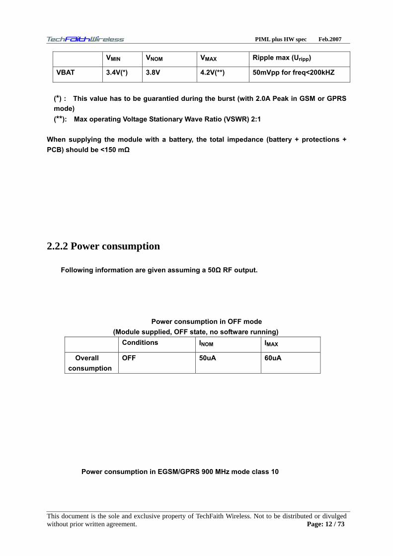
VMIN VNOM VMAX Ripple max (Uripp)
VBAT 3.4V(*) 3.8V 4.2V(**) 50mVpp for freq<200kHZ
(*) : This value has to be guarantied during the burst (with 2.0A Peak in GSM or GPRS mode) (**): Max operating Voltage Stationary Wave Ratio (VSWR) 2:1
When supplying the module with a battery, the total impedance (battery + protections + PCB) should be <150 mΩ
2.2.2 Power consumption
Following information are given assuming a 50Ω RF output.
Power consumption in OFF mode (Module supplied, OFF state, no software running)
Conditions INOM IMAX
Overall consumption
OFF 50uA 60uA
Power consumption in EGSM/GPRS 900 MHz mode class 10
This document is the sole and exclusive property of TechFaith Wireless. Not to be distributed or divulged without prior written agreement. Page: 12 / 73

PIML plus HW spec Feb.2007
Conditions INOM IMAX
VBATT+ During TX bursts @ PCL5* 1.7A peak 2.0A peak
VBATT+ During RX bursts 75mA peak 80mA peak
VBATT+ Average 1RX/1TX@PCL5* 270mA 320mA
VBATT+ Average 1RX/1TX@PCL8* 180mA 200mA
VBATT+ Average GPRS Cl 10 (3Rx/2Tx) @Pcl5
540mA 640mA
VBATT+ Average GPRS Cl 10(3Rx/2Tx) @Pcl8
360mA
400mA
VBATT+ Average Idle mode 2.2mA 3mA
(*) : PCL : Power Control Level. PCL 5: 2W emission requested (Max power)
PCL 8: 0.5W emission requested
Power consumption in GSM/GPRS 1800 MHz mode class 10 Conditions INOM IMAX
VBATT+ During TX bursts @ PCL0* 1.3A peak 1.7A peak
VBATT+ During RX bursts 75mA peak 80mA peak
VBATT+ Average 1RX/1TX@PCL0* 240mA 270mA
VBATT+ Average 1RX/1TX@PCL3* 150mA 180mA
VBATT+ Average GPRS Cl 10 (3Rx/2Tx) @PCL0
480mA 540mA
VBATT+ Average GPRS Cl 10 (3Rx/2Tx) @Pcl3
300mA
360mA
VBATT+ Average Idle mode 2mA 3mA
(*) : PCL : Power Control Level. PCL0 = 1W typ. PCL3 = 0.25W typ.
Power consumption in GSM/GPRS 1900 MHz mode class 10 Conditions INOM IMAX
VBATT+ During TX bursts @ PCL0* 1.3A peak 1.7A peak
VBATT+ During RX bursts 75mA peak 80mA peak
VBATT+ Average 1RX/1TX@PCL0* 240mA 270mA
This document is the sole and exclusive property of TechFaith Wireless. Not to be distributed or divulged without prior written agreement. Page: 13 / 73
PIML plus HW spec Feb.2007
VBATT+ Average 1RX/1TX@PCL3* 150mA 180mA
VBATT+ Average GPRS Cl 10 (3Rx/2Tx) @PCL0
480mA 540mA
VBATT+ Average GPRS Cl 10 (3Rx/2Tx) @Pcl3
300mA
360mA
VBATT+ Average Idle mode 2mA 3mA
(*) : PCL : Power Control Level. PCL0 = 1W typ. PCL3 = 0.25W typ.
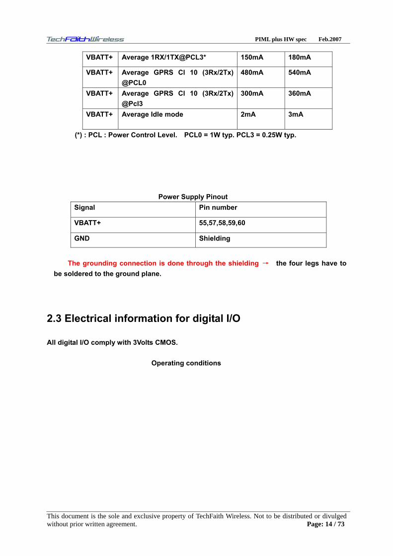
Power Supply Pinout Signal Pin number
VBATT+ 55,57,58,59,60
GND Shielding
The grounding connection is done through the shielding → the four legs have to
be soldered to the ground plane.
2.3 Electrical information for digital I/O
All digital I/O comply with 3Volts CMOS.
Operating conditions
This document is the sole and exclusive property of TechFaith Wireless. Not to be distributed or divulged without prior written agreement. Page: 14 / 73
PIML plus HW spec Feb.2007
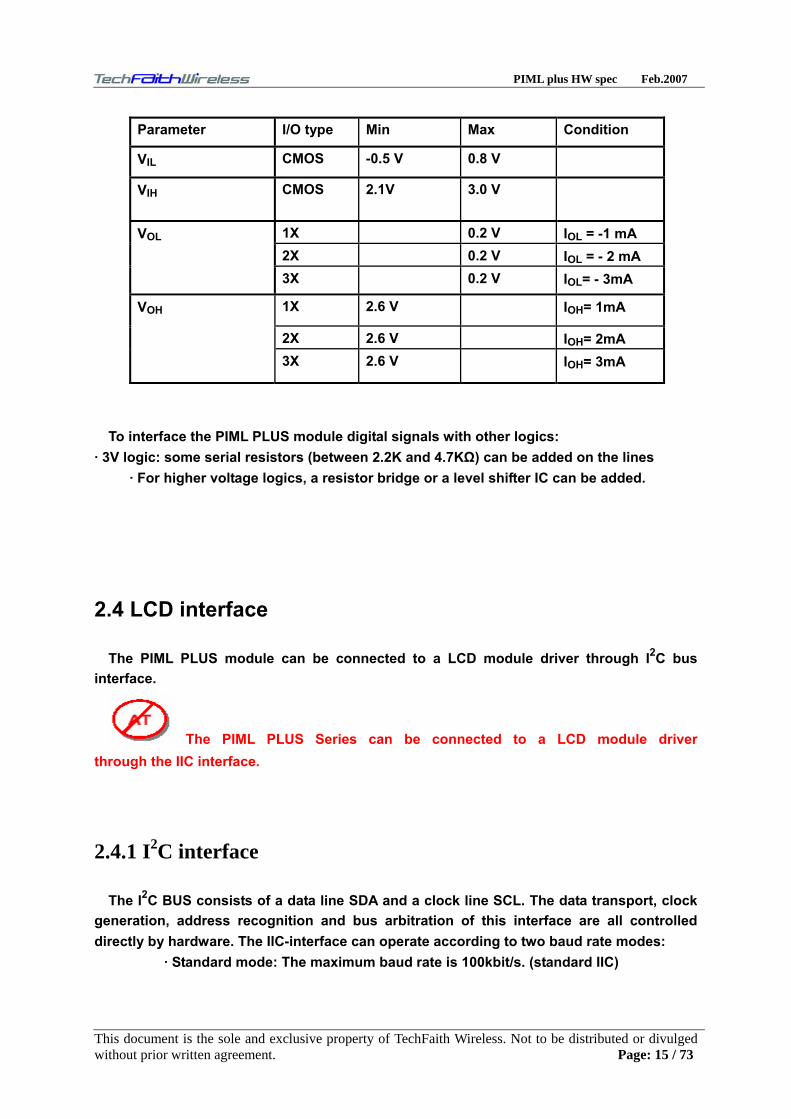
Parameter I/O type Min Max Condition
VIL CMOS -0.5 V 0.8 V
VIH CMOS 2.1V 3.0 V
1X 0.2 V IOL = -1 mA 2X 0.2 V IOL = - 2 mA
VOL
3X 0.2 V IOL= - 3mA
1X 2.6 V IOH= 1mA
2X 2.6 V IOH= 2mA
VOH
3X 2.6 V IOH= 3mA
To interface the PIML PLUS module digital signals with other logics: · 3V logic: some serial resistors (between 2.2K and 4.7KΩ) can be added on the lines · For higher voltage logics, a resistor bridge or a level shifter IC can be added.
2.4 LCD interface
The PIML PLUS module can be connected to a LCD module driver through I2C bus interface.
The PIML PLUS Series can be connected to a LCD module driver through the IIC interface.
2.4.1 I2C interface
The I2C BUS consists of a data line SDA and a clock line SCL. The data transport, clock generation, address recognition and bus arbitration of this interface are all controlled directly by hardware. The IIC-interface can operate according to two baud rate modes: · Standard mode: The maximum baud rate is 100kbit/s. (standard IIC)
This document is the sole and exclusive property of TechFaith Wireless. Not to be distributed or divulged without prior written agreement. Page: 15 / 73

PIML plus HW spec Feb.2007
· Fast mode: The maximum baud rate is 400kbit/s. (Fast IIC) Note: Devices with a 0 to 100kbit/s IIC-interface cannot be incorporated in the IIC-bus
system, if the 400kbit/s fast mode is chosen. Unpredictable states of these devices would occur, since they cannot follow the higher transfer rate.
Pin description Signal Pin number I/O I/O TYPE Description
SCL
10
O
1X
Serial clock
SDA 8 I/O CMOS /1X Data
2.5 Keyboard interface
Warning: This interface is not FULLY available with AT commands: An AT commands allows getting the input key code (see +CMER command description). This code has then to be processed by the application.
This interface provides 8 connections: 4 rows (ROW0 to ROW3) and 4 columns (COL0 to COL3). The scanning is a digital one , and the debouching is done in the TECHFAITH WIRELESS PIML PLUS Series. No discrete components like R, C (Resistor, Capacitor) are needed.
Pin description Signal Pin number I/O I/O type Description
ROW0 13 I/O COMS/1X Row scan
ROW1 15 I/O COMS/1X Row scan ROW2 17 I/O COMS/1X Row scan
ROW3 19 I/O COMS/1X Row scan
COL0 23 I/O COMS/1X Column scan
This document is the sole and exclusive property of TechFaith Wireless. Not to be distributed or divulged without prior written agreement. Page: 16 / 73
PIML plus HW spec Feb.2007
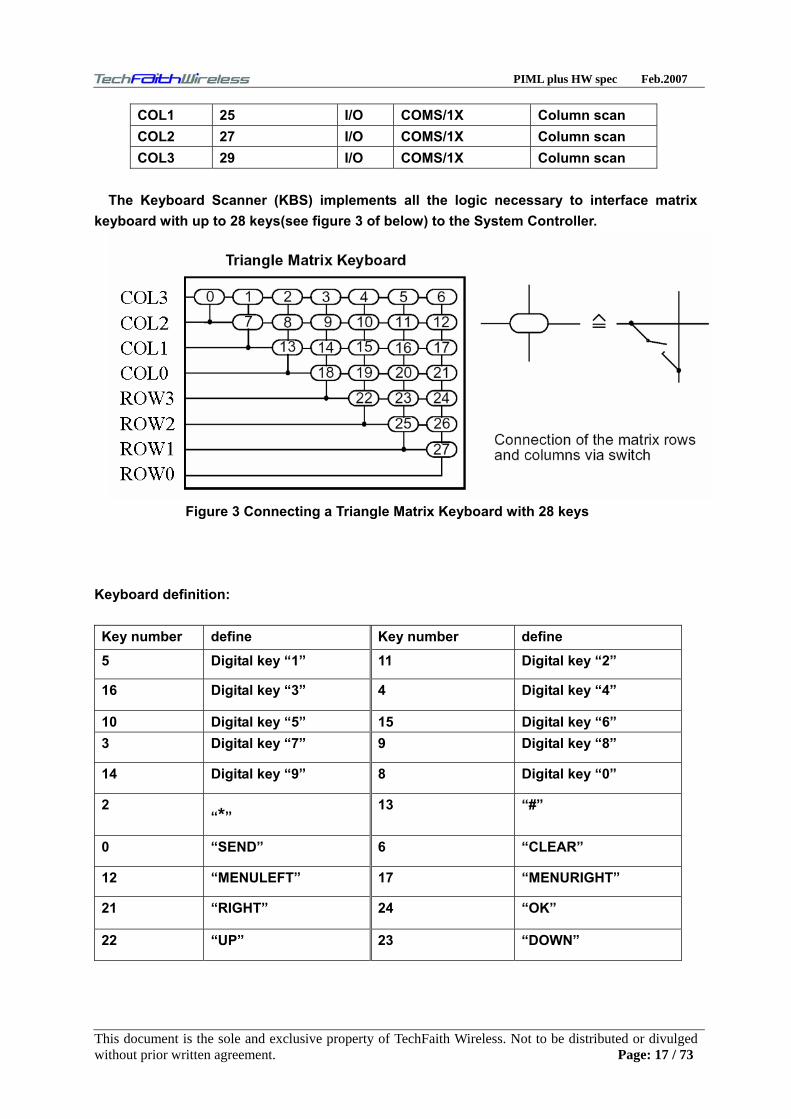
COL1 25 I/O COMS/1X Column scan COL2 27 I/O COMS/1X Column scan COL3 29 I/O COMS/1X Column scan
The Keyboard Scanner (KBS) implements all the logic necessary to interface matrix
keyboard with up to 28 keys(see figure 3 of below) to the System Controller.
Figure 3 Connecting a Triangle Matrix Keyboard with 28 keys
Keyboard definition: Key number define Key number define 5 Digital key “1” 11 Digital key “2”
16 Digital key “3” 4 Digital key “4”
10 Digital key “5” 15 Digital key “6” 3 Digital key “7” 9 Digital key “8”
14 Digital key “9” 8 Digital key “0”
2 “*”
13 “#”
0 “SEND” 6 “CLEAR”
12 “MENULEFT” 17 “MENURIGHT”
21 “RIGHT” 24 “OK”
22 “UP” 23 “DOWN”
This document is the sole and exclusive property of TechFaith Wireless. Not to be distributed or divulged without prior written agreement. Page: 17 / 73

PIML plus HW spec Feb.2007
25 “LEFT” 19 “SIDEDOWN”
18 “SIDEUP”
Additional comments on Keyboard: The exemplify keys are defined, that keys that unmentioned in table, can be defined anon.
2.6 Main Serial link (UART1)
A flexible 6 wires serial interface is available complying with V24 protocol signaling but not with V28 (electrical interface) due to a 2.8 Volts interface.
The signals are TX data (CT103/TX), RX data (CT104/RX), Request To Send (CT105/RTS),
Clear To Send (CT106/CTS), Data Terminal Ready (CT108-2/DTR) and Data Set Ready (CT107/DSR).
The set of RS232 signals can be required for GSM DATA services application and is
generated by the general purpose I/O provided by the Q24x6 series. The 2 additional signals are Data Carrier Detect (CT109/DCD) and Ring Indicator (CT125/RI).
The signals are TX data (TXD0), Rx data (RXD0), Request To Send (RTS0), Clear To Send (CTS0), Data Terminal Ready (DTR0) and Data Set Ready (DSR0).
Pin description
Signal Pin number
I/O I/O TYPE Description
CT103/TXD1 39 I CMOS Transmit serial data
CT104/RXD1 32 O 1X Receive serial data
CT105/RTS1 30 I CMOS Ready to Send
CT106/CTS1 37 O 1X Clear to send
CT107/DSR1 36 O 1X Data set ready
CT108/DTR1 34 I CMOS Data terminal ready
CT109/DCD1 51 O CMOS/2x Data carrier detect
CT125/RI1 54 O CMOS/2x Ring indicator
This document is the sole and exclusive property of TechFaith Wireless. Not to be distributed or divulged without prior written agreement. Page: 18 / 73
PIML plus HW spec Feb.2007
GND Shielding legs
Ground
The rising time and falling time of the reception signals (mainly CT103) have to be less than 200 ns. The PIML PLUS module has been designed to be operated using all the serial interface signals. In particular, it is necessary to use RTS1 and CTS1 for hardware flow control in order to avoid data corruption during transmission.
2.6.1 Typical implementation with a RS232 Terminal
The figure below shows a typical implementation when the PIML PLUS Module is
connected to a RS232 Terminal.
This document is the sole and exclusive property of TechFaith Wireless. Not to be distributed or divulged without prior written agreement. Page: 19 / 73

PIML plus HW spec Feb.2007
2.6.2 Typical implementation with a microprocessor
The figure below shows a typical implementation when the PIML PLUS Module is connected to a host microprocessor which is 2.8 V tolerant on the serial port signals.
This document is the sole and exclusive property of TechFaith Wireless. Not to be distributed or divulged without prior written agreement. Page: 20 / 73

PIML plus HW spec Feb.2007
2.7 SIM interface
2.7.1 General Description
5 signals exist: · SIMVCC: SIM power supply. · SIMRST: reset. · SIMCLK: clock.
· SIMDATA: I/O port. · SIMPRES: SIM Card detection.
The SIM Interface (SIMI) controls the activation- and deactivation sequences of the SIM card and provides the driver circuits for the SIM card. The protocol handling is not part of this module.
The SIM Interface controls a 3V SIM. This interface complies with the ETSI GSM 11.11, GSM 11.12 and GSM 11.18 requirements. Note that these specifications refer to ISO7813-3 for the “Operation Procedures” that define the activation and deactivation sequences.
It is recommendations concerning SIM functions. It is recommended to add Transient Voltage Suppressor diodes on the signal connected to the SIM socket in order to prevent
This document is the sole and exclusive property of TechFaith Wireless. Not to be distributed or divulged without prior written agreement. Page: 21 / 73

PIML plus HW spec Feb.2007
any Electrostatic Discharge. TVS diodes with low capacitance (less than 10pF) have to be connected on SIMCLK and SIMDATA to avoid any disturbance of the rising and falling edge. These types of diodes are mandatory for the Full Type Approval. They shall be placed as close as possible to the SIM socket.
The following references can be used: Pin description
Signal Pin number I/O I/O type Description
SIMCLK 3 O 2X SIM Clock
SIMRST 5 O 2X SIM reset
SIMDATA 7 I/O CMOS/3X SIM DATA
SIMVCC 9 O Supply SIM Power supply
SIMPRES O 1X SIM card detect
Electrical Characteristics
Parameter Conditions Min Typ Max Unit
SIMDATA VIH IIH = ±20uA 0.7 x SIM_VCC V
SIMDATA VIL IIL = 1mA 0.3xSIM_VCC V
SIMRST SIMDATA SIMCLK VOH
Source current =20uA
SIM_VCC-0.1V
V
SIMRST SIMDATA SIMCLK VOL
Sink current = 200uA
0.1
V
SIMVCC Output Voltage
ISIM_VCC<=6mA
2.70
2.80
2.85
V
SIMCLK Rise/Fall Time
Loaded with 30pF
50
nS
This document is the sole and exclusive property of TechFaith Wireless. Not to be distributed or divulged without prior written agreement. Page: 22 / 73
PIML plus HW spec Feb.2007
SIMRST, SIMDATA Rise/Fall Time
Loaded with 30pF
1 uS
SIMCLK Frequency
Loaded with 30pF
3.25 MHz
(*) : given for the 3V interface. Notes:
When not used SIMPRES cannot be connected. When used, a low to high transition means that the SIM card is inserted and a high to low transition means that the SIM card is removed.
2.7.2 SIM socket connection
SIM socket pin description
Signal Pin number Description CLK 1 SIMCLK I/O 2 SIMDATA REST 3 SIMRST VCC 4 SIMVCC GND 5 GND
Typical implementation:
This document is the sole and exclusive property of TechFaith Wireless. Not to be distributed or divulged without prior written agreement. Page: 23 / 73

PIML plus HW spec Feb.2007
SIM socket
2.8 General Purpose Input/Output
The TECHFAITH WIRELESS PIML PLUS module provides 7 General Purpose I/O, 1 General Purpose Output. They are used to control any external device such as a LCD or a Keyboard backlight. Pin description
Signal Pin number I/O Description Multiplexed with GPIO0 24 I/O General Purpose I/O GPIO2 53 I/O General Purpose I/O GPO0 26 O General Purpose output GPO1 22 O General Purpose output GPO2 20 O General Purpose output GPO3 28 O General Purpose output
GPO4 52 O General Purpose output GPI0 18 I General Purpose input GPI1 35 I General Purpose input
The following GPIOs are not available (reserved) in case of module running with the AT commands firm ware:
Signal Pin number I/O Description Multiplexed with
GPO4 52 O General Purpose output FLASH LED (*)
This document is the sole and exclusive property of TechFaith Wireless. Not to be distributed or divulged without prior written agreement. Page: 24 / 73
PIML plus HW spec Feb.2007
GPO3 28 O General Purpose output GPI0 18 I General Purpose input GPI1 35 I General Purpose output GPO0 26 O General Purpose output
GPO1 22 O General Purpose output GPO2 20 O General Purpose output GPO3 28 O General Purpose output
(*)The FLASH LED signal can be used to drive a LED through an open-collector transistor according to the module activity status. LED status PIML PLUS module status
OFF Module OFF
Permanent Module switch ON, not registered on the network ON
Flash LED on for 1s, off for 1s
Module switch on, registered on the network, communication in progress
2.9 Analog to Digital Converter
The TECHFAITH WIRELESS PIML PLUS module provides an Analog to Digital Converter (ADC) input. This ADC section is specified for voltage and temperature measurements. Its input channel required for T and V measurement, as well as battery type recognition. This converter is a 12 bits one, ranging from 0 to 2.8V. Pin description
Signal Pin number I/O I/O type Description
AUXV0 33 I Analog A/D converter
Electrical characteristics
Parameter Min Max Unit
Resolution 12 bits
Input signal range 0 2.8 V ADC Reference Accuracy 0.22 0.25 %
This document is the sole and exclusive property of TechFaith Wireless. Not to be distributed or divulged without prior written agreement. Page: 25 / 73

PIML plus HW spec Feb.2007
PIML900-1800 module also monitors the temperature of the battery through the AUXV0 pin that has to be connected to a temperature sensor inside the battery (a NTC resistor for instance).
2.9.1 How to define R1 and C1
How to choose R1 R1 has to be chosen to have a full range of BAT-TEMP (from 0V to 2.8V) when the CTN value changes from the minimum to the maximum temperature How to choose C1 C1 has to be chosen to have a RC filter with a time constant lower than 2ms. Calculation examples CTN(25) = 47K CTN(55) = 10K CTN(-10) = 300K CTN(-10) x VCC = ( CTN(-10) + R1 ) x BAT-TEMP (full range) R1= 47K BAT-TEMP(-20) = 2.42V BAT-TEMP(55) = 0.49V R(-20) = R1//CTN(-10) = 40K R(+55) =8K With C=10nF: RC(-20) = 400us RC(+55) = 80us
This document is the sole and exclusive property of TechFaith Wireless. Not to be distributed or divulged without prior written agreement. Page: 26 / 73

PIML plus HW spec Feb.2007
2.10 Audio interface
The TECHFAITH WIRELESS PIML PLUS module’s audio interface supports two different microphone inputs (MIC1、MIC2)and two different speaker outputs (SPK1、SPK2). The MIC2 inputs already include the biasing for an electret microphone allowing an easy connection to a handset. The interface also includes an echo cancellation feature, which allows hands free function.
2.10.1 Main audio interface
Main audio interface consists of MIC2 (MIC2P, MIC2N) and SPK2 (SPK2P, SPK2N). The connection can be either differential or single-ended, but using a differential connection in order to reject common mode noise and TDMA noise is strongly recommended. When using a single-ended connection, be sure to have a very good ground plane, a very good filtering as well as shielding in order to avoid any disturbance on the audio path.
2.10.1.1 Main Microphone Inputs (MIC2)
The MIC2 already include the convenient biasing for an electret microphone . This electret microphone can be directly connected on these inputs. These inputs are the standard ones used for an external headset or a hands free kit Typical implementation (differential connection):
MIC2 input connect
This document is the sole and exclusive property of TechFaith Wireless. Not to be distributed or divulged without prior written agreement. Page: 27 / 73
PIML plus HW spec Feb.2007
C1 = C2= C3 = 39pF R1 = R2 = 0 ohm C1 has to be the nearest possible to the microphone. Microphone manufacturers provide this capacitor directly soldered on the microphone. R1, R2, C2 and C3 have to be put near the PIML PLUS Series connector and can be removed according to their environment (ground plane, shielding, etc). The best way is to plan all the components and to remove those that are not necessary to filter out the TDMA noise on the audio path. Recommended characteristics for the microphone:
2V 0.5mA 2.2 KΩ Sensitivity -40 to –50dB SNR > 60dB Frequency response compatible with the GSM specifications
Pin description Signal Pin number I/O I/O type Description MIC2P 46 I Analog Microphone 2 positive input
MIC2N 48 I Analog Microphone 2 negative input
2.10.1.2 Main speaker outputs (SPK2)
The main speaker outputs SPK2 includes SPK2P and SPK2N. Typical implementation (differential connect):
This document is the sole and exclusive property of TechFaith Wireless. Not to be distributed or divulged without prior written agreement. Page: 28 / 73

PIML plus HW spec Feb.2007
SPK2 connector
C1=C2=C3=56pF; L1=L2=120nH Recommended characteristics for the speaker: · Type : 50mW, electro-magnetic · Impedance : 32 Ohm · Sensitivity:110 dB SPL min.
· Frequency response compatible with the GSM specifications Pin description
Signal Pin number I/O I/O type Description
SPK2P 45 O Analog SPK 2 positive output
SPK2N 47 O Analog SPK 2 negative output
2.10.2 Auxiliary audio interface
The auxiliary audio interface consists of MIC1 (MIC1P, MIC1N) and SPK1 (SPK1P, SPK1N). Pin description
Signal Pin number I/O I/O type Description
MIC1P 42 I Analog MIC1 positive input
MIC1N 44 I Analog MIC1 negative input
SPK1P 41 O Analog SPK 1 positive output
This document is the sole and exclusive property of TechFaith Wireless. Not to be distributed or divulged without prior written agreement. Page: 29 / 73

PIML plus HW spec Feb.2007
SPK1N 43 O Analog SPK 1 negative output
2.10.2.1 Auxiliary Microphone Inputs (MIC1)
The MIC1 inputs are differential and do not include internal bias. To use these inputs with an electret microphone, bias has to be generated outside the PIML PLUS module according to the characteristic of this electret microphone. These inputs are the standard ones used for an external headset or a hands free kit. AC coupling is already embedded in the module.
2.10.2.1.1 Differential connection
Impedance of the microphone input in differential mode : Module ON : Rin = 10KΩ +/-10% Module OFF : Rin >1MΩ +/-10% Typical implementation:
This document is the sole and exclusive property of TechFaith Wireless. Not to be distributed or divulged without prior written agreement. Page: 30 / 73

PIML plus HW spec Feb.2007
Figure 4 : MIC1 inputs (differential connection) R1 = R4 = from 100 to 330Ω R2 = R3 = usually between 1KΩand 3.3K Ω as per the microphone characteristics C1 = 10pF to 33pF C2 = C3 = C4 = 47pF to 100pF C5 = 47uF L1 = L2 = 100nH R1 and R4 are used as a voltage supply filter with C5. C1 has to be the nearest possible to the microphone. Microphone manufacturers
provide this capacitor directly soldered on the microphone. C2 has to be very close to the PIML PLUS connector.
L1, L2, C3 and C4 have to be put near the PIML PLUS connector and can be removed according to their environment (ground plane, shielding ...etc). The best way is to plan all the components and to remove those which are not necessary to filter out the TDMA noise on the audio path.
This document is the sole and exclusive property of TechFaith Wireless. Not to be distributed or divulged without prior written agreement. Page: 31 / 73
PIML plus HW spec Feb.2007
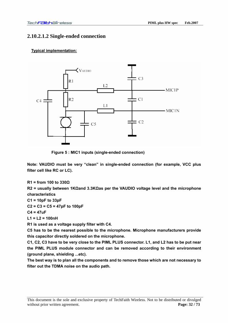
2.10.2.1.2 Single-ended connection
Typical implementation:
Figure 5 : MIC1 inputs (single-ended connection) Note: VAUDIO must be very “clean” in single-ended connection (for example, VCC plus filter cell like RC or LC). R1 = from 100 to 330Ω R2 = usually between 1KΩand 3.3KΩas per the VAUDIO voltage level and the microphone characteristics C1 = 10pF to 33pF C2 = C3 = C5 = 47pF to 100pF C4 = 47uF L1 = L2 = 100nH R1 is used as a voltage supply filter with C4. C5 has to be the nearest possible to the microphone. Microphone manufacturers provide this capacitor directly soldered on the microphone. C1, C2, C3 have to be very close to the PIML PLUS connector. L1, and L2 has to be put near the PIML PLUS module connector and can be removed according to their environment (ground plane, shielding ...etc). The best way is to plan all the components and to remove those which are not necessary to filter out the TDMA noise on the audio path.
This document is the sole and exclusive property of TechFaith Wireless. Not to be distributed or divulged without prior written agreement. Page: 32 / 73
PIML plus HW spec Feb.2007
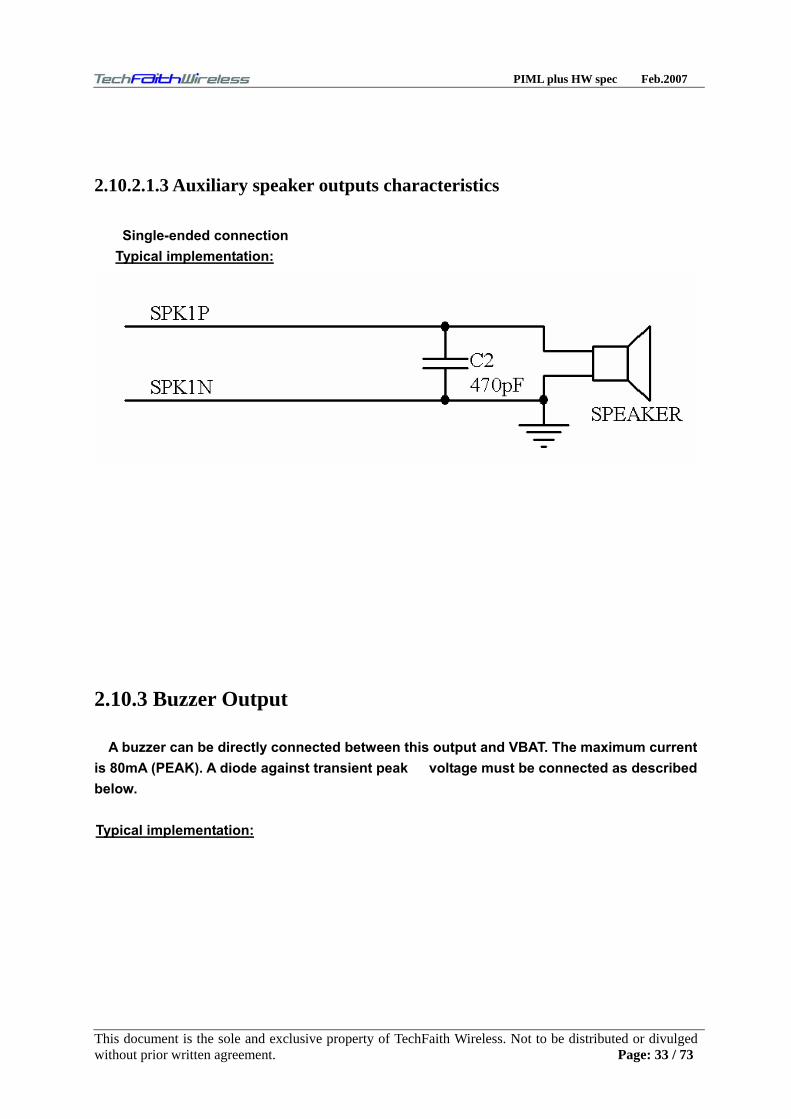
2.10.2.1.3 Auxiliary speaker outputs characteristics
Single-ended connection Typical implementation:
2.10.3 Buzzer Output
A buzzer can be directly connected between this output and VBAT. The maximum current is 80mA (PEAK). A diode against transient peak voltage must be connected as described below.
Typical implementation:
This document is the sole and exclusive property of TechFaith Wireless. Not to be distributed or divulged without prior written agreement. Page: 33 / 73

PIML plus HW spec Feb.2007
C1=0.1uF
Recommended characteristics for the buzzer: · Type: Electromagnetic · Impedance : 7 to 30 ohm · Sensitivity : 90 dB SPL min @ 10 cm
Pin description Signal Pin number I/O I/O type Description BUZ 49 O Analog BUZ positive output
2.11 Battery charging interface
The PIML PLUS module supports one battery charging circuit for Li-Ion batteries. This circuit uses an interface, which consists of a current source inputs (CHG_IN) where the constant current has to flow in order to charge the battery. This current value depends on the battery capacity. It is recommended to provide a current equal to the value of the capacity plus 50mA. For a 550mA battery the current will be 600mA. The maximum current is 800mA. A specific AT command (+WCBM), available from 4.3 level, allows to manage the charge battery (start and stop the charge, enable or disable unsolicited Battery Charge Indications and set the battery charge parameters). The PIML PLUS Series module monitors the battery voltage to detect the end of the charge.
This document is the sole and exclusive property of TechFaith Wireless. Not to be distributed or divulged without prior written agreement. Page: 34 / 73

PIML plus HW spec Feb.2007
Pin description
Signal Pin number I/O I/O type description
CHG_IN 1,2,4 I/O Supply Current source input
Electrical Characteristics
Parameter Min Max Type Unit
CHARGE IN voltage (for I=Imax)
+VBAT max+0.7V 5.5 V
CHARGE IN Current 800 mA
* To be parameterized as per battery manufacturer
2.11.1 Li-ion charging procedure
Charge the Li-ion battery during this procedure the voltage of the battery is accurately monitored. The Li-ion charging involves two phases. During the first phase, the battery is charged with a constant current until its voltage reaches 4.1V*. During the second phase the constant current is pulsed by the module. The width and the frequency of the pulse change during this phase in order to ensure a safety charge. The battery is considered as fully charged when, after a pulse, the voltage remains at a 4.1V* during more than 10s. The Li-ion battery must have an included safety circuit to avoid any discharge or overcharge. The manufacturer inside the battery delivers this circuit pack. The impedance of this safety circuit has to be the lowest possible in order to reduce the drop-out of the voltage. This drop-out is due to the RF Power Amplifier current (up to 2.0A). A maximum of 150mΩ is required.
This document is the sole and exclusive property of TechFaith Wireless. Not to be distributed or divulged without prior written agreement. Page: 35 / 73

PIML plus HW spec Feb.2007
(*): To be parameterized as per battery manufacturer
2.12 ON / OFF
This input is used to switch ON or OFF the PIML PLUS Series module. A low level signal, that more than 14ms, has to be provided on the pin ON/~OFF to switch ON the module. The level of the voltage of this signal has to be maintained between 0V and 0.3v. To be able to switch OFF the module, the pin ON/OFF has to be keeping low level signal during a minimum of 1000ms. Through the firmware, the module can be switched off (using the CPOF command).
Pin description
Signal Pin number I/O I/O type Description
ON/OFF 6 I CMOS Module Power ON/OFF
Operating conditions Parameter I/O Type Min Max Unit
VIL 0 0.3 V
VIH 2.4 VBATT V
2.12.1 Operating sequences
2.12.1.1 Power ON
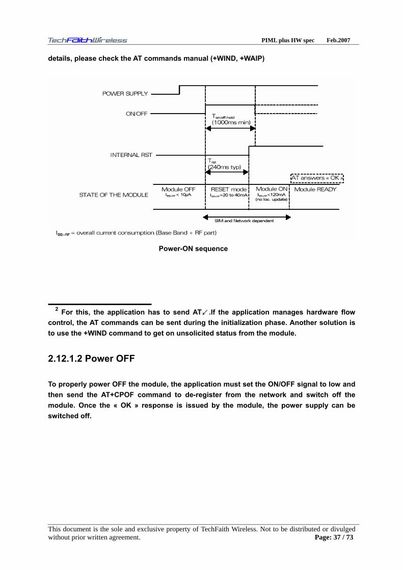
Once the module supplied, the application must set the ON/OFF signal to high to start the module power ON sequence. The ON/OFF signal must be hold for 1000ms minimum. After this time, an internal mechanism keeps it on hold. During the power ON sequence, an internal reset is automatically performed by the module for 240ms (typical). During this phase, any external reset should be avoided. Once the initialization is complete (timing is SIM and network dependent) the AT interface answers 《OK》to the application2. For further
This document is the sole and exclusive property of TechFaith Wireless. Not to be distributed or divulged without prior written agreement. Page: 36 / 73
PIML plus HW spec Feb.2007
details, please check the AT commands manual (+WIND, +WAIP)
Power-ON sequence 2 For this, the application has to send AT.If the application manages hardware flow control, the AT commands can be sent during the initialization phase. Another solution is to use the +WIND command to get on unsolicited status from the module.
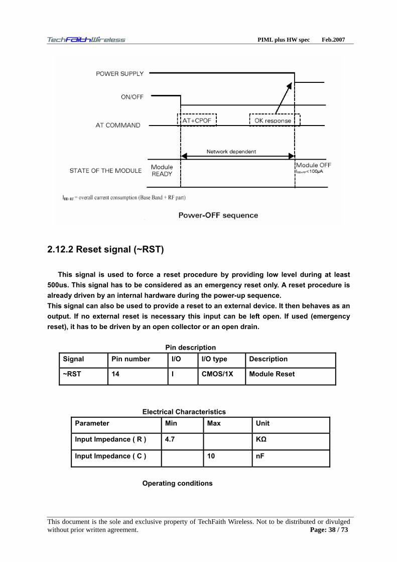
2.12.1.2 Power OFF
To properly power OFF the module, the application must set the ON/OFF signal to low and then send the AT+CPOF command to de-register from the network and switch off the module. Once the « OK » response is issued by the module, the power supply can be switched off.
This document is the sole and exclusive property of TechFaith Wireless. Not to be distributed or divulged without prior written agreement. Page: 37 / 73
PIML plus HW spec Feb.2007
2.12.2 Reset signal (~RST)
This signal is used to force a reset procedure by providing low level during at least 500us. This signal has to be considered as an emergency reset only. A reset procedure is already driven by an internal hardware during the power-up sequence. This signal can also be used to provide a reset to an external device. It then behaves as an output. If no external reset is necessary this input can be left open. If used (emergency reset), it has to be driven by an open collector or an open drain.
Pin description Signal Pin number I/O I/O type Description
~RST 14 I CMOS/1X Module Reset
Electrical Characteristics
Parameter Min Max Unit
Input Impedance ( R ) 4.7 KΩ
Input Impedance ( C ) 10 nF
Operating conditions
This document is the sole and exclusive property of TechFaith Wireless. Not to be distributed or divulged without prior written agreement. Page: 38 / 73

PIML plus HW spec Feb.2007
Parameter Min Max Conditions
*VT- 1.1V 1.2V *VT+ 1.7V 1.9V VOL 0.4V IOL=-50uA
VOH 2.0V IOH=50uA *VT-, VT+: hysteresis level Additional comments on RESET: The RESET process is activated either by the external ~RST signal or by an internal signal (coming from a RESET generator). This automatic reset is activated at Power-up. The module remains in reset mode as long as the RST signal is held low. This signal should be used only for “emergency” resets. A software reset will be preferred to a HW reset.
2.12.2.1 Reset sequence
To activate the “emergency” reset sequence, the ~RST signal has to be set to low for 500us minimum. As soon as the reset is complete, the AT Interface answers “OK” to the application3. 3 For this, the application has to send AT . If the application manages hardware flow control, the AT commands can be sent during the initialization phase. Another solution is to use the +WIND command to get an unsolicited status from the module.
This document is the sole and exclusive property of TechFaith Wireless. Not to be distributed or divulged without prior written agreement. Page: 39 / 73

PIML plus HW spec Feb.2007
2.13 External Interrupt (~INTR)
The PIML PLUS Series provides an external interrupt input (not managed in the standard AT commands firmware). This input is very sensitive and an interrupt is activated on high to low edge. If this signal is not used it can be left open. If used this input has to be driven by an open collector or an open drain. This input is used for instance to power OFF automatically the module. Pin description
Signal Pin number I/O I/O type Description ~INTR 16 I CMOS Active low
2.14 VCC output
This output can be used to power some external functions. VCC has to be used as a digital power supply. This power supply is available programmed.
Pin description Signal Pin number I/O I/O type Description
VCC 40 O Supply Digital supply
Operating conditions
This document is the sole and exclusive property of TechFaith Wireless. Not to be distributed or divulged without prior written agreement. Page: 40 / 73
PIML plus HW spec Feb.2007
Output voltage (V) Output current(mA) Min Max Max
VCC 1.35 3.45 150
2.15 VCC_RTC (REAL TIME CLOCK SUPPLY)
2.15.1 Interface description
This pin is used as a back-up power supply for the internal Real Time Clock. The RTC is supported by the module when powered on but a back-up power supply is needed to save date and hour when the module is switched off. If the RTC is not used this pin can be left open. Pin Description
Signal Pin number I/O I/O type Description
VCC_RTC 56 I/O Supply RTC BACK-UP SUPPLY
Operating conditions
Parameter Condition Min Max Unit
Input voltage -0.5 6.5 V
Input Current VBACK < VBAT - 0.5V 1 uA
Output voltage 2.4 3.09 V
Output current 2 mA
This document is the sole and exclusive property of TechFaith Wireless. Not to be distributed or divulged without prior written agreement. Page: 41 / 73
PIML plus HW spec Feb.2007
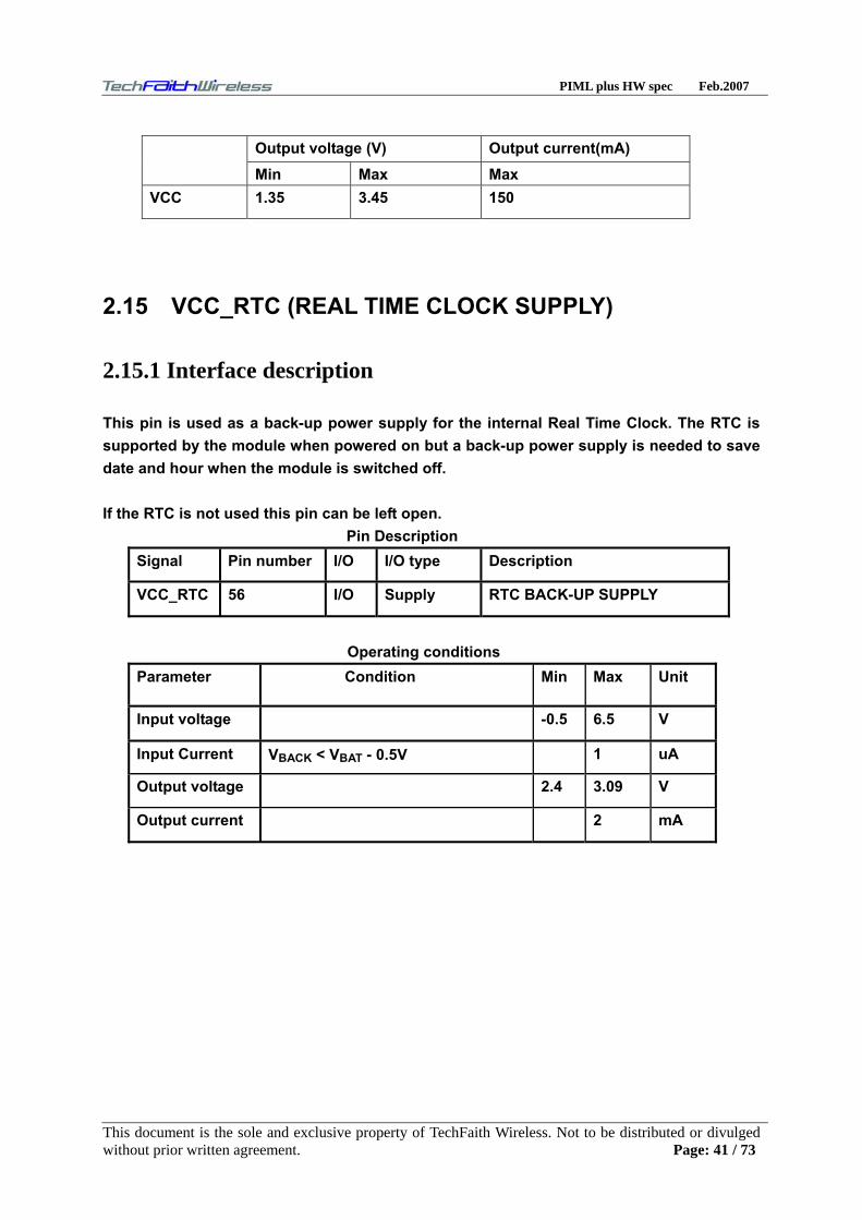
2.15.2 Typical implementation:
2.15.2.1 Capacitor
Estimated range with 470uF Capacitor : ~30 seconds.
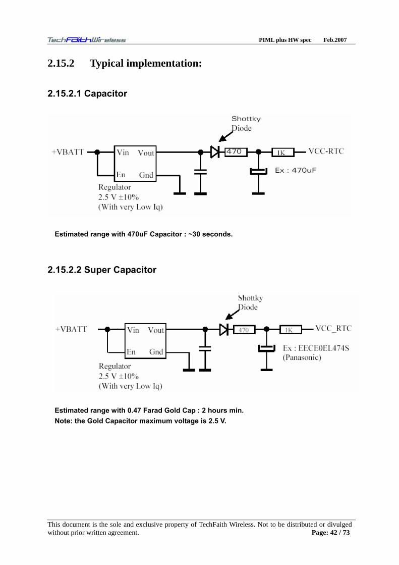
2.15.2.2 Super Capacitor
Estimated range with 0.47 Farad Gold Cap : 2 hours min. Note: the Gold Capacitor maximum voltage is 2.5 V.
This document is the sole and exclusive property of TechFaith Wireless. Not to be distributed or divulged without prior written agreement. Page: 42 / 73
PIML plus HW spec Feb.2007
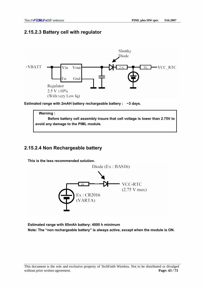
2.15.2.3 Battery cell with regulator
Estimated range with 2mAH battery rechargeable battery : ~3 days.
Warning : Before battery cell assembly insure that cell voltage is lower than 2.75V to
avoid any damage to the PIML module.
2.15.2.4 Non Rechargeable battery
This is the less recommended solution.
Estimated range with 85mAh battery: 4000 h minimum Note: The “non rechargeable battery” is always active, except when the module is ON.
This document is the sole and exclusive property of TechFaith Wireless. Not to be distributed or divulged without prior written agreement. Page: 43 / 73
PIML plus HW spec Feb.2007
2.16 RF interface
Three types of RF connection are available:
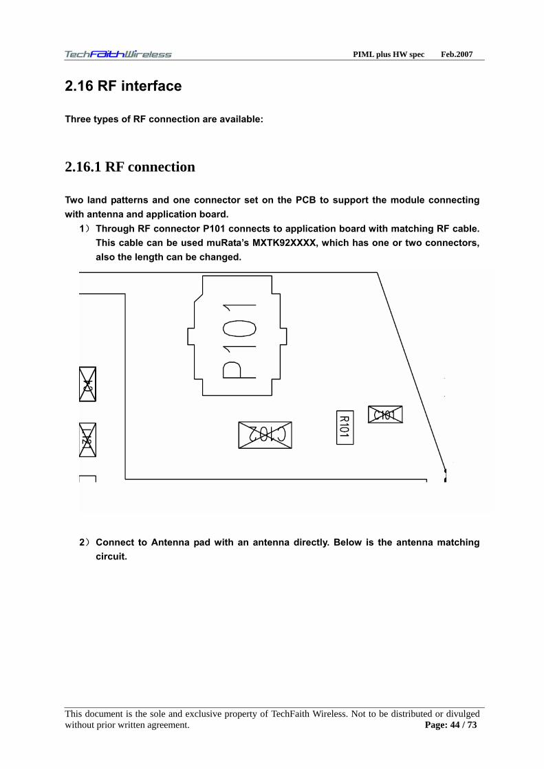
2.16.1 RF connection
Two land patterns and one connector set on the PCB to support the module connecting with antenna and application board.
1) Through RF connector P101 connects to application board with matching RF cable. This cable can be used muRata’s MXTK92XXXX, which has one or two connectors, also the length can be changed.
2) Connect to Antenna pad with an antenna directly. Below is the antenna matching
circuit.
This document is the sole and exclusive property of TechFaith Wireless. Not to be distributed or divulged without prior written agreement. Page: 44 / 73

PIML plus HW spec Feb.2007
3) Through soldering RF cable to other application board. Solder cable corn to solder pad and GND to GND pad.
Antenna pad
Solder pad
GND pad
This document is the sole and exclusive property of TechFaith Wireless. Not to be distributed or divulged without prior written agreement. Page: 45 / 73

PIML plus HW spec Feb.2007
Notes: · The antenna cable and connector should be chosen in order to minimize
losses in the frequency bands used for GSM 900MHz ,DCS1800MHz and PCS1900MHz.
· 0.5dB can be considered as a maximum value for insert loss between the module and an external connector.
2.16.2 RF performances
RF performances are compliant with the ETSI recommendation 05. The main parameters for Receiver are: ·EGSM/900 Sensitivity: < -102dBm Static & TUHigh ·DCS1800 Sensitivity: < -102dBm Static & TUHigh ·PCS1900 Sensitivity: < -102dBm Static & TUHigh ·Selectivity @ 200 kHz: > +9dBc ·Selectivity @ 400 kHz: > +41dBc ·Dynamic range: 63dB ·Co-channel rejection: >= 9dBc And for Transmitter: · Maximum output power (EGSM): 33dBm +/- 2 dB at ambient temperature · Maximum output power (DCS1800/PCS1900): 30dBm +/- 2 dB at ambient temperature · Minimum output power (EGSM): 5dBm +/- 5 dB at ambient temperature · Minimum output power (DCS1800/PCS1900): 0dBm +/- 5 dB at ambient temperature · H2 level: < -30dBm · H3 level: < -30dBm · Noise in 925 - 935 MHz: < -67dBm · Noise in 935 - 960 MHz: < -79dBm · Noise in 1930 - 1990 MHz (GSM1900 band): < -71dBm · Phase error at peak power: < 5 ° RMS · Frequency error: +/- 0.1 ppm max
2.16.3 Antenna specifications
The antenna must fulfill the following requirements: · Frequency bands: dual band E-GSM 900MHz – GSM 1800 MHz
EGSM 900 DCS 1800 PCS 1900
Frequency RX 925 to 960 MHz 1805 to 1880 MHz 1930 to 1990 MHz
This document is the sole and exclusive property of TechFaith Wireless. Not to be distributed or divulged without prior written agreement. Page: 46 / 73
PIML plus HW spec Feb.2007
Frequency TX 880 to 915 MHz 1710 to 1785 MHz 1850 to 1910 MHz
· Impedance: 50Ω
3 Technical specifications
3.1 Interface
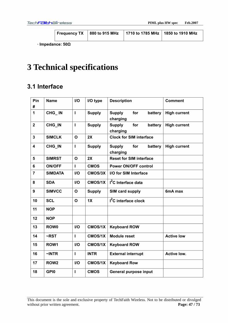
Pin #
Name I/O I/O type Description Comment
1 CHG_ IN I Supply Supply for battery charging
High current
2 CHG_IN I Supply Supply for battery charging
High current
3 SIMCLK O 2X Clock for SIM interface
4 CHG_IN I Supply Supply for battery charging
High current
5 SIMRST O 2X Reset for SIM interface
6 ON/OFF I CMOS Power ON/OFF control
7 SIMDATA I/O CMOS/3X I/O for SIM Interface
8 SDA I/O CMOS/1X I2C Interface data
9 SIMVCC O Supply SIM card supply 6mA max
10 SCL O 1X I2C interface clock
11 NOP
12 NOP
13 ROW0 I/O CMOS/1X Keyboard ROW
14 ~RST I CMOS/1X Module reset Active low
15 ROW1 I/O CMOS/1X Keyboard ROW
16 ~INTR I INTR External interrupt Active low.
17 ROW2 I/O CMOS/1X Keyboard Row
18 GPI0 I CMOS General purpose input
This document is the sole and exclusive property of TechFaith Wireless. Not to be distributed or divulged without prior written agreement. Page: 47 / 73

PIML plus HW spec Feb.2007
19 ROW3 I/O CMOS/1X Keyboard Row
20 GPO2 O CMOS General purpose output 21 NOP
22 GPO1 O CMOS General purpose output
23 COL0 I/O CMOS/1X Keyboard column
24 GPIO0 I/O CMOS General purpose I/O
25 COL1 I/O CMOS/1X Keyboard column
26 GPO0 O CMOS General Purpose output
27 COL2 I/O CMOS/1X Keyboard column
28 GPO3 O CMOS General Purpose output
29 COL3 I/O CMOS/1X Keyboard column
30 CT105/RTS1 I CMOS RS232 interface Request to send
31 NOP
32 CT104/RXD1 O 1X RS232 interface Receiver
33 AUXV0 I Analog Auxiliary ADC input Can be as ADC input for battery temperature measurement
34 CT108/DTR1 I CMOS RS232 Interface Data Terminal Ready
35 GPI1 I CMOS General purpose input
36 CT107/DSR1 O 1X RS232 Interface Data Set Ready
37 CT106/CTS1 O 1X RS232 interface Clear to sent
38 NOP
39 CT103/TXD1 I CMOS RS232 interface transmit
40 VCC O Supply 2.8V digital supply output 150mA max
41 SPK1P O Analog SPK1 positive output
42 MIC1P I Analog MIC1 Positive input
43 SPK1N O Analog SPK1 negative output
This document is the sole and exclusive property of TechFaith Wireless. Not to be distributed or divulged without prior written agreement. Page: 48 / 73

PIML plus HW spec Feb.2007
44 MIC1N I Analog MIC1 negative output
45 SPK2P O Analog SPK2 positive output
46 MIC2P I Analog MIC 2 positive input
47 SPK2N O Analog SPK2 negative output
48 MIC2N I Analog MIC2 negative input
49 BUZ O Analog BUZ OUTPUT Analog audio output
50 SIMPRES O CMOS SIM card detect
51 CT109/DCD1 O CMOS RS232 DATA carrier detect
52 GPO4 FLASH LED
O CMOS General Purpose I/O
53 GPIO2 I/O CMOS General purpose I/O
54 CT125/RI1 O RS232 ring indicator
55 +VBATT Supply Battery input High current
56 VCC_RTC I/O Supply RTC Back-up battery
57 +VBATT Supply Battery input High current
58 +VBATT Supply Battery input High current
59 +VBATT Supply Battery input High current
60 +VBATT Supply Battery input High current
TECHFAITH WIRELESS PIML PLUS module pin position (bottom view)
This document is the sole and exclusive property of TechFaith Wireless. Not to be distributed or divulged without prior written agreement. Page: 49 / 73

PIML plus HW spec Feb.2007
PIML PLUS module pin bottom view
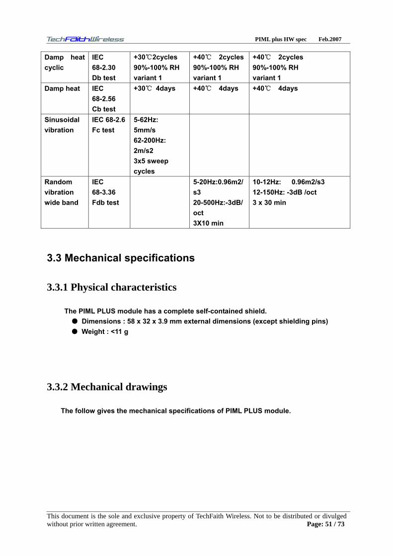
3.2 Environmental Specifications
Conditions Temperature range
Operating / Full GSM specification compliant - 10 to + 55
- 30 to + 85 Storage
TECHFAITH WIRELESS PIML PLUS
ENVIRONNEMENTAL CLASSES
TYPE TEST Standards Storage class 1.2
Transportation class 2.3
Operating (port use ) class 7.3
Cold IEC 68-2.1 Ab test
-25 72h -40 72h -20(GSM900) 16h -10(GSM1800/1900) 16h
Dry heat IEC 68-2.2 Bb test
+70 72h +70 72h +55 16h
Change of temperature
IEC 68-2.14 Na/Nb test
-40 /+30
5cycles t1=3h -20/30(GSM900) 3cycles -10/+30(GSM1800/1900): 3cycles t1=3h
This document is the sole and exclusive property of TechFaith Wireless. Not to be distributed or divulged without prior written agreement. Page: 50 / 73
PIML plus HW spec Feb.2007
This document is the sole and exclusive property of TechFaith Wireless. Not to be distributed or divulged without prior written agreement. Page: 51 / 73
Damp heat cyclic
IEC 68-2.30 Db test
+302cycles 90%-100% RH variant 1
+40 2cycles90%-100% RH variant 1
+40 2cycles 90%-100% RH variant 1
Damp heat IEC 68-2.56 Cb test
+30 4days +40 4days +40 4days
Sinusoidal vibration
IEC 68-2.6 Fc test
5-62Hz: 5mm/s 62-200Hz: 2m/s2 3x5 sweep cycles
Random vibration wide band
IEC 68-3.36 Fdb test
5-20Hz:0.96m2/s3 20-500Hz:-3dB/oct 3X10 min
10-12Hz: 0.96m2/s3 12-150Hz: -3dB /oct 3 x 30 min
3.3 Mechanical specifications
3.3.1 Physical characteristics
The PIML PLUS module has a complete self-contained shield. Dimensions : 58 x 32 x 3.9 mm external dimensions (except shielding pins)
Weight : <11 g
3.3.2 Mechanical drawings
The follow gives the mechanical specifications of PIML PLUS module.
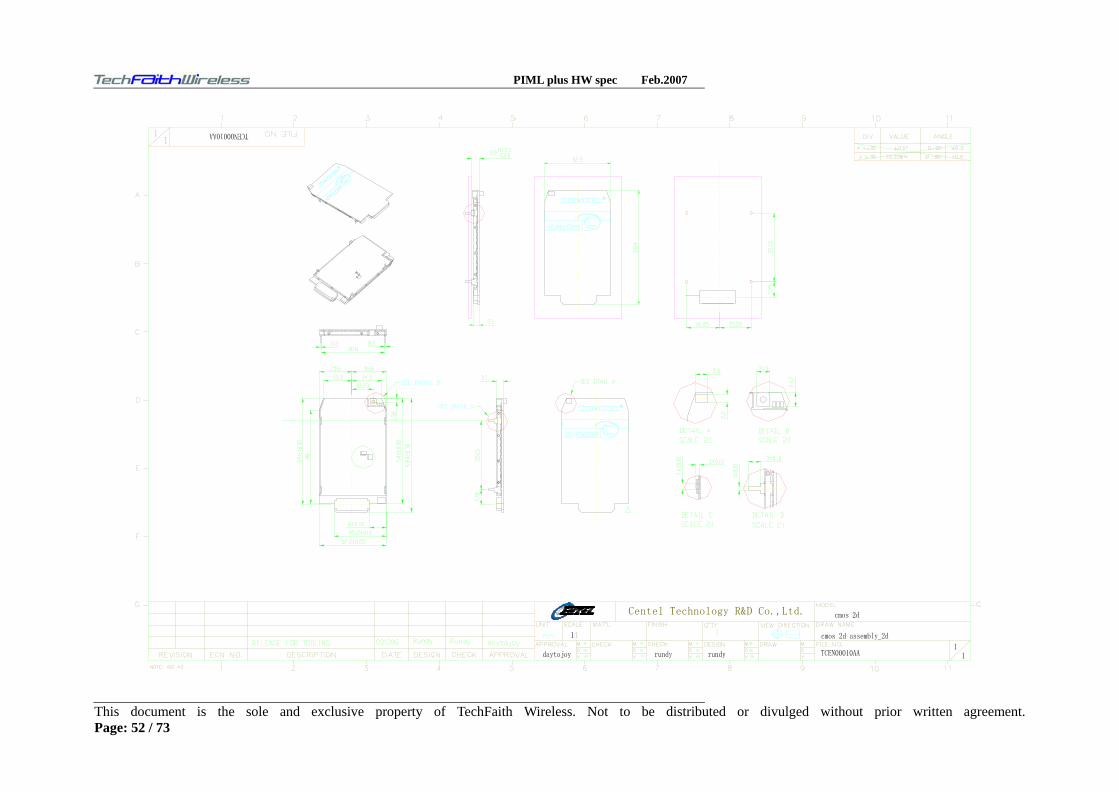
PIML plus HW spec Feb.2007
This document is the sole and exclusive property of TechFaith Wireless. Not to be distributed or divulged without prior written agreement. Page: 52 / 73
Centel Technology R&D Co.,Ltd.

PIML plus HW spec Feb.2007
4 Connectors and peripheral devices references
4.1 General Purpose Connector
The GPC is a 60 pins connector with 0.5mm pitch from KYOCERA / AVX group with the following reference:
14 5087 060 930 861.
The matting connector has the following reference: 24 5087 060 X00 861. 4
The stacking height is 3.0 mm. For further details see GPC data sheets in appendix. More information is also available from http://www.avxcorp.com
4 X=2 or 9
4.2 SIM Card Reader
Possible suppliers: ITT CANNON CCM03 series (see http://www.ittcannon.com) JAE (see http://www.jae.com )
AMPHENOL C707 series (see http://www.amphenol.com ) Drawer type :
MOLEX 99228-0002 (connector) / MOLEX 91236-0002 (holder) (see http://www.molex.com )
4.3 Microphone
Possible suppliers: PANASONIC HOSIDEN
This document is the sole and exclusive property of TechFaith Wireless. Not to be distributed or divulged without prior written agreement. Page: 53 / 73
PIML plus HW spec Feb.2007
4.4 Speaker
Possible suppliers: PHILIPS SANYO
HOSIDEN PRIMO
4.5 Antenna Cable
The following cable reference has been qualified for being mounted on PIML PLUS : MuRata MXTK92XXXX series RF cable.
4.6 GSM antenna
GSM antennas and support for antenna adaptation can be obtained from manufacturers such as: Galtronics Centurion
Amphenol
5 Design Guidelines
The purpose of the following paragraphs is to give design guidelines.
5.1 Hardware and RF
5.1.1 EMC recommendations
The EMC tests have to be performed as soon as possible on the application to detect any possible problem.
This document is the sole and exclusive property of TechFaith Wireless. Not to be distributed or divulged without prior written agreement. Page: 54 / 73
PIML plus HW spec Feb.2007
When designing, special attention should be paid to: Possible spurious emission radiated by the application to the RF receiver
in the receiver band ESD protection on SIM (if accessible from outside), serial link EMC protection on audio input/output (filters against 900MHz emissions) Bias of the Microphone inputs Length of the SIM interface lines (preferably <10cm) Ground plane : TECHFAITH WIRELESS recommends to have a common ground
plane for analog / digital / RF grounds. Metallic case or plastic casing with conductive paint are recommended
Note: The module does not include any protection against over voltage.
5.1.2 Power Supply
The power supply is one of the key issues in the design of a GSM terminal. A weak power supply design could affect in particular:
EMC performances the emissions spectrum
the phase error and frequency error Warning: Careful attention should be paid to: Quality of the power supply : Low ripple, PFM or PSM systems should be avoided (PWM
converter preferred). Capacity to deliver high current peaks in a short time (pulsed radio emission).
5.1.3 Layout requirement
This document is the sole and exclusive property of TechFaith Wireless. Not to be distributed or divulged without prior written agreement. Page: 55 / 73
PIML plus HW spec Feb.2007
This document is the sole and exclusive property of TechFaith Wireless. Not to be distributed or divulged without prior written agreement. Page: 56 / 73
PIML plus HW spec Feb.2007
5.1.4 Antenna
Warning: PIML PLUS strongly recommends to work with an antenna manufacturer either to develop an antenna adapted to the application or to adapt an existing solution to the application. The antenna adaptation (mechanical and electrical adaptation) is one of the key issues in the design of a GSM terminal.
5.2 Mechanical integration
Attention should be paid to: Antenna cable integration (bending, length, position, etc)
Legs of the module to be soldered on the Ground plane
5.3 Firmware upgrade
The PIML PLUS module firmware is stored in flash memory and it can easily be upgraded. In order to follow the regular evolutions of the GPRS standard and to offer state of the art software, TECHFAITH WIRELESS recommends that the application designed around a PIML PLUS (or PIML PLUS based product) allows easy firmware upgrades on the module via the standard Xmodem protocol. Therefore, the application shall either allow a direct access to the PIML PLUS serial link through an external connector or implement any mechanism allowing the PIML PLUS firmware to be downloaded via Xmodem. Two upgrade procedures are available: PC Loader Vision 3.85
5.3.1 Nominal upgrade procedure
The firmware file can be downloaded into the modem using the Xmodem protocol. To enter this mode, the AT+WDWL command (see description in the AT command manual) has to be sent. The necessary serial signals to proceed with the Xmodem downloading are: Rx, Tx, RTS, CTS and GND.
This document is the sole and exclusive property of TechFaith Wireless. Not to be distributed or divulged without prior written agreement. Page: 57 / 73

PIML plus HW spec Feb.2007
5.3.2 Backup procedure
In case the nominal upgrade mode is not possible (due to critical corruption on the flash memory), a backup procedure is also available. It requires TECHFAITH WIRELESS specific software to download the firmware file into the modem. This tool has to run on a PC connected to the serial bus of the modem. The necessary signals to proceed with the downloading are: Rx, Tx, RTS, CTS and GND. Prior to running the TECHFAITH WIRELESS downloader, the modem has to be set in download mode. Advise: To reduce the time of the download, it’s possible to change the speed of the serial link at 115200 bits/s. for that, you have to execute the AT command below : 1) AT+IPR=115200 2) AT+WDWL 3) File transfer 4) AT+CFUN=1 (reset of the module) Make attention that after the last command, the serial link will be by default at 9600 bits/s.
5.3.3 TechFaith PMIL Module Application Notes
Background: TechFaith’s PIML is based on Philip SysolME reference platform. Old part number of CPU in SysolME is OM6357EL3/3C5/7B. Application notes: The OM6357EL3/3C5/7B will have following characteristics: If there are voltage added onto GPIO and other pins of CPU before system launch up, this added voltage will goes through CPU and comes out onto some other pins of CPU. This can cause unexpected failure during powering up procedure, including unstable power up, unstable display and some unstable peripherals.
Be sure to control power up timing sequence in your system design. Never add voltage onto pins of new CPU before CPU powering up already.
This document is the sole and exclusive property of TechFaith Wireless. Not to be distributed or divulged without prior written agreement. Page: 58 / 73

PIML plus HW spec Feb.2007
6 Appendix
6.1 TECHFAITH WIRELESS acceptance test
These tests are TECHFAITH WIRELESS internal qualification tests. They are performed on a TECHFAITH WIRELESS evaluation platform (module on test board). Test
Applied standard Acceptance criteria
Performance test Mobile station (MS) conformance specification; Part 1: Conformance specification (release 5).
Full conformity to the recommendation regarding the main RF parameters.
3GPP TS 51.010 v5.0.0 (2002-09)Cooking test The test continues even after the
Cooking Test milestone has been reached
Stress test Thermal shocks IEC 68-2-14 Full conformity to the recommendation regarding the main parameters.
Vibration test Sinusoidal vibration IEC 68-2-6 No performance degradation or mechanical degradation is allow after test.
Shock test IEC 68-2-27 No performance degradation or mechanical degradation is allowed after test
Bump test IEC 68-2-29 No performance degradation or mechanical degradation is allowed at after test
Humidity test Corrosion test IEC 68-2-3 No visible degradation of the product, both visual and functional. The unit is tested at room temperature and must be fully operative for the main RF parameters.
Warehouse test Low temperance IEC 68-2-1 Under normal condition (room temperature) after the test, the unit must behave in full
This document is the sole and exclusive property of TechFaith Wireless. Not to be distributed or divulged without prior written agreement. Page: 59 / 73
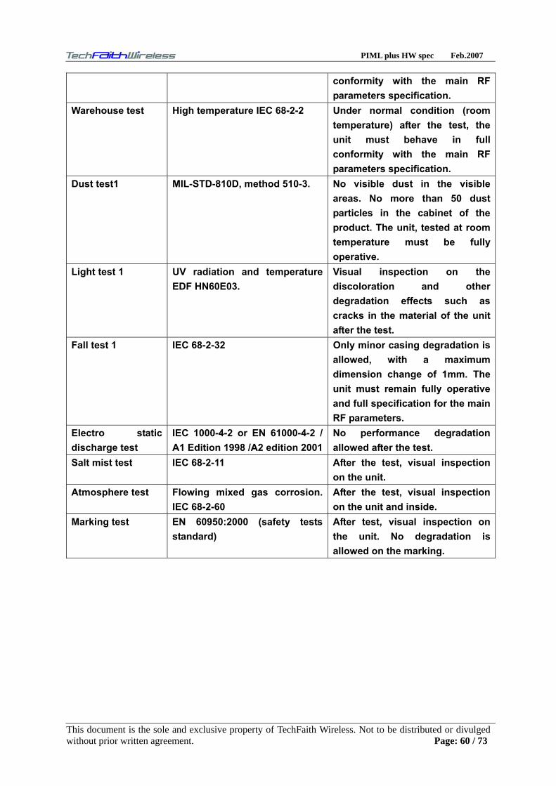
PIML plus HW spec Feb.2007
conformity with the main RF parameters specification.
Warehouse test High temperature IEC 68-2-2 Under normal condition (room temperature) after the test, the unit must behave in full conformity with the main RF parameters specification.
Dust test1 MIL-STD-810D, method 510-3. No visible dust in the visible areas. No more than 50 dust particles in the cabinet of the product. The unit, tested at room temperature must be fully operative.
Light test 1 UV radiation and temperature EDF HN60E03.
Visual inspection on the discoloration and other degradation effects such as cracks in the material of the unit after the test.
Fall test 1 IEC 68-2-32 Only minor casing degradation is allowed, with a maximum dimension change of 1mm. The unit must remain fully operative and full specification for the main RF parameters.
Electro static discharge test
IEC 1000-4-2 or EN 61000-4-2 / A1 Edition 1998 /A2 edition 2001
No performance degradation allowed after the test.
Salt mist test IEC 68-2-11 After the test, visual inspection on the unit.
Atmosphere test Flowing mixed gas corrosion. IEC 68-2-60
After the test, visual inspection on the unit and inside.
Marking test EN 60950:2000 (safety tests standard)
After test, visual inspection on the unit. No degradation is allowed on the marking.
This document is the sole and exclusive property of TechFaith Wireless. Not to be distributed or divulged without prior written agreement. Page: 60 / 73

PIML plus HW spec Feb.2007
6.2 Standards and Recommendations
GSM ETSI, 3GPP, GCF and NAPRD03 recommendations for Phase II.
Specification reference Title
3GPP TS 45.005 v5.5.0 (2002-08) Release 5
Technical specification group GSM/EDGE. Radio Access network; radio transmission and reception
GSM 02.07 v8.0.0 (1999-07)
Digital cellular telecommunications system (phase 2+); Mobile station features (GSM) 02.07 version 8.0.0 Release 1999
GSM 02.60 v8.1.0 (1999-07)
Digital cellular telecommunications system (Phase 2+); General Packet Radio Service (GPRS); Service description, stage 1 (GSM 02.60 version 8.1.0 Release 1999)
GSM 03.60 V7.9.0 (2002-09)
Technical specification group services and system aspects; Digital cellular telecommunications system (phase 2+); GPRS ; service description ; stage 2 (release 1998)
3GPP TS 43.064 V5.0.0(2002-04)
Technical specification group geran; digital cellular telecommunications system (phase 2+); general packet radio service ;overall description of the GPRS radio interface; Stage 2 (release 5)
3GPP TS 03.40 V7.5.0 (2001-12)
Technical specification group terminals; technical realization of the short message service (SMS) (Release 1998)
3GPP TS 03.41 V7.4.0 (2000-09)
Technical Specification Group terminals; Technical realization of Cell broadcast service (CBS) (Release 1998)
ETSI EN 300 903 V8.1.1(2000-11)
Digital cellular telecommunications system (phase 2+); transmission planning aspects of the speech service in the GSMPublic Land Mobile Network (PLMN) system (GSM) 03.50 version 8.1.1 (Release 1999)
3GPP TS 04.06 V8.2.1(2002-05)
Technical specification Group GSM/EDGE Radio Access Network; Mobile station – base station system (MS - BSS) interface; Data Link (DL) layer specification (release 1999)
3GPP TS 04.08 V7.18.0(2002-09)
Technical specification group core network; digital cellular telecommunications system (phase 2+); Mobile radio interface layer 3 specification (release 1998)
3GPP TS 04.10 V7.1.0 (2001 - 12)
Technical specification group core network; mobile radio interface layer 3 supplementary services specification; general aspects (release 1998)
3GPP TS 45.005 V5.5.0 (2002-08)
technical Specification Group GSM/EDGE. Radio (2002-08) Access Network; Radio transmission and reception (Release 5)
This document is the sole and exclusive property of TechFaith Wireless. Not to be distributed or divulged without prior written agreement. Page: 61 / 73

PIML plus HW spec Feb.2007
3GPP TS 45.008 V5.8.0 (2002-08)
Technical Specification Group GSM/EDGE Radio Access Network; Radio subsystem link control (Release 5)
3GPP TS 45.010 V5.1.0 (2002-08)
Technical Specification Group GSM/EDGE Radio Access Network; Radio subsystem synchronization (Release 5)
3GPP TS 46.010 V5.0.0 (2002-06)
Technical Specification Group Services and System Aspects; Full rate speech; Transcoding (Release 5)
3GPP TS 46.011 V5.0.0 (2002-06)
Technical Specification Group Services and System Aspects; Full rate speech; Substitution and muting of lost frames for full rate speech channels (Release 5)
3GPP TS 46.012 V5.0.0 (2002-06)
Technical Specification Group Services and System Aspects; Full rate speech; Comfort noise aspect for full rate speech traffic channels (Release 5)
3GPP TS 46.031 V5.0.0 (2002-06)
Technical Specification Group Services and System Aspects; Full rate speech; Discontinuous Transmission (DTX) for full rate speech traffic channels (Release 5)
3GPP TS 46.032 V5.0.0 (2002-06)
Technical Specification Group Services and System Aspects; Full rate speech; Voice Activity Detector (VAD) for full rate speech traffic channels (Release 5)
TS 100 913V8.0.0 (1999-08)
Digital cellular telecommunications system (Phase 2+); General on Terminal Adaptation Functions (TAF) for Mobile Stations (MS) (GSM 07.01 version 8.0.0 Release 1999)
GSM 09.07 V8.0.0 (1999-08)
Digital cellular telecommunications system (Phase 2+); General requirements on interworking between the Public Land Mobile Network (PLMN) and the Integrated Services Digital Network (ISDN) or Public Switched Telephone Network (PSTN) (GSM 09.07 version 8.0.0 Release 1999)
3GPP TS 51.010-1 v5.0.0(2002-09)
Technical specification group GSM/EDGE; Radio Access Network; Digital cellular telecommunications system (phase 2+);Mobile station (MS) conformance specification; Part 1: Conformance specification(release 5)
3GPP TS 51.011 V5.0.0 (2001-12)
technical Specification Group Terminals; Specification of the Subscriber Identity Module - Mobile Equipment (SIM - ME) interface (Release 5)
ETS 300 641 (1998-03) Digital cellular telecommunications system (Phase 2); Specification of the 3 Volt Subscriber Identity Module -Mobile Equipment (SIM-ME) interface (GSM 11.12 version 4.3.1)
This document is the sole and exclusive property of TechFaith Wireless. Not to be distributed or divulged without prior written agreement. Page: 62 / 73

PIML plus HW spec Feb.2007
GCF-CC V3.7.1 (2002-08)
Global Certification Forum -Certification Criteria
NAPRD03 V2.6.0 (2002-06)
North America Permanent Reference Document for PTCRB tests
6.3 Safety recommendations (for information only)
IMPORTANT FOR THE EFFICIENT AND SAFE OPERATION OF YOUR GSM APPLICATION BASED ON TECHFAITH WIRELESS PIML PLUS Series PLEASE READ THIS INFORMATION CAREFULLY
6.3.1 RF safety
6.3.1.1 General
Your GSM terminal6 is based on the GSM standard for cellular technology. The GSM
standard is spread all over the world. It covers Europe, Asia and some parts of America and Africa. This is the most used telecommunication standard. Your GSM terminal is actually a low power radio transmitter and receiver. It sends out and receives radio frequency energy. When you use your GSM application, the cellular system that handles your calls controls both the radio frequency and the power level of your cellular modem.
6.3.1.2 Exposure to RF energy
There has been some public concern about possible health effects of using GSM terminals. Although research on health effects from RF energy has focused on the current RF technology for many years, scientists have begun research regarding newer radio technologies, such as GSM. After existing research had been reviewed, and after compliance to all applicable safety standards had been tested, it has been concluded that the product was fitted for use. If you are concerned about exposure to RF energy there are things you can do to minimize
This document is the sole and exclusive property of TechFaith Wireless. Not to be distributed or divulged without prior written agreement. Page: 63 / 73

PIML plus HW spec Feb.2007
exposure. Obviously, limiting the duration of your calls will reduce your exposure to RF energy. In addition, you can reduce RF exposure by operating your cellular terminal efficiently by following the below guidelines. 5 based on PIML PLUS
6.3.1.3 Efficient terminal operation
For your GSM terminal to operate at the lowest power level, consistent with satisfactory call quality: If your terminal has an extendible antenna, extend it fully. Some models allow you to place a call with the antenna retracted. However your GSM terminal operates more efficiently with the antenna fully extended. Do not hold the antenna when the terminal is <IN USE > Holding the antenna affects call quality and may cause the modem to operate at a higher power level than needed.
6.3.1.4 Antenna care and replacement
Do not use the GSM terminal with a damaged antenna. If a damaged antenna comes into contact with the skin, a minor burn may result. Replace a damaged antenna immediately. Consult your manual to see if you may change the antenna yourself. If so, use only a manufacturer-approved antenna. Otherwise, have your antenna repaired by a qualified technician. Use only the supplied or approved antenna. Unauthorized antennas, modifications or attachments could damage the terminal and may contravene local RF emission regulations or invalidate type approval.
This document is the sole and exclusive property of TechFaith Wireless. Not to be distributed or divulged without prior written agreement. Page: 64 / 73

PIML plus HW spec Feb.2007
6.3.2 General safety
6.3.2.1 Driving
Check the laws and the regulations regarding the use of cellular devices in the area where you have to drive as you always have to comply with them. When using your GSM terminal while driving, please: give full attention to driving, pull off the road and park before making or answering a call if driving
conditions so require.
6.3.2.2 Electronic devices
Most electronic equipment, for example in hospitals and motor vehicles is shielded from RF energy. However RF energy may affect some improperly shielded electronic equipment.
6.3.2.3 Vehicle electronic equipment
Check your vehicle manufacturer representative to determine if any on-board electronic equipment is adequately shielded from RF energy.
6.3.2.4 Medical electronic equipment
Consult the manufacturer of any personal medical devices (such as pacemakers, hearing aids, etc...) to determine if they are adequately shielded from external RF energy. Turn your terminal OFF in health care facilities when any regulations posted in the area instruct you to do so. Hospitals or health care facilities may be using RF monitoring equipment.
6.3.2.5 Aircraft
Turn your terminal OFF before boarding any aircraft. Use it on the ground only with crew permission.
This document is the sole and exclusive property of TechFaith Wireless. Not to be distributed or divulged without prior written agreement. Page: 65 / 73

PIML plus HW spec Feb.2007
Do not use it in the air. To prevent possible interference with aircraft systems, Federal Aviation Administration (FAA) regulations require you to have permission from a crew member to use your terminal while the aircraft is on the ground. To prevent interference with cellular systems, local RF regulations prohibit using your modem while airborne.
6.3.2.6 Children
Do not allow children to play with your GSM terminal. It is not a toy. Children could hurt themselves or others (by poking themselves or others in the eye with the antenna, for example). Children could damage the modem, or make calls that increase your modem bills.
6.3.2.7 Blasting areas
To avoid interfering with blasting operations, turn your unit OFF when in a <blasting area > or in areas posted : <turn off two-way radio> Construction crew often use remote control RF devices to set off explosives.
6.3.2.8 Potentially explosive atmospheres
Turn your terminal OFF when in any area with a potentially explosive atmosphere. It is rare, but your modem or its accessories could generate sparks. Sparks in such areas could cause an explosion or fire resulting in bodily injuries or even death. Areas with a potentially explosive atmosphere are often, but not always, clearly marked. They include fuelling areas such as petrol stations; below decks on ships; fuel or chemical transfer or storage facilities; and areas where the air contains chemicals or particles, such as grain, dust, or metal powders. Do not transport or store flammable gas, liquid, or explosives, in the compartment of your vehicle which contains your terminal or accessories. Before using your terminal in a vehicle powered by liquefied petroleum gas (such as propane or butane) ensure that the vehicle complies with the relevant fire and safety
This document is the sole and exclusive property of TechFaith Wireless. Not to be distributed or divulged without prior written agreement. Page: 66 / 73

PIML plus HW spec Feb.2007
regulations of the country in which the vehicle is to be used.
6.4 Application notes for the SIM interface
The next pages are application notes to interface the module with SIM cards: application note: Interface with 3V SIMs
SIMs interface layout: · C1,C2,C3,C4 be closed with SIM socket as possible. · add ESD protect component between all signals and GND.
6.5 General Purpose Connector data sheet
The next 6 pages are the KYOCERA/ELCO data sheets for the GPC (also available from http://www.avxcorp.com.
This document is the sole and exclusive property of TechFaith Wireless. Not to be distributed or divulged without prior written agreement. Page: 67 / 73

PIML plus HW spec Feb.2007
This document is the sole and exclusive property of TechFaith Wireless. Not to be distributed or divulged without prior written agreement. Page: 68 / 73

PIML plus HW spec Feb.2007
This document is the sole and exclusive property of TechFaith Wireless. Not to be distributed or divulged without prior written agreement. Page: 69 / 73

PIML plus HW spec Feb.2007
This document is the sole and exclusive property of TechFaith Wireless. Not to be distributed or divulged without prior written agreement. Page: 70 / 73

PIML plus HW spec Feb.2007
This document is the sole and exclusive property of TechFaith Wireless. Not to be distributed or divulged without prior written agreement. Page: 71 / 73
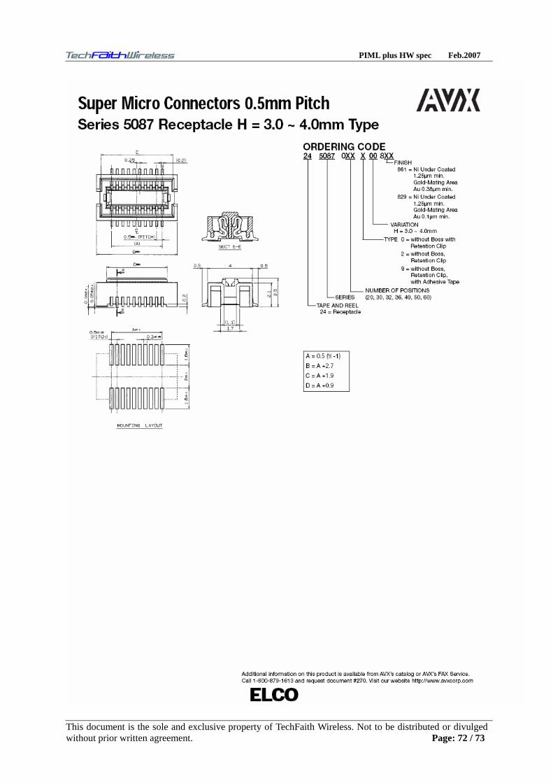
PIML plus HW spec Feb.2007
This document is the sole and exclusive property of TechFaith Wireless. Not to be distributed or divulged without prior written agreement. Page: 72 / 73

PIML plus HW spec Feb.2007
This document is the sole and exclusive property of TechFaith Wireless. Not to be distributed or divulged without prior written agreement. Page: 73 / 73