piezoresponse force microscopy behaviour of bi ti … 11 01.pdf · piezoresponse force microscopy...
TRANSCRIPT

1
Processing and Application of Ceramics 5 [1] (2011) 1–11
Piezoresponse force microscopy behaviour of Bi4Ti3O12 ceramics with various excess bismuthEderson C. Aguiar1, Alexandre Z. Simões2,*, Francisco Moura3, Mario Cilense1, Elson Longo1, Jose A. Varela1
1São Paulo State University, UNESP, Chemistry Institute, Department of Chemistry-Physics, P.O Box 355, 14800-900, Araraquara, São Paulo, Brazil2São Paulo State University, UNESP, Engineering Faculty, P.O Box 355, 12516-410, Guaratinguetá, São Paulo, Brazil3Federal University of Itajubá- Unifei - Campus Itabira, Rua São Paulo 377, Bairro Amazonas, P.O. Box 355, 35900-37, Itabira, Minas Gerais, BrazilReceived 19 November 2010; received in revised form 21 January 2011; accepted 14 February 2011
AbstractBismuth titanate (Bi4Ti3O12 - BIT) ceramics derived from different amounts of excess Bi2O3 were prepared using the polymeric precursor method. In spite of excess bismuth, single phase ceramics were obtained with a con-trolled microstructure. Raman analysis evidenced typical vibrational bands of the BIT phase. UV-vis spectra indicated that excess Bi2O3 causes a reduction in defects in the BIT lattice due to the suppression of oxygen vacancies located at the octahedral BO6
– ion. The microstructure and electrical properties are strongly depen-dent on the excess Bi2O3. Appropriate initial Bi2O3 excess reduces the leakage current and loss tangent and thereby improves the polarization of BIT ceramics. Rietveld analyses confirmed that the powders crystallize in an orthorhombic structure with a space group of Fmmm at room temperature. The polarization reversal was investigated by applying ac voltage through a conductive tip during the area scanning and was investigated by piezoresponse force microscopy (PFM).
Keywords: bismuth titanate, chemical synthesis, annealing, dielectric properties
I. IntroductionRecently, compounds with an Aurivillius struc-
ture have been investigated, such as: BBT (barium bismuth tantalate), SBN (strontium bismuth niobate), SBT (strontium bismuth titanate), BBN (barium bis-muth niobate) and BIT (bismuth titanate). BIT is a promising ferroelectric material which is used in non-volatile random access memories [1,2]. Bi4Ti3O12 has interesting properties: high Curie temperature, high remanent polarization and low coercive field. These properties are due to the Bi2O2 layers separated by per-ovskite planes of type Bi2Ti3O10 in the orthorhombic structure. The crystal structures of BLSFs (bismuth-layer-structured ferroelectrics) are generally formu-lated as (Bi2O2)
2+(Am-1BmO3m+1)2- where A represents
mono-, di-, or trivalent ions, B represents tetra-, pen-ta-, or hexavalent ions with appropriate size and va-lence, and m is the number of BO6 octahedra in the pseudoperovskite blocks (m = 1, 2, 3, 4, and 5). The perovskite blocks, (Am-1BmO3m+1)
2-, are sandwiched be-tween bismuth oxide layers, (Bi2O2)
2+ along the c-axis [3]. The electric and dielectric properties of the blocks have been improved by the addition of excess bismuth. These studies revealed that when the value of the ex-cess Bi content in precursor sols is 10 mol% the best polarization-electric field, capacitance-voltage and di-electric characteristics were attained. Also, the addi-tion of a 3 mol% excess of Bi2O3 resulted in a dras-tic decrease in the leakage current [4,5]. The excess Bi2O3 in SBT indicated that the phase-transition and ferroelectric properties such as spontaneous polariza-tion (Ps) showed a dependence on the Bi content. The ferroelectric Curie temperature Tc decreased with an
* Corresponding author: tel: +55 12 3123 2765fax: +55 12 3123 2800, e-mail: [email protected]

2
E.C. Aguiar et al. / Processing and Application of Ceramics 5 [1] (2011) 1-11
increasing in the Bi content and the Ps was maximized when 2–3 mol% excess of Bi2O3 was added [6]. In oth-er work, addition of 10 mol% Bi excess in BaBi2Ta2O9 increased the dielectric permittivity with decreasing tan δ while improve ferroelectric properties [7]. In an-other experiment, bismuth titanate with an excess of 5 wt.% Bi was added to the stoichiometic mixture aim-ing to minimize the bismuth loss during the thermal treatment. Without the addition of bismuth, pure phase could not be obtained [8].
Due to this high transition temperature, BIT ceram-ics are good candidates for high temperature piezoelec-tric applications. The main problem concerning their practical application as piezoelectrics is the relatively low electrical resistivity. The electrical conductivity in BIT is highly anisotropic, with the maximum value in the same plane of the vector polarization. As a conse-quence, BIT ceramics are very difficult to pole. Thus the reduction of electrical conductivity is one of the main goals the worldwide investigations of BIT [9].
The BIT-based ceramics microstructure reflects the structural anisotropy showing larger platelets-like grains growing preferentially in the a–b plane. The electrical response of these materials is strongly dependent on the microstructure [10,11]. The conventional ceramic route synthesis leads to undesireable phases due to volatil-ization of Bi2O3 at elevated temperatures [12]. The for-mation of secondary phases can be avoided by decreas-ing the calcination temperature or using wet-chemistry based methods. By using chemical methods, (e.g. co-precipitation, sol-gel, hydrothermal and the Pechini method [13]), it is possible to control the morphology and chemical composition of the powders. Due to the easy volatilization of Bi2O3 in the fabrication process, initial excess bismuth can strongly affect the structure and physical properties of the Bi4Ti3O12-based materi-als. Kim and Kim [14] studied the effect of excess bis-muth on the crystallization of BLT thin film prepared by MOD. Lin et al. [15] studied the role of excess bismuth on the orientation and ferroelectricity of BLT film by CSD. However, limited research has been conducted re-lated to the microscopic effect that excess bismuth can cause in Bi4Ti3O12-based ceramics. The aim of this paper is to examine the effects of initial Bi2O3 excess content on microstructural and electrical properties of Bi4Ti3O12 (BIT) ceramics. To vary the Bi2O3 content, the ceram-ics derived from varying amount of initially excess of Bi2O3 (3–10 mol%) on the precursor solution were pre-pared by the polymeric precursor method. Measure-ments by piezoresponse force microscopy (PFM) reveal that addition of excess bismuth can reduce the strain en-ergy and pin-charged defects and that the perpendicu-lar component of polarization can be switched between two stable states: bright and dark contrast inside and outside of the square region.
II. ExperimentalTitanium isopropoxide (97% - Alfa Aesar); bismuth
nitrate pentahydrate (100.1% - Mallinckrodt); citric acid (99.5% - Merck); ethlyleneglycol (99.7% - Synth), nitric acid (99.9% - Synth); ethylenediamine (98% - Nuclear) and ammonium hydroxide (99.9% - Qhemis) were used as raw materials. Bismuth and titanium pre-cursor solutions were prepared by adding the raw ma-terials to ethylene glycol and concentrated aqueous cit-ric acid under heating and stirring. The molar ratio of metal : citric acid : ethylene glycol was 1 : 4 : 16. Ap-propriate quantities of Ti and Bi solutions were mixed and homogeneized by stirring at 90°C for 2 hours. Then the temperature was increased to 130–140°C, yield-ing a highly viscous polyester resin. Most of the or-ganic material was decomposed by thermal treatment at 300°C for 2 hours. The formed porous product was crushed and heated in an aluminium crucible at 700°C for 4 hours to eliminate residues of organic material. The powders were milled for 4 hours with zirconia balls and isopropyl alcohol with and without excess Bi. The bismuth titanate compositions were designed as BIT, BIT3, BIT5 and BIT10 which corresponds to 0, 3, 5 and 10 mol% of excess Bi2O3. The powders were uniax-ialy (150 MPa) and isostatically pressed (210 MPa) into pellets. The sintering was performed on pellets packed into covered alumina crucibles, carried out in air at a temperature of 800°C for 1 hour (heating and cooling rate of 10 °C/min).
Raman scattering of powders was performed at room temperature (Fourier transform - RFS 100/S Bruker, excited by a Nd-YAG laser in 1064 nm). The band gap values were obtained using ultraviolet spec-troscopy in the visible region curve (UV-vis-NIR Spectrophotometer - Varian Cary 500 X). For Rietveld analyses, X-ray diffraction data were collected with a Rigaku 20-2000 diffractometer under the following experimental conditions: 40 kV, 30 mA, 2θ from 20° to 120°, step size of 0.02°, λCu Kα monocromatized by a graphite crystal, divergence slit of 2 mm, recep-tion slit of 0.6 mm and step time of 10 s. The Riet-veld analysis was performed with the Rietveld refine-ment program DBWS-941 1 [16]. The profile function used was the modified Thompson-Cox-Hasting pseu-do-Voigt, in which η (the Lorentzian fraction of the function) varies with the Gauss and Lorentz compo-nents of the full width at half maximum.
Bulk densities and weight loss of the sintered pellets were measured by the Archimedes method. The phase formation and crystallinity were studied by X-ray dif-fractometry (XRD) with Cu Kα radiation using a nor-mal θ-2θ scanning method (Rigaku RINT2000 diffrac-tometer). A scanning electron microscope (SEM) was used to analyze the morphology and shape of the grains (Topcom SM-300).
3
E.C. Aguiar et al. / Processing and Application of Ceramics 5 [1] (2011) 1-11
Dielectric permittivity measurements were performed in HP 4192A LF Mountain View impedancemeter at-tached to a Flyever oven (FE50RP temperature control-ler). Silver electrodes for electrical measurements were deposited on the polished surface of sintered pellets by evaporation through a sputtering system. Resistivity was determined by current-voltage in a voltage source (Keit-ley 237 - USA).
Piezoelectric measurements were carried out using a setup based on an atomic force microscope in a Mul-timode Scanning Probe Microscope with Nanoscope IV controller (Veeco FPP-100). In our experiments, piezo-response images were acquired in ambient air by apply-ing a small ac voltage with amplitude of 2.5 V (peak to peak) and a frequency of 10 kHz. To apply the external voltage a standard-gold coated Si3N4 cantilever with a spring constant of 0.09 N/m was used. The probing tip, with an apex radius of about 20 nm, was in mechani-cal contact with the uncoated film surface during the measurements. Cantilever vibration was detected using a conventional lock-in technique.
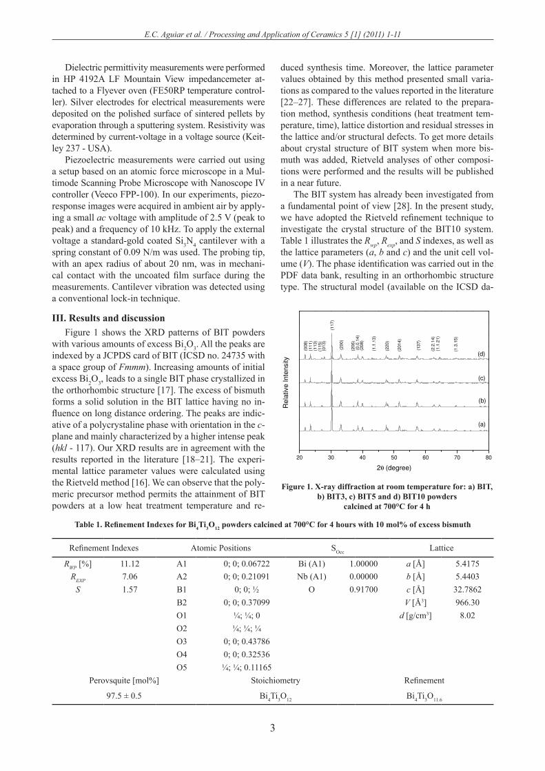
III. Results and discussionFigure 1 shows the XRD patterns of BIT powders
with various amounts of excess Bi2O3. All the peaks are indexed by a JCPDS card of BIT (ICSD no. 24735 with a space group of Fmmm). Increasing amounts of initial excess Bi2O3, leads to a single BIT phase crystallized in the orthorhombic structure [17]. The excess of bismuth forms a solid solution in the BIT lattice having no in-fluence on long distance ordering. The peaks are indic-ative of a polycrystaline phase with orientation in the c-plane and mainly characterized by a higher intense peak (hkl - 117). Our XRD results are in agreement with the results reported in the literature [18–21]. The experi-mental lattice parameter values were calculated using the Rietveld method [16]. We can observe that the poly-meric precursor method permits the attainment of BIT powders at a low heat treatment temperature and re-
duced synthesis time. Moreover, the lattice parameter values obtained by this method presented small varia-tions as compared to the values reported in the literature [22–27]. These differences are related to the prepara-tion method, synthesis conditions (heat treatment tem-perature, time), lattice distortion and residual stresses in the lattice and/or structural defects. To get more details about crystal structure of BIT system when more bis-muth was added, Rietveld analyses of other composi-tions were performed and the results will be published in a near future.
The BIT system has already been investigated from a fundamental point of view [28]. In the present study, we have adopted the Rietveld refinement technique to investigate the crystal structure of the BIT10 system. Table 1 illustrates the Rwp, Rexp, and S indexes, as well as the lattice parameters (a, b and c) and the unit cell vol-ume (V). The phase identification was carried out in the PDF data bank, resulting in an orthorhombic structure type. The structural model (available on the ICSD da-
Figure 1. X-ray diffraction at room temperature for: a) BIT, b) BIT3, c) BIT5 and d) BIT10 powders
calcined at 700°C for 4 h
Table 1. Refinement Indexes for Bi4Ti3O12 powders calcined at 700°C for 4 hours with 10 mol% of excess bismuth
Refinement Indexes Atomic Positions SOcc Lattice
RWP [%] 11.12 A1 0; 0; 0.06722 Bi (A1) 1.00000 a [Å] 5.4175REXP 7.06 A2 0; 0; 0.21091 Nb (A1) 0.00000 b [Å] 5.4403
S 1.57 B1 0; 0; ½ O 0.91700 c [Å] 32.7862B2 0; 0; 0.37099 V [Å3] 966.30O1 ¼; ¼; 0 d [g/cm3] 8.02O2 ¼; ¼; ¼O3 0; 0; 0.43786O4 0; 0; 0.32536O5 ¼; ¼; 0.11165
Perovsquite [mol%] Stoichiometry Refinement
97.5 ± 0.5 Bi4Ti3O12 Bi4Ti3O11.6
1
20 30 40 50 60 70 80
Re
lative
Inte
nsity
2θ (degree)
(a)
(b)
(c)
(008
)(1
11
)(1
13
)(1
15
)(0
13
)
(117
)
(20
0)
(206
)(0
.0.1
4)
(20
8)
(220
)
(201
4)
(13
7)
(2.2
.14)
(1.1
.21)
(1.3
.15
)
(d)
(1.1
.13
)
Figure 1 - X-ray diffraction for BIT powders calcined at 700°C -4h: (a) BIT, (b) BIT3, (c) BIT5,
(d) BIT10.

4
E.C. Aguiar et al. / Processing and Application of Ceramics 5 [1] (2011) 1-11
tabank) that allows the best fit was the orthorhombic model (ICSD no. 24735 with a space group of Fmmm). Quantitative phase analyses for the orthorhombic phase were calculated according to the reference of Young and Wiles [16]. The covalent interaction originating from the strong hybridization between Ti 3d and O 2p or-bitals, plays an important role in the structural distor-tion of the BIT compound. It can be assumed that addi-tion of excess of bismuth improves oxygen ion stability in the lattice because some of the Bi ions in the pseudo-perovskite layers containing Ti–O octahedral were not volatilized. The low S values (S = Rwp/Rexp) indicates the good quality of the refinement; the calculated parame-ters are closer to literature data [29]. Therefore, we can assume that the addition of excess bismuth stabilizes the oxygen vacancies and consequently the structure.
The weight loss and relative density as a function of excess Bi2O3 are shown in Fig. 2. It can be seen that the weight loss increases with increasing excess Bi2O3 be-cause the low temperature sintering inhibits bismuth ox-ide volatilization. The relative density measured by the Archimedes method increases with excess Bi2O3 reach-ing around 90% of the theoretical density of BIT, corre-sponding to 8.038 g/cm3. This result is not satisfactory from an electrical point of view, since the polarization and dielectric permittivity are dependent on the level of porosity and grains morphology, but it is still a very in-teresting effect.
UV-vis spectroscopy measurements were evaluated in the BIT powders (see Fig. 3). The maximum absorp-tion was located at around 400 nm with respective band gap values determined from the Kubelka Model [30]. The optical energy band gap is related to the absorbance and to the photon energy by the following equation:
hνα ∝ (hº - Egopt)2 (1)
where α is the absorbance, h is the Planck constant, ν is the frequency and Eg
opt is the optical band gap [31]. The obtained values are 3.13, 3.02, 3.03, 3.03 eV, which are similar to the values reported by Wei et al. [32] (around
3
2,0 2,5 3,0 3,5 4,0
Inte
nsity (
a.u
.)
Gap energy (eV)
2,0 2,5 3,0 3,5 4,0
Inte
nsity (
a.u
.)
Gap Energy (eV)
(a) (b)
2,0 2,5 3,0 3,5 4,0
Inte
nsity (
a.u
.)
Gap Energy (eV)
2,0 2,5 3,0 3,5 4,0
Inte
nsity (
a.u
.)
Gap Energy (eV)
(c) (d)
Figure 3 - UV-vis absorption spectra at room temperature for BIT, BIT3, BIT5 and BIT10 powders
calcined at 700°C -4h.
3
2,0 2,5 3,0 3,5 4,0
Inte
nsity (
a.u
.)
Gap energy (eV)
2,0 2,5 3,0 3,5 4,0
Inte
nsity (
a.u
.)
Gap Energy (eV)
(a) (b)
2,0 2,5 3,0 3,5 4,0
Inte
nsity (
a.u
.)
Gap Energy (eV)
2,0 2,5 3,0 3,5 4,0
Inte
nsity (
a.u
.)Gap Energy (eV)
(c) (d)
Figure 3 - UV-vis absorption spectra at room temperature for BIT, BIT3, BIT5 and BIT10 powders
calcined at 700°C -4h.
3
2,0 2,5 3,0 3,5 4,0
Inte
nsity (
a.u
.)
Gap energy (eV)
2,0 2,5 3,0 3,5 4,0
Inte
nsity (
a.u
.)
Gap Energy (eV)
(a) (b)
2,0 2,5 3,0 3,5 4,0
Inte
nsity (
a.u
.)
Gap Energy (eV)
2,0 2,5 3,0 3,5 4,0
Inte
nsity (
a.u
.)
Gap Energy (eV)
(c) (d)
Figure 3 - UV-vis absorption spectra at room temperature for BIT, BIT3, BIT5 and BIT10 powders
calcined at 700°C -4h.
Figure 3. UV-vis absorption spectra at room temperature for: a) BIT, b) BIT3, c) BIT5 and d) BIT10 powders
calcined at 700°C for 4 h
a)
c)
b)
d)
Figure 2. Relative density and weight loss of the sinteredpellets versus excess bismuth
2
0 2 4 6 8 10
0,65
0,70
0,75
0,80
0,85
Bi excess (mol%)
We
igh
t lo
ss (
%)
65
70
75
80
85
90
95
100
Re
lativ
e d
en
sity
(%)
Figure 2 - Relative density and weight loss of the sintered pellets versus excess bismuth.

5
E.C. Aguiar et al. / Processing and Application of Ceramics 5 [1] (2011) 1-11
3.08 eV). Our BIT powders presented characteristic absorption spectra of ordered or crystalline materials. These results indicate that the exponential optical ab-sorption edge and the optical band gap are controlled by the degree of structural disorder in the BIT lattice. This decrease in the band gap can be ascribed to a reduction of defects in the lattice which decreases the interme-diary energy levels due to the reduction of oxygen va-cancies located at BO6 octahedra. The main differences in optical band gaps can be related to the different fac-tors, mainly including: synthesis method, shape (pow-der, crystal or thin film) and synthesis conditions.
Raman scattering has proven to be a valuable tech-nique to obtain information about local structures with-in materials. Figure 4 shows the Raman spectra of BIT powders derived from different excess Bi2O3 at room temperature. To better denote the peak position, Raman modes are presented in Table 2. The order-disorder de-gree in the crystal lattice of BIT powders at short and medium distances was investigated. Raman modes lo-cated at 96, 119, 189, 223, 266, 315, 450, 536, 615 and 848 cm-1 are characteristics of the BIT phase [33]. The modes located under 200 cm-1 can be related to vibra-tions between Bi and O atoms [34]. For BIT10, it is evidently a characteristic mode around 100 cm-1 and is probably due to a distortion in the A site caused by the bismuth ion. This distortion into the A site of the perovskite enhances the Jahn-Teller distortion of TiO6 octahedra. On the other hand, Raman modes located above 200 cm-1 are responsible for distortions and vi-brations of TiO6 octahedra. As the content of excess bis-muth increases, there is a reduction in the Raman band intensities, (mainly the mode located at 266 cm-1). This is due to the vibrations of Ti-O atoms inside the per-ovskite layer and to vibrations of Bi-O atoms within the Bi2O2 layer [35]. The main bands at 266, 536 and 848 cm-1, originated from TiO6 octahedra, share a similar excess bismuth behaviour (they reduce its intensity and become broaden with increasing Bi excess). The modes at 230, 268, 328, 530, 563 and 850 cm-1 are assigned to stretching and bending vibrations of TiO6 octahedra be-cause the addition of excess Bi2O3 implies a distortion of Bi2O2 layers. Raman results are in agreement with XRD data. The appearance of a Raman mode at low-frequency (96 cm-1) is due to the atomic mass of Bi ions which causes Bi displacements in the Bi2O2 layer [36]. Raman modes located at 450 and 96 cm-1 were evident in BIT10 composition, indicating that 10 mol% of ex-
cess bismuth may cause lattice distortions and stoicho-metric changes. Raman results are in agreement with XRD data, indicating an ordered structure at short and long distances.
The microstructures of the sintered pellets were ex-amined by SEM analyses and are illustrated in Fig. 5. The influence of excess bismuth on the shape and size of the grains was evaluated. The grain size is hetero-geneously distributed and presents rod-like form mor-phology which is different from literature data [37]. BIT presents a porous microstructure with compact re-gion with a very small grain size when compared to ceramics with excess bismuth. The BIT3, BIT5 and BIT10 compositions are dense but pure BIT is prone to form a porous structure with a quite a number of voids which can affect the ferroelectric and dielectric proper-ties of ceramics. All ceramics are stoichiometric, evi-dencing no losses of Bi2O3 during the calcination and sintering process indicating that the initial Bi2O3 excess is sufficient to compensate for the bismuth oxide vola-tilization and fill the Bi vacancy in the lattice. Literature data revealed that some excess of bismuth in the BIT ceramic cannot enter into the lattice. The Bi2O3 excess may exist as an impurity phase such as bismuth oxide, which would affect the microstructural and ferroelec-tric properties of ferroelectric material [38]. The den-sities of BIT ceramics increase with content of excess bismuth due to the formation of oxygen vacancies orig-inate during the calcinated process of the ceramics and substitution of excess of bismuth. That leads to nega-
Figure 4. Raman spectra at room temperature for: a) BIT, b) BIT3, c) BIT5 and d) BIT10 powders calcined
at 700°C for 4 h
4
0 200 400 600 800 1000
96
Inte
nsity (
a.u
.)
Raman shift (cm-1)
119
189
223
266
315
45
0
53
6
615
848
(a)
(b)
(c)
(d)
Figure 4 - Raman spectra at room temperature for BIT, BIT3, BIT5 and BIT10 powders calcined at
700°C -4h.
Table 2. Raman modes of Bi4Ti3O12 powders calcinated at 700°C for 4 hours with several excess bismuth
Compositions Raman modes [cm-1]BIT 119, 189, 223, 266, 315, 536, 615, 848
BIT3 119, 189, 223, 266, 315, 536, 615, 848BIT5 119, 189, 223, 266, 315, 536, 615, 848BIT10 96, 119, 189, 223, 266, 315, 450, 536, 615, 848

6
E.C. Aguiar et al. / Processing and Application of Ceramics 5 [1] (2011) 1-11
tive charges associated with the presence of negative-ly charged oxygen trapped at the grain boundary. The negative charge of the oxygen may be caused by charge transference between the metal vacancy and the oxy-gen, as shown in:
V’’m + ½ O2x → Vx
m + ½ O’’2 (2)
where Ox, V’’m, Vxm and O’’2 represent the neutral oxygen
ions in their normal position, metal site vacancies doubly negatively charged, neutral metal site vacancies, and ox-ygen ions doubly negatively charged, respectively.
The leakage current as a function of the electric field reveals a direct relationship to electrical conduc-tivity (Fig. 6). Leakage current is one of the most im-portant properties of BIT because high electrical con-ductivity makes it difficult to polarize the material and minimize the ferroelectric properties [39]. Considering bismuth oxide volatilization during sintering, it is rea-sonable to assume that electrical conduction associat-ed with vacancies should occur in BIT, aside from the
intrinsic hole conduction. The main conduction mech-anism of pure BIT is an electronic p-type. The leakage current of samples with excess bismuth was significant-ly decreased in comparison with BIT. The increase in excess bismuth results in a reduction of conductivity due the improvement of BIT matrix holes. The gener-ation of holes can be represented by the following de-fect reaction [40]:
Bi3+→Bi (3−x) + + x h· (1)
This reaction indicates that holes defects present in BIT are responsible for the leakage current behaviour and consequently the conductivity. Due to the suppres-sion of bismuth oxide volatilization by the addition of excess bismuth the number of carriers associated with vacancy should be remarkably reduced in BIT with ex-cess compositions, indicating a decrease in the leak-age current. The addition of excess Bi2O3 resulted in a considerable decrease in the leakage current, due to the presence of Bi vacancies (V’’’Bi) accompanied by oxy-
5
(a)
(b)
(c)
(d)
Figure 5 - Scanning electronic microscopy for: (a) BIT, (b) BIT3, (c) BIT5 and (d) BIT10 ceramics
sinterized at 800°C-1h.
5
(a)
(b)
(c)
(d)
Figure 5 - Scanning electronic microscopy for: (a) BIT, (b) BIT3, (c) BIT5 and (d) BIT10 ceramics
sinterized at 800°C-1h.
5
(a)
(b)
(c)
(d)
Figure 5 - Scanning electronic microscopy for: (a) BIT, (b) BIT3, (c) BIT5 and (d) BIT10 ceramics
sinterized at 800°C-1h.
5
(a)
(b)
(c)
(d)
Figure 5 - Scanning electronic microscopy for: (a) BIT, (b) BIT3, (c) BIT5 and (d) BIT10 ceramics
sinterized at 800°C-1h.
Figure 5. Scanning electronic microscopy for: a) BIT, b) BIT3, c) BIT5 and d) BIT10 ceramics sintered at 800°C for 1 h
a)
c)
b)
d)

7
E.C. Aguiar et al. / Processing and Application of Ceramics 5 [1] (2011) 1-11
gen vacancies (VÖ). Although the leakage-current prop-erties were improved by excess bismuth, there is a de-crease in the V’’’Bi and VÖ density [41]. Also, BIT has rod-like-shaped grains with residual porosity which
could have many carrier traps. In the high electric field region, the localized carriers begin to come out of the trap, resulting in a large increase in the current density. A large leakage current was also observed by Cho et al. [42], who observed that for BIT films, annealed in a ni-trogen atmosphere with a porous microstructure, there are many carrier traps inside it and for higher fields these charges are ejected.
Figure 7 shows the temperature-dependent dielec-tric permittivity measured at 100 KHz. There are sever-al factors that affect the dielectric permittivity of ferro-electric ceramic samples, including grain size, impurity and concentration of the space charge. As expected, the dielectric permittivity rapidly increases at temperatures above 400°C due to the low electrical conductivity in this region. Below 450°C the dielectric permittivity in-creases with the addition of excess bismuth. Further-more, the significantly enhanced dielectric permittivity can be understood as follows: oxygen-vacancy-induced dielectric polarization becomes predominant due to an increased vacancy concentration and inertia of oxygen ions [43]. As the grain becomes larger, an increase in the
Figure 7. Dielectric permittivity as a function of temperature for: a) BIT, b) BIT3, c) BIT5 and d) BIT10 ceramics sintered at 800°C for 1 h
Figure 6. Leakage current behavior as a function of electric field for BIT, BIT3, BIT5 and BIT10 ceramics sintered
at 800°C for 1 h
a)
c)
b)
d)
6
100 1000 10000
0,0025
0,025
0,25
Le
ake
ge
cu
rre
nt (µ
A/c
m2)
Electric Field (V/cm)
BIT
BIT3
BIT5
BIT10
Figure 6 - Leakage current behavior as a function of electric field for BIT, BIT3, BIT5 and BIT10
ceramics sintered at 800°C-1h.
7
0 100 200 300 400 500 600 700
0
200
400
600
800
Pe
rmittivity
Temperature (oC)
(a)
0 100 200 300 400 500 600 700
200
400
600
800
1000
Pe
rmittivity
Temperature (oC)
(b)
0 100 200 300 400 500 600 700
0
500
1000
1500
2000
2500
Pe
rmittivity
Temperature (oC)
(c)
0 100 200 300 400 500 600 700
0
3000
6000
9000
12000
15000
Perm
ittivity
Temperature (oC)
(d)
Figure 7 - Dielectric permittivity as a function of temperature for BIT, BIT3, BIT5 and BIT10
ceramics sintered at 800°C-1h.

8
E.C. Aguiar et al. / Processing and Application of Ceramics 5 [1] (2011) 1-11
dielectric permittivity was verified. The incorporation of excess bismuth suppressed the volatilization of bis-muth during sintering and reduced the bismuth and ox-ygen vacancy concentrations in the sintered sample. As a result, the electrical conductivity was significantly re-duced, and the polarization was greatly improved. In our study, the main reasons for changes in the dielectric be-haviour can be associated with decreased grain size and increased concentration of the space charge. Among all investigated BIT ceramics, the highest dielectric permit-tivity is shown for the BIT10 sample, where a dielectric permittivity of 12600 was measured at 100 kHz.
To characterize the local ferroelectric properties, ferroelectric domains were polarized and imaged us-ing a commercial AFM equipped with a conducting tip and operating under ambient conditions. To polarize domains, a voltage larger than the coercive voltage of the ferroelectric was applied to the tip while scanning in contact with the sample surface. To read the result-ing domain structure, the piezoelectric response was measured. In this technique, the tip is scanned in con-tact with the sample surface while applying an ac volt-age smaller than the coercive voltage across the ferro-electric, with the resulting piezoelectric deformation
Figure 8. AFM-topography (left), out-of-plane PFM (central) and in-plane PFM (right) images of the pellets sintered at 800°C for 1 h: a) BIT, b) BIT5 and c) BIT10
a)
b)
c)
0 3.00 μmData type HeightZ range 50.00 nm
0 3.00 μmData type HeightZ range 50.00 nm
0 3.00 μmData type HeightZ range 8.000 nm
0 3.00 μmData type Input3Z range 6.000 V
0 3.00 μmData type Input3Z range 6.000 V
0 3.00 μmData type Input3Z range 7.000 V
0 3.00 μmData type Input4Z range 4.000 V
0 3.00 μmData type Input4Z range 2.000 V
0 3.00 μmData type Input4Z range 3.000 V

9
E.C. Aguiar et al. / Processing and Application of Ceramics 5 [1] (2011) 1-11
being detected with a standard lock-in measurement. The out-of-plane (OP) and in-plane (IP) piezore-sponse images of the as-grown sample (after applying a bias of –15 V), on an area of 2 µm × 2 µm, and then an opposite bias of +15 V in the central 1 μm × 1 µm area were measured. BIT, BIT3, BIT5 and BIT10 sam-ples were analyzed. For comparison the topography of the sample was also presented (Fig. 8). The clear re-gions in the out-of-plane PFM images (Fig. 8) corre-spond to domains within the polarization vector ori-ented toward the bottom electrode (hereafter referred to as down polarization, while the dark regions corre-regions corre-spond to domains oriented upward (referred to as up polarization). Grains which exhibit no contrast change are associated with zero out-of-plane polarization. A similar behaviour was observed when a positive bias was applied to the ceramic. We noticed that some of the grains exhibit a clear contrast associated with a component of the polarization pointing toward the bot-tom of the sample. On the other hand, in the in-plane PFM images (Fig. 8) the contrast changes were associ-ated with changes in the in-plane polarization compo-nents. In this case, a clear contrast indicates polariza-tion (e.g. in the positive direction of the y-axis) while a dark contrast is the result of in-plane polarization
components pointing to the negative part of the y-ax-is. This result is common for bismuth-layered ferroe-lectrics, which exhibit a great polarization in the a-ax-is direction, along with a smaller polarization along the c-axis and reflects the different orientation of the grains, i.e. the light regions are c-axis oriented crystal-lites. Since the image does not change even for high voltages, it can be concluded that it is impossible to align their polarization vector, so the total polarization in the field direction is always moderate. By changing the polarity of the applied voltage it can easily be dem-onstrated that the light regions present a polarization vector perpendicular to the sample surface, whereas in dark regions the polarization vector lies in the sam-ple plane. The improvement of piezoelectric response with excess Bi2O3 originates from a better polariza-bility along the a-axis, which contributes significantly to the piezoelectric properties of bismuth titanate re-sulting in a reduction of strain energy and the pinning effect of charged defects. The in-plane images show light-colored grains presenting a polarization vector in the positive y-axis direction and dark grains with ex-actly opposite polarization. Grains with intermediate contrast do not present overall piezoelectricity, prob-ably due to pinned domains. Therefore, we supposed
Figure 9. Piezoelectric coefficient as function of voltage for: a) BIT, b) BIT3, c) BIT5 and d) BIT10 ceramics sintered at 800°C for 1 h
9
-10 -8 -6 -4 -2 0 2 4 6 8 10-50
-40
-30
-20
-10
0
10
20
30
x=0.50
d33 (
pm
/v)
Applied Voltage (V)
-10 -8 -6 -4 -2 0 2 4 6 8 10-15
-10
-5
0
5
10x=0.75
d33 (
pm
/V)
Applied Voltage (V)
(a) (b)
-10 -8 -6 -4 -2 0 2 4 6 8 10-60
-40
-20
0
20
40 x=0.25
d33 (
pm
/V)
Applied Voltage (V)
-10 -8 -6 -4 -2 0 2 4 6 8 10
-60
-40
-20
0
20
40 x=0.0
d33 (
pm
/V)
Applied Voltage (V)
(c) (d)
Figure 9- Piezoelectric coefficient as function of voltage for (a) BIT, (b) BIT3, (c) BIT5 and (d) BIT10
ceramics sintered at 800°C-1h.
a)
c)
b)
d)

10
E.C. Aguiar et al. / Processing and Application of Ceramics 5 [1] (2011) 1-11
that excess Bi2O3 is changing the lattice vibration of BIT affecting the piezoelectric properties.
Figure 9 shows the piezoelectric hysteresis loop ob-tained for the BIT free of excess and with various amounts of excess Bi2O3. The hysteresis in the piezoresponse sig-nal is directly associated with the polarization switching and ferroelectric properties of the sample. The maximum d33 value of ~45 pm/V is higher for the BIT10 system and approaches the reported value for a BIT single crys-tal [44]. Here, we point out that it is difficult to compare these values to the piezoelectric coefficients of bulk ma-terial since the measurement was performed on a local area that has a relatively intricate field distribution and vibrational modes. Considering the polycrystalline na-ture of our sample the effective piezoelectric coefficient depends on grain orientation. Therefore, as expected the piezoelectric response changes with increase of bismuth excess due the reduction in the strain energy and the pin-ning effect of charged defects after doping.
IV. ConclusionsIn summary, bismuth titanate (Bi4Ti3O12, BIT) ce-
ramics derived from different amounts of initial excess Bi2O3 were prepared by the polymeric precursor meth-od. An XRD analysis shows that increasing excess Bi2O3 single phase BIT powders with an orthorhombic struc-ture were obtained. SEM analyses show grains in the rod-like morphology form; the size decreases with ex-cess bismuth. Due to the suppression of bismuth oxide volatilization by the addition of excess bismuth, there is a reduction in the leakage current and an enhancement of BIT phase dielectric properties. The effective piezo-electric coefficient depends on grain orientation, and excess bismuth was found to effectively induce sponta-neous polarization in BIT exhibiting good piezoelectric properties. Due to better electrical properties, BIT with 10 mol% of excess Bi2O3 can be considered as a promis-ing composition for application in dynamic random ac-cess memories and piezoelectric devices.
Acknowledgements: The authors gratefully acknowl-edge the financial support agencies in Brazil: FAPESP, CNPq, CAPES.
ReferencesB. Aurivillius, “Mixed bismuth oxides with layer lat-1. tices: II. Structure of Bi4Ti3O12”, Ark. Kemi 1 (1949) 499–512.A.V. Murugan, S.C. Navale, V. Ravi, “Preparation of 2. nanocrystalline ferroelectric BaBi4Ti4O15 by Pechini method”, Mater. Lett., 60 [8] (2006) 1023–1025.E.C. Subbarao, “A family of ferroelectric bismuth 3. compounds”, J. Phys. Chem. Solids, 23 [6] (1962) 665–676.Y. Noguchi, M. Miyayama, “Large remanent polariza-4. tion of vanadium-doped Bi4Ti3O12”, Appl. Phys. Lett., 78 [13] (2001) 1903–1905.
X.L. Zhong, J.B. Wang, S.X. Yang, Y.C. Zhou. “Depen-5. dence of excess bismuth content in precursor sols on fer-roelectric and dielectric properties of Bi3.25La0.75Ti3O12 thin films fabricated by chemical solution deposition”, Appl. Surf. Sci., 253 [2] (2006) 417–420.J.K. Lee, B. Park, K.S. Hong, “Effect of excess Bi6. 2O3 on the ferroelectric properties of SrBi2Ta2O9 ceram-ics”, J. Appl. Phys., 88 [5] (2000) 2825–2829.A.Z. Simões, G.C.C. da Costa, M.A. Ramirez, J.A. 7. Varela, E. Longo, “Effect of the excess of bismuth on the morphology and properties of the BaBi2Ta2O9 ce-ramics”, Mater. Lett., 59 [6] (2005) 656–661.A.Z. Simões, E.C. Aguiar, A. Ries, E. Longo, J.A. Va-8. rela, “Niobium doped Bi4Ti3O12 ceramics obtained by the polymeric precursor method”, Mater. Lett., 61 [2] (2007) 588–591.M. Villegas, A.C. Caballero, C. Moure, P. Duran, J.F. 9. Fernandez, “Low-temperature sintering and electrical properties of chemically W-doped Bi4Ti3O12 ceram-ics”, J. Eur. Ceram. Soc., 19 [6-7] (1999) 1183–1186.M. Villegas, A.C. Caballero, C. Moure, P. Duran, J.F. 10. Fernandez, “Factors affecting the electrical conduc-tivity of donor-doped Bi4Ti3O12 piezoelectric ceram-ics”. J. Am. Ceram. Soc., 82 [9] (1999) 2411–2419.M. Villegas, T. Jardiel, A.C. Caballero, J.F. Fernán-11. dez, “Electrical properties of bismuth titanate based ceramics with secondary phases”, J. Electroceram., 13 [1-3] (2004) 543–548.C. Jovalekic, M. Pavlovic, P. Osmokrovic, L. Atana-12. soska, “X-ray photoelectron spectroscopy study of Bi4Ti3O12 ferroelectric ceramics”, Appl. Phys. Lett., 72 [9] (1998) 1051–1054.M.P. Pechini, “Method of preparing lead and alkaline 13. earth titanates and niobates and coating method using the same to form a capacitor”, US Patent 3330697, 11 July, 1967.K.T. Kim, C.I. Kim, “Effect of bismuth excess on the 14. crystallization of Bi3.25La0.75Ti3O12 thin films on Pt/Ti/SiO2/Si substrates”, Microelectron. Eng., 71 [3-4] (2004) 266–271.J.L. Lin, T.L. Chang, W.T. Lin, “Effects of excess Bi 15. concentration, buffered Bi2O3 layer, and Ta doping on the orientation and ferroelectricity of chemical-solu-tion-deposited Bi3.25La0.75Ti3O12 films”, J. Electron. Mater., 33 [10] (2004) 1248–1252.R.A. Young, A. Sakthivel, T.S. Moss, C.O. Paiva-San-16. tos, “DBWS-9411 - an upgrade of the DBWS*.* pro-grams for Rietveld refinement with PC and mainframe computers”, J. Appl. Cryst., 28 [3] (1995) 366–367.JCPDS - ICSD 024735, (1997).17. B.D. Stojanovic, A.Z. Simões, C.O. Paiva-Santos, C. 18. Quinelato, E. Longo, J.A. Varela, “Effect of process-ing route on the phase formation and properties of Bi4-Ti3O12 ceramics”, Ceram. Int., 32 [6] (2006) 707–712.Y. Kan, P. Wang, Y. Li, Y.B. Cheng, D. Yan, “Low-19. temperature sintering of Bi4Ti3O12 derived from a co-precipitation method”, Mater. Lett., 56 [6] (2002) 910–914.

11
E.C. Aguiar et al. / Processing and Application of Ceramics 5 [1] (2011) 1-11
M.E. Mendoza, F. Donado, J.L. Carrillo, “Synthesis 20. and characterization of micrometric ceramic powders for electro-rheological fluids”, J. Phys. Chem. Solids, 64 [11] (2003) 2157–2161.W.K. Chia, C.F. Yang, Y.C. Chen, “The effect of Bi21. 2O3 compensation during thermal treatment on the crystal-line and electrical characteristics of bismuth titanate thin films”, Ceram. Int., 34 [2] (2008) 379–384.J.F. Dorrian, R.E. Newnham, K.K. Smith, “Crystal struc-22. ture of Bi4Ti3O12”, Ferroelectrics, 3 [1] (1971) 17–27.T. Rentschler, “Substitution of lead into the bismuth 23. oxide layers of the N = 2- and N = 3-aurtvillius phas-es”, Mater. Res. Bull., 32 [3] (1997) 351–369.A.Z. Simões, B.D. Stojanovic, M.A. Ramirez, A.A. 24. Cavalheiro, E. Longo, J.A. Varela, “Lanthanum-doped Bi4Ti3O12 prepared by the soft chemical method: Ri-etveld analysis and piezoelectric properties”, Ceram. Int., 34 [2] (2008) 257–261.M. Zdujic, D. Poleti, C. Jovalekic, L. Karanovic, “The 25. evolution of structure induced by intensive milling in the system 2Bi2O3·3TiO2”, J. Non-Cryst. Solids, 352 [28-29] (2006) 3058–3068.K.R. Zhu, M.S. Zhang, Y. Deng, J.X. Zhou, Z. Yin, 26. “Finite-size effects of lattice structure and soft mode in bismuth titanate nanocrystals”, Solid State Com-mun., 145 [9-10] (2008) 456–460.M.K. Jeon, Y.I. Kim, S.H. Nahm, J.M. Sohn, C.H. 27. Jung, S.I.Woo, “Crystal structure and spontaneous po-larization of Bi4−xNdxTi3O12 studied by using neutron powder diffraction data”, J. Phys. D, 40 [15] (2007) 4647–4652.J.F. Scott, C.A. Paz De Araujo, B.M. Melnick, “Loss 28. mechanisms in fine-grained ferroelectric ceramic thin films for ULSI memories (DRAMs)”, J. Alloys Com-pd., 211-212 (1994) 451–454.S. Luo, Y. Noguchia, M. Miyayamab, T. Kudo, “Ri-29. etveld analysis and dielectric properties of Bi2WO6-Bi4Ti3O12 ferroelectric system”, Mater. Res. Bull., 36 [3-4] (2001) 531–540.P. Kubelka, F. Munk, “Ein beitrag zur optik des farb-30. anstriche”, Zeitschrift für Technische Physik, 12 (1931) 593–601.D.L. Wood, J. Tauc, “Weak absorption tails in amor-31. phous semiconductors”, Phys. Rev. B., 5 (1972) 3144–3151.W.F. Yao, X.H. Xu, H.W., J.T. Zhou, X.N. Yang, Y. 32. Zhang, S.X. Shang, B.B. Huang, “Photocatalytic property of perovskite bismuth titanate”, Appl. Catal. B-Environ., 52 [2] (2004) 109–116.
H. Idink, V. Srikanth, W.B. White, E.C. Subbarao, 33. “Raman study of low temperature phase transitions in bismuth titanate Bi4Ti3O12”, J. Appl. Phys., 76 [3] (1994) 1819–1824.Z.C. Ling, H.R. Xia, W.L. Liu, H. Han, X.Q. Wang, 34. S.Q. Sun, D.G. Ran, L.L. Yu, “Lattice vibration of bis-muth titanate nanocrystals prepared by metalorganic decomposition”, Mater. Sci. Eng. B, 128 [1-3] (2006) 156–160.P. Durán, F. Capel, C. Moure, M. Villegas, J.F. Fernan-35. dez, J. Tartaj, A.C. Caballero, “Processing and dielectric properties of the mixed-layer bismuth titanate niobate Bi7Ti4NbO21 by the metal-organic precursor synthesis method”, J. Eur. Ceram. Soc., 21 [1] (2001) 1–8.P.R. Graves, G. Hua, S. Myhra, J.G. Thompson, “The 36. Raman modes of the Aurivillius phases: Temperature and polarization dependence”, J. Solid State Chem., 114 [1] (1995) 112–122.Z.S. Macedo, C.R. Ferrari, A.C. Hernandes, “Imped-37. ance spectroscopy of Bi4Ti3O12 ceramic produced by self-propagating high-temperature synthesis tech-nique”, J. Eur. Ceram. Soc., 24 [9] (2004) 2567–2574.H. Watanabe, T. Mihara, H. Yoshimori, C.A. Paz de 38. Araujo, “Preparation of ferroelectric thin films of bismuth layer structured compounds”, Jpn. J. Appl. Phys., 34 (1995) 5240–5244.Y.N. Kan, G.P. Zhang, P.L Wang, Y.B. Cheng, “Prep-39. aration and properties of neodymium-modified bis-muth titanate ceramics”, J. Eur. Ceram. Soc., 28 [8] (2008) 1641–1647.Z.Y. Zhou, X.L. Dong, H.X. Yan, H. Chen, C. Mao, 40. “Doping effects on the electrical conductivity of bis-muth layered Bi3TiNbO9-based ceramics”, J. Appl. Phys., 100 [4] (2006) 044112(1-5). H. Yan, C. Li, J. Zhou, W. Zhu, L. He, Y. Song, Y. Yu, 41. “Influence of sintering temperature on the properties of high Tc bismuth layer structure ceramics”, Mater. Sci. Eng. B., 88 [1] (2002) 62–67.H.J. Cho, W. Jo, T.W. Noh, “Leakage current behav-42. iors in rapid thermal annealed Bi4Ti3O12 thin films”, Appl. Phys. Lett., 65 [12] (1994) 1525–1527. Y.J. Qi, X. Xiao, C.J. Lu, X.Y. Mao, X.B. Chen, “Mi-43. crostructural, ferroelectric, and dielectric properties of Bi3.15Nd0.85Ti3O12 ceramics”, J. Appl. Phys., 98 [9] (2005) 094101(1-5).U. Robels, J.H. Calderwood, G. Arlt, “Coercive and 44. switching fields in ferroelectric ceramics”, Appl. Phys. Lett., 81 [14] (1995) 2605–2607.

12