picdem lab development board user guide
TRANSCRIPT

2009-2015 Microchip Technology Inc. DS40001369CB
PICDEM™ LabDevelopment Board
User’s Guide

Note the following details of the code protection feature on Microchip devices:
• Microchip products meet the specification contained in their particular Microchip Data Sheet.
• Microchip believes that its family of products is one of the most secure families of its kind on the market today, when used in the intended manner and under normal conditions.
• There are dishonest and possibly illegal methods used to breach the code protection feature. All of these methods, to our knowledge, require using the Microchip products in a manner outside the operating specifications contained in Microchip’s Data Sheets. Most likely, the person doing so is engaged in theft of intellectual property.
• Microchip is willing to work with the customer who is concerned about the integrity of their code.
• Neither Microchip nor any other semiconductor manufacturer can guarantee the security of their code. Code protection does not mean that we are guaranteeing the product as “unbreakable.”
Code protection is constantly evolving. We at Microchip are committed to continuously improving the code protection features of ourproducts. Attempts to break Microchip’s code protection feature may be a violation of the Digital Millennium Copyright Act. If such actsallow unauthorized access to your software or other copyrighted work, you may have a right to sue for relief under that Act.
Trademarks
The Microchip name and logo, the Microchip logo, dsPIC, FlashFlex, flexPWR, JukeBlox, KEELOQ, KEELOQ logo, Kleer,
Information contained in this publication regarding deviceapplications and the like is provided only for your convenienceand may be superseded by updates. It is your responsibility toensure that your application meets with your specifications.
MICROCHIP MAKES NO REPRESENTATIONS ORWARRANTIES OF ANY KIND WHETHER EXPRESS ORIMPLIED, WRITTEN OR ORAL, STATUTORY OROTHERWISE, RELATED TO THE INFORMATION,INCLUDING BUT NOT LIMITED TO ITS CONDITION,QUALITY, PERFORMANCE, MERCHANTABILITY ORFITNESS FOR PURPOSE. Microchip disclaims all liabilityarising from this information and its use. Use of Microchipdevices in life support and/or safety applications is entirely atthe buyer’s risk, and the buyer agrees to defend, indemnify andhold harmless Microchip from any and all damages, claims,suits, or expenses resulting from such use. No licenses areconveyed, implicitly or otherwise, under any Microchipintellectual property rights.QUALITY MANAGEMENT SYSTEM CERTIFIED BY DNV
== ISO/TS 16949 ==
DS40001369CB-page 2
LANCheck, MediaLB, MOST, MOST logo, MPLAB, OptoLyzer, PIC, PICSTART, PIC32 logo, RightTouch, SpyNIC, SST, SST Logo, SuperFlash and UNI/O are registered trademarks of Microchip Technology Incorporated in the U.S.A. and other countries.
The Embedded Control Solutions Company and mTouch are registered trademarks of Microchip Technology Incorporated in the U.S.A.
Analog-for-the-Digital Age, BodyCom, chipKIT, chipKIT logo, CodeGuard, dsPICDEM, dsPICDEM.net, ECAN, In-Circuit Serial Programming, ICSP, Inter-Chip Connectivity, KleerNet, KleerNet logo, MiWi, MPASM, MPF, MPLAB Certified logo, MPLIB, MPLINK, MultiTRAK, NetDetach, Omniscient Code Generation, PICDEM, PICDEM.net, PICkit, PICtail, RightTouch logo, REAL ICE, SQI, Serial Quad I/O, Total Endurance, TSHARC, USBCheck, VariSense, ViewSpan, WiperLock, Wireless DNA, and ZENA are trademarks of Microchip Technology Incorporated in the U.S.A. and other countries.
SQTP is a service mark of Microchip Technology Incorporated in the U.S.A.
Silicon Storage Technology is a registered trademark of Microchip Technology Inc. in other countries.
GestIC is a registered trademarks of Microchip Technology Germany II GmbH & Co. KG, a subsidiary of Microchip Technology Inc., in other countries.
All other trademarks mentioned herein are property of their respective companies.
© 2009-2015, Microchip Technology Incorporated, Printed in the U.S.A., All Rights Reserved.
ISBN: 978-1-63277-261-9
Microchip received ISO/TS-16949:2009 certification for its worldwide headquarters, design and wafer fabrication facilities in Chandler and Tempe, Arizona; Gresham, Oregon and design centers in California and India. The Company’s quality system processes and procedures are for its PIC® MCUs and dsPIC® DSCs, KEELOQ® code hopping devices, Serial EEPROMs, microperipherals, nonvolatile memory and analog products. In addition, Microchip’s quality system for the design
2009-2015 Microchip Technology Inc.
and manufacture of development systems is ISO 9001:2000 certified.

PICDEMTM LAB DEVELOPMENT
BOARD USER’S GUIDETable of Contents
Preface ........................................................................................................................... 7
Chapter 1. Overview1.1 Introduction ................................................................................................... 111.2 Highlights ...................................................................................................... 111.3 PICDEM™ Lab Development Kit Contents .................................................. 111.4 PICDEM™ Lab Development Board Construction and Layout .................... 121.5 Target Power ................................................................................................ 141.6 Connecting the PICkit™ 3 Programmer/Debugger ...................................... 141.7 Solderless Prototyping Area Strip Configuration .......................................... 15
Chapter 2. Getting Started2.1 Introduction ................................................................................................... 172.2 Prerequisites ................................................................................................ 172.3 The Software Control Loop .......................................................................... 172.4 MPLAB® X IDE and XC Compiler Download Instructions ............................ 192.5 Installing the Included Lab Files ................................................................... 20
Chapter 3. General Purpose Input/Output Labs3.1 Introduction ................................................................................................... 213.2 General Purpose Input/Output Labs ............................................................. 213.3 GPIO Output Labs ........................................................................................ 22
3.3.1 Reference Documentation ......................................................................... 223.3.2 Equipment Required for GPIO Output Labs .............................................. 223.3.3 PICDEM Lab Development Board Setup for GPIO Output Labs ............... 223.3.4 Lab 1: Light LEDs ...................................................................................... 23
3.3.4.1 New Registers Used in This Lab ............................................... 233.3.4.2 Overview .................................................................................... 233.3.4.3 Procedure .................................................................................. 243.3.4.4 Testing the Application .............................................................. 31
3.3.5 Lab 2: Flash LEDs (Delay Loop) ............................................................... 313.3.5.1 Overview .................................................................................... 313.3.5.2 Procedure .................................................................................. 323.3.5.3 Testing the Application .............................................................. 34
3.3.6 Lab 3: Simple Delays Using Timer0 .......................................................... 343.3.6.1 New Registers Used in This Lab ............................................... 343.3.6.2 Overview .................................................................................... 353.3.6.3 Procedure .................................................................................. 383.3.6.4 Testing the Application .............................................................. 39
3.3.7 Lab 4: Rotate LEDs ................................................................................... 403.3.7.1 Overview .................................................................................... 403.3.7.2 Procedure .................................................................................. 423.3.7.3 Testing the Application .............................................................. 44
2009-2015 Microchip Technology Inc. DS40001369C-page 3

PICDEMTM Lab Development Board User’s Guide
3.4 GPIO Input Labs ........................................................................................... 443.4.1 Reference Documentation .........................................................................443.4.2 Equipment Required for GPIO Input Labs .................................................443.4.3 PICDEM Lab Development Board Setup for GPIO Input Labs ..................443.4.4 Lab 5: Adding a Push Button .....................................................................45
3.4.4.1 New Registers Used in This Lab ................................................453.4.4.2 Overview ....................................................................................453.4.4.3 Procedure ..................................................................................493.4.4.4 Testing the Application ...............................................................53
3.4.5 Lab 6: Push Button Interrupt ......................................................................543.4.5.1 New Registers Used in This Lab ................................................543.4.5.2 Overview ....................................................................................543.4.5.3 Procedure .................................................................................563.4.5.4 Testing the Application ...............................................................59
3.4.6 Lab 7: Push Button Interrupt-on-Change ...................................................593.4.6.1 New Registers Used in This Lab ................................................593.4.6.2 Overview ....................................................................................593.4.6.3 Procedure ..................................................................................613.4.6.4 Testing the Application ...............................................................64
3.4.7 Lab 8: Using Weak Pull-Ups ......................................................................643.4.7.1 New Registers Used in This Lab ................................................643.4.7.2 Overview ....................................................................................643.4.7.3 Procedure ..................................................................................643.4.7.4 Testing the Application ...............................................................66
Chapter 4. Comparator Peripheral Labs4.1 Introduction ................................................................................................... 674.2 Comparator Labs .......................................................................................... 67
4.2.1 Reference Documentation .........................................................................674.2.2 Comparator Labs .......................................................................................674.2.3 Equipment Required ..................................................................................674.2.4 Lab 1: Simple Compare .............................................................................68
4.2.4.1 New Registers Used in This Lab ................................................684.2.4.2 Overview ....................................................................................684.2.4.3 Procedure ..................................................................................694.2.4.4 Testing the Application ...............................................................70
4.2.5 Lab 2: Using the Comparator Voltage Reference ......................................704.2.5.1 New Registers Used in This Lab ................................................704.2.5.2 Overview ....................................................................................704.2.5.3 Procedure ..................................................................................724.2.5.4 Testing the Application ...............................................................73
4.2.6 Lab 3: Higher Resolution Sensor Readings Using a Single Comparator ...744.2.6.1 New Registers Used in This Lab ................................................744.2.6.2 Overview ....................................................................................744.2.6.3 Procedure ..................................................................................774.2.6.4 Testing the Application ...............................................................80
Chapter 5. Analog-to-Digital Converter Peripheral Labs5.1 Introduction ................................................................................................... 815.2 ADC Labs ..................................................................................................... 81
5.2.1 Reference Documentation .........................................................................815.2.2 Equipment Required ..................................................................................81
DS40001369C-page 4 2009-2015 Microchip Technology Inc.

5.2.3 Lab 1: Simple ADC .................................................................................... 825.2.3.1 New Registers Used in This Lab ............................................... 825.2.3.2 Overview .................................................................................... 825.2.3.3 Procedure .................................................................................. 855.2.3.4 Testing the Application .............................................................. 89
5.2.4 Lab 2: Audible Temperature Sensor ......................................................... 915.2.4.1 Overview .................................................................................... 915.2.4.2 Procedure .................................................................................. 935.2.4.3 Testing the Application .............................................................. 96
Chapter 6. PICDEM™ Lab Motor Control6.1 Overview ...................................................................................................... 976.2 Procedure ..................................................................................................... 97
6.2.1 Motor Use and Programming .................................................................... 976.2.2 PWM Period .............................................................................................. 98
6.2.2.1 PWM Period .............................................................................. 98
Appendix A. SchematicA.1 PICDEM™ Lab Development Kit Schematic ............................................. 101
Worldwide Sales and Service .................................................................................. 103
2009-2015 Microchip Technology Inc. DS40001369C-page 5

PICDEMTM Lab Development Board User’s Guide
NOTES:
DS40001369C-page 6 2009-2015 Microchip Technology Inc.

PICDEMTM LAB DEVELOPMENT
BOARD USER’S GUIDEPreface
INTRODUCTION
This chapter contains general information that will be useful to know before using the PICDEMTM Lab Development Board. Items discussed in this chapter include:
• Document Layout
• Conventions Used in this Guide
• Recommended Reading
• The Microchip Web Site
• Customer Support
• Document Revision History
DOCUMENT LAYOUT
This document describes how to use the PICDEMTM Lab Development Board as a development tool to emulate and debug firmware on a target board. The manual layout is as follows:
• Chapter 1. “Overview”
• Chapter 2. “Getting Started”
• Chapter 3. “General Purpose Input/Output Labs”
• Chapter 4. “Comparator Peripheral Labs”
• Chapter 5. “Analog-to-Digital Converter Peripheral Labs”
• Chapter 6. “PICDEM™ Lab Motor Control”
• Appendix A. “Schematic”
NOTICE TO CUSTOMERS
All documentation becomes dated, and this manual is no exception. Microchip tools and documentation are constantly evolving to meet customer needs, so some actual dialogs and/or tool descriptions may differ from those in this document. Please refer to our web site (www.microchip.com) to obtain the latest documentation available.
Documents are identified with a “DS” number. This number is located on the bottom of each page, in front of the page number. The numbering convention for the DS number is “DSXXXXXA”, where “XXXXX” is the document number and “A” is the revision level of the document.
For the most up-to-date information on development tools, see the MPLAB® X IDE online help. Select the Help menu, and then Topics to open a list of available online help files.
2009-2015 Microchip Technology Inc. DS40001369C-page 7

PICDEMTM Lab Development Board User’s Guide
CONVENTIONS USED IN THIS GUIDE
This manual uses the following documentation conventions:
DOCUMENTATION CONVENTIONS
Description Represents Examples
Arial font:
Italic characters Referenced books MPLAB® IDE User’s Guide
Emphasized text ...is the only compiler...
Initial caps A window the Output window
A dialog the Settings dialog
A menu selection select Enable Programmer
Quotes A field name in a window or dialog
“Save project before build”
Underlined, italic text with right angle bracket
A menu path File>Save
Bold characters A dialog button Click OK
A tab Click the Power tab
N‘Rnnnn A number in verilog format, where N is the total number of digits, R is the radix and n is a digit.
4‘b0010, 2‘hF1
Text in angle brackets < > A key on the keyboard Press <Enter>, <F1>
Courier New font:
Plain Courier New Sample source code #define START
Filenames autoexec.bat
File paths c:\mcc18\h
Keywords _asm, _endasm, static
Command-line options -Opa+, -Opa-
Bit values 0, 1
Constants 0xFF, ‘A’
Italic Courier New A variable argument file.o, where file can be any valid filename
Square brackets [ ] Optional arguments mcc18 [options] file [options]
Curly brackets and pipe character: |
Choice of mutually exclusive arguments; an OR selection
errorlevel 0|1
Ellipses... Replaces repeated text var_name [, var_name...]
Represents code supplied by user
void main (void) ...
DS40001369C-page 8 2009-2015 Microchip Technology Inc.

Preface
RECOMMENDED READING
This user’s guide describes how to use the PICDEM™ Lab Development Kit. Other useful documents are listed below. The following Microchip documents are available and recommended as supplemental reference resources.
Readme Files
For the latest information on using other tools, read the tool-specific Readme files in the Readme subdirectory of the MPLAB® X IDE installation directory. The Readme files contain update information and known issues that may not be included in this user’s guide.
THE MICROCHIP WEB SITE
Microchip provides online support via our web site at www.microchip.com. This web site is used as a means to make files and information easily available to customers. Accessible by using your favorite Internet browser, the web site contains the following information:
• Product Support – Data sheets and errata, application notes and sample programs, design resources, user’s guides and hardware support documents, latest software releases and archived software
• General Technical Support – Frequently Asked Questions (FAQs), technical support requests, online discussion groups, Microchip consultant program member listing
• Business of Microchip – Product selector and ordering guides, latest Microchip press releases, listing of seminars and events, listings of Microchip sales offices, distributors and factory representatives.
DEVELOPMENT SYSTEMS CUSTOMER CHANGE NOTIFICATION SERVICE
Microchip’s customer notification service helps keep customers current on Microchip products. Subscribers will receive e-mail notification whenever there are changes, updates, revisions or errata related to a specified product family or development tool of interest.
To register, access the Microchip web site at www.microchip.com, click on Customer Change Notification and follow the registration instructions.
The Development Systems product group categories are:
• Compilers – The latest information on Microchip C compilers, assemblers, linkers and other language tools. These include all MPLAB C compilers; all MPLAB assemblers (including MPASM assembler); all MPLAB linkers (including MPLINK object linker); and all MPLAB librarians (including MPLIB object librarian).
• Emulators – The latest information on Microchip in-circuit emulators.This includes the MPLAB REAL ICE and MPLAB ICE 2000 in-circuit emulators.
• In-Circuit Debuggers – The latest information on the Microchip in-circuit debuggers. This includes MPLAB ICD 3 in-circuit debuggers and PICkit™ 3 debug express.
• MPLAB IDE – The latest information on Microchip MPLAB IDE, the Windows Integrated Development Environment for development systems tools. This list is focused on the MPLAB IDE, MPLAB IDE Project Manager, MPLAB Editor and MPLAB SIM simulator, as well as general editing and debugging features.
2009-2015 Microchip Technology Inc. DS40001369C-page 9

PICDEMTM Lab Development Board User’s Guide
• Programmers – The latest information on Microchip programmers. These include production programmers such as MPLAB REAL ICE in-circuit emulator, MPLAB ICD 3 in-circuit debugger and MPLAB PM3 device programmers. Also included are nonproduction development programmers such as PICSTART® Plus and PICkit 2 and 3.
CUSTOMER SUPPORT
Users of Microchip products can receive assistance through several channels:
• Distributor or Representative
• Local Sales Office
• Field Application Engineer (FAE)
• Technical Support
Customers should contact their distributor, representative or field application engineer (FAE) for support. Local sales offices are also available to help customers. A listing of sales offices and locations is included in the back of this document.
Technical support is available through the web site at: http://support.microchip.com
DOCUMENT REVISION HISTORY
Revision A (February 2009)
• Initial Release of this Document.
Revision B (January 2011)
• Updated for PICkit™ 3.
Revision C (April 2015)
• Updated for MPLAB® X IDE.
• Added Chapter 6 for PICDEM™ Lab Motor Control.
DS40001369C-page 10 2009-2015 Microchip Technology Inc.
PICDEMTM LAB DEVELOPMENT
BOARD USER’S GUIDEChapter 1. Overview
1.1 INTRODUCTION
The PICDEM™ Lab Development Board supports Microchip’s 8, 14, 18 and 20-pin8-bit MCUs including accommodation for PIC10F products in the 8-pin PDIP package.Dual-row expansion headers on either side of each socket provide connectivity to allpins on the connected PIC® MCU. A solderless prototyping area allows the user toexplore a relatively large number of application examples without making permanentmodifications to the board. Components permanently mounted to the board areinterfaced using expansion headers to the user’s application via jumper wires. Avariable supply voltage allows user’s to supply voltages between 1.2V to 5V to each ofthe PIC MCU connection sockets.
1.2 HIGHLIGHTS
This chapter discusses:
• PICDEM™ Lab Development Kit Contents
• PICDEM™ Lab Development Board Construction and Layout
• Target Power
• Connecting the PICkit™ 3 Programmer/Debugger
• Solderless Prototyping Area Strip Configuration
1.3 PICDEM™ LAB DEVELOPMENT KIT CONTENTS
The PICDEM™ Development Kit contains the following items:
1. The PICDEM™ Lab Development Board
2. Lab component kit including:
• (1) PIC16F616 DIP
• (1) PIC12F615 DIP
• (4) 10 kΩ Resistors
• (4) 1 kΩ Resistors
• (8) 470Ω Resistors
• (4) 220Ω Resistors
• (4) 100Ω Resistors
• (1) 10 kΩ NTC Thermistor
• (4) Green LEDs
• (4) Red LEDs
• (4) 1N4148 Diodes
• (2) 0.1 µF Capacitors
• (2) 1 µF Capacitors
• (2) 10 µF Capacitors
• (4) Push buttons
• (10) 5" Jumper Wires
• (10) 3" Jumper Wires
2009-2015 Microchip Technology Inc. DS40001369C-page 11
PICDEMTM Lab Development Board User’s Guide
• (10) 1" Jumper Wires
• (4) IRFD9020 P-CH MOSFETs
• (4) IRFD010 N-CH MOSFETs
• (2) 100 kΩ Potentiometers
3. PICkit™ 3 Programmer/Debugger with USB Cable
1.4 PICDEM™ LAB DEVELOPMENT BOARD CONSTRUCTION AND LAYOUT
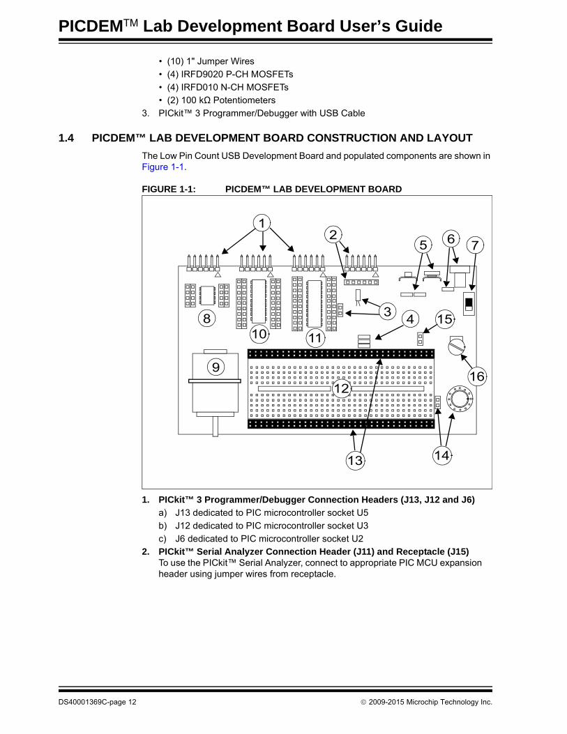
The Low Pin Count USB Development Board and populated components are shown in Figure 1-1.
FIGURE 1-1: PICDEM™ LAB DEVELOPMENT BOARD
1. PICkit™ 3 Programmer/Debugger Connection Headers (J13, J12 and J6)
a) J13 dedicated to PIC microcontroller socket U5
b) J12 dedicated to PIC microcontroller socket U3
c) J6 dedicated to PIC microcontroller socket U2
2. PICkit™ Serial Analyzer Connection Header (J11) and Receptacle (J15)To use the PICkit™ Serial Analyzer, connect to appropriate PIC MCU expansion header using jumper wires from receptacle.
12
34
5 6 7
8
9
10 11
12
13 14
15
16
DS40001369C-page 12 2009-2015 Microchip Technology Inc.

Overview
3. 32 kHz Crystal Oscillator (Y1) and Connection Header (J7)
4. VDD Connect/Disconnect Jumpers (J3, J4, J5)
a) J3 jumper connects/disconnects VDD1 supply to PIC16F690 MCU in socket U2
b) J4 jumper connects/disconnects VDD2 supply to PIC16F819 MCU in socket U3
c) J5 jumper connects/disconnects VDD3 supply to PIC10F206 MCU in socket U5
5. Battery Clip Connection (BT1) for 9V Battery and Jumpers (J14)J14 jumpers connect/disconnect battery terminals for use in future lab on battery chargers.
6. 9 VDC Supply Connector (J1) and Connect/Disconnect Jumper (J2)
7. Power ON Switch (SW1)
8. 8-Pin PDIP PIC10F MCU Socket (U5) and Bilateral Dual-Row Expansion Headers (J10 and J18)Dual-row expansion headers provide connectivity to each pin on the PIC10F206 MCU populating socket U5.
9. 5V Brushed DC Motor
10. 18-Pin PDIP PIC MCU Socket (U3) and Bilateral Dual-Row Expansion Headers (J17 and J16)Dual-row expansion headers provide connectivity to each pin on the PIC16F819 MCU populating socket U3.
11. 8, 14, 20-Pin PDIP PIC MCU Socket (U2) and Bilateral Dual-Row Expansion Headers (J8 and J9)Dual-row expansion headers provide connectivity to each pin on the PIC16F690 MCU populating socket U2.
12. Solderless Prototyping Area
13. Bilateral Dual-Row Supply Headers (J22 and J23) Provide both VDD and VSS connectivity bilaterally to the solderless prototyping area.
14. 0.2 Watt, 8-Ohm Speaker (LS1) with Connection Header (J19)J19 connector used to connect speaker LS1 to user application using jumper wires.
15. Battery Positive (CP+) and Negative (CP-) Connection Header (J26)Provides connectivity of positive and negative battery terminals to the user application using jumper wires.
16. Variable VDD Potentiometer (R1)Potentiometer used to vary PIC MCU supply voltage from approximately 1.3V to approximately 5V.
2009-2015 Microchip Technology Inc. DS40001369C-page 13
PICDEMTM Lab Development Board User’s Guide
1.5 TARGET POWER
The PICDEM™ Lab Development Board can be powered in one of the following ways:
1. Using a 9–12 VDC power supply connected to connector J1 (Microchip part #AC162039 recommended)Ensure that connect/disconnect jumper J2 is in place.
2. Using a 9V battery connected to connector BT1Ensure that connect/disconnect jumpers J14 are in place.
3. A PICkit™ 3 Programmer/Debugger connected to any one of the three PICkit Programmer/Debugger connectors J13, J12 and J6 (recommended for low-power applications only).
When using methods 1 or 2, each PIC microcontroller has an associated connect/disconnect jumper that, when in place, enables the positive supply voltage to the respective VDD pins. The VDD jumpers connect to the following PIC microcontroller sockets:
1. VDD1 (J3) connects/disconnects supply voltage to the PIC microcontroller populating U2.
2. VDD2 (J4) connects/disconnects supply voltage to the PIC microcontroller populating U3.
3. VDD3 (J5) connects/disconnects supply voltage to the PIC microcontroller populating U5.
Using methods 1 or 2 enables the use of the variable VDD potentiometer (R1) to control supply voltages from approximately 1.3 to 5V. Rotating the potentiometer clockwise will raise the supply voltage while rotating the potentiometer counterclockwise will decrease the supply voltage.
1.6 CONNECTING THE PICKIT™ 3 PROGRAMMER/DEBUGGER
The three PIC microcontrollers populating sockets U5, U3 and U2 have their own PICkit Programmer/Debugger (ICSP™) connectors so that each can be programmed or debugged individually. The ICSP connect to the following PIC microcontroller sockets:
1. ICSP1 (J6) connects to the PIC microcontroller populating U2.
2. ICSP2 (J12) connects to the PIC microcontroller populating U3.
3. ICSP3 (J13) connects to the PIC microcontroller populating U5.
The PICkit Programmer/Debugger connects to the ICSP connector as shown in Figure 1-2.
Note: When using the PICkit™ 3 Programmer/Debugger as the power source, the variable VDD potentiometer (R1) will not vary the supply voltage.
DS40001369C-page 14 2009-2015 Microchip Technology Inc.

Overview
FIGURE 1-2: CONNECTING THE PICkit™ 3 PROGRAMMER/DEBUGGER TO AN ICSP™ CONNECTOR
The PICkit™ 3 Programmer/Debugger is then connected to an available USB port on the PC using the included USB cable.
1.7 SOLDERLESS PROTOTYPING AREA STRIP CONFIGURATION
The solderless prototyping area contains a variety of strips under the perforated plastic block. These strips “short” vertical rows of holes together as shown in Figure 1-3.
FIGURE 1-3: SOLDERLESS PROTOTYPING AREA STRIP CONFIGURATION
ICSP™ CONNECTOR
PICkit™ Programmer/Debugger
Denotes Pin 1
Solderless Prototyping Area
Solderless Prototyping Area Showing Strip Connections
2009-2015 Microchip Technology Inc. DS40001369C-page 15

PICDEMTM Lab Development Board User’s Guide
NOTES:
DS40001369C-page 16 2009-2015 Microchip Technology Inc.

PICDEMTM LAB DEVELOPMENT
BOARD USER’S GUIDEChapter 2. Getting Started
2.1 INTRODUCTION
This chapter is intended to prepare the reader to complete the labs in the remainingchapters of this user’s guide.
2.2 PREREQUISITES
The labs contained within this lab manual assumes the user:
1. Has a basic understanding of the C programming language.
2. Understands basic circuit analysis.
2.3 THE SOFTWARE CONTROL LOOP
The labs used in this user’s guide implement a software control loop in variousconfigurations, but always in the same sequence as shown in Example 2-1.
FIGURE 2-1: MAIN() SOFTWARE CONTROL LOOP FLOWCHART FOR USED IN LABS
main()
Loop Forever
Timing()
Initialize()
Get_Inputs()
Decide()
Do_Outputs()
2009-2015 Microchip Technology Inc. DS40001369C-page 17

PICDEMTM Lab Development Board User’s Guide
Each block of the software control loop represents a function that organizes tasks intological, organized groupings that are called from the main function (main()). Noticethe Initialize() is called only once while the remaining functions are executedrepeatedly. This method organizes the embedded firmware application into a logicsequence of events:
1. Initalize():
- Initializes the microcontroller, the peripherals used in the application and any global variables used by multiple functions.
2. Get_Inputs():
- Obtains any input information either on-chip (from internal registers, etc...) or off-chip (pin voltage levels).
3. Decide():
- Makes decisions based on the input information gathered in the previous function to manipulate global variables.
4. Do_Outputs():
- Based on the decisions made in the previous function, this function outputs data onto the pins of the microcontroller or to registers within the device.
5. Timing():
- This function determines how fast the software control loop executes.
Example 2-1 shows a typical main() calling the various functions that make up thesoftware control loop.
EXAMPLE 2-1: TYPICAL SOFTWARE CONTROL LOOP MAIN() USED IN LABS
An infinity loop will be used by all labs in this user’s guide created using a whileloop that repeatedly call the functions within the curly braces as long as there is powerto the microcontroller.
Global variables are used wherever needed in lieu of passing variables betweenfunctions.
void main(void)
Initialize(); //Initialize the relevant registers
while(1)
Decide();//Make any decisions Do_Outputs(); //Perform any outputsTiming();//Sets execution rate of the
//Software Control Loop
DS40001369C-page 18 2009-2015 Microchip Technology Inc.

Getting Started
2.4 MPLAB® X IDE AND XC COMPILER DOWNLOAD INSTRUCTIONS
1. The following steps outline how to download the latest version of the MPLAB® XIDE and XC compiler. It is strongly recommended that all open programs andapplications are closed to expedite the installation process.
2. Using a PC that is connected to the Internet, navigate to the MPLAB X IDEdownload page at the following url: www.microchip.com/mplabx.
3. This page outlines the MPLAB X IDE and also features plug-ins that can bedownloaded, User’s Guides and other useful information.
4. Scroll down to the Downloads section of the page and select the latest fullrelease zip file for MPLAB X IDE vX.XX.
5. When prompted, select Run and the .exe file will download.
FIGURE 2-2: RUN .EXE TO DOWNLOAD FILE
6. Once downloaded, the MPLAB X IDE Installation window should open. ClickNext to proceed with the installation.
7. In the next window, read through the MPLAB X IDE License Agreement andensure that the I accept the terms of the license agreement radio button isselected. Click Next to continue with the installation.
8. In the Installation Directory window it is recommended to use the defaultdirectory. Click Next to continue.
9. In the Select Programs window, choose which MPLAB X programs to install.(Only MPLAB X IDE is required for the labs).
10. Click Next in the Ready to Install window to start the installation (this may takeseveral minutes to complete).
11. After installation is complete, the user will be reminded that the XC compilers arenot installed. It is recommended that the user install the compilers at this point.Check the box and click Finish to continue.
FIGURE 2-3: COMPLETE THE MPLAB® X IDE V2.30 SETUP WIZARD
12. The MPLAB® XC Compilers web page should open. If not, go to:www.microchip.com/mplabxc.
13. This page outlines the MPLAB XC compilers’ features and other usefulinformation.
2009-2015 Microchip Technology Inc. DS40001369C-page 19
PICDEMTM Lab Development Board User’s Guide
14. Scroll down to the Downloads section of the page and select the latest releasefile for MPLAB XC Compiler vX.XX.
15. Click Run to download and run the .exe file.
FIGURE 2-4: RUN AND DOWNLOAD .exe FILE
16. Click Next in the MPLAB XC Compiler setup window.
17. In the next window, read through the License Agreement and ensure that the Iaccept the terms of the license agreement radio button is selected. Click Nextto continue with the installation.
18. Select the Install compiler radio button in the Choose Installer window. ClickNext.
19. Ensure the “Configure MPLAB XC8 Compiler as a network client” box isunchecked and click Next.
20. In the Installation Directory window it is recommended to use the defaultdirectory. Click Next to continue.
21. In the Compiler Settings window, ensure all boxes are checked.
22. Click Next in the Ready to Install window.
23. In the Licensing Information window, click Next.
24. Click Finish to finish installation.
2.5 INSTALLING THE INCLUDED LAB FILES
The PICDEM™ Lab Development Kit product pagehttp://www.microchip.com/DevelopmentTools/ProductDetails.aspx?PartNO=dm163045has a .zip file called PICDEM Lab Development Kit Lab Directory andSolutions under Documents. This file provides a location for the user to save any
projects created while completing the labs in this user's guide and contains solutions foreach lab in a folder labeled solution. To install this folder, simply extract the contents of
the .zip file to the C:\ directory.
Note: Lab folders must be installed to C:\ to be used by the MPLAB® X IDE.
DS40001369C-page 20 2009-2015 Microchip Technology Inc.

PICDEMTM LAB DEVELOPMENT
BOARD USER’S GUIDEChapter 3. General Purpose Input/Output Labs
3.1 INTRODUCTION
The following labs cover some of the fundamental features of the General PurposeInput/Output (GPIO) peripherals available on the PIC16F690. As the name implies,these peripherals are used for general purpose applications that can monitor andcontrol other off-chip devices. Some PIC® microcontrollers have multiple GPIOperipherals on-chip including the PIC16F690 used in the following labs. Therefore, thePORTx naming convention is used. Available ports on the PIC16F690 are:
• PORTA
• PORTB
• PORTC
Reading through the data sheet highlights some of the unique characteristicsassociated with each port and the reader is encouraged to explore these in greaterdetail once comfortable with the labs in this user’s guide. The labs will focus on two ofthe port peripherals: PORTC and PORTA. Labs will be naturally divided into twosections since these are General Purpose Input/Output peripherals:
• Output Labs
• Input Labs
Output labs will introduce the reader to concepts necessary to configuring theseperipherals for output to off-chip devices using applicable registers by lighting eightLEDs connected to the PORTC pins
The Input labs will then add a push button interfacing to one of the PORTA pins tohighlight concepts necessary for configuring these peripherals to receive informationfrom off-chip devices. Finally, interrupts will be used to optimize the application fordifferent purposes.
3.2 GENERAL PURPOSE INPUT/OUTPUT LABS
• Output Labs:
- Lab 1: Light LEDs
- Lab 2: Flash LEDs (Delay Loop)
- Lab 3: Simple Delays Using Timer0
- Lab 4: Rotate LEDs
• Input Labs:
- Lab 5: Adding a Push Button
- Lab 6: Push Button Interrupt
- Lab 7: Push Button Interrupt-on-Change
- Lab 8: Using Weak Pull-ups
2009-2015 Microchip Technology Inc. DS40001369C-page 21
PICDEMTM Lab Development Board User’s Guide
3.3 GPIO OUTPUT LABS
3.3.1 Reference Documentation
All documentation on the PICDEM™ Lab Development Kit is available on the product’spage at www.microchip.com.
• PIC16F690 Data Sheet (DS41262)
- Section 2.2.2.2: Option Register
- Section 2.2.2.3: Interrupt Control Register INTCON
- Section 4: I/O Ports
- Section 5: Timer0 Module
• Timers: Timer0 Tutorial (Part 1) (DS51682)
• Timers: Timer0 Tutorial (Part 2) (DS51702)
3.3.2 Equipment Required for GPIO Output Labs
To complete the labs in this section, the following components are required:
1. 8 – Light Emitting Diodes
2. 8 – 470 resistors
3. PIC16F690 populating socket U2
4. Assorted jumper wires
3.3.3 PICDEM Lab Development Board Setup for GPIO Output Labs
The GPIO output labs will require that the PICDEM Lab Development Board beconfigured as shown in Figure 3-1 using the components listed in the previous section.
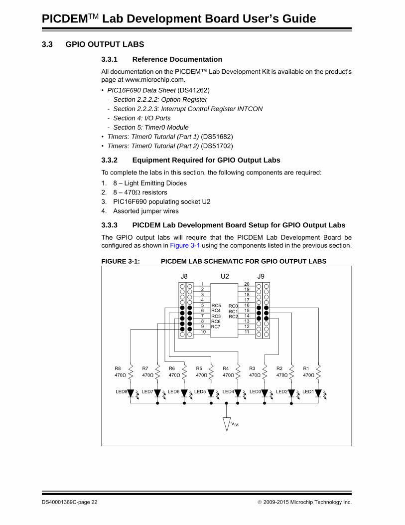
FIGURE 3-1: PICDEM LAB SCHEMATIC FOR GPIO OUTPUT LABS
U212345678910
20191817161514131211
RC0RC1RC2RC3
RC4RC5
RC6RC7
J9J8
R8
470Ω
R4
470Ω
R7
470Ω
R6
470Ω
R5
470Ω
R3
470Ω
R2
470Ω
R1
470Ω
LED8 LED7 LED6 LED4 LED3 LED2 LED1LED5
VSS
DS40001369C-page 22 2009-2015 Microchip Technology Inc.

General Purpose Input/Output Labs
Special care should be observed when connecting the LED jumper wires to theexpansion headers surrounding the PIC16F690, as the PORTC pins are not insequential order. The 470resistors are used to limit the current across the LEDs tomanufacturer specifications. Furthermore, the PIC16F690 Data Sheet electricalspecifications (see Section 17.0) stipulate that each port pin should not source/sinkmore than 25 mA. The maximum output current sourced/sunk by all port pins combinedshould not exceed 200 mA. The 470 resistors keep all source current well withinthese specifications.
3.3.4 Lab 1: Light LEDs
3.3.4.1 NEW REGISTERS USED IN THIS LAB
To configure the peripherals used in this lab, the following registers are used:
1. PORTC Register: PORTC (Register 4-11 in Section 4 of the PIC16F690 DataSheet).
- 8-bit bidirectional port.
2. PORTC Tri-State Register: TRISC (Register 4-12 in Section 4 of the PIC16F690Data Sheet).
- Configures corresponding bits in PORTC as either input or output.
3. Analog Select Register High and Analog Select Register Low: ANSELH andANSEL (Registers 4-4 and 4-3 in Section 4 of the PIC16F690 Data Sheet).
- Configure associated pins for analog or digital input signals.
3.3.4.2 OVERVIEW
This first lab demonstrates how to output data from the PORTC peripheral on thePIC16F690 to its associated pins. LEDs connected to PORTC pins will light when theassociated pin is driven high (approx. VDD) or turn the LED OFF when driven low(approx. VSS). The port peripherals will all default to input on start-up and will thereforeneed to be configured as output using the TRISC register. Also, PORTC pins RC0,RC1, RC2, RC3, RC6 and RC7 are configurable for both analog and digital signals. Onstart-up, any analog/digital functional pin is defaulted to analog. Therefore, thisapplication will require that these pins be configured as digital by configuring theassociated bits in the ANSEL and ANSELH analog select registers.
FIGURE 3-2: MAIN() SOFTWARE CONTROL LOOP FLOWCHART FOR LAB 1
main()
Initialize()
Do_Outputs()
Loop Forever
2009-2015 Microchip Technology Inc. DS40001369C-page 23

PICDEMTM Lab Development Board User’s Guide
Figure 3-2 shows the software control loop that will be implemented in this lab. At device power-up, the first functional block called from the main() is Initialize(). This function will initialize the PORTC peripheral as follows:
• Clear the PORTC register data
• Configure the ANSEL and ANSELH bits so that all associated PORTC pins are digital
• Configure the associated PORTC pins as all output using the TRISC register
The next function called from main() is Do_Outputs(). This function will assignvalues to the PORTC register that will drive the associated pins high or low to light theLEDs connected.
3.3.4.3 PROCEDURE
The following steps will demonstrate how to create a new project in MPLAB® IDE.
1. Open MPLAB X IDE by selecting Start > Program Files > Microchip > MPLAB XIDE > MPLAB X IDE vX.XX.
2. In the MPLAB X IDE Toolbar, select File >New Project.
FIGURE 3-3: NEW MPLAB IDE PROJECT SELECTION
Note: The PORT register should always be initialized to a known value before configuring the associated TRIS bit. This avoids unexpected voltage levels on the associated pins since at start-up port bit values are unknown.
DS40001369C-page 24 2009-2015 Microchip Technology Inc.
General Purpose Input/Output Labs
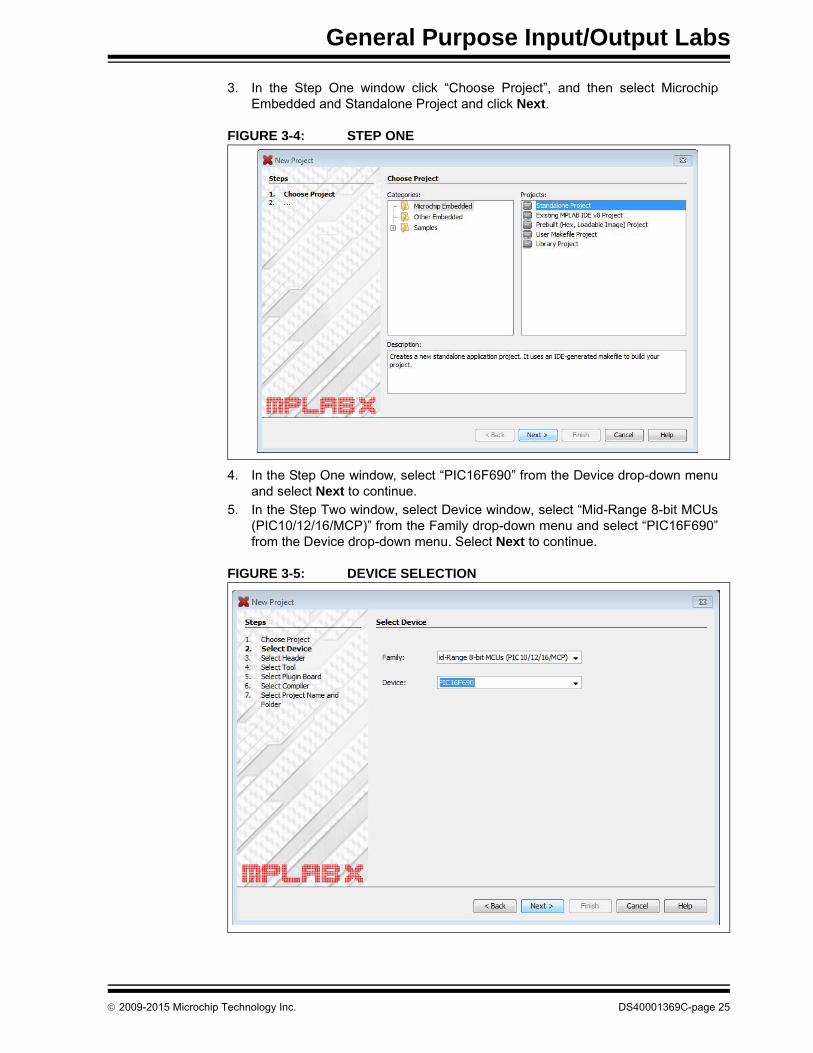
3. In the Step One window click “Choose Project”, and then select MicrochipEmbedded and Standalone Project and click Next.
FIGURE 3-4: STEP ONE
4. In the Step One window, select “PIC16F690” from the Device drop-down menuand select Next to continue.
5. In the Step Two window, select Device window, select “Mid-Range 8-bit MCUs(PIC10/12/16/MCP)” from the Family drop-down menu and select “PIC16F690”from the Device drop-down menu. Select Next to continue.
FIGURE 3-5: DEVICE SELECTION
2009-2015 Microchip Technology Inc. DS40001369C-page 25

PICDEMTM Lab Development Board User’s Guide
6. In the Select Header window, select None from the Supported Debug Headerdrop-down menu and select Next to continue.
FIGURE 3-6: HEADER SELECTION
7. In the Select Tool window, select “PICkit3” and click Next to continue.
FIGURE 3-7: TOOL SELECTION
DS40001369C-page 26 2009-2015 Microchip Technology Inc.

General Purpose Input/Output Labs
8. In the Select Compiler window, select “XC8 (vX.XX)” and click Next to continue.
FIGURE 3-8: COMPILER SELECTION
9. In the Select Project Name and Folder window, type a name for the project into“Project Name”. It is recommended to use the default location for “ProjectLocation” and “Project Folder”. Choose the option “Set as main project” andselect Finish to continue.
FIGURE 3-9: SELECT PROJECT NAME AND FOLDER
2009-2015 Microchip Technology Inc. DS40001369C-page 27

PICDEMTM Lab Development Board User’s Guide
10. In the left pane of the MPLAB X window under the Projects tab, right-click on“Source Files” and select “Add Existing Item”.
FIGURE 3-10: SELECT PROJECT SOURCE
11. Browse to the GPIO_Lab1.c file, select it and click Select to add it to the project. Then double click GPIO_Lab1.c to open the file.
12. The MPLAB® IDE workspace should now be open. If the Project window is not visible, it can be opened by selecting View > Project.
DS40001369C-page 28 2009-2015 Microchip Technology Inc.

General Purpose Input/Output Labs
FIGURE 3-11: PROJECT WINDOW
13. Double click on the GPIO_Lab1.c source file in the Project window to open.
14. Copy/paste the code in Example 3-1 into the Initialize() section labeled://ADD INITIALIZE CODE HERE.
EXAMPLE 3-1: INITIALIZE() CODE FOR LAB 1
//Clear PORTC to a known statePORTC = 0b00000000;
//Configure PORTC's ANALOG/DIGITAL pins as all DigitalANS4 = 0;//Associated with RC0ANS5 = 0;//Associated with RC1ANS6 = 0;//Associated with RC2ANS7 = 0;//Associated with RC3ANS8 = 0;//Associated with RC6ANS9 = 0;//Associated with RC7
//Configure PORTC pins as all output//i.e. 1 = Input, 0 = OutputTRISC0 = 0;//Make RC0 (pin 16) outputTRISC1 = 0;//Make RC1 (pin 15) outputTRISC2 = 0;//Make RC2 (pin 14) outputTRISC3 = 0;//Make RC3 (pin 7) outputTRISC4 = 0;//Make RC4 (pin 6) outputTRISC5 = 0;//Make RC5 (pin 5) outputTRISC6 = 0;//Make RC6 (pin 8) outputTRISC7 = 0;//Make RC7 (pin 9) output
2009-2015 Microchip Technology Inc. DS40001369C-page 29
PICDEMTM Lab Development Board User’s Guide
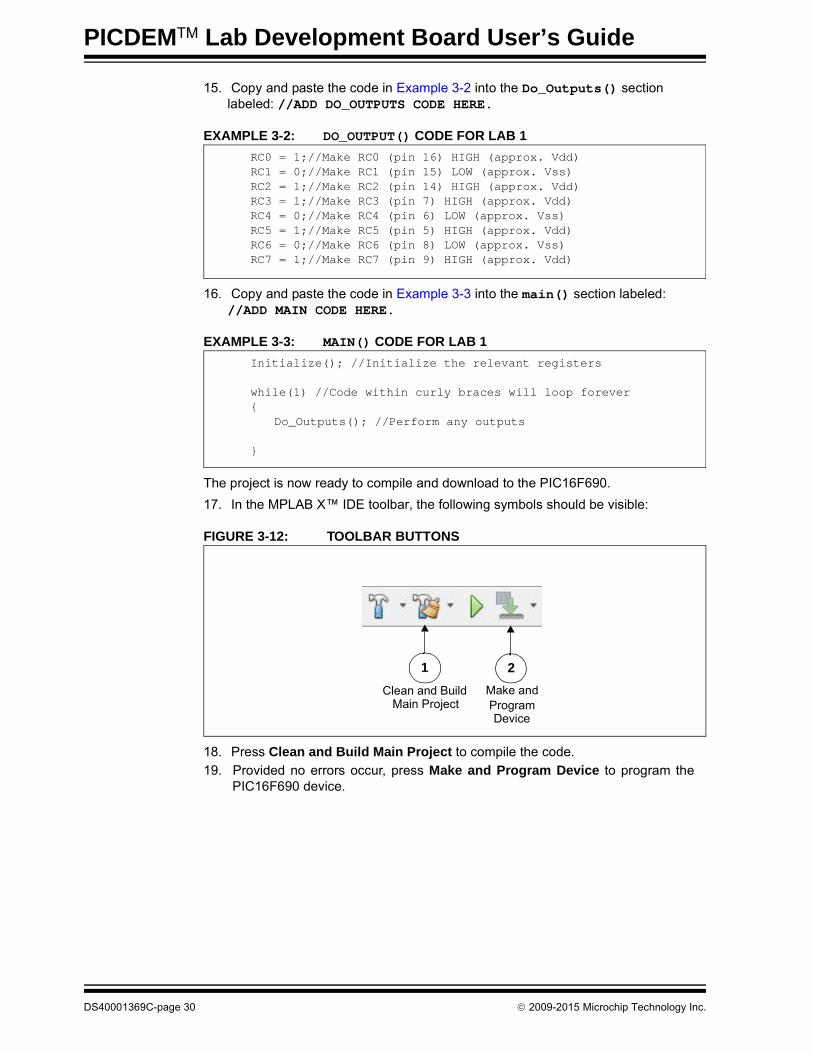
15. Copy and paste the code in Example 3-2 into the Do_Outputs() section labeled: //ADD DO_OUTPUTS CODE HERE.
EXAMPLE 3-2: DO_OUTPUT() CODE FOR LAB 1
16. Copy and paste the code in Example 3-3 into the main() section labeled://ADD MAIN CODE HERE.
EXAMPLE 3-3: MAIN() CODE FOR LAB 1
The project is now ready to compile and download to the PIC16F690.
17. In the MPLAB X™ IDE toolbar, the following symbols should be visible:
FIGURE 3-12: TOOLBAR BUTTONS
18. Press Clean and Build Main Project to compile the code.
19. Provided no errors occur, press Make and Program Device to program thePIC16F690 device.
RC0 = 1;//Make RC0 (pin 16) HIGH (approx. Vdd)RC1 = 0;//Make RC1 (pin 15) LOW (approx. Vss)RC2 = 1;//Make RC2 (pin 14) HIGH (approx. Vdd)RC3 = 1;//Make RC3 (pin 7) HIGH (approx. Vdd)RC4 = 0;//Make RC4 (pin 6) LOW (approx. Vss)RC5 = 1;//Make RC5 (pin 5) HIGH (approx. Vdd)RC6 = 0;//Make RC6 (pin 8) LOW (approx. Vss)RC7 = 1;//Make RC7 (pin 9) HIGH (approx. Vdd)
Initialize(); //Initialize the relevant registers
while(1) //Code within curly braces will loop forever
Do_Outputs(); //Perform any outputs
21
Clean and Build Main Project
Make and Program Device
DS40001369C-page 30 2009-2015 Microchip Technology Inc.
General Purpose Input/Output Labs
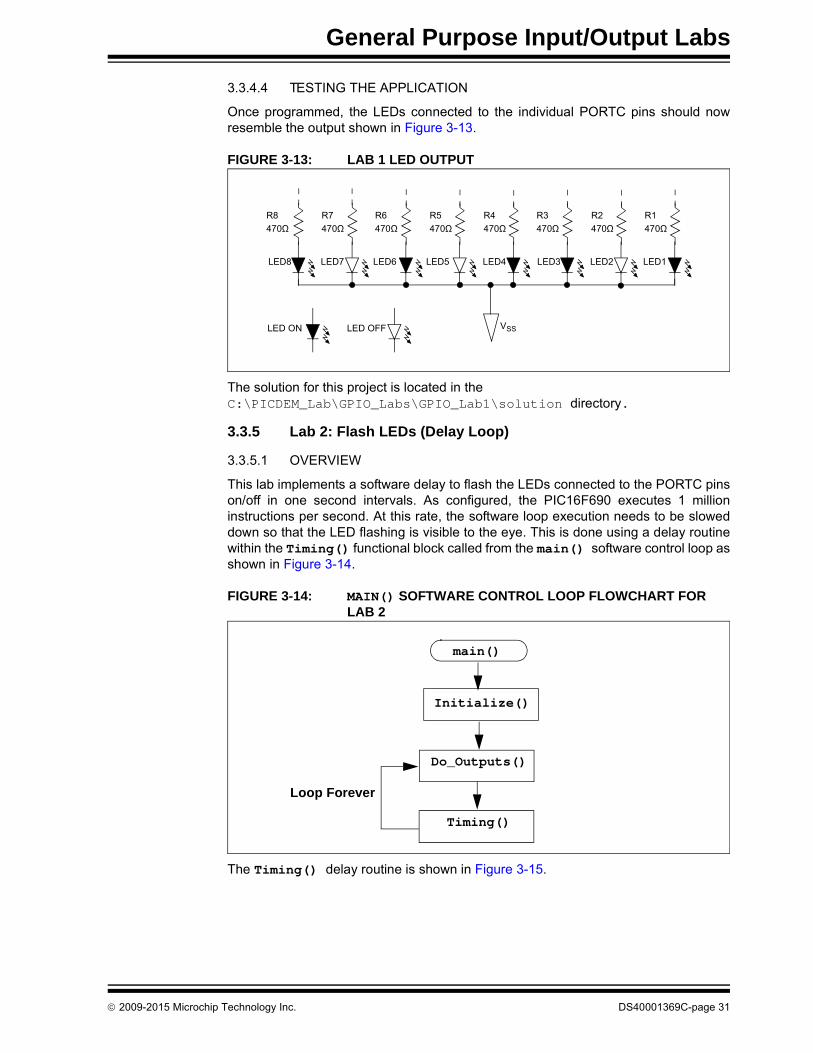
3.3.4.4 TESTING THE APPLICATION
Once programmed, the LEDs connected to the individual PORTC pins should nowresemble the output shown in Figure 3-13.
FIGURE 3-13: LAB 1 LED OUTPUT
The solution for this project is located in the C:\PICDEM_Lab\GPIO_Labs\GPIO_Lab1\solution directory.
3.3.5 Lab 2: Flash LEDs (Delay Loop)
3.3.5.1 OVERVIEW
This lab implements a software delay to flash the LEDs connected to the PORTC pinson/off in one second intervals. As configured, the PIC16F690 executes 1 millioninstructions per second. At this rate, the software loop execution needs to be sloweddown so that the LED flashing is visible to the eye. This is done using a delay routinewithin the Timing() functional block called from the main() software control loop asshown in Figure 3-14.
FIGURE 3-14: MAIN() SOFTWARE CONTROL LOOP FLOWCHART FOR LAB 2
The Timing() delay routine is shown in Figure 3-15.
R8
470Ω
R4
470Ω
R7
470Ω
R6
470Ω
R5
470Ω
R3
470Ω
R2
470Ω
R1
470Ω
LED8 LED7 LED6 LED4 LED3 LED2 LED1LED5
VSSLED ON LED OFF
main()
Initialize()
Do_Outputs()
Loop Forever
Timing()
2009-2015 Microchip Technology Inc. DS40001369C-page 31

PICDEMTM Lab Development Board User’s Guide
FIGURE 3-15: TIMING() DELAY ROUTINE FLOWCHART FOR LAB 2
Two variables are used, delay_var1 and delay_var2. The delay_var2 isdecremented by 1 each time delay_var1 is decremented from 45571 to 0. Thesevalues have been determined through trial and error using a test procedure detailed inthe “Timers: Timer0 Tutorial (Part 1)” (DS51682) included on the PICDEM™ LabDevelopment Kit CD. This delay ties up the processor for one second when using the4 MHz internal oscillator.
The Initialize() configures the PORTC as follows:
• PORTC
- Set all bits in the PORTC register HIGH
- Configure all PORTC pins as digital outputs
The Do_Outputs() changes somewhat from the previous lab by implementing theXOR operator to toggle the value in each PORTC bit location each time through thesoftware loop. The XOR operator is implemented in code as follows:RCx ^= 1; This translates to: “Make RCx equal to the current value in RCx XOR’d with 1”
When a value is XOR’d with itself, the result is ‘0’ (i.e., 1 XOR’d with 1 = 0, 0 XOR’dwith 0 = 0). When a value is XOR’d with a value different than itself, the result is ‘1’ (i.e.,1 XOR’d with 0 = 1). Therefore, each time through the loop PORTC bits will toggle from1-to-0 or 0-to-1, depending on its current value.
3.3.5.2 PROCEDURE
Using the code developed in the previous lab, make the following changes:
1. Copy and paste the code in Example 3-4 over the Initialize() code from theprevious lab.
TIMING()
Create two 8-bit variables:
• delay_var1 = 45571• delay_var2 = 3
delay_var2 - 1 = 0
?
delay_var1 - 1 = 0
?
END
delay_var1 = 45571
YES
YES
NO
NO
Note: The reader may wish to create a new project as per the previous lab called GPIO_Lab2.mcp
DS40001369C-page 32 2009-2015 Microchip Technology Inc.
General Purpose Input/Output Labs
EXAMPLE 3-4: INITIALIZE() CODE FOR LAB 2
The only change from the previous lab is that the PORTC bits are all set high to 1.
2. Copy and paste the code in Example 3-5 over the Do_Outputs() code from theprevious lab to accommodate the XOR bit toggle.
EXAMPLE 3-5: DO_OUTPUT() CODE FOR LAB 2
3. Copy and paste the code in Example 3-6 into the Timing() section labeled://ADD TIMING CODE HERE
//Set all PORTC bits HIGH (to a known state)PORTC = 0b11111111;
//Configure PORTC's ANALOG/DIGITAL pins as all DigitalANS4 = 0;//Associated with RC0ANS5 = 0;//Associated with RC1ANS6 = 0;//Associated with RC2ANS7 = 0;//Associated with RC3ANS8 = 0;//Associated with RC6ANS9 = 0;//Associated with RC7
//Configure PORTC pins as all output//i.e. 1 = Input, 0 = OutputTRISC0 = 0;//Make RC0 (pin 16) outputTRISC1 = 0;//Make RC1 (pin 15) outputTRISC2 = 0;//Make RC2 (pin 14) outputTRISC3 = 0;//Make RC3 (pin 7) outputTRISC4 = 0;//Make RC4 (pin 6) outputTRISC5 = 0;//Make RC5 (pin 5) outputTRISC6 = 0;//Make RC6 (pin 8) outputTRISC7 = 0;//Make RC7 (pin 9) output
RC0 ^= 1;//XOR current RC0 value with 1RC1 ^= 1;//XOR current RC1 value with 1RC2 ^= 1;//XOR current RC2 value with 1RC3 ^= 1;//XOR current RC3 value with 1RC4 ^= 1;//XOR current RC4 value with 1RC5 ^= 1;//XOR current RC5 value with 1RC6 ^= 1;//XOR current RC6 value with 1RC7 ^= 1;//XOR current RC7 value with 1
2009-2015 Microchip Technology Inc. DS40001369C-page 33
PICDEMTM Lab Development Board User’s Guide
EXAMPLE 3-6: TIMING() FOR LAB 2
4. Copy and paste the code in Example 3-7 over the main() code from theprevious lab to incorporate the Timing().
EXAMPLE 3-7: MAIN() CODE FOR LAB 2
Compile the project. There should be no errors.
3.3.5.3 TESTING THE APPLICATION
Program the PIC16F690. The LEDs connected to the individual PORTC pins shouldnow all flash on/off in 1-second intervals.
The solution for this project is located in theC:\PICDEM_Lab\GPIO_Labs\GPIO_Lab2\solution directory.
3.3.6 Lab 3: Simple Delays Using Timer0
3.3.6.1 NEW REGISTERS USED IN THIS LAB
To configure the peripherals used in this lab, the following registers are used:
1. Timer0 Module Register: TMR0
- Holds a count value of the number of selected edge transition of a clocksource.
2. OPTION Register: OPTION_REG (Register 5-1 in Section 5 of the PIC16F690Data Sheet).
- Selects clock source used to increment TMR0 result register.
- Selects clock source edge transition to increment TMR0.
3. Software configurable prescaler to determine the number of clock source edgetransitions before incrementing TMR0 register value.
//--------DELAY 1second-------------------------//Variable used in delay loopunsigned int delay_var1 = 45571;unsigned char delay_var2 = 3;//Nested while loops to implement a 1 second delay//Decrement delay_var2, if 0 jump out of loopwhile(--delay_var2)
//Decrement delay_var1, if 0 jump out of loopwhile(--delay_var1);
Initialize(); //Initialize the relevant registers
while(1)
Do_Outputs(); //Perform any outputs
Timing();//Sets execution rate of the//Software Control Loop
DS40001369C-page 34 2009-2015 Microchip Technology Inc.

General Purpose Input/Output Labs
4. Interrupt Control Register: INTCON (Register 2-3 in Section 2 of the PIC16F690Data Sheet).
- Contains a flag that when 1, indicates a TMR0 register overflow has occurred.
3.3.6.2 OVERVIEW
To implement a more accurate delay, the Timer0 peripheral can be used. Timer0 is an8-bit timer/counter that uses a clock source to increment an 8-bit register called TMR0.Since this register is 8 bits, it can increment up 28 = 256 times or 010 - 25510(000000002 - 111111112) inclusive then rollover or overflow back to ‘0’. WheneverTMR0 overflows, a Timer0 Overflow Flag (T0IF) in the ITCON register is set to ‘1’. TheOPTION register also features a prescaler that determines how many clock sourcecycles it takes to increment TMR0 by ‘1’. In this way, simply by tracking the T0IF, veryaccurate delays can be implemented. In this lab, the TMR0 register is configured toincrement on the low-to-high transition of an available internal instruction clock on thePIC16F690. This internal instruction clock runs at the rate of the internal oscillatorfrequency FOSC divided by 4. Therefore, when the PIC16F690 is configured to operateusing the internal 4 MHz oscillator, this internal instruction clock runs at a rate of FOSC/4 = 4MHz/4 = 1MHz. This is a period of 1/1MHz = 1 S. If it is known that TMR0increments every 1 S, and it takes 256 internal instruction clock cycles to cause aTMR0 overflow (i.e., 0-255 inclusive), then Equation 3-1 can be derived:
EQUATION 3-1: TMR0 OVERFLOW PERIOD USING FOSC/4
As mentioned, Timer0 also features a prescaler that can be configured to increment thevalue in TMR0 every 2, 4, 8, 16, 32, 64, 128, or 256 clock source transitions. Therefore,this feature can be added to Equation 3-1 to create Equation 3-2.
EQUATION 3-2: TMR0 OVERFLOW PERIOD WHEN INCLUDING THE PRESCALER
Finally, TMR0 is a writable register. Meaning that a value can be added to the registerto offset the number of counts it takes for the overflow to occur. Equation 3-3demonstrates how to calculate the value to preload the TMR0 register with to create a10 mS overflow period.
TMR0 Overflow Period = (4/FOSC) x 256 = 1 Second x 256 = 256 Seconds
TMR0 Overflow Period = (4/FOSC) x 256 x prescaler
Using a 1:32 prescaler setting as an example and a 4 MHz internal oscillator
TMR0 Overflow Period = 1 S x 256 x 32 = 8.192mS
2009-2015 Microchip Technology Inc. DS40001369C-page 35

PICDEMTM Lab Development Board User’s Guide
EQUATION 3-3: CALCULATING A TMR0 PRELOAD VALUE TO GENERATE A 10MS OVERFLOW PERIOD
The software flowchart to implement a 10 mS delay is shown in Figure 3-16.
FIGURE 3-16: DELAY_10MS() USING TIMER0
The maximum overflow period that can be achieved using Timer0 only utilizes a 1:256prescaler is as shown in Equation 3-4.
EQUATION 3-4: MAXIMUM TMR0 OVERFLOW PERIOD
Desired TMR0 Overflow Period = (4/FOSC) x (256 - Preload Value) x prescaler
Using a 1:64 prescaler setting, a 4 MHz internal oscillator and requiring a 10 mS overflow period:
10mS = 1 Second x (256 - Preload Value) x 64
10mS/(1 Second x 64) = 256 - Preload Value
Preload Value = 256 - [10mS/(1 Second x 64)]
Preload Value = 99.75 rounded up becomes 100
Note: Therefore, to produce a 10 mS overflow period, using the internal instruction clock with a 4 MHz internal oscillator and a TMR0 prescaler value of 1:64 requires that TMR0 be preloaded with a value of 100.
Delay_10mS()
END
YES
NO
Preload TMR0 register with 100
Clear the TMR0 overflow flag
(T0IF)
T0IF = 0?
TMR0 Overflow Period = (4/FOSC) x 256 x prescaler
using a maximum prescaler setting of 1:256 and the 4 MHz internal oscillator
TMR0 Overflow Period = 1 S x 256 x 256 = 65.5mS
DS40001369C-page 36 2009-2015 Microchip Technology Inc.
General Purpose Input/Output Labs
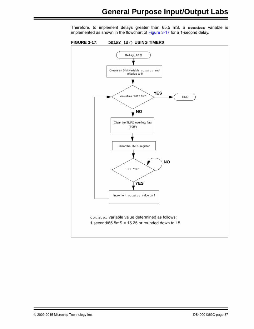
Therefore, to implement delays greater than 65.5 mS, a counter variable isimplemented as shown in the flowchart of Figure 3-17 for a 1-second delay.
FIGURE 3-17: DELAY_1S() USING TIMER0
Delay_1S()
END
YES
NO
counter variable value determined as follows:
1 second/65.5mS = 15.25 or rounded down to 15
Create an 8-bit variable counter and initialize to 0
Clear the TMR0 register
Clear the TMR0 overflow flag
(T0IF)
T0IF = 0?
counter < or = 15?
Increment counter value by 1
NO
YES
2009-2015 Microchip Technology Inc. DS40001369C-page 37

PICDEMTM Lab Development Board User’s Guide
The Initialize() now configures the PIC16F690 peripherals as follows:
• PORTC
- Set all bits in PORTC high
- Make all PORTC pins digital output
• Timer0
- Use the internal instruction clock (FOSC/4) as the TMR0 register clock source
- Increment TMR0 register on low-to-high transition of FOSC/4
- Assign the prescaler to Timer0 and configure to increment on every 256thtransition of FOSC/4
3.3.6.3 PROCEDURE
Using the firmware developed in the previous lab, make the following changes:
1. Copy and paste the code in Example 3-8 at the top of the main firmware sourcefile under the heading labeled:/**SUPPORT ROUTINES**********************************/
EXAMPLE 3-8: DELAY_1S() CODE FOR LAB 3
2. Copy and paste the code in Example 3-9 into the Initialize() over the codefrom the previous lab.
/*---------------------------------------------------------Subroutine: Delay_1SParameters: noneReturns:nothingSynopsis:Creates a 1S delay when called
---------------------------------------------------------*/void Delay_1S(void)
//Create an 8-bit variable called counter//and initialize it to 0unsigned char counter = 0;
while(counter <= 15)//Make sure the T0IF is clearedT0IF = 0;
//Clear the TMR0 registerTMR0 = 0;//Sit here and wait for Timer0 to overflow
while (T0IF == 0);++counter;
DS40001369C-page 38 2009-2015 Microchip Technology Inc.
General Purpose Input/Output Labs
EXAMPLE 3-9: INITIALIZE() CODE FOR LAB 3
3. Finally, copy and paste the code in Example 3-10 into the Timing() over thecode from the previous lab
EXAMPLE 3-10: TIMING() CODE FOR LAB 3
4. The remaining code from the previous lab remains the same. Compile theproject. There should be no errors.
3.3.6.4 TESTING THE APPLICATION
Program the PIC16F690. The application should behave exactly as it did in theprevious lab. Using an oscilloscope to test individual PORTC pin level transitions wouldbe useful to analyze the accuracy of the delay.
The solution for this project is located in the C:\PICDEM_Lab\GPIO_Labs\GPIO_Lab3\solution directory.
//Set all PORTC bits HIGH (to a known state)PORTC = 0b11111111;
//Configure PORTC's ANALOG/DIGITAL pins as all DigitalANS4 = 0;//Associated with RC0ANS5 = 0;//Associated with RC1ANS6 = 0;//Associated with RC2ANS7 = 0;//Associated with RC3ANS8 = 0;//Associated with RC6ANS9 = 0;//Associated with RC7
//Configure PORTC pins as all output//i.e. 1 = Input, 0 = OutputTRISC0 = 0;//Make RC0 (pin 16) outputTRISC1 = 0;//Make RC1 (pin 15) outputTRISC2 = 0;//Make RC2 (pin 14) outputTRISC3 = 0;//Make RC3 (pin 7) outputTRISC4 = 0;//Make RC4 (pin 6) outputTRISC5 = 0;//Make RC5 (pin 5) outputTRISC6 = 0;//Make RC6 (pin 8) outputTRISC7 = 0;//Make RC7 (pin 9) output
//Configure Timer0 as follows:T0CS = 0; //Use the internal instruction clock
//FOSC/4 as the clock sourceT0SE = 0;//Increment TMR0 on low-to-high
//FOSC/4 transitionPSA = 0;//Assign the prescaler to
//Timer0
//Configure Timer0 prescaler to increment//TMR0 every 256 FOSC/4 clock transitionsPS0 = 1;PS1 = 1;PS2 = 1;
Delay_1S(); //Call the 1 second delay
Note: More in-depth tutorials on the Timer0 peripheral are covered in “Timers: Timer0 Tutorial (Part 1)” (DS5162) and “Timers: Timer0 Tutorial (Part 2)” (DS51702) files included on the PICDEM™ Lab Development Kit CD.
2009-2015 Microchip Technology Inc. DS40001369C-page 39

PICDEMTM Lab Development Board User’s Guide
3.3.7 Lab 4: Rotate LEDs
3.3.7.1 OVERVIEW
This lab shifts a high bit in the PORTC register from right-to-left each time through thesoftware loop sequentially lighting the LEDs connected to the PORTC pins in 1-secondintervals as dictated by the Timing(). This lab adds some new functional blocks tothe main() software control loop as shown in Figure 3-18.
FIGURE 3-18: MAIN() SOFTWARE CONTROL LOOP FLOWCHART FOR LAB 4
The addition of an 8-bit global variable (can be manipulated by any function) calledLED_Output is used. This variable will be acted upon by the new Decide() byshifting a high bit in LED_Output from right-to-left each time this function is called. Theflowchart for the Decide() is shown in Figure 3-19.
FIGURE 3-19: DECIDE() FLOWCHART FOR LAB 4
main()
Initialize()
Do_Outputs()
Loop Forever
Timing()
Decide()
Global Variables:
• 8-bit LED_Output
Decide()
LED_Output = 0b10000000
or
LED_Output = 0b00000000
?
END
Shift contents of LED_Output variable left by 1 bit position
YES
NO
LED_Output = 0b00000001
LED_Output variable initialize to 0b00000001 in Initialize()
DS40001369C-page 40 2009-2015 Microchip Technology Inc.

General Purpose Input/Output Labs
The Decide() first checks the current value in LED_Output for two specificconditions:
• Is the Most Significant bit ‘1’? This means that on the next shift, the contents willbe all ‘0’s.
• Is the value currently a ‘0’?
If either condition exists, the function re-initializes LED_Output to set the LeastSignificant bit. Otherwise, there will be a period when none of the LEDs are lit.
The shift is implemented in code as follows:
LED_Output <<= 1;
This translates to: “LED_Output is equal to the current contents of LED_Outputshifted to the left by 1 bit position”
Conversely, to shift the bit to the right the code would be as follows:
LED_Output >>= 1;
The Do_Outputs() will then assign the contents of the LED_Output variable to thePORTC register and whichever bit is high will light the connected LED. (SeeFigure 3-20.)
FIGURE 3-20: RESULTS OF DO_OUTPUT()
The Initialize() now configures the PIC16F690 peripherals as follows:
• PORTC
- Initialize PORTC so that the seven Most Significant bits are ‘0’ and the LeastSignificant bit is ‘1’
- Make all PORTC pins digital output
• Timer0
- Use the internal instruction clock (FOSC/4) as the TMR0 register clock source
- Increment TMR0 register on low-to-high transition of FOSC/4
- Assign the prescaler to Timer0 and configure to increment on every 256thtransition of FOSC/4
• Initialize the LED_Output variable to ‘0’
Do_Outputs() assigns LED_Out-put to PORTC
LED_Output variable
1000000 0 1000000 0PORTC
Do_Outputs() assigns LED_Out-put to PORTC
0100000 0 0100000 0LED_Output variable PORTC
Decide() shifts contents of LED_Output Left by 1 bit position
Corresponding LED lights
Corresponding LED lights
First time through main():
Next time through main():
Initialize() determines initial contents of LED_Output
2009-2015 Microchip Technology Inc. DS40001369C-page 41
PICDEMTM Lab Development Board User’s Guide
3.3.7.2 PROCEDURE
Using the code developed in the previous lab, make the following changes:
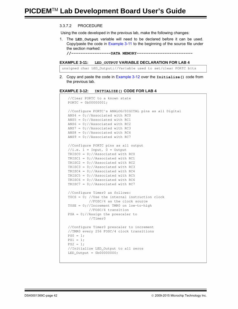
1. The LED_Output variable will need to be declared before it can be used.Copy/paste the code in Example 3-11 to the beginning of the source file underthe section marked://-----------------DATA MEMORY------------------------
EXAMPLE 3-11: LED_OUTPUT VARIABLE DECLARATION FOR LAB 4
2. Copy and paste the code in Example 3-12 over the Initialize() code fromthe previous lab.
EXAMPLE 3-12: INITIALIZE() CODE FOR LAB 4
unsigned char LED_Output;//Variable used to set/clear PORTC bits
//Clear PORTC to a known statePORTC = 0b00000001;
//Configure PORTC's ANALOG/DIGITAL pins as all DigitalANS4 = 0;//Associated with RC0ANS5 = 0;//Associated with RC1ANS6 = 0;//Associated with RC2ANS7 = 0;//Associated with RC3ANS8 = 0;//Associated with RC6ANS9 = 0;//Associated with RC7
//Configure PORTC pins as all output//i.e. 1 = Input, 0 = OutputTRISC0 = 0;//Associated with RC0TRISC1 = 0;//Associated with RC1TRISC2 = 0;//Associated with RC2TRISC3 = 0;//Associated with RC3TRISC4 = 0;//Associated with RC4TRISC5 = 0;//Associated with RC5TRISC6 = 0;//Associated with RC6TRISC7 = 0;//Associated with RC7
//Configure Timer0 as follows:T0CS = 0; //Use the internal instruction clock
//FOSC/4 as the clock sourceT0SE = 0;//Increment TMR0 on low-to-high
//FOSC/4 transitionPSA = 0;//Assign the prescaler to
//Timer0
//Configure Timer0 prescaler to increment//TMR0 every 256 FOSC/4 clock transitionsPS0 = 1;PS1 = 1;PS2 = 1;//Initialize LED_Output to all zerosLED_Output = 0b00000000;
DS40001369C-page 42 2009-2015 Microchip Technology Inc.

General Purpose Input/Output Labs
Changes from the previous lab include PORTC initialization so that all bits are ‘0’except for the Least Significant bit (LSb) and the initialization of the LED_Outputvariable.
3. Copy and paste the code in Example 3-13 into the Decide() section labeled://ADD DECISION CODE HERE
EXAMPLE 3-13: DECIDE()CODE FOR LAB 4
4. Copy and paste the code in Example 3-14 over the Do_Outputs() code fromthe previous lab.
EXAMPLE 3-14: DO_OUTPUTS() CODE FOR LAB 4
This code simply assigns the contents of the LED_Output variable to the PORTCregister.
5. Copy and paste the code in Example 3-15 over the main() code from theprevious lab to incorporate the Decide().
EXAMPLE 3-15: MAIN() CODE FOR LAB 4
Compile the project. There should be no errors.
//First check if LED_Output variable has most significant bit //set to 1 or if LED_Output variable is all 0's.//If so, re initialize the LED_Output variable so that the //least significant bit is set to 1 and all other bits are //cleared to 0
if((LED_Output == 0b10000000) || (LED_Output == 0b00000000)) LED_Output = 0b00000001;
//If neither of these conditions are true, simply shift//the LED_Output variable's contents to the Left by 1 bit //position
else LED_Output <<=1;
//Assign the manipulated contents of the//LED_Output variable to the PORTC register
PORTC = LED_Output;
Initialize(); //Initialize the relevant registers
while(1)
Decide(); //Make any decisions
Do_Outputs(); //Perform any outputs
Timing();//Sets execution rate of the//Software Control Loop
2009-2015 Microchip Technology Inc. DS40001369C-page 43

PICDEMTM Lab Development Board User’s Guide
3.3.7.3 TESTING THE APPLICATION
Program the PIC16F690. The LEDs connected to the individual PORTC pins shouldnow all flash on/off sequentially from right-to-left in 1-second intervals.
The solution for this project is located in theC:\PICDEM_Lab\GPIO_Labs\GPIO_Lab4\solution directory.
3.4 GPIO INPUT LABS
3.4.1 Reference Documentation
PIC16F690 Data Sheet
• Section 2: Memory Organization
• Section 4: I/O Ports
• Section 5: Timer0 Module
3.4.2 Equipment Required for GPIO Input Labs
To complete the labs in this section, the following components are required:
1. 1 – push button
2. 8 – Light Emitting Diodes
3. 1 – 10 k4. 8 – 470 resistors
5. PIC16F690 populating socket U2
6. Assorted jumper wires
3.4.3 PICDEM Lab Development Board Setup for GPIO Input Labs
The GPIO input labs will require that the PICDEM Lab Development Board beconfigured as shown in Figure 3-12 using the components listed in the previoussection.
DS40001369C-page 44 2009-2015 Microchip Technology Inc.

General Purpose Input/Output Labs
FIGURE 3-21: PICDEM LAB SCHEMATIC FOR GPIO INPUT LABS
The only change from the previous section is the inclusion of a push button connectedto RA2 with associated pull-up resistor.
3.4.4 Lab 5: Adding a Push Button
3.4.4.1 NEW REGISTERS USED IN THIS LAB
To configure the peripherals used in this lab, the following registers are used:
1. PORTA Register: PORTA (Register 4-1 in Section 4 of the PIC16F690 DataSheet)
- 8-bit bidirectional port
2. PORTA Tri-State Register: TRISA (Register 4-2 in Section 4 of the PIC16F690Data Sheet)
- Configures corresponding bits in PORTA as either input or output
3.4.4.2 OVERVIEW
This lab expands upon Lab 4 by adding a push button interface to change the directionof the sequential shift in the PORTC register.
U212345678910
20191817161514131211
RC0RC1RC2RC3
RC4RC5
RC6RC7
J9J8
R8
470Ω
R4
470Ω
R7
470Ω
R6
470Ω
R5
470Ω
R3
470Ω
R2
470Ω
R1
470Ω
LED8 LED7 LED6 LED4 LED3 LED2 LED1LED5
VSS
VSS
VDD
R9
10 kΩ
SW1RA2
2009-2015 Microchip Technology Inc. DS40001369C-page 45

PICDEMTM Lab Development Board User’s Guide
Mechanical switches play an important and extensive role in practically everycomputer, microprocessor and microcontroller application. Mechanical switches areinexpensive, simple and reliable. However, switches can be very noisy electrically. Theapparent noise is caused by the closing and opening action that seldom results in aclean electrical transition. The connection makes and breaks several, perhaps evenhundreds, of times before the final switch state settles. The problem is known as switchbounce. Some of the intermittent activity is due to the switch contacts actually bouncingoff each other. Also, switch contacts are not perfectly smooth. As the contacts moveagainst each other, the imperfections and impurities on the surfaces cause theelectrical connection to be interrupted. The result is switch bounce. The consequencesof uncorrected switch bounce can range from being just annoying to catastrophic. Theclassic solution involves filtering, such as through a resistor-capacitor circuit, or throughresettable shift registers. These methods are still effective but they involve additionalcost in material, installation and board real estate. Debouncing in software eliminatesthese additional costs.
One of the simplest ways to switch debounce is to sample the switch until the signal isstable or continue to sample the signal until no more bounces are detected. How longto continue sampling requires some investigation. However, 5mS is usually adequate,while still reacting fast enough that the user will not notice it.
The software flowchart for this application is shown in Figure 3-22.
FIGURE 3-22: MAIN() SOFTWARE CONTROL LOOP FLOWCHART FOR LAB 5
The Initialize() now configures the following:
• PORTC
- Configure PORTC pins as per the previous labs
• PORTA
- Clear PORTA register.
- Configure RA2 as a digital input pin(see Registers 4-1 and 4-2 in Section 4.1 of the PIC16F690 Data Sheet).
main()
Initialize()
Do_Outputs() Loop Forever
Timing()
Decide()
Global Variables:
• 8-bit variable LED_Output will be used to light the LEDs connected to PORTC
• 1-bit variable direction used to deter-mine the direction of the sequential LED flashing0 = shift PORTC bits right-to-left1 = shift PORTC bits left-to-right
Get_Inputs()
DS40001369C-page 46 2009-2015 Microchip Technology Inc.

General Purpose Input/Output Labs
• Timer0 will be configured to implement the 5mS delay as follows:
- Use the internal instruction clock FOSC/4 as the TMR0 clock source.
- Increment TMR0 on the low-to-high transition of FOSC/4.
- Assign the prescaler to TMR0 and configure 1:64.
• Initialize the LED_Output variable to ‘0’
• Initialize the direction bit variable to ‘0’
- This is a global variable that will be manipulated by the new Get_Inputs()and used to determine PORTC shift direction by the Decide().
A new function called Get_Inputs() is used to check the RA2 pin voltage. Referringto Figure 3-12, the RA2 pin connected to the push button (SW1) is pulled to VDD usinga 10 k resistor. This pull-up resistor eliminates noise on the pin that could trigger“false” push button presses. The second terminal of the push button is connected toVSS. In this way, when a user presses the push button the voltage present on RA2 willtransition from VDD (high or ‘1’) to VSS (low or ‘0’). The software flowchart for theGet_Inputs() is shown in Figure 3-23.
FIGURE 3-23: GET_INPUTS() SOFTWARE FLOWCHART FOR LAB 5
Referring to the flowchart in Figure 3-23, the Get_Inputs() first checks the voltagelevel on the RA2 pin. If the voltage is logic low (= 0 or VSS), a 5mS delay is implementedusing a new support routine called Delay_5mS() to allow any switch bouncing tosettle. The Delay_5mS() is based off of the Timer0 peripheral as discussed in Lab 3.The software flowchart for Delay_5mS() is shown in Figure 3-24.
Get_Inputs()
RA0 = 0
?
END
Contents of direction remain unchanged
YES
NO
Delay_5mS()
RA0 = 0
?
Toggle contents of direction
YES
NO
Debounces signal on RA2
2009-2015 Microchip Technology Inc. DS40001369C-page 47

PICDEMTM Lab Development Board User’s Guide
FIGURE 3-24: DELAY_5MS() SOFTWARE FLOWCHART FOR LAB 5
The RA2 pin voltage is then checked again. If still low, a push button press is indicatedand the direction bit variable is toggled. Otherwise, the direction value stays thesame.
The Decide() then uses the current direction value to determine which directionto shift the contents of the LED_Output global variable. The Decide() softwareflowchart is shown in Figure 3-25.
Delay_5mS()
T0IF = 1
(i.e., TMR0 overflow)
?
END
Clear the Timer0 overflow flag (T0IF)
YES
NO
Preload the Timer0 result register (TMR0) with 100
Timer0 configured in the Initialize() asfollows:
• Using the internal FOSC/4 (4MHz/4) clock source
• TMR0 increments on low-to-high transition of FOSC/4
• Prescaler configured for 1:32
Desired Timer0 Overflow Rate = (4/FOSC) x number of counts to overflow x prescaler
5mS = 1Seconds x (256 – TMR0 preload value) x 32
TMR0 preload value = 256 – 5mS = 99.75 rounded to 100
1Seconds x 32
TMR0 preload value determined as follows:
DS40001369C-page 48 2009-2015 Microchip Technology Inc.

General Purpose Input/Output Labs
FIGURE 3-25: DECIDE() SOFTWARE FLOWCHART FOR LAB 5
Similar to the previous lab, Decide() checks the LED_Output variable value beforeexecuting the shift to ensure that the variable is not all 0’s or that the Most Significantbit, for a left shift, or Least Significant bit, for a right shift, are not ‘1’, indicating that theshift that follows will fill the LED_Output variable with 0’s.
The Do_Outputs() simply assigns the contents of the LED_Output variable to the PORTC register lighting the connected LEDs accordingly.
3.4.4.3 PROCEDURE
Using the firmware developed in the previous lab, make the following changes:
Copy/paste the code in Example 3-16 into the top of the firmware source template under thesection marked://--------------------DATA MEMORY----------------------
EXAMPLE 3-16: VARIABLE DECLARATIONS FOR LAB 5
Decide()
direction = 0
?
END
LED_Output = 0b00000001
YES
NO
Shift contents of LED_Output left by 1 bit position
NO
YESLED_Output = 0b10000000
or
LED_Output = 0b00000000
?
YES
NO
LED_Output = 0b10000000
Shift contents of LED_Output right
by 1 bit position
LED_Output = 0b00000001
or
LED_Output = 0b00000000
?
unsigned char LED_Output;//Variable used to set/clear PORTC bits
bit direction;//Variable to select direction of shifting LEDs
2009-2015 Microchip Technology Inc. DS40001369C-page 49
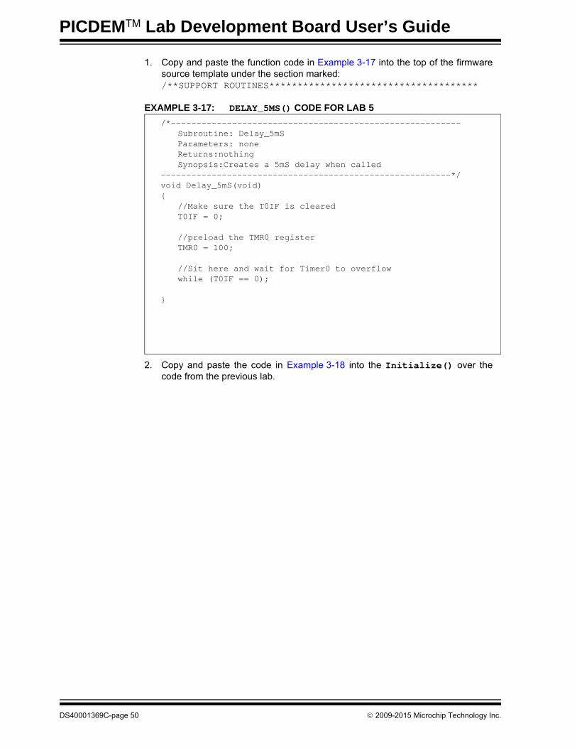
PICDEMTM Lab Development Board User’s Guide
1. Copy and paste the function code in Example 3-17 into the top of the firmwaresource template under the section marked:/**SUPPORT ROUTINES*************************************
EXAMPLE 3-17: DELAY_5MS() CODE FOR LAB 5
2. Copy and paste the code in Example 3-18 into the Initialize() over thecode from the previous lab.
/*---------------------------------------------------------Subroutine: Delay_5mSParameters: noneReturns:nothingSynopsis:Creates a 5mS delay when called
---------------------------------------------------------*/void Delay_5mS(void)
//Make sure the T0IF is clearedT0IF = 0;
//preload the TMR0 registerTMR0 = 100;
//Sit here and wait for Timer0 to overflowwhile (T0IF == 0);
DS40001369C-page 50 2009-2015 Microchip Technology Inc.

General Purpose Input/Output Labs
EXAMPLE 3-18: INITIALIZE() FOR GPIO LAB 5
//Clear PORTC to a known state//Set the least significant bit to 1 so that it can be//shifted throughPORTC = 0b00000001;
//Clear the PORTA register to a known statePORTA = 0b00000000;
//Configure PORTC's ANALOG/DIGITAL pins as all DigitalANS4 = 0;//Associated with RC0ANS5 = 0;//Associated with RC1ANS6 = 0;//Associated with RC2ANS7 = 0;//Associated with RC3ANS8 = 0;//Associated with RC6ANS9 = 0;//Associated with RC7
//Configure PORTC pins as all output//i.e. 1 = Input, 0 = OutputTRISC0 = 0;//Associated with RC0TRISC1 = 0;//Associated with RC1TRISC2 = 0;//Associated with RC2TRISC3 = 0;//Associated with RC3TRISC4 = 0;//Associated with RC4TRISC5 = 0;//Associated with RC5TRISC6 = 0;//Associated with RC6TRISC7 = 0;//Associated with RC7
//Configure PORTA bit RA0 as Digital inputANS2 = 0;TRISA2 = 1;
//Configure Timer0 to overflow every 5mST0CS = 0; //Select FOSC/4 as Timer0 clock sourceT0SE = 0; //Increment TMR0 on rising clock edgePSA = 0; //Assign prescaler to Timer0//Select a 1:32 prescaler PS0 = 0;PS1 = 0;PS2 = 1;
//Initialize the direction flag to shift bits from //right-to-left//(i.e. 0 = Shift PORTC bits from right-to-left// 1 = Shift PORTC bits from left-to-rightdirection = 0;
//Initialize LED_Output to all zerosLED_Output = 0b00000000;
2009-2015 Microchip Technology Inc. DS40001369C-page 51

PICDEMTM Lab Development Board User’s Guide
3. Copy and paste the code in Example 3-19 into the Get_Inputs() at the sectionlabeled://ADD GET_INPUTS CODE HERE
EXAMPLE 3-19: GET_INPUTS() CODE FOR GPIO LAB 5
4. Copy and paste the code in Example 3-20 into the Decide() over the code fromthe previous lab.
EXAMPLE 3-20: DECIDE() CODE FOR GPIO LAB 5
//Check for a push button press (i.e. RA2 = 0)if (RA2 == 0)
Delay_5mS(); //Delay to debounce
//Check if push button is still pressedif(RA2 == 0) direction ^= 1; //If so, toggle the
//direction bit//Otherwise keep direction the same as it waselse direction = direction;
if(direction == 0)//First check if LED_Output variable has most //significant bit set to 1 or if LED_Output variable is //all 0's.//If so, re initialize the LED_Output variable so that //the most significant bit is set to 1 and all other //bits are 0
if((LED_Output == 0b00000001) || (LED_Output == 0b00000000)) LED_Output = 0b10000000;
//If neither of these conditions are true, simply shift//the LED_Output variable's contents to the Left by 1 //bit position
else LED_Output >>=1;
else//First check if LED_Output variable has the least //significant bit set//to 1 or if LED_Output variable is all 0's.//If so, re initialize the LED_Output variable so that //the least significant bit is set to 1 and all other //bits are 0
if((LED_Output == 0b10000000) || (LED_Output == 0b00000000)) LED_Output = 0b00000001;
//If neither of these conditions are true, simply shift//the LED_Output variable's contents to the Right by 1 //bit position
else LED_Output <<=1;
DS40001369C-page 52 2009-2015 Microchip Technology Inc.
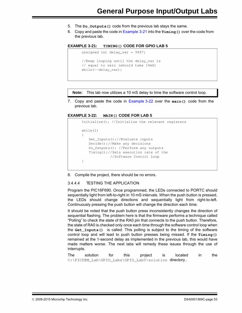
General Purpose Input/Output Labs
5. The Do_Outputs() code from the previous lab stays the same.
6. Copy and paste the code in Example 3-21 into the Timing() over the code fromthe previous lab.
EXAMPLE 3-21: TIMING() CODE FOR GPIO LAB 5
7. Copy and paste the code in Example 3-22 over the main() code from theprevious lab.
EXAMPLE 3-22: MAIN() CODE FOR LAB 5
8. Compile the project, there should be no errors.
3.4.4.4 TESTING THE APPLICATION
Program the PIC16F690. Once programmed, the LEDs connected to PORTC shouldsequentially light from left-to-right in 10 mS intervals. When the push button is pressed,the LEDs should change directions and sequentially light from right-to-left.Continuously pressing the push button will change the direction each time.
It should be noted that the push button press inconsistently changes the direction ofsequential flashing. The problem here is that the firmware performs a technique called“Polling” to check the state of the RA0 pin that connects to the push button. Therefore,the state of RA0 is checked only once each time through the software control loop whenthe Get_Inputs() is called. This polling is subject to the timing of the softwarecontrol loop and will lead to push button presses being missed. If the Timing()remained at the 1-second delay as implemented in the previous lab, this would havemade matters worse. The next labs will remedy these issues through the use ofinterrupts.
The solution for this project is located in theC:\PICDEM_Lab\GPIO_Labs\GPIO_Lab5\solution directory.
unsigned int delay_var = 9997;
//Keep looping until the delay_var is // equal to zero (should take 10mS)while(--delay_var);
Note: This lab now utilizes a 10 mS delay to time the software control loop.
Initialize(); //Initialize the relevant registers
while(1)
Get_Inputs();//Evaluate inputsDecide();//Make any decisions Do_Outputs(); //Perform any outputsTiming();//Sets execution rate of the
//Software Control Loop
2009-2015 Microchip Technology Inc. DS40001369C-page 53

PICDEMTM Lab Development Board User’s Guide
3.4.5 Lab 6: Push Button Interrupt
3.4.5.1 NEW REGISTERS USED IN THIS LAB
To configure the peripherals used in this lab, the following registers are used:
1. OPTION Register: OPTION (Register 2-2 in Section 2 of the PIC16F690 DataSheet)
- Selects the edge transition on RA2/INT that will trigger an interrupt.
2. Interrupt Control Register: INTCON (Register 2-3 in Section 2 of the PIC16F690Data Sheet)
- Enable interrupt functionality on the PIC16F690.
- Enables the RA2/INT external interrupt.
- Contains a flag that indicates the external interrupt has occurred.
3.4.5.2 OVERVIEW
This lab expands upon Lab 5 by adding an interrupt that will occur each time the pushbutton connected to the RA2 pin is pressed.
As mentioned, polling a bit is heavily reliant on a number of factors such as the size ofthe firmware and the timing of the software control loop. Polling does have its uses.However, there may be times when an event, such as pressing a push button, requiresimmediate attention. This is where the interrupt comes in. As the name implies, aninterrupt acts as a sort of alarm. When the Central Processing Unit receives aninterrupt, it immediately stops what it is doing, saves where in the code it was beforethe interrupt, performs code or firmware defined by the user in the event of an interruptcalled an Interrupt Service Routine (ISR), and then returns to the previous task it wasperforming prior to the interrupt.
So, why not use interrupts all the time? The answer is mainly cost. In order toimplement an interrupt for a specific function, the user may need to purchase amicrocontroller with a peripheral that accommodates the interrupt. This increases thecost of the application. In some cases, polling a bit may be the way to go. Other casesmay require the interrupt thereby justifying the added cost of a particular peripheral.
The RA2 pin associated with the PORTA register features an external edge-triggeredinterrupt capability (note the INT designation on the PIC16F690 Pin Diagram in Table5 of the data sheet). The interrupt is configurable to occur on either the rising-edge (i.e.,signal on RA2 pin transitions from low-to-high) or the falling-edge (i.e., signal on RA2pin transitions from high-to-low) of the voltage on the RA2 pin. If the selected edgetransition is detected on RA2, the CPU then services the interrupt before returning tothe code it was executing prior to the interrupt. Referring again to Figure 3-12, the pushbutton connected to the RA2 pin is pulled high when not pressed. Therefore, theinterrupt will be configured to trigger on the high-to-low transition indicating a pushbutton press.
The INTCON register contains the enable (INTE) and flag (INTF) bits for the RA2external interrupt. These bits indicate to firmware the condition that caused an interruptto occur. The other bits and accompanying registers are used for other peripheralfeatures on the microcontroller. The Global Interrupt Enable bit (GIE) is a sort of masterswitch that allows interrupts, if individually enabled, to be used by the microcontroller.
The OPTION register features the Interrupt Edge Select (INTEDG) bit that will be usedto indicate the edge transition that will trigger an interrupt.
The software flowchart for this lab is shown in Figure 3-26.
DS40001369C-page 54 2009-2015 Microchip Technology Inc.

General Purpose Input/Output Labs
FIGURE 3-26: MAIN() SOFTWARE CONTROL LOOP FLOWCHART FOR GPIO LAB 6
Note the removal of the Get_Inputs() from the previous lab. This code will now behandled by an Interrupt Service Routine (ISR) whenever the push button is pressed.The PB_PressISR() flowchart is shown in Figure 3-27.
FIGURE 3-27: PB_PRESSISR() FOR LAB 6 SHOWING SWITCH DEBOUNCE
main()
Initialize()
Do_Outputs() Loop Forever
Timing()
Decide()
Global Variables:
• 8-bit variable LED_Output will be used to light the LEDs connected to PORTC
• 1-bit variable direction used to determine the direction of the sequential LED flashing0 = shift PORTC bits right-to-left1 = shift PORTC bits left-to-right
PB_PressISR()
INTE and INTF
bits set
?
RETURN
NO
Clear INTF flag
YES
RA2 pin = 0
?
direction = direction
Delay for 5mSYES
RA2 pin = 0
?
Toggle direction
YES
NO
NO
2009-2015 Microchip Technology Inc. DS40001369C-page 55
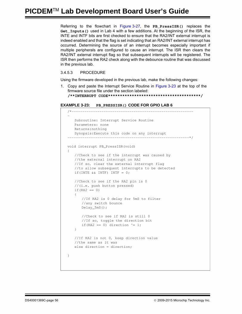
PICDEMTM Lab Development Board User’s Guide
Referring to the flowchart in Figure 3-27, the PB_PressISR() replaces theGet_Inputs() used in Lab 4 with a few additions. At the beginning of the ISR, theINTE and INTF bits are first checked to ensure that the RA2/INT external interrupt isindeed enabled and that the flag is set indicating that an RA2/INT external interrupt hasoccurred. Determining the source of an interrupt becomes especially important ifmultiple peripherals are configured to cause an interrupt. The ISR then clears theRA2/INT external interrupt flag so that subsequent interrupts will be registered. TheISR then performs the RA2 check along with the debounce routine that was discussedin the previous lab.
3.4.5.3 PROCEDURE
Using the firmware developed in the previous lab, make the following changes:
1. Copy and paste the Interrupt Service Routine in Figure 3-23 at the top of thefirmware source file under the section labeled:/**INTERRUPT CODE***************************************/
EXAMPLE 3-23: PB_PRESSISR() CODE FOR GPIO LAB 6
/*----------------------------------------------------------
Subroutine: Interrupt Service RoutineParameters: noneReturns:nothingSynopsis:Execute this code on any interrupt
---------------------------------------------------------*/
void interrupt PB_PressISR(void)
//Check to see if the interrupt was caused by //the external interrupt on RA2//If so, clear the external interrupt flag//to allow subsequent interrupts to be detectedif(INTE && INTF) INTF = 0;
//Check to see if the RA2 pin is 0//(i.e. push button pressed)if(RA2 == 0)
//If RA2 is 0 delay for 5mS to filter//any switch bounceDelay_5mS();
//Check to see if RA2 is still 0//If so, toggle the direction bitif(RA2 == 0) direction ^= 1;
//If RA2 is not 0, keep direction value//the same as it waselse direction = direction;
DS40001369C-page 56 2009-2015 Microchip Technology Inc.

General Purpose Input/Output Labs
2. Copy and paste the code in Example 3-24 into the Initialize() over thecode from the previous lab.
Note: To indicate a function that should be used whenever an interrupt occurs, the interrupt function qualifier is needed. This qualifier is specific to the HI-TECH C Compiler.
2009-2015 Microchip Technology Inc. DS40001369C-page 57
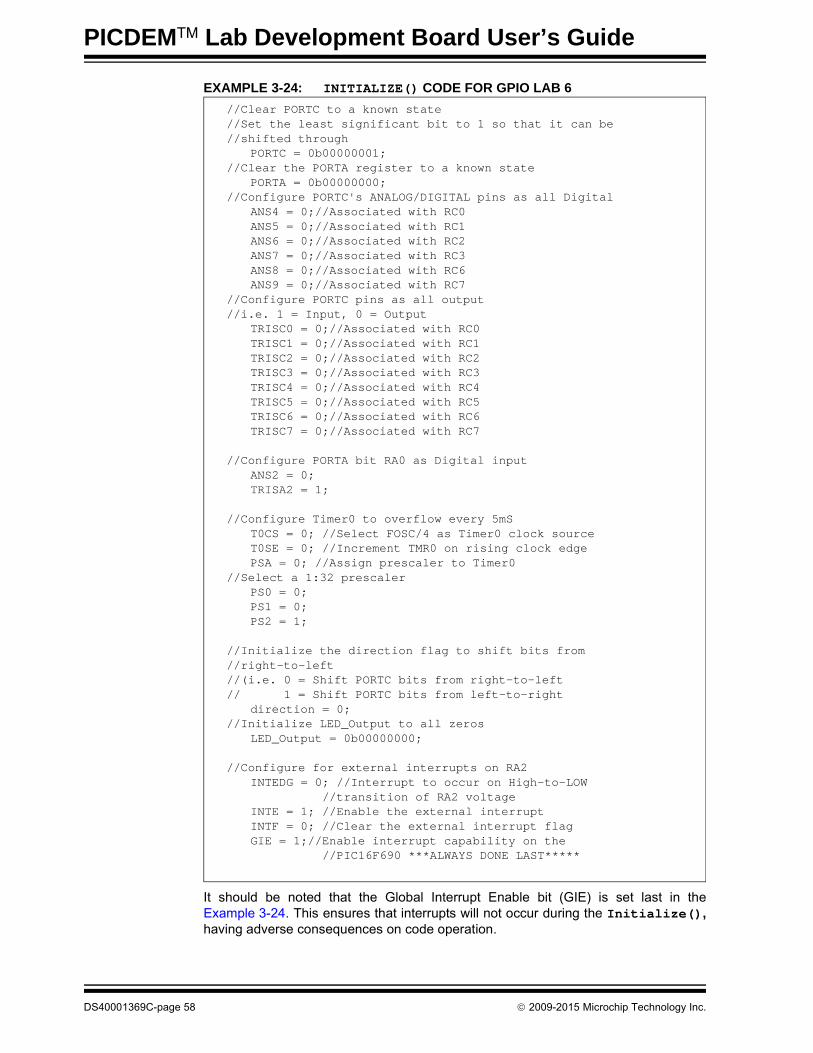
PICDEMTM Lab Development Board User’s Guide
EXAMPLE 3-24: INITIALIZE() CODE FOR GPIO LAB 6
It should be noted that the Global Interrupt Enable bit (GIE) is set last in theExample 3-24. This ensures that interrupts will not occur during the Initialize(),having adverse consequences on code operation.
//Clear PORTC to a known state//Set the least significant bit to 1 so that it can be//shifted through
PORTC = 0b00000001;//Clear the PORTA register to a known state
PORTA = 0b00000000;//Configure PORTC's ANALOG/DIGITAL pins as all Digital
ANS4 = 0;//Associated with RC0ANS5 = 0;//Associated with RC1ANS6 = 0;//Associated with RC2ANS7 = 0;//Associated with RC3ANS8 = 0;//Associated with RC6ANS9 = 0;//Associated with RC7
//Configure PORTC pins as all output//i.e. 1 = Input, 0 = Output
TRISC0 = 0;//Associated with RC0TRISC1 = 0;//Associated with RC1TRISC2 = 0;//Associated with RC2TRISC3 = 0;//Associated with RC3TRISC4 = 0;//Associated with RC4TRISC5 = 0;//Associated with RC5TRISC6 = 0;//Associated with RC6TRISC7 = 0;//Associated with RC7
//Configure PORTA bit RA0 as Digital inputANS2 = 0;TRISA2 = 1;
//Configure Timer0 to overflow every 5mST0CS = 0; //Select FOSC/4 as Timer0 clock sourceT0SE = 0; //Increment TMR0 on rising clock edgePSA = 0; //Assign prescaler to Timer0
//Select a 1:32 prescaler PS0 = 0;PS1 = 0;PS2 = 1;
//Initialize the direction flag to shift bits from //right-to-left//(i.e. 0 = Shift PORTC bits from right-to-left// 1 = Shift PORTC bits from left-to-right
direction = 0;//Initialize LED_Output to all zeros
LED_Output = 0b00000000;
//Configure for external interrupts on RA2INTEDG = 0; //Interrupt to occur on High-to-LOW
//transition of RA2 voltageINTE = 1; //Enable the external interrupt INTF = 0; //Clear the external interrupt flagGIE = 1;//Enable interrupt capability on the
//PIC16F690 ***ALWAYS DONE LAST*****
DS40001369C-page 58 2009-2015 Microchip Technology Inc.

General Purpose Input/Output Labs
3. Copy and paste the code in Example 3-25 into the main() over the code fromthe previous lab to remove the Get_Inputs().
EXAMPLE 3-25: MAIN() CODE FOR GPIO LAB 6
4. The remaining code remains unchanged from the previous lab. Compile theproject. There should be no errors.
3.4.5.4 TESTING THE APPLICATION
Program the PIC16F690. The application should behave as it did in the previous lab. Only this time, the change in LED flashing direction should now be more responsive to push button presses due to the interrupt added.
The solution for this project is located in the C:\PICDEM_Lab\GPIO_Labs\GPIO_Lab6\solution directory.
3.4.6 Lab 7: Push Button Interrupt-on-Change
3.4.6.1 NEW REGISTERS USED IN THIS LAB
To configure the peripherals used in this lab, the following registers are used:
1. Interrupt-on-Change PORTA Register: IOCA (Register 4-6 in Section 4 of thePIC16F690 Data Sheet).
- Configures PORTA associated pins that will generate an interrupt when achange in voltage level is detected.
2. Interrupt Control Register: INTCON (Register 2-3 in Section 2 of the PIC16F690Data Sheet)
- Enable interrupt functionality on the PIC16F690.
- Enables PORTA/PORTB change interrupts.
- Contains a flag that indicates that a PORTA or PORTB change interrupt hasoccurred.
3.4.6.2 OVERVIEW
This lab adds a different kind of interrupt associated with the General PurposeInput/Output peripheral called interrupt-on-change. Rather than simply interrupting theCPU on a single edge transition on the RA2 pin, an interrupt will now occur on any edgetransition. Therefore, when the push button is pressed and/or released, an interrupt willoccur. This lab will use these concepts to shift the flashing LEDs from left-to-right whilethe push button is pressed and from right-to-left when the push button is released.
Each PORTA and PORTB pin is individually configurable as an interrupt-on-changepin. Control bits in the Interrupt-on-Change PORTA register (IOCA) enable or disablethe interrupt function for each pin.
Initialize(); //Initialize the relevant registers
while(1)
Decide();//Make any decisions Do_Outputs(); //Perform any outputsTiming();//Sets execution rate of the
//Software Control Loop
2009-2015 Microchip Technology Inc. DS40001369C-page 59
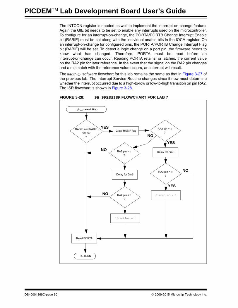
PICDEMTM Lab Development Board User’s Guide
The INTCON register is needed as well to implement the interrupt-on-change feature.Again the GIE bit needs to be set to enable any interrupts used on the microcontroller.To configure for an interrupt-on-change, the PORTA/PORTB Change Interrupt Enablebit (RABIE) must be set along with the individual enable bits in the IOCA register. Onan interrupt-on-change for configured pins, the PORTA/PORTB Change Interrupt Flagbit (RABIF) will be set. To detect a logic change on a port pin, the firmware needs toknow what has changed. Therefore, PORTA must be read before aninterrupt-on-change can occur. Reading PORTA retains, or latches, the current valueon the RA2 pin for later reference. In the event that the signal on the RA2 pin changesand a mismatch with the reference value occurs, an interrupt will result.
The main() software flowchart for this lab remains the same as that in Figure 3-27 ofthe previous lab. The Interrupt Service Routine changes since it now must determinewhether the interrupt occurred due to a high-to-low or low-to-high transition on pin RA2.The ISR flowchart is shown in Figure 3-28.
FIGURE 3-28: PB_PRESSISR FLOWCHART FOR LAB 7
pb_pressISR()
RABIE and RABIF
bits set
?
RETURN
Clear RABIF flagYES RA2 pin = 0
?
direction = 1
Delay for 5mS
NORA2 pin = 0
?
RA2 pin = 1
?
Delay for 5mS
RA2 pin = 1
?
direction = 1
Read PORTA
YES
YES
NO
NO
NO
DS40001369C-page 60 2009-2015 Microchip Technology Inc.

General Purpose Input/Output Labs
The PB_PressISR() now checks to see if the voltage level on RA2 has changedstate from a 1-to-0 or from 0-to-1. Each condition will change the direction that theLEDs flash sequentially. Note that the direction bit toggle used in previous labs hasbeen replaced by assigning either a ‘1’ for the left-to-right direction or ‘0’ for theright-to-left direction. As discussed earlier, the PORTA register must be read before thefirst interrupt can occur and at the end of each subsequent ISR execution to ensure thatthe microcontroller has an up-to-date reference to measure the current state of the RA2pin.
The Initialize() for this lab configures the peripherals and interrupts as follows:
• PORTC
- Clears PORTC
- Configures all pins as digital output
• PORTA
- Clears PORTA
- Configures RA2 as a digital input
• Timer0
- Uses the FOSC/4 as clock source
- Increment TMR0 on rising FOSC/4 clock edge
- Use Prescaler at 1:32
• Global Variables
- Initialize direction to ‘0’
- Initialize LED_Output to ‘0’
• Interrupt
- Enable RA2 Interrupt-on-Change
- Enable change interrupts in INTCON by setting the RABIE bit
- Clear the RABIF change interrupt flag in INTCON
- Enable Global Interrupts by setting GIE
- Read PORTA to latch current value on RA2 for reference
3.4.6.3 PROCEDURE
Using the firmware developed in the previous lab, make the following changes:
1. Copy and paste the code in Example 3-26 into the PB_PressISR() over thecode from the previous lab.
2009-2015 Microchip Technology Inc. DS40001369C-page 61

PICDEMTM Lab Development Board User’s Guide
EXAMPLE 3-26: PB_PRESSISR() CODE FOR GPIO LAB 7
2. Copy and paste the code in Example 3-27 into the Initialize() over thecode from the previous lab.
//First, check if the interrupt occurred as a result of an //RA2 change interrupt. If so, clear the RABIF flag so //that subsequent interrupts can occurif(RABIE && RABIF) RABIF = 0;//Check the push button connected to RA0 pin. If 0, then a //push button press is indicated
if(RA2 == 0)
//Delay for 5mS to filter switch bounceDelay_5mS();
//if RA2 is still 0 then change the direction flagif (RA2 == 0) direction = 1;
//Check the push button connected to RA0 pin. If 1, then a //push button release is indicated
if(RA2 == 1)
//Delay for 5mS to filter switch bounceDelay_5mS();
//if RA2 is still 1 then change the direction flagif (RA2 == 1) direction = 0;
//Otherwise, keep the direction bit the same as it was
else direction = direction;
//Read PORTA to latch RA2 value for the next interruptPORTA = PORTA;
DS40001369C-page 62 2009-2015 Microchip Technology Inc.

General Purpose Input/Output Labs
EXAMPLE 3-27: INITIALIZE() CODE FOR GPIO LAB 7
//Clear PORTC to a known state//Set the least significant bit to 1 so that it can be//shifted through
PORTC = 0b00000001;
//Clear the PORTA register to a known statePORTA = 0b00000000;
//Configure PORTC's ANALOG/DIGITAL pins as all DigitalANS4 = 0;//Associated with RC0ANS5 = 0;//Associated with RC1ANS6 = 0;//Associated with RC2ANS7 = 0;//Associated with RC3ANS8 = 0;//Associated with RC6ANS9 = 0;//Associated with RC7
//Configure PORTC pins as all output//i.e. 1 = Input, 0 = Output
TRISC0 = 0;//Associated with RC0TRISC1 = 0;//Associated with RC1TRISC2 = 0;//Associated with RC2TRISC3 = 0;//Associated with RC3TRISC4 = 0;//Associated with RC4TRISC5 = 0;//Associated with RC5TRISC6 = 0;//Associated with RC6TRISC7 = 0;//Associated with RC7
//Configure PORTA bit RA0 as Digital inputANS2 = 0;TRISA2 = 1;
//Configure Timer0 to overflow every 5mST0CS = 0; //Select FOSC/4 as Timer0 clock sourceT0SE = 0; //Increment TMR0 on rising clock edgePSA = 0; //Assign prescaler to Timer0
//Select a 1:32 prescaler PS0 = 0;PS1 = 0;PS2 = 1;
//Initialize the direction flag to shift bits from right-to-left//(i.e. 0 = Shift PORTC bits from right-to-left// 1 = Shift PORTC bits from left-to-right
direction = 0;
//Initialize LED_Output to all zerosLED_Output = 0b00000000;
//Configure for RA2 Interrupt-On-ChangeIOCA2 = 1; //Enable RA2 interrupt-on-changeRABIE = 1; //Enable change interruptsRABIF = 0; //Clear the change interrupt flagGIE = 1;//Enable interrupt capability on the
//PIC16F690 ***ALWAYS DONE LAST*****
//Read PORTA to latch the current RA2 voltage levelPORTA = PORTA;
2009-2015 Microchip Technology Inc. DS40001369C-page 63

PICDEMTM Lab Development Board User’s Guide
3. All remaining code from the previous lab is unchanged. Compile the project.There should be no errors.
3.4.6.4 TESTING THE APPLICATION
Program the PIC16F690. The LEDs connected to PORTC should now flashsequentially from left-to-right when the push button is released and flash fromright-to-left when the push button is pressed.
The solution for this project is located in the C:\PICDEM_Lab\GPIO_Labs\GPIO_Lab7\solution directory.
3.4.7 Lab 8: Using Weak Pull-Ups
3.4.7.1 NEW REGISTERS USED IN THIS LAB
To configure the peripherals used in this lab, the following registers are used:
1. OPTION Register: OPTION (Register 2-2 in Section 2 of the PIC16F690 DataSheet)
- Enables PORTA/PORTB weak pull-ups to be used on the PIC16F690.
2. PORTA Weak Pull-Up Register: WPUA (Register 4-5 in Section 4 of thePIC16F690 Data Sheet)
- Selects which PORTA pins will have weak pull-ups enabled.
3.4.7.2 OVERVIEW
This lab expands on the previous lab by adding weak pull-ups to remove the 10 kused previously to tie RA2 pin to VDD. Each of the PORTA pins (except RA3) andPORTB pins, has an individually configurable internal weak pull-up. Essentially, theseweak pull-ups perform the same task as the resistor connected to the RA2 pin and pushbutton as shown in Figure 3-12 only internal to the microcontroller. This feature can beused to decrease component counts in the circuit.
Clearing the PORTA/PORTB Pull-up Enable bit, RABPU, in the OPTION register willenable weak pull-ups on any PORTA pin selected using the Weak Pull-Up PORTAregister (WPUA).
The only change needed to the PICDEM Lab Development Board Schematic shown inFigure 3-21 is to remove the 10 kresistor connected to both the push button and pinRA2.
The Initialize() is all that needs to be changed in firmware by adding the followingconfigurations:
• Select RA2 to have a weak pull-up by setting the Weak Pull-Up Register bitWPUA2 in the WPUA: PORTA Register.
• Enable the PORTA/PORTB Pull-up Enable bit (RABPU) in the OPTION registerby clearing it.
3.4.7.3 PROCEDURE
Using the firmware developed in the previous lab, make the following changes:
1. Copy/paste the code in Example 3-28 into the Initialize() over the codefrom the previous lab.
DS40001369C-page 64 2009-2015 Microchip Technology Inc.
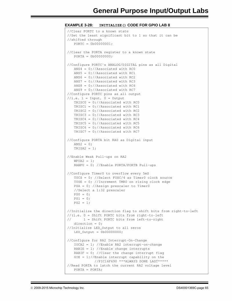
General Purpose Input/Output Labs
EXAMPLE 3-28: INITIALIZE() CODE FOR GPIO LAB 8
//Clear PORTC to a known state//Set the least significant bit to 1 so that it can be//shifted through
PORTC = 0b00000001;
//Clear the PORTA register to a known statePORTA = 0b00000000;
//Configure PORTC's ANALOG/DIGITAL pins as all DigitalANS4 = 0;//Associated with RC0ANS5 = 0;//Associated with RC1ANS6 = 0;//Associated with RC2ANS7 = 0;//Associated with RC3ANS8 = 0;//Associated with RC6ANS9 = 0;//Associated with RC7
//Configure PORTC pins as all output//i.e. 1 = Input, 0 = Output
TRISC0 = 0;//Associated with RC0TRISC1 = 0;//Associated with RC1TRISC2 = 0;//Associated with RC2TRISC3 = 0;//Associated with RC3TRISC4 = 0;//Associated with RC4TRISC5 = 0;//Associated with RC5TRISC6 = 0;//Associated with RC6TRISC7 = 0;//Associated with RC7
//Configure PORTA bit RA0 as Digital inputANS2 = 0;TRISA2 = 1;
//Enable Weak Pull-ups on RA2WPUA2 = 1;RABPU = 0; //Enable PORTA/PORTB Pull-ups
//Configure Timer0 to overflow every 5mST0CS = 0; //Select FOSC/4 as Timer0 clock sourceT0SE = 0; //Increment TMR0 on rising clock edgePSA = 0; //Assign prescaler to Timer0//Select a 1:32 prescaler PS0 = 0;PS1 = 0;PS2 = 1;
//Initialize the direction flag to shift bits from right-to-left//(i.e. 0 = Shift PORTC bits from right-to-left// 1 = Shift PORTC bits from left-to-right
direction = 0;//Initialize LED_Output to all zeros
LED_Output = 0b00000000;
//Configure for RA2 Interrupt-On-ChangeIOCA2 = 1; //Enable RA2 interrupt-on-changeRABIE = 1; //Enable change interruptsRABIF = 0; //Clear the change interrupt flagGIE = 1;//Enable interrupt capability on the
//PIC16F690 ***ALWAYS DONE LAST*****//Read PORTA to latch the current RA2 voltage level
PORTA = PORTA;
2009-2015 Microchip Technology Inc. DS40001369C-page 65
PICDEMTM Lab Development Board User’s Guide
3.4.7.4 TESTING THE APPLICATION
Program the PIC16F690. The application should operate exactly as it did in theprevious lab. Only this time with the absence of the 10 kpull-up resistor.
The solution for this project is located in the C:\PICDEM_Lab\GPIO_Labs\GPIO_Lab8\solution directory.
DS40001369C-page 66 2009-2015 Microchip Technology Inc.
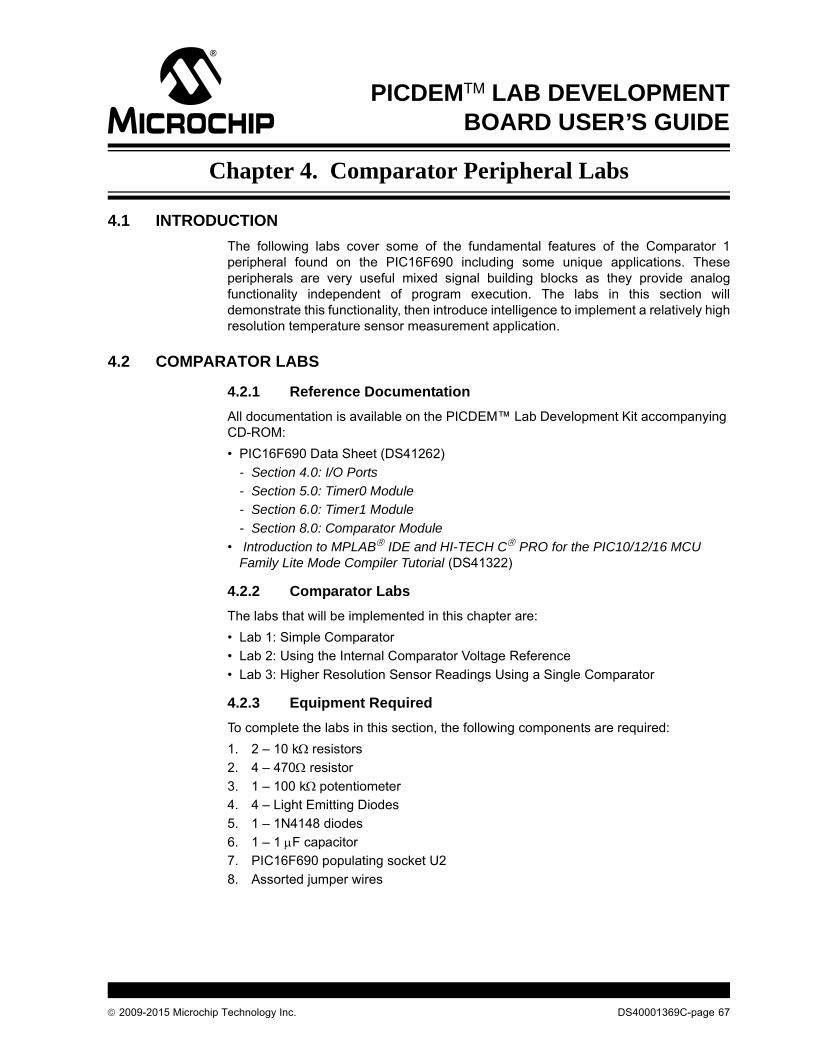
PICDEMTM LAB DEVELOPMENT
BOARD USER’S GUIDEChapter 4. Comparator Peripheral Labs
4.1 INTRODUCTION
The following labs cover some of the fundamental features of the Comparator 1peripheral found on the PIC16F690 including some unique applications. Theseperipherals are very useful mixed signal building blocks as they provide analogfunctionality independent of program execution. The labs in this section willdemonstrate this functionality, then introduce intelligence to implement a relatively highresolution temperature sensor measurement application.
4.2 COMPARATOR LABS
4.2.1 Reference Documentation
All documentation is available on the PICDEM™ Lab Development Kit accompanying CD-ROM:
• PIC16F690 Data Sheet (DS41262)
- Section 4.0: I/O Ports
- Section 5.0: Timer0 Module
- Section 6.0: Timer1 Module
- Section 8.0: Comparator Module
• Introduction to MPLAB IDE and HI-TECH C PRO for the PIC10/12/16 MCU Family Lite Mode Compiler Tutorial (DS41322)
4.2.2 Comparator Labs
The labs that will be implemented in this chapter are:
• Lab 1: Simple Comparator
• Lab 2: Using the Internal Comparator Voltage Reference
• Lab 3: Higher Resolution Sensor Readings Using a Single Comparator
4.2.3 Equipment Required
To complete the labs in this section, the following components are required:
1. 2 – 10 kresistors
2. 4 – 470 resistor
3. 1 – 100 kpotentiometer
4. 4 – Light Emitting Diodes
5. 1 – 1N4148 diodes
6. 1 – 1 F capacitor
7. PIC16F690 populating socket U2
8. Assorted jumper wires
2009-2015 Microchip Technology Inc. DS40001369C-page 67
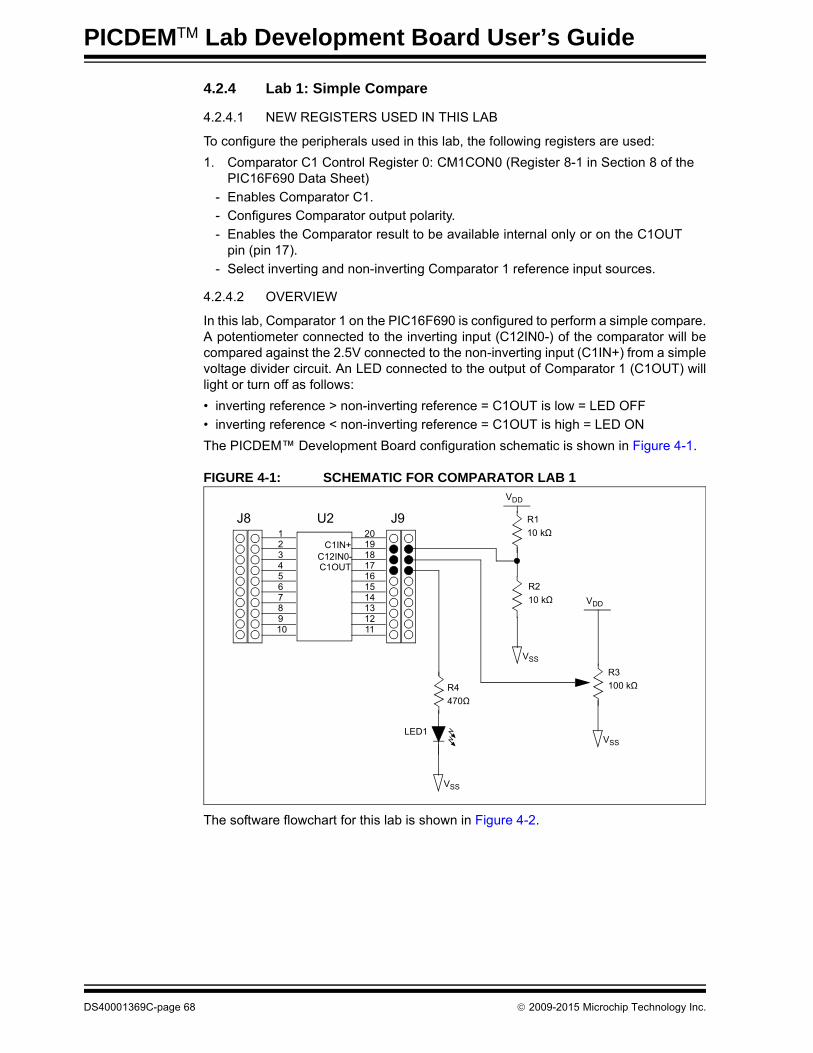
PICDEMTM Lab Development Board User’s Guide
4.2.4 Lab 1: Simple Compare
4.2.4.1 NEW REGISTERS USED IN THIS LAB
To configure the peripherals used in this lab, the following registers are used:
1. Comparator C1 Control Register 0: CM1CON0 (Register 8-1 in Section 8 of thePIC16F690 Data Sheet)
- Enables Comparator C1.
- Configures Comparator output polarity.
- Enables the Comparator result to be available internal only or on the C1OUTpin (pin 17).
- Select inverting and non-inverting Comparator 1 reference input sources.
4.2.4.2 OVERVIEW
In this lab, Comparator 1 on the PIC16F690 is configured to perform a simple compare.A potentiometer connected to the inverting input (C12IN0-) of the comparator will becompared against the 2.5V connected to the non-inverting input (C1IN+) from a simplevoltage divider circuit. An LED connected to the output of Comparator 1 (C1OUT) willlight or turn off as follows:
• inverting reference > non-inverting reference = C1OUT is low = LED OFF
• inverting reference < non-inverting reference = C1OUT is high = LED ON
The PICDEM™ Development Board configuration schematic is shown in Figure 4-1.
FIGURE 4-1: SCHEMATIC FOR COMPARATOR LAB 1
The software flowchart for this lab is shown in Figure 4-2.
U212345678910
20191817161514131211
C1IN+
J9J8
R4
470Ω
LED1
VSS
VDD
C12IN0-C1OUT
R1
10 kΩ
R2
10 kΩ VDD
R3
100 kΩ
VSS
VSS
DS40001369C-page 68 2009-2015 Microchip Technology Inc.

Comparator Peripheral Labs
FIGURE 4-2: MAIN() SOFTWARE CONTROL LOOP FLOWCHART FOR COMPARATOR LAB 1
As mentioned in the introduction, comparators on the PIC16F690 are able to functionindependent of software logic. Therefore, all that is needed is to call theInitialize() from main() to activate the peripheral. The Initialize()configures Comparator 1 as follows:
• Turn on Comparator 1
• Make the Comparator 1 output available on the C1OUT pin
• Select pin C1IN+ as the non-inverting reference
• Select pin C12IN0- as the inverting reference
• Configure the C1OUT pin as an output
4.2.4.3 PROCEDURE
Using the Project Wizard, create a new project using the PIC16F690 entitledComparator_Lab1.mcp as was done in previous labs. Once completed, open theComparator_Lab2.c source file in MPLAB and do the following:
1. Copy/paste the code in Example 4-1 into the Initialize() section labeled://ADD INITIALIZE CODE HERE
EXAMPLE 4-1: INITIALIZE CODE FOR COMPARATOR LAB 1
main()
Initialize()
Loop ForeverWait
//Initialize Comparator 1 as follows:
//Turn comparator 1 onC1ON = 1;
//Make the comparator output available on the //C1OUT pinC1OE = 1;
//Select the non-inverting pin (C1IN+) as the //non-inverting reference input for the comparator 1C1R = 0;
//Select the C12IN0- pin as the inverting referenceC1CH0 = 0;C1CH1 = 0;
//Since the comparator 1 output shares the same pin//as PORTA bit 2, configure the corresponding TRISA2 bit//as an outputTRISA2 = 0;
2009-2015 Microchip Technology Inc. DS40001369C-page 69

PICDEMTM Lab Development Board User’s Guide
2. Copy and paste the code in Example 4-2 into the main() section labeled://ADD MAIN CODE HERE
EXAMPLE 4-2: MAIN() CODE FOR COMPARATOR LAB 1
3. Compile the project. There should be no errors.
4.2.4.4 TESTING THE APPLICATION
Program the PIC16F690. The LED connected to the C1OUT pin should light when thevoltage present on the C12IN0- pin is less than the 2.5V present on the C1IN+ pin andturn off when the 2.5V is exceeded.
The solution for this project is located in the C:\PICDEM_Lab\Comparator_Labs\Comparator_Lab1\solution directory.
4.2.5 Lab 2: Using the Comparator Voltage Reference
4.2.5.1 NEW REGISTERS USED IN THIS LAB
To configure the peripherals used in this lab, the following registers are used:
1. Voltage Reference Control Register: VRCON (Register 8-5 in Section 8 of thePIC16F690 Data Sheet).
- Enables either the Comparator Voltage Reference or the 0.6V constantreference as the non-inverting reference input to Comparator C1 orComparator C2.
- Selects either a High or Low resolution 16-level voltage range.
- Enable a 0.6V reference.
- Uses three bits to configure the reference voltage level.
4.2.5.2 OVERVIEW
This lab expands on Lab 1 by utilizing the internal Comparator Voltage Reference(CVREF) feature on the PIC16F690. The CVREF provides an internally generatedvoltage reference that can be used by the Comparator 1 non-inverting reference inputso that external components are not needed such as the resistor voltage divider usedin the previous lab. The CVREF features:
• Independent comparator operation
• Two 16-level voltage ranges
• Ratiometric with VDD
• Fixed 0.6 reference option
• Output clamped to VSS
Initialize(); //Initialize the relevant registerswhile(1);
Note: The inclusion of the while loop forces the microcontroller to sit and wait at a “known” instruction. At start-up, the contents of the program memory are unknown. Without the while loop, the microcontroller will continue to run through each address in program memory executing whatever resides at a particular address. This could have adverse effects on the application.
Note: This application uses two pins that are used during the programming pro-cess (ICSPDATA and ICSPCLK). The jumper wires connecting these pins to the application circuit may need to be disconnected while programming if there are problems with the MPLAB IDE connecting to the PIC16F690.
DS40001369C-page 70 2009-2015 Microchip Technology Inc.

Comparator Peripheral Labs
The CVREF has two ranges with 16 voltage levels in each range. Range selection iscontrolled by the CVREF Range Selection (VRR) bit in the VRCON (Voltage ReferenceControl Register) along with the CVREF Value Selection bits (VR<3:0>). The ValueSelection bits hold a value based upon some simple calculations to set the internalreference voltage. The CVREF voltage is determined using Equation 4-1:
EQUATION 4-1: CVREF OUTPUT VOLTAGE
This lab will implement the low-range calculation by setting the VRR bit in VRCONequal to 1. Equation 4-2 demonstrates how to calculate the VR<3:0> values, using thelow-range method, to obtain a 2.5V internal reference. If higher resolutions arerequired, the high-range method should be used (see Section 8.10.2 in the PIC16F690Data Sheet (DS41262).
EQUATION 4-2: CALCULATING A 2.5V INTERNAL REFERENCE (LOW-RANGE METHOD)
The Initialize() from the previous lab now must configure both the Comparator 1peripheral and the CVREF as follows:
• Turn on Comparator 1
• Select CVREF the non-inverting reference for Comparator 1
• Continue to use the C12IN0- pin as the inverting reference
• Turn on CVREF
• Select the low-range feature
• Set the CVREF Value Selection bits as per the calculation in Equation 4-2.
Changes to the PICDEM™ Development Board configuration schematic for this lab areshown in Figure 4-3.
VRR = 1 (Low-Range):
CVREF = (VR<3:0>/24) x VDD
VRR = 0 (High-Range):
CVREF = (VDD/4) + (VR<3:0> x VDD/32)
VRR = 1 (Low-Range):
CVREF = (VR<3:0>/24) x VDD
Known: desired CVREF = 2.5V, VDD approximately 5V
Therefore:
2.5V = (VR<3:0>/24 x 5V
2.5V/5V = (VR<3:0>/24)
(2.5V/5V) x 24 = VR<3:0>
VR<3:0> = 1210 or 11002
VR0 = 0
VR1 = 0
VR2 = 1
VR3 = 1
2009-2015 Microchip Technology Inc. DS40001369C-page 71
PICDEMTM Lab Development Board User’s Guide
FIGURE 4-3: SCHEMATIC FOR COMPARATOR LAB 2
4.2.5.3 PROCEDURE
Using the firmware developed in the previous lab, make the following changes:
1. Copy and paste the code in Example 4-3 into the Initialize() over the codefrom the previous lab.
U212345678910
20191817161514131211
J9J8
R4
470Ω
LED1
C12IN0-C1OUT
VDD
R3
100 kΩ
VSS
VSS
DS40001369C-page 72 2009-2015 Microchip Technology Inc.

Comparator Peripheral Labs
EXAMPLE 4-3: INITIALIZE CODE FOR COMPARATOR LAB 2
2. The main() stays the same as the previous lab.
3. Compile the project. There should be no errors.
4.2.5.4 TESTING THE APPLICATION
Program the PIC16F690. The application should behave exactly as it did in theprevious lab with the exception of less components used.
The solution for this project is located in theC:\PICDEM_Lab\Comparator_Labs\Comparator_Lab2\solution directory.
//Initialize Comparator 1 as follows:
//Turn comparator 1 onC1ON = 1;
//Make the comparator output available on the //C1OUT pinC1OE = 1;
//Select the internal voltage reference//as the non-inverting reference voltage C1R = 1;
//Select the C12IN0- pin as the inverting referenceC1CH0 = 0;C1CH1 = 0;
//Initialize the internal voltage reference as follows:
//Turn on the CVref output and route to the C1Vref input//of comparator 1C1VREN = 1;
//Use the comparator voltage low range featureVRR = 1;
//Set the comparator voltage reference value selection//to 2.5V by making the VR<3:0> bits equal to 12 or //binary 1100 (see lab manual for equations)VR0 = 0;VR1 = 0;VR2 = 1;VR3 = 1;
//Since the comparator 1 output shares the same pin//as PORTA bit 2, configure the corresponding TRISA2 bit//as an outputTRISA2 = 0;
2009-2015 Microchip Technology Inc. DS40001369C-page 73

PICDEMTM Lab Development Board User’s Guide
4.2.6 Lab 3: Higher Resolution Sensor Readings Using a Single Comparator
4.2.6.1 NEW REGISTERS USED IN THIS LAB
To configure the peripherals used in this lab, the following registers are used:
1. Timer1 Control Register: T1CON (Register 6-1 in Section 6 of the PIC16F690data sheet)
- This register is used to control Timer1 and select various features of themodule. In this lab the register will be used to enable Timer1 and select theclock source.
4.2.6.2 OVERVIEW
This lab expands on concepts discussed in the previous comparator lab byimplementing intelligence to create a higher resolution temperature sensormeasurement application. The comparator will be configured to operate as a simplerelaxation oscillator with the addition of a few external components. The internalvoltage reference will still be used to provide the non-inverting reference only this timethe 0.6V Fixed Voltage Reference feature will be implemented.
The basic oscillator circuit is shown in Figure 4-4.
FIGURE 4-4: BASIC RELAXATION OSCILLATOR CIRCUIT
Referring to Figure 4-4, at start-up, the capacitor connected to the inverting referenceof Comparator 1 is completely discharged. Therefore, the voltage present on theinverting reference is 0V which is less than the 0.6V Fixed Voltage Reference on thenon-inverting reference and Comparator 1’s output goes high. This rapidly charges thecapacitor through the diode (D1) to a level approximately equal to VDD. Once theComparator detects that the inverting reference input is greater than the 0.6V FixedVoltage Reference, the output transitions low. The charge across the capacitor thendischarges slowly across the resistor R1. Once the capacitor charge drops below the
+_
0.6V
VSS
C1
VSS
PIC16F690V
t
V
t
C1OUTC12IN0-
D1
R1
DS40001369C-page 74 2009-2015 Microchip Technology Inc.

Comparator Peripheral Labs
0.6V fixed reference, the cycle repeats and the system oscillates. The frequency of thisoscillation is dependent on the RC time constant ( = R x C), or the time it takes todischarge the capacitor to 37% of its initial voltage. As either the resistance orcapacitance decreases, so will effectively increasing the frequency of the oscillator.If the resistor is replaced with a Negative Temperature Coefficient (NTC) thermistorwhere resistance decreases as temperature increases, any temperature change wouldcause a shift in resistance with a subsequent shift in the frequency of the oscillator.
This oscillator can be created quite easily by simply initializing the comparator andnothing more. However, with the addition of some intelligence and some additionalperipherals, a high resolution sensor measurement application can be achieved.
The PIC16F690 features a 16-bit timer/counter peripheral Timer1. This timer can eitheruse the internal instruction clock (FOSC/4) as its time base or an external clock sourceon the Timer1 Clock Input (T1CKI) pin to increment two 8-bit registers, TMR1H andTMR1L, to obtain a combined 16-bit result. In this application, the oscillator describedwill be used as the Timer1 clock source. Therefore, the TMR1H:TMR1L will incrementwith each low-to-high transition effectively counting the number of pulses. The Timer0peripheral features an interrupt-on-overflow (255-0) that will be used to provide a fixedtime frame in which the TMR1H:TMR1L registers will count. On a Timer0 overflowinterrupt, the Timer1 peripheral stops counting and the current value in the upper fourbits of TMR1H will be output to four LEDs connected to PORTC pins RC3, RC2, RC1and RC0. In order to obtain a usable result, it is important that Timer0 triggers aninterrupt before the TMR1H:TMR1L result overflows. If the temperature to thethermistor changes, the oscillator frequency will shift resulting in a change in thenumber of counts the Timer1 peripheral was able to implement before the fixed Timer0interrupt with a different result displayed on the LEDs.
The schematic for this lab is shown in Figure 4-5.
FIGURE 4-5: SCHEMATIC FOR COMPARATOR LAB 3
U212345678910
20191817161514131211
J9J8
C12IN0-C1OUT
R1
100 kΩ
D1
1N4148
VSS
C1
1F
VSS
R3
10 kΩ
NTC thermistor
R7
470Ω
LED4
VSS
RC0RC1RC2
T1CKI
RC3
R6
470Ω
LED3
VSS
R5
470Ω
LED2
VSS
R4
470Ω
LED1
VSS
R2
10 kΩ
VSS
2009-2015 Microchip Technology Inc. DS40001369C-page 75

PICDEMTM Lab Development Board User’s Guide
The software flowchart for this lab is shown in Figure 4-6.
FIGURE 4-6: MAIN() SOFTWARE CONTROL LOOP FLOWCHART FOR COMPARATOR LAB 3
The Initialize() configures the PIC16F690 as follows:
• Configure PORTC pins RC0, RC1, RC2 and RC3 and digital outputs
• Comparator 1
- Enable Comparator 1.
- Make the Comparator 1 output available on the C1OUT pin configuringTRISA2 as an output.
- Route the CVREF output to the non-inverting reference input.
- Select pin C12IN0- as the inverting reference configuring TRISA1 as an input.
- Configure the C1OUT pin as an output.
• CVREF Configuration:
- Configure CVREF to route the 0.6V Fixed Voltage Reference to the non-invert-ing reference of Comparator 1.
• Timer1 Configuration:
- Select the T1CKI pin as the Timer1 clock source making TRISA5 an input.
- Clear both Timer1 result registers TMR1H:TMR1L.
- Turn on Timer1.
• Timer0
- Select FOSC/4 as the Timer0 clock source.
- Assign the prescaler to Timer0 and configure so that the TMR0 registerincrements every 256th clock pulse.
- Enable Timer0 interrupt-on-overflow
- Clear the Timer0 interrupt flag
- Preload TMR0 with 10 (this ensures that a Timer0 interrupt will occur beforethe Timer1 registers overflow).
- Enable Global Interrupts on the PIC16F690.
The Interrupt Service Routine, TMR0_ISR(), is shown in Figure 4-7.
main()
Initialize()
Loop ForeverWait
DS40001369C-page 76 2009-2015 Microchip Technology Inc.
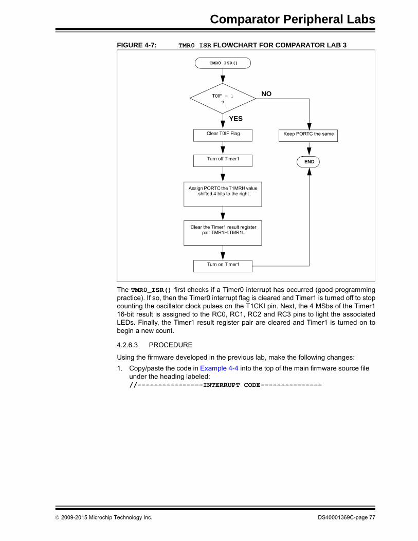
Comparator Peripheral Labs
FIGURE 4-7: TMR0_ISR FLOWCHART FOR COMPARATOR LAB 3
The TMR0_ISR() first checks if a Timer0 interrupt has occurred (good programmingpractice). If so, then the Timer0 interrupt flag is cleared and Timer1 is turned off to stopcounting the oscillator clock pulses on the T1CKI pin. Next, the 4 MSbs of the Timer116-bit result is assigned to the RC0, RC1, RC2 and RC3 pins to light the associatedLEDs. Finally, the Timer1 result register pair are cleared and Timer1 is turned on tobegin a new count.
4.2.6.3 PROCEDURE
Using the firmware developed in the previous lab, make the following changes:
1. Copy/paste the code in Example 4-4 into the top of the main firmware source fileunder the heading labeled://----------------INTERRUPT CODE---------------
END
TMR0_ISR()
T0IF = 1
?
Clear T0IF Flag
Turn off Timer1
Assign PORTC the T1MRH value shifted 4 bits to the right
Clear the Timer1 result register pair TMR1H:TMR1L
Turn on Timer1
YES
NO
Keep PORTC the same
2009-2015 Microchip Technology Inc. DS40001369C-page 77

PICDEMTM Lab Development Board User’s Guide
EXAMPLE 4-4: TMR0_ISR CODE FOR LAB 3
2. Copy and paste the code in Example 4-5 into the Initialize() over the codefrom the previous lab:
void interrupt TMR0_ISR(void)
//Check if Timer0 interrupt has occurred
if(T0IE&&T0IF)
//if so, clear the interrupt flagT0IF = 0;//Turn off Timer1 (stop counting)TMR1ON = 0;//Assign the upper 4-bits of the 16-bit//result to PORTC to light the LEDs connected//RC0,R1,RC2 and RC3PORTC = TMR1H>>4;TMR0 = 10;//Clear the Timer1 register pairTMR1L = 0;TMR1H = 0;//Turn Timer1 back to start counting againTMR1ON = 1;
else PORTC = PORTC;
DS40001369C-page 78 2009-2015 Microchip Technology Inc.
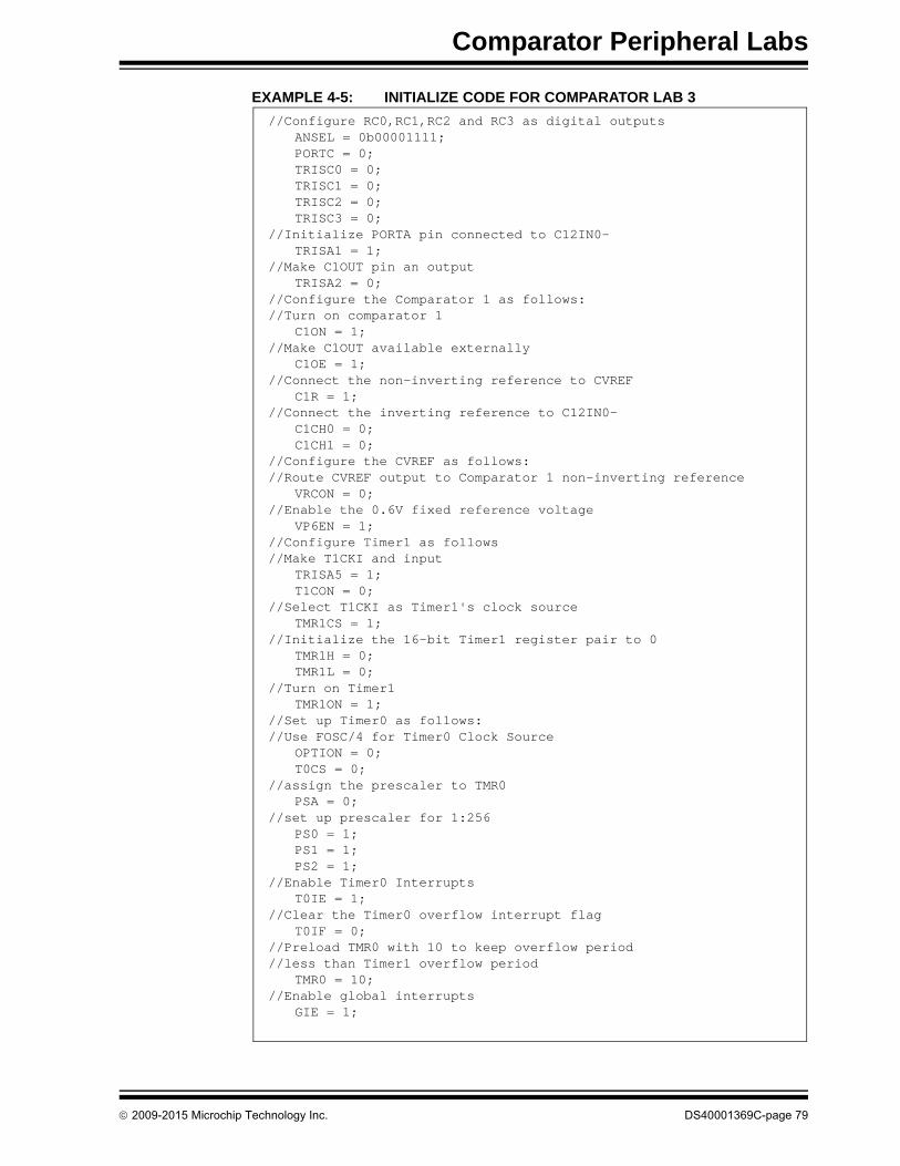
Comparator Peripheral Labs
EXAMPLE 4-5: INITIALIZE CODE FOR COMPARATOR LAB 3
//Configure RC0,RC1,RC2 and RC3 as digital outputsANSEL = 0b00001111;PORTC = 0;TRISC0 = 0;TRISC1 = 0;TRISC2 = 0;TRISC3 = 0;
//Initialize PORTA pin connected to C12IN0-TRISA1 = 1;
//Make C1OUT pin an outputTRISA2 = 0;
//Configure the Comparator 1 as follows://Turn on comparator 1
C1ON = 1;//Make C1OUT available externally
C1OE = 1;//Connect the non-inverting reference to CVREF
C1R = 1;//Connect the inverting reference to C12IN0-
C1CH0 = 0;C1CH1 = 0;
//Configure the CVREF as follows://Route CVREF output to Comparator 1 non-inverting reference
VRCON = 0;//Enable the 0.6V fixed reference voltage
VP6EN = 1;//Configure Timer1 as follows//Make T1CKI and input
TRISA5 = 1;T1CON = 0;
//Select T1CKI as Timer1's clock sourceTMR1CS = 1;
//Initialize the 16-bit Timer1 register pair to 0TMR1H = 0;TMR1L = 0;
//Turn on Timer1TMR1ON = 1;
//Set up Timer0 as follows://Use FOSC/4 for Timer0 Clock Source
OPTION = 0;T0CS = 0;
//assign the prescaler to TMR0PSA = 0;
//set up prescaler for 1:256PS0 = 1;PS1 = 1;PS2 = 1;
//Enable Timer0 InterruptsT0IE = 1;
//Clear the Timer0 overflow interrupt flagT0IF = 0;
//Preload TMR0 with 10 to keep overflow period//less than Timer1 overflow period
TMR0 = 10;//Enable global interrupts
GIE = 1;
2009-2015 Microchip Technology Inc. DS40001369C-page 79

PICDEMTM Lab Development Board User’s Guide
3. Copy and paste the code in Example 4-6 into the main() over the code fromthe previous lab:
EXAMPLE 4-6: MAIN() CODE FOR COMPARATOR LAB 3
4. Compile the project. There should be no errors.
4.2.6.4 TESTING THE APPLICATION
Program the PIC16F690. Adjust the R1 potentiometer until the LEDs begin to lightdisplaying a binary value. Touching the thermistor should introduce heat, reduce thefrequency of oscillation and increase the binary count on the LED display. Introducingcold to the thermistor should have the opposite effect thereby decreasing the binarycount.
The solution for this project is located in the C:\PICDEM_Lab\Comparator_Lab\Comparator_Lab3\solution directory.
Initialize(); //Initialize the relevant registerswhile(1);
DS40001369C-page 80 2009-2015 Microchip Technology Inc.

PICDEMTM LAB DEVELOPMENT
BOARD USER’S GUIDEChapter 5. Analog-to-Digital Converter Peripheral Labs
5.1 INTRODUCTION
The Analog-to-Digital Converter (ADC) peripheral allows conversion of an analog inputsignal to a 10-bit binary value representing that signal so that it can be used in firmware.
The following labs cover some of the fundamental features of the Analog-to-DigitalConverter (ADC) peripheral found on the PIC16F690 including some uniqueapplications.
5.2 ADC LABS
The labs that will be implemented in this chapter are:
• Lab 1: Simple ADC
• Lab 2: Audible Temperature Sensor
5.2.1 Reference Documentation
All documentation is available on the PICDEM™ Lab Development Kit accompanyingCD-ROM
• PIC16F690 Data Sheet (DS41262)
- Section 4: I/O Ports
- Section 5: Timer0 Module
- Section 9: Analog-to-Digital Converter (ADC) Module
• Timers: Timer0 Tutorial (Part 1) (DS51628)
• Timers: Timer0 Tutorial (Part 2) (DS51702)
• Introduction to MPLAB IDE and HI-TECH C PRO for the PIC10/12/16 MCUFamily Lite Mode Compiler Tutorial (DS41322)
5.2.2 Equipment Required
To complete the labs in this section, the following components are required:
1. 1 – 100 resistor
2. 4 – 470resistors
3. 1 – 1 kresistor
4. 1 – 10 kresistor
5. 1 – 100 kpotentiometer
6. 1 – 10 kNTC Thermistor
7. 4 – Light Emitting Diodes
8. 1 – IRFD010 N-Channel MOSFET
9. PIC16F690 populating socket U2
10. Assorted jumper wires
2009-2015 Microchip Technology Inc. DS40001369C-page 81
PICDEMTM Lab Development Board User’s Guide
5.2.3 Lab 1: Simple ADC
5.2.3.1 NEW REGISTERS USED IN THIS LAB
To configure the peripherals used in this lab, the following registers are used:
1. ADC Control Register 0: ADCON0 (Register 9-1 in Section 9 of the PIC16F690Data Sheet)
- Configures ADC conversion result justification.
- Select ADC reference voltage.
- Selects ADC input channel (i.e., pin with analog voltage to be converted).
- Starts ADC conversion and determines when ADC conversion is complete.
- Enables the ADC peripheral.
2. ADC Control Register 1: ADCON1 (Register 9-2 in Section 9 of the PIC16F690Data Sheet)
- Determines ADC conversion clock.
3. ADC Result Register high: ADRESH (see Register 9-3 in Section 9 of thePIC16F690 Data Sheet)
- Holds upper eight bits or upper two bits (depending on justification selected)of 10-bit ADC conversion result.
4. ADC Result Register low: ADRESL (see Register 9-4 in Section 9 of thePIC16F690 Data Sheet)
- Holds lower eight bits or lower two bit (depending on justification selected) of10-bit ADC conversion result.
5.2.3.2 OVERVIEW
In this lab, the ADC peripheral on the PIC16F690 is used to perform a simpleconversion of an analog voltage present on pin 13. The voltage is varied using a100 k potentiometer. This voltage is compared against a reference voltage togenerate a 10-bit binary result via successive approximation stored into two 8-bit ADCresult registers ADRESH and ADRESL. The ADC result is software selectable as eitherleft or right justified as shown in Section 9.1.6 of the PIC16F690 Data Sheet. Thisapplication will configure the ADC result as left justified with the four Most Significantbits of the 10-bit result output to the RC0, RC1, RC2 and RC3 PORTC pins used to lightconnected LEDs accordingly.The PICDEM™ Development Board configurationschematic is shown in Figure 5-1.
DS40001369C-page 82 2009-2015 Microchip Technology Inc.
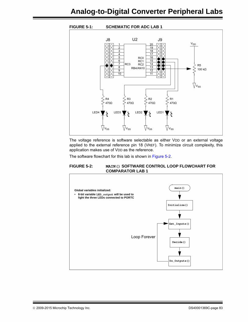
Analog-to-Digital Converter Peripheral Labs
FIGURE 5-1: SCHEMATIC FOR ADC LAB 1
The voltage reference is software selectable as either VDD or an external voltageapplied to the external reference pin 18 (VREF). To minimize circuit complexity, thisapplication makes use of VDD as the reference.
The software flowchart for this lab is shown in Figure 5-2.
FIGURE 5-2: MAIN() SOFTWARE CONTROL LOOP FLOWCHART FOR COMPARATOR LAB 1
12345678910
20191817161514131211
J9J8
R3
470Ω
LED3
VDD
R5
100 kΩ
VSS
VSS
RB4/AN10
U2
RC0RC1RC2RC3
R2
470Ω
LED2
VSS
R1
470Ω
LED1
VSS
R4
470Ω
LED4
VSS
main()
Initialize()
Loop Forever
Get_Inputs()
Decide()
Do_Outputs()
Global variables initialized:
• 8-bit variable LED_output will be used to light the three LEDs connected to PORTC
2009-2015 Microchip Technology Inc. DS40001369C-page 83

PICDEMTM Lab Development Board User’s Guide
The Initialize() configures the peripherals as follows:
• Ports
- Configure pin 13 as an analog input (using TRISB4).
- Clear the PORTC register.
- Configure RC0, RC1, RC2 and RC3 pins as digital output.
• ADC
- Select ADC conversion clock FRC.
- Configure voltage reference using VDD.
- Select channel 10 as the ADC input channel (Pin 13: RB4/AN10).
- Select result format left justified (10-bit result in ADRESH<7:0> andADRESL<7:6>).
- Turn on ADC module.
Next, the Get_Inputs() performs an ADC on the voltage present on pin 13. Theinternal capacitor connected to the input of the ADC peripheral needs time to charge tothe voltage present on the pin. Therefore, software will need to implement a short delayto allow for this charging time. The ADC module section “A/D AcquisitionRequirements” of the data sheet goes into great detail and includes an equation forselecting an appropriate acquisition time. For the purposes of this lab, a simple 1 mSdelay should be more than sufficient. These parameters become important inhigh-speed applications where every S counts.
The GO/DONE bit in ADCON0 is used to start the ADC process when set to ‘1’. Thisbit also serves as a flag that indicates when the ADC is completed (GO/DONE = 0).Therefore, the Get_Inputs() initiates an ADC by setting GO/DONE then sits andwaits for the bit to clear, indicating a completed conversion.
The software flowchart for the Get_Inputs() is shown in Figure 5-3.
Note: The ADC conversion clock is the time that will be used to convert the analogvoltage present on pin 13 to a 10-bit value in the ADRESH:ADRESLregisters. It takes 11 of these conversion clock cycles to perform a completeADC. If the conversion clock period is insufficient, an incomplete ADC resultwill occur. The electrical specifications for the PIC16F690 state that theconversion clock must have a period of at least 1.5 Seconds or afrequency of approximately 667 kHz. The ADC module section of the datasheet specifies acceptable conversion clock frequencies depending on themain oscillator used to drive the microcontroller and should be referenced.In this application, a dedicated internal oscillator for the ADC module isused ensuring a conversion clock frequency of between 2-6 Seconds.(see Table 17-16 in Section 17 of the PIC16F690 Data Sheet).
DS40001369C-page 84 2009-2015 Microchip Technology Inc.

Analog-to-Digital Converter Peripheral Labs
FIGURE 5-3: MAIN() SOFTWARE CONTROL LOOP FLOWCHART FOR COMPARATOR LAB 1
Following the Get_Inputs(), the 10-bit ADC result is now in the ADRESH:ADRESLregisters. The Decide() assigns the ADC result value, shifted four bit positions to theright, to the LED_Output variable.
Finally, the Do_Outputs() assigns the contents of LED_Output to the PORTCregister that will light the LEDs connected to RC0, RC1, RC2 and RC3 accordingly.
5.2.3.3 PROCEDURE
Using the Project Wizard, create a new project called ADC_Lab1.mcp. Oncecompleted, open the ADC_Lab1.c source file in MPLAB and make the followingchanges:
1. Copy and paste the code in Example 5-1 into the top of the main firmware sourcefile under the heading labeled://----------------DATA MEMORY---------------
EXAMPLE 5-1: GLOBAL VARIABLES USED IN LAB 1
2. Copy and paste the code in Example 5-2 into the top of the main firmware sourcefile under the heading labeled://----------------SUPPORT ROUTINES---------------
Get_Inputs()
Delay_1mS()
Start conversion by setting GO/DONE bit
Gives ADC capacitor time to charge
NO
GO/DONE = 1
?
YES
END
Wait for ADC to complete
unsigned char LED_Output = 0;//assigned to PORTC to light //connected LEDs
2009-2015 Microchip Technology Inc. DS40001369C-page 85

PICDEMTM Lab Development Board User’s Guide
EXAMPLE 5-2: DELAY_1MS() CODE FOR ADC LAB 1
3. Copy and paste the code in Example 5-3 into the Initialize() sectionlabeled://ADD INITIALIZE CODE HERE
/*---------------------------------------------------------Subroutine: Delay_1mSParameters: noneReturns:nothingSynopsys:Creates a 1mS delay when called
---------------------------------------------------------*/void Delay_1mS(void)
unsigned int delay_var = 98;//Keep looping until the delay_var is // equal to zero (should take 1mS)while(--delay_var);
DS40001369C-page 86 2009-2015 Microchip Technology Inc.

Analog-to-Digital Converter Peripheral Labs
EXAMPLE 5-3: INITIALIZE CODE FOR COMPARATOR LAB 1
4. Copy and paste the code in Example 5-4 into the Get_Inputs() sectionlabeled://ADD GET INPUTS CODE HERE
//Configure Port://Disable pin output driver (See TRIS register)TRISB4 = 1;
// Configure pin as analogANS10 = 1;
//Configure RC0, RC1, RC2 and RC3 as digital outputPORTC = 0;TRISC0 = 0;TRISC1 = 0;TRISC2 = 0;TRISC3 = 0;
ANS4 = 0;ANS5 = 0;ANS6 = 0;ANS7 = 0;
//Configure the ADC module://Select ADC conversion clock FrcADCS0 = 1;ADCS1 = 1;ADCS2 = 1;
//Configure voltage reference using VDDVCFG = 0;
//Select ADC input channel Pin 13 (RB4/AN10)CHS0 = 0;CHS1 = 1;CHS2 = 0;CHS3 = 1;
//Select result format left justifiedADFM = 0;
//Turn on ADC moduleADON = 1;
2009-2015 Microchip Technology Inc. DS40001369C-page 87

PICDEMTM Lab Development Board User’s Guide
EXAMPLE 5-4: GET_INPUTS() CODE FOR ADC LAB 1
5. Copy and paste the code in Example 5-5 into the Decide() section labeled://ADD DECIDE CODE HERE
EXAMPLE 5-5: DECIDE() CODE FOR ADC LAB 1
6. Copy and paste the code in Example 5-6 into the Do_Outputs() sectionlabeled://ADD DO OUTPUTS CODE HERE
EXAMPLE 5-6: D0_OUTPUTS() CODE FOR ADC LAB 1
7. Copy and paste the code in Example 5-7 into the main() section labeled://ADD MAIN CODE HERE
EXAMPLE 5-7: MAIN() CODE FOR ADC LAB 1
8. Compile the project. There should be no errors.
//Perform an ADC of potentiometer connected to pin 13
//Wait the required acquisition timeDelay_1mS();
//Start conversion by setting the GO/DONE bit.GODONE = 1;
//Wait for ADC conversion to complete //Polling the GO/DONE bit// 0 = ADC completed// 1 = ADC in progresswhile(GODONE == 1);
//Assign the upper 4 bits of ADRESH to the lower 4 bits//of LED_OutputLED_Output = ADRESH >> 4; //Shifts the bits in ADRESL 4 bits
//to the right
//Assign contents of LED_Output to PORTC to light the connected//LEDsPORTC = LED_Output;
Initialize(); //Initialize the relevant registerswhile(1)
Get_Inputs();Decide();Do_Outputs();
DS40001369C-page 88 2009-2015 Microchip Technology Inc.
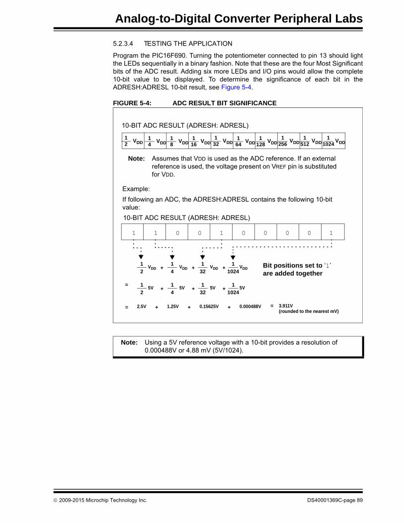
Analog-to-Digital Converter Peripheral Labs
5.2.3.4 TESTING THE APPLICATION
Program the PIC16F690. Turning the potentiometer connected to pin 13 should lightthe LEDs sequentially in a binary fashion. Note that these are the four Most Significantbits of the ADC result. Adding six more LEDs and I/O pins would allow the complete10-bit value to be displayed. To determine the significance of each bit in theADRESH:ADRESL 10-bit result, see Figure 5-4.
FIGURE 5-4: ADC RESULT BIT SIGNIFICANCE
VDD12
VDD14
VDD18
VDD1
16VDD
132
VDD1
64VDD
1128
VDD1
256VDD
1512
VDD1
1024
10-BIT ADC RESULT (ADRESH: ADRESL)
Example:
If following an ADC, the ADRESH:ADRESL contains the following 10-bit value:
10-BIT ADC RESULT (ADRESH: ADRESL)
1 1 0 0 1 0 0 0 0 1
VDD2
1+ VDD
4
1+ VDD
32
1+ VDD
1024
1
=5V
2
1+ 5V
4
1+ 5V
32
1+ 5V
1024
1
= 2.5V + 1.25V + 0.15625V + 0.000488V = 3.911V (rounded to the nearest mV)
Note: Assumes that VDD is used as the ADC reference. If an external reference is used, the voltage present on VREF pin is substituted for VDD.
Bit positions set to ‘1’ are added together
Note: Using a 5V reference voltage with a 10-bit provides a resolution of 0.000488V or 4.88 mV (5V/1024).
2009-2015 Microchip Technology Inc. DS40001369C-page 89

PICDEMTM Lab Development Board User’s Guide
Since this lab outputs the four Most Significant bits of the ADC result and VDD is usedas the reference voltage, the LED display should correspond with the following voltagelevels shown in Table 5-1.
The solution for this project is located in the C:\PICDEM_Lab\ADC_Labs\ADC_Lab1\solution directory.
TABLE 5-1: CORRESPONDING VOLTAGE ON PIN 13 RELATED TO LIT LEDS (1 = LED ON, 0 = LED OFF)
LED4 LED3 LED2 LED1 pin 13 Voltage
0 0 0 0 < 0.3125V
0 0 0 1 > 0.3125V
0 0 1 0 > 0.625V
0 0 1 1 > 0.9375V
0 1 0 0 > 1.25V
0 1 0 1 > 1.5625V
0 1 1 0 > 1.875V
0 1 1 1 > 2.1875V
1 0 0 0 > 2.5V
1 0 0 1 > 2.8125V
1 0 1 0 > 3.125V
1 0 1 1 > 3.4375V
1 1 0 0 > 3.75V
1 1 0 1 > 4.0625V
1 1 1 0 > 4.375V
1 1 1 1 > 4.6875V or greater
Note: The greater than symbol (>) is required since the lower six bits of the ADC result are not shown using LEDs.
DS40001369C-page 90 2009-2015 Microchip Technology Inc.
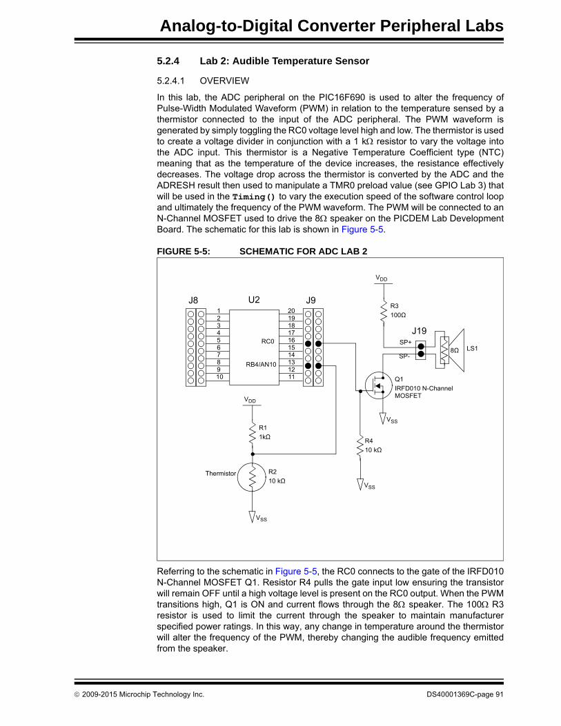
Analog-to-Digital Converter Peripheral Labs
5.2.4 Lab 2: Audible Temperature Sensor
5.2.4.1 OVERVIEW
In this lab, the ADC peripheral on the PIC16F690 is used to alter the frequency ofPulse-Width Modulated Waveform (PWM) in relation to the temperature sensed by athermistor connected to the input of the ADC peripheral. The PWM waveform isgenerated by simply toggling the RC0 voltage level high and low. The thermistor is usedto create a voltage divider in conjunction with a 1 kresistor to vary the voltage intothe ADC input. This thermistor is a Negative Temperature Coefficient type (NTC)meaning that as the temperature of the device increases, the resistance effectivelydecreases. The voltage drop across the thermistor is converted by the ADC and theADRESH result then used to manipulate a TMR0 preload value (see GPIO Lab 3) thatwill be used in the Timing() to vary the execution speed of the software control loopand ultimately the frequency of the PWM waveform. The PWM will be connected to anN-Channel MOSFET used to drive the 8speaker on the PICDEM Lab DevelopmentBoard. The schematic for this lab is shown in Figure 5-5.
FIGURE 5-5: SCHEMATIC FOR ADC LAB 2
Referring to the schematic in Figure 5-5, the RC0 connects to the gate of the IRFD010N-Channel MOSFET Q1. Resistor R4 pulls the gate input low ensuring the transistorwill remain OFF until a high voltage level is present on the RC0 output. When the PWMtransitions high, Q1 is ON and current flows through the 8speaker. The 100 R3resistor is used to limit the current through the speaker to maintain manufacturerspecified power ratings. In this way, any change in temperature around the thermistorwill alter the frequency of the PWM, thereby changing the audible frequency emittedfrom the speaker.
12345678910
20191817161514131211
J9J8
VDD
R1
1kΩ
VSS
RB4/AN10
U2
RC0
VSS
VDD
R3
100Ω
8Ω
R2
10 kΩ
J19SP+
SP-LS1
Thermistor
Q1
IRFD010 N-Channel MOSFET
VSS
R4
10 kΩ
2009-2015 Microchip Technology Inc. DS40001369C-page 91

PICDEMTM Lab Development Board User’s Guide
The audible frequency range is between 20-20000Hz. Therefore, the Timing()delays from a maximum of 4.096 mS (244.1 Hz) to a minimum of 1.536 mS (651 Hz).These values are determined using the internal instruction clock (FOSC/4) as the TMR0clock source with a prescaler of 1:16. Other values could easily be used as long as thefrequency of the PWM remains within the audible range.
The software flowchart for this lab is shown in Figure 5-6.
FIGURE 5-6: MAIN() SOFTWARE CONTROL LOOP FLOWCHART FOR ADC LAB 2
The Initialize() configures the peripherals as follows:
• Ports
- Clear PORTB.
- Configure pin 13 as an analog input (using TRISB4).
- Clear the PORTC register.
- Configure RC0 pin as digital output.
• Timer0
- Select the FOSC/4 internal instruction clock as the Timer0 clock source.
- Increment TMR0 on the low-to-high transition of FOSC/4.
- Assign the prescaler to Timer0 and configure at a rate of 1:16.
• ADC
- Select ADC conversion clock FRC.
- Configure voltage reference using VDD.
- Select channel 10 as the ADC input channel (Pin 13: RB4/AN10).
- Select result format left justified (10-bit result in ADRESH<7:0> and ADRESL<7:6>).
- Turn on ADC module.
main()
Initialize()
Loop Forever
Get_Inputs()
Decide()
Do_Outputs()
Global variables initialized:
• 8-bit variable TMR0_preload will be used to vary the delay in Timing() to alter the frequency of the PWM output on RC0
Timing()
DS40001369C-page 92 2009-2015 Microchip Technology Inc.

Analog-to-Digital Converter Peripheral Labs
Next, the Get_Inputs() performs an ADC on the voltage present on pin 13 using thesame code as Lab 1 with one minor change. This application is very dependent on thetiming of the software control loop. The 1mS delay used in Lab 1 to allow the holdcapacitor on the input of ADC to fully charge to the pin voltage is excessive. Using theexample given in Equation 9-1, Section 9 in the PIC16F690 Data Sheet as a reference,the acquisition delay time is shortened to 8 S which should be sufficient.
The Decide() assigns the ADC result value, shifted three bit positions to the left, tothe TMR0_preload variable.
The Do_Outputs() assigns the current toggle bit value to RC0 that will transitionthe output accordingly.
Finally, the Timing() clears the TMR0 overflow flag (T0IF), preloads the TMR0register with the TMR0_preload value subtracted from 255. The function then waitsuntil the T0IF is set high before returning to the main(). In this way, as the temperatureat the thermistor increases, as will the frequency of the PWM.
5.2.4.2 PROCEDURE
Using the firmware developed in the previous lab, make the following changes:
1. Copy/paste the code in Example 5-8 into the top of the main firmware source fileunder the heading labeled://----------------DATA MEMORY---------------
EXAMPLE 5-8: GLOBAL VARIABLES USE IN ADC LAB 2
2. Copy and paste the code in Example 5-9 over the Initialize() code fromthe previous lab:
Note: Be sure to paste over the code from the previous lab.
unsigned char LED_Output = 0; //assigned to PORTC to light //connected LEDs
bit toggle = 0;//Used to generate waveform on RC0
unsigned char TMR0_preload = 0; //Varied by ADRESH to change //frequency of
//waveform on RC0
2009-2015 Microchip Technology Inc. DS40001369C-page 93

PICDEMTM Lab Development Board User’s Guide
EXAMPLE 5-9: INITIALIZE CODE FOR ADC LAB 2
3. Copy and paste the code in Example 5-10 over the Get_Inputs() code fromthe previous lab:
//Configure Port:PORTB = 0;//Disable pin output driver (See TRIS register)TRISB4 = 1;
// Configure RB4 as analog pin as analogANS10 = 1;
//Configure RC0, RC1, RC2 and RC3 as digital outputPORTC = 0;TRISC0 = 0;ANS4 = 0;
//Configure Timer0 as follows:
//Select the FOSC/4 internal instruction clock//as the clock source for TMR0T0CS = 0;//Increment TMR0 value on low-to-high transition//of the FOSC/4T0SE = 0;//Assign the prescaler to TMR0PSA = 1;//Configure the prescaler to increment TMR0//at a rate of 1:16PS0 = 1;PS1 = 1;PS2 = 0;
//Configure the ADC module://Select ADC conversion clock FrcADCS0 = 1;ADCS1 = 1;ADCS2 = 1;
//Configure voltage reference using VDDVCFG = 0;
//Select ADC input channel Pin 13 (RB4/AN10)CHS0 = 0;CHS1 = 1;CHS2 = 0;CHS3 = 1;
//Select result format left justifiedADFM = 0;
//Turn on ADC moduleADON = 1;
DS40001369C-page 94 2009-2015 Microchip Technology Inc.
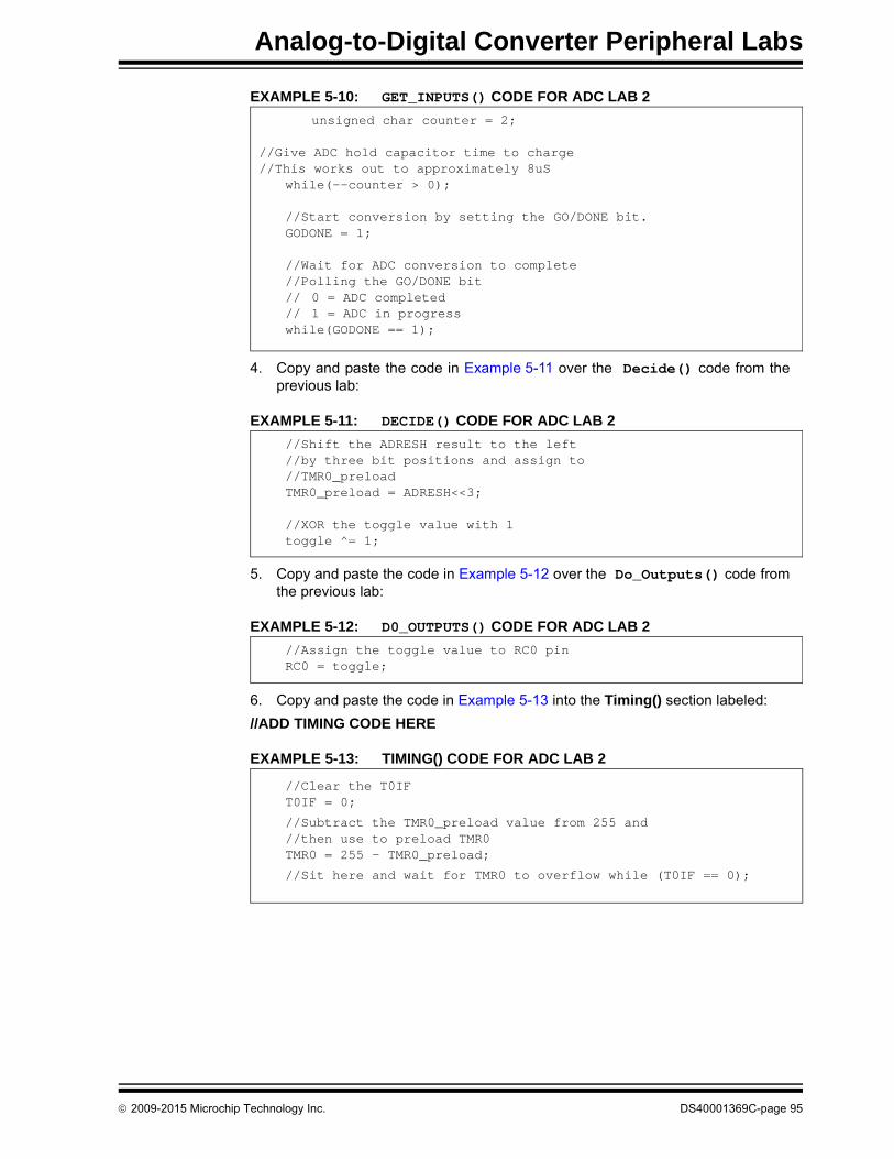
Analog-to-Digital Converter Peripheral Labs
EXAMPLE 5-10: GET_INPUTS() CODE FOR ADC LAB 2
4. Copy and paste the code in Example 5-11 over the Decide() code from theprevious lab:
EXAMPLE 5-11: DECIDE() CODE FOR ADC LAB 2
5. Copy and paste the code in Example 5-12 over the Do_Outputs() code fromthe previous lab:
EXAMPLE 5-12: D0_OUTPUTS() CODE FOR ADC LAB 2
6. Copy and paste the code in Example 5-13 into the Timing() section labeled:
//ADD TIMING CODE HERE
EXAMPLE 5-13: TIMING() CODE FOR ADC LAB 2
unsigned char counter = 2;
//Give ADC hold capacitor time to charge//This works out to approximately 8uS
while(--counter > 0);
//Start conversion by setting the GO/DONE bit.GODONE = 1;
//Wait for ADC conversion to complete //Polling the GO/DONE bit// 0 = ADC completed// 1 = ADC in progresswhile(GODONE == 1);
//Shift the ADRESH result to the left//by three bit positions and assign to //TMR0_preloadTMR0_preload = ADRESH<<3;
//XOR the toggle value with 1toggle ^= 1;
//Assign the toggle value to RC0 pinRC0 = toggle;
//Clear the T0IFT0IF = 0;
//Subtract the TMR0_preload value from 255 and //then use to preload TMR0TMR0 = 255 – TMR0_preload;
//Sit here and wait for TMR0 to overflow while (T0IF == 0);
2009-2015 Microchip Technology Inc. DS40001369C-page 95

PICDEMTM Lab Development Board User’s Guide
7. Copy and paste the code in Example 5-14 over the main() code from theprevious lab:
EXAMPLE 5-14: MAIN() CODE FOR ADC LAB 2
8. Compile the project. There should be no errors.
5.2.4.3 TESTING THE APPLICATION
Program the PIC16F690. An audible tone should emit from the speaker. Pinching thethermistor should introduce body heat to the component, thereby increasing thefrequency of the speaker output. Colder temperature sources applied to the thermistorshould reduce the speaker output frequency.
The solution for this project is located in the C:\PICDEM_Lab\ADC_Labs\ADC_Lab2\solution directory.
Initialize(); //Initialize the relevant registerswhile(1)
Get_Inputs();Decide();Do_Outputs();Timing();
DS40001369C-page 96 2009-2015 Microchip Technology Inc.
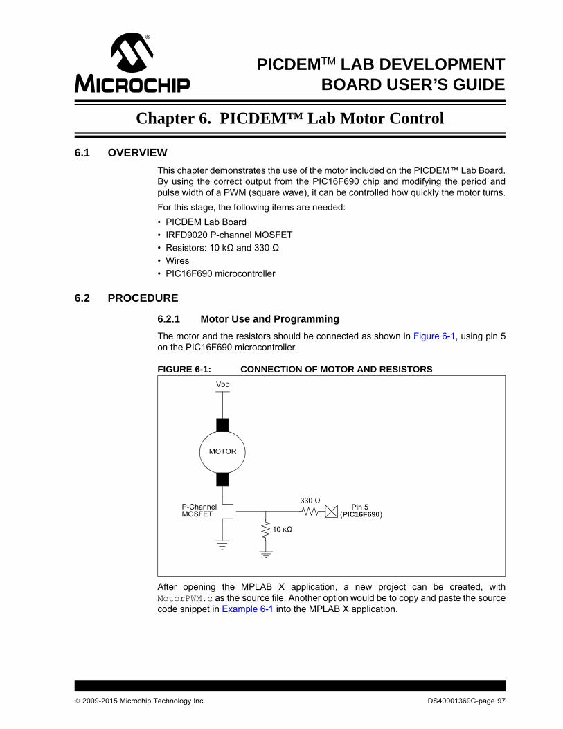
PICDEMTM LAB DEVELOPMENT
BOARD USER’S GUIDEChapter 6. PICDEM™ Lab Motor Control
6.1 OVERVIEW
This chapter demonstrates the use of the motor included on the PICDEM™ Lab Board.By using the correct output from the PIC16F690 chip and modifying the period andpulse width of a PWM (square wave), it can be controlled how quickly the motor turns.
For this stage, the following items are needed:
• PICDEM Lab Board
• IRFD9020 P-channel MOSFET
• Resistors: 10 kΩ and 330 Ω
• Wires
• PIC16F690 microcontroller
6.2 PROCEDURE
6.2.1 Motor Use and Programming
The motor and the resistors should be connected as shown in Figure 6-1, using pin 5on the PIC16F690 microcontroller.
FIGURE 6-1: CONNECTION OF MOTOR AND RESISTORS
After opening the MPLAB X application, a new project can be created, withMotorPWM.c as the source file. Another option would be to copy and paste the sourcecode snippet in Example 6-1 into the MPLAB X application.
VDD
MOTOR
P-ChannelMOSFET
Pin 5(PIC16F690)
330 Ω
10 KΩ
2009-2015 Microchip Technology Inc. DS40001369C-page 97

PICDEMTM Lab Development Board User’s Guide
EXAMPLE 6-1: SOURCE CODE SNIPPET
6.2.2 PWM Period
The formula for the period of the pulse-width modulator (PWM) can be found in“PIC16F631/677/685/687/689/690 Data Sheet 20-Pin Flash-Based, 8-Bit CMOSMicrocontrollers with nanoWatt Technology” (DS41262), Section 11.3.1. A part of thissection has been included below.
6.2.2.1 PWM PERIOD
The PWM period is specified by the PR2 register of Timer2. The PWM period can becalculated using the formula in Equation 6-1.
EQUATION 6-1: PWM PERIOD
#include <pic.h>
// #pragma config statements should precede project file includes.// Use project enums instead of #define for ON and OFF.
// CONFIG#pragma config FOSC = EXTRCCLK // Oscillator Selection bits (RC oscillator: CLKOUT function on RA4/OSC2/CLKOUT pin, RC on RA5/OSC1/CLKIN)#pragma config WDTE = ON // Watchdog Timer Enable bit (WDT enabled)#pragma config PWRTE = OFF // Power-up Timer Enable bit (PWRT disabled)#pragma config MCLRE = ON // MCLR Pin Function Select bit (MCLR pin function is MCLR)#pragma config CP = OFF // Code Protection bit (Program memory code protection is disabled)#pragma config CPD = OFF // Data Code Protection bit (Data memory code protection is disabled)#pragma config BOREN = ON // Brown-out Reset Selection bits (BOR enabled)#pragma config IESO = ON // Internal External Switchover bit (Internal External Switchover mode is enabled)#pragma config FCMEN = ON // Fail-Safe Clock Monitor Enabled bit (Fail-Safe Clock Monitor is enabled)
//-----------------------------------------------------------------------------
//-----------------------------------------------------------------------------main()OSCCON = 0b00101111; // Osc is set to 2 MHzTRISC = 0b00100000; // bit 5 = 1 temp disables PORTC RC5/CCP1 on PIC16F690PORTC = 0b00000000; // Clear PortC portPR2 = 124; // sets the period or PWM frequency to 4 kHz (0.25 ms)T2CON = 0b00000100; // sets postscaler and prescaler to 1
// These two registers determine the pulse width (CCPR1L:CCP1CON<5:4>)CCPR1L = 0b00111110;CCP1CON = 0b00101111;
TRISC = 0b00000000; // bit 5 = 0 enable output PORTC TRIS RC5/CCP1 ECCP high
while(1);
PWM Period PR2 1+ 4 TOSC =
(TMR2 Prescale Value)
Note: TOSC = 1/FOSC
DS40001369C-page 98 2009-2015 Microchip Technology Inc.
PICDEM™ Lab Motor Control
When TMR2 is equal to PR2, the following three events occur on the next increment cycle:
• TMR2 is cleared
• The CCP1 pin is set. (Exception: If the PWM duty cycle = 0%, the pin will not be set.)
• The PWM duty cycle is latched from CCPR1L into CCPR1H.
EQUATION 6-2: PULSE WIDTH
EQUATION 6-3: DUTY CYCLE RATIO
The CCPR1H register and a 2-bit internal latch are used to double buffer the PWM duty cycle.The double buffering is essential for a glitchless PWM operation.
The 8-bit timer TMR2 register is concatenated with either the 2-bit internal system clock (FOSC) orwith the two bits of the prescaler, to create the 10-bit time base. The system clock is used if theTimer2 prescaler is set to 1:1.
When the 10-bit time base matches the CCPR1H and 2-bit latch, then the CCP1 pin is cleared.
As indicated in Example 6-1 that includes the code snippet, the oscillator frequency has beenset to 2 MHz. By setting PR2 to 124, the period set out is 4 kHz.
EQUATION 6-1: PWM PERIOD
The duty cycle is set by a combination of the registers in CCPR1L and CCP1CON. Ituses all eight registers from CCPR1L and registers 4 and 5 from CCP1CON.
For example, in the beginning the duty cycle is 50% (half the period). Hence, the valuein the equation for pulse width needs to be 250. In binary, 250 is 11111010, the twoLeast Significant bits go into registers 5 and 4 in CCP1CON, while the remaining bitsgo into CCPR1L.
EQUATION 6-2: 50% DUTY CYCLE AND PULSE WIDTH
Note: The Timer2 postscaler is not used in the determination of the PWM frequency.
Pulse Width CCPR1L:CCP1CON<5:4> =
TOSC (TMR2 Prescale Value)
Duty Cycle RatioCCPR1L:CCP1CON<5:4>
4 PR2 1+ -----------------------------------------------------------------------=
PWM Period 124 1+ 4 12000000--------------------- 1 .00025s = =
1.00025---------------- 4000 Hz=
50% Duty Cycle: Period
2------------------
.00025s2
------------------- .000125s= =
PulseWidth ???1
2000000--------------------- 0.000125s= =
.000125 2000000 250=
2009-2015 Microchip Technology Inc. DS40001369C-page 99
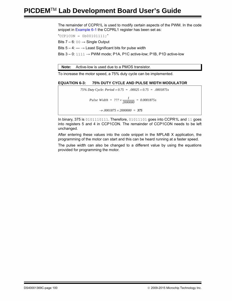
PICDEMTM Lab Development Board User’s Guide
The remainder of CCPR1L is used to modify certain aspects of the PWM. In the codesnippet in Example 6-1 the CCPRL1 register has been set as:
“CCP1CON = 0b00101111;”
Bits 7 – 6: 00 → Single Output
Bits 5 – 4: — → Least Significant bits for pulse width
Bits 3 – 0: 1111 → PWM mode; P1A, P1C active-low; P1B, P1D active-low
To increase the motor speed, a 75% duty cycle can be implemented.
EQUATION 6-3: 75% DUTY CYCLE AND PULSE WIDTH MODULATOR
In binary, 375 is 0101110111. Therefore, 01011101 goes into CCPR1L and 11 goesinto registers 5 and 4 in CCP1CON. The remainder of CCP1CON needs to be leftunchanged.
After entering these values into the code snippet in the MPLAB X application, theprogramming of the motor can start and this can be heard running at a faster speed.
The pulse width can also be changed to a different value by using the equationsprovided for programming the motor.
Note: Active-low is used due to a PMOS transistor.
75% Duty Cycle: Period 0.75 .00025 0.75 .0001875s= =
Pulse Width ???1
2000000--------------------- 0.0001875s= =
.0001875 2000000 375=
DS40001369C-page 100 2009-2015 Microchip Technology Inc.

PICDEMTM LAB DEVELOPMENT
BOARD USER’S GUIDEAppendix A. Schematic
A.1 PICDEM™ LAB DEVELOPMENT KIT SCHEMATICJ1
1J2
DJ00
5B2
D3
S1
V CC
S1G
S1G
VBAT
D5
3
270ΩPWR ON
R5
0.1 UF
D1
C13
1N41
48W
S
D2 U1
LM31
7MST
T3G
INOU
T
OUT
ADJ 1
2 4
D4
R2 330Ω
1N4148WS
C722
UFJ3
J4J5
V DD1
V DD2
V DD3
PICk
it™ S
erial
Hea
der
Pin
I2 C™SP
IUS
ART
1 2 3 4 5 6
_ _
_
+5V
GND
SDA
SCL
_ _
_
CS +5V
GND
SDI
SCK
SDO
TX +5V
GND RX
_ _
__
_ _
PICk
it™ S
erial
J11
Rece
ptica
lJ1
5
1 2 3 4 5 6
VDD
VDD
VPP
GND
ICSP
DAT
ICSP
CLK
1 2 3 4 5 6
ICSP
1J6
1 2 3 4 5 6
J9U2
1 2 3 4 5 6 7 8 9 10
20 19 18 17 16 15 14 13 12 11
8/14
/20p
MCU
V SS
VDD
RA5
RA4
RA3
RC5
RC4
RC3
RC6
RC7
RB7
RA0
RA1
RA2
RC0
RC1
RC2
RB4
RB5
RB6
1 2 3 4 5 6 7 8 9 10
0.1u
F
C2
J81 2 3 4 5 6 7 8 9 10
CW
C6
10uF
R1
CCW
3352
T-1-
102
32
1
J7
2PHDR
Y1
C10
15pF
C11
15pF
32 kH
z
BT1
9V
J26
2PHD
R
VBAT
J14
CDM
G130
08L-
02-N
DJ1
9
1 2 3 4
1 2LS
1
J10
0.1u
F
C41 2 3 4
U5
1 2 3 4
NC VDD
GP2/
T0CK
I/COU
T/FO
SC4
GP1/
ICSP
CLK/
CIN-
BP3/
MCL
R/V P
P
VSS
NC
GP0/
ICSP
DAT/
CIN+
5
PIC10F204_206-I_P
678 5
1 2 3 4
1 2 3 4 5 6
J18
ICSP
3J1
3
VPP
VDD
GND
ICSP
DAT
ICSP
CLK
J17
1 2 3 4 5 6 7 8 9
1 2 3 4 5 6 7 8 9
U3
PIC_18P
RA2
RA3
RA4/
TOCK
I
MCL
R
Vss
RB0/
INT
RB1
RB2
RB3
RA1
RA0
OSC1
/CLK
IN
OSC2
/CLK
OUT
VDD
RB7
RB6
RB5
RB4
18 17 16 15 14 13 12 11 10
C3 0.1u
F
1 2 3 4 5 6 7 8 9
J16
ICSP
2J1
2
1 2 3 4 5 6
VPP
VDD
GND
ICSP
DAT
ICSP
CLK
VPP3
VDD3
ICSP
DAT3
ICSP
CLK3
VPP3
ICSP
DAT3
V DD3
ICSP
CLK3
GP2-
U5
VDD1
VDD2
VDD3
VDD1
ICSP
DAT1
ICSP
CLK1
RA2/
RB2
RC0
RC1
RC2
RB4
RB5
RB6
RA5/
RB5
RA4/
RB4
RA3
RC5
RC4
RC3
RC6
RC7
RB7
VPP1 VD
D1
ICSP
DAT1
ICSP
CLK1
SDO/
RS
SCL/
SCK
SDA/
SDI
CS/T
X
SP-
SP+
CP+
CN-
XT2
XT2
XT1
XT1
RB3
RB2
RB1
RB0
VP
P2
RA4
RA3
RA2
RA1
RA0
OSC1
OSC2
ICSP
DAT2
ICSP
CLK2
U3_R
B5
U3_R
B4
VDD2
VPP2 VDD2
ICSP
DAT2
ICSP
CLK2
2009-2015 Microchip Technology Inc. DS40001369C-page 101

PICDEMTM Lab Development Board User’s Guide
NOTES:
DS40001369C-page 102 2009-2015 Microchip Technology Inc.

2009-2015 Microchip Technology Inc. DS40001369C-page 103
AMERICASCorporate Office2355 West Chandler Blvd.Chandler, AZ 85224-6199Tel: 480-792-7200 Fax: 480-792-7277Technical Support: http://www.microchip.com/supportWeb Address: www.microchip.com
AtlantaDuluth, GA Tel: 678-957-9614 Fax: 678-957-1455
Austin, TXTel: 512-257-3370
BostonWestborough, MA Tel: 774-760-0087 Fax: 774-760-0088
ChicagoItasca, IL Tel: 630-285-0071 Fax: 630-285-0075
ClevelandIndependence, OH Tel: 216-447-0464 Fax: 216-447-0643
DallasAddison, TX Tel: 972-818-7423 Fax: 972-818-2924
DetroitNovi, MI Tel: 248-848-4000
Houston, TX Tel: 281-894-5983
IndianapolisNoblesville, IN Tel: 317-773-8323Fax: 317-773-5453
Los AngelesMission Viejo, CA Tel: 949-462-9523 Fax: 949-462-9608
New York, NY Tel: 631-435-6000
San Jose, CA Tel: 408-735-9110
Canada - TorontoTel: 905-673-0699 Fax: 905-673-6509
ASIA/PACIFICAsia Pacific OfficeSuites 3707-14, 37th FloorTower 6, The GatewayHarbour City, KowloonHong KongTel: 852-2943-5100Fax: 852-2401-3431
Australia - SydneyTel: 61-2-9868-6733Fax: 61-2-9868-6755
China - BeijingTel: 86-10-8569-7000 Fax: 86-10-8528-2104
China - ChengduTel: 86-28-8665-5511Fax: 86-28-8665-7889
China - ChongqingTel: 86-23-8980-9588Fax: 86-23-8980-9500
China - Dongguan
Tel: 86-769-8702-9880
China - HangzhouTel: 86-571-8792-8115 Fax: 86-571-8792-8116
China - Hong Kong SARTel: 852-2943-5100 Fax: 852-2401-3431
China - NanjingTel: 86-25-8473-2460Fax: 86-25-8473-2470
China - QingdaoTel: 86-532-8502-7355Fax: 86-532-8502-7205
China - ShanghaiTel: 86-21-5407-5533 Fax: 86-21-5407-5066
China - ShenyangTel: 86-24-2334-2829Fax: 86-24-2334-2393
China - ShenzhenTel: 86-755-8864-2200 Fax: 86-755-8203-1760
China - WuhanTel: 86-27-5980-5300Fax: 86-27-5980-5118
China - XianTel: 86-29-8833-7252Fax: 86-29-8833-7256
ASIA/PACIFICChina - XiamenTel: 86-592-2388138 Fax: 86-592-2388130
China - ZhuhaiTel: 86-756-3210040 Fax: 86-756-3210049
India - BangaloreTel: 91-80-3090-4444 Fax: 91-80-3090-4123
India - New DelhiTel: 91-11-4160-8631Fax: 91-11-4160-8632
India - PuneTel: 91-20-3019-1500
Japan - OsakaTel: 81-6-6152-7160 Fax: 81-6-6152-9310
Japan - TokyoTel: 81-3-6880- 3770 Fax: 81-3-6880-3771
Korea - DaeguTel: 82-53-744-4301Fax: 82-53-744-4302
Korea - SeoulTel: 82-2-554-7200Fax: 82-2-558-5932 or 82-2-558-5934
Malaysia - Kuala LumpurTel: 60-3-6201-9857Fax: 60-3-6201-9859
Malaysia - PenangTel: 60-4-227-8870Fax: 60-4-227-4068
Philippines - ManilaTel: 63-2-634-9065Fax: 63-2-634-9069
SingaporeTel: 65-6334-8870Fax: 65-6334-8850
Taiwan - Hsin ChuTel: 886-3-5778-366Fax: 886-3-5770-955
Taiwan - KaohsiungTel: 886-7-213-7828
Taiwan - TaipeiTel: 886-2-2508-8600 Fax: 886-2-2508-0102
Thailand - BangkokTel: 66-2-694-1351Fax: 66-2-694-1350
EUROPEAustria - WelsTel: 43-7242-2244-39Fax: 43-7242-2244-393Denmark - CopenhagenTel: 45-4450-2828 Fax: 45-4485-2829
France - ParisTel: 33-1-69-53-63-20 Fax: 33-1-69-30-90-79
Germany - DusseldorfTel: 49-2129-3766400
Germany - MunichTel: 49-89-627-144-0 Fax: 49-89-627-144-44
Germany - PforzheimTel: 49-7231-424750
Italy - Milan Tel: 39-0331-742611 Fax: 39-0331-466781
Italy - VeniceTel: 39-049-7625286
Netherlands - DrunenTel: 31-416-690399 Fax: 31-416-690340
Poland - WarsawTel: 48-22-3325737
Spain - MadridTel: 34-91-708-08-90Fax: 34-91-708-08-91
Sweden - StockholmTel: 46-8-5090-4654
UK - WokinghamTel: 44-118-921-5800Fax: 44-118-921-5820
Worldwide Sales and Service
01/27/15