physics and nanotechnology - probably the best education ... · pdf filephysics and...
TRANSCRIPT

Physics and NanotechnologyProbably the Best Education in the World
Jakob Rosenkrantz de Lasson
September 12 2013
z/!0
x/!0!3 !2 !1 0 1 2 3
0
0.5
1
1.5
2
2.5
3

My Background
Grew up in Odense
B.Sc. at DTU from 2007 B.Sc. thesis in 2010
M.Sc. at DTU from 2010 (Honors Program)Exchange at UMD
Summer school in Grenoble (2011) M.Sc. thesis in 2012
...Ph.D. student at DTU Fotonik from October 2012
Go abroad with your studies!
1 / 5

My Background
Grew up in Odense B.Sc. at DTU from 2007
B.Sc. thesis in 2010
M.Sc. at DTU from 2010 (Honors Program)Exchange at UMD
Summer school in Grenoble (2011) M.Sc. thesis in 2012
...Ph.D. student at DTU Fotonik from October 2012
Go abroad with your studies!
1 / 5

My Background
Grew up in Odense B.Sc. at DTU from 2007 B.Sc. thesis in 2010
M.Sc. at DTU from 2010 (Honors Program)Exchange at UMD
Summer school in Grenoble (2011) M.Sc. thesis in 2012
...Ph.D. student at DTU Fotonik from October 2012
Go abroad with your studies!
1 / 5

My Background
Grew up in Odense B.Sc. at DTU from 2007 B.Sc. thesis in 2010
M.Sc. at DTU from 2010 (Honors Program)Exchange at UMD
Summer school in Grenoble (2011) M.Sc. thesis in 2012
...Ph.D. student at DTU Fotonik from October 2012
Go abroad with your studies!
1 / 5

My Background
Grew up in Odense B.Sc. at DTU from 2007 B.Sc. thesis in 2010
M.Sc. at DTU from 2010 (Honors Program)Exchange at UMD
Summer school in Grenoble (2011)
M.Sc. thesis in 2012
...Ph.D. student at DTU Fotonik from October 2012
Go abroad with your studies!
1 / 5

My Background
Grew up in Odense B.Sc. at DTU from 2007 B.Sc. thesis in 2010
M.Sc. at DTU from 2010 (Honors Program)Exchange at UMD
Summer school in Grenoble (2011) M.Sc. thesis in 2012
...Ph.D. student at DTU Fotonik from October 2012
Go abroad with your studies!
1 / 5

My Background
Grew up in Odense B.Sc. at DTU from 2007 B.Sc. thesis in 2010
M.Sc. at DTU from 2010 (Honors Program)Exchange at UMD
Summer school in Grenoble (2011) M.Sc. thesis in 2012
...Ph.D. student at DTU Fotonik from October 2012
Go abroad with your studies!
1 / 5

My Background
Grew up in Odense B.Sc. at DTU from 2007 B.Sc. thesis in 2010
M.Sc. at DTU from 2010 (Honors Program)Exchange at UMD
Summer school in Grenoble (2011) M.Sc. thesis in 2012
...Ph.D. student at DTU Fotonik from October 2012
Go abroad with your studies!1 / 5

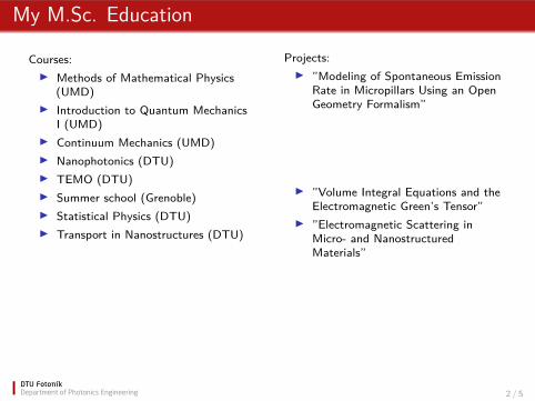
My M.Sc. Education
Courses:I Methods of Mathematical Physics
(UMD)I Introduction to Quantum Mechanics
I (UMD)I Continuum Mechanics (UMD)I Nanophotonics (DTU)I TEMO (DTU)I Summer school (Grenoble)I Statistical Physics (DTU)I Transport in Nanostructures (DTU)
Special courses and M.Sc. project:Chance to do research andpossibly publish an article.
Projects:I ”Modeling of Spontaneous Emission
Rate in Micropillars Using an OpenGeometry Formalism”
Modeling of cavities using the analytic modal methodand an open geometry formalism
Jakob Rosenkrantz de Lasson,† Thomas Christensen,† Jesper Mørk, and Niels Gregersen*
DTU Fotonik, Department of Photonics Engineering, Technical University of Denmark, Ørsteds Plads,Building 343, DK-2800 Kongens Lyngby, Denmark
*Corresponding author: [email protected]
Received September 27, 2011; revised March 12, 2012; accepted March 12, 2012;posted March 15, 2012 (Doc. ID 155363); published June 6, 2012
We present an eigenmode expansion technique for calculating the properties of a dipole emitter inside a micro-pillar. We consider a solution domain of infinite extent, implying no outer boundary conditions for the electricfield, and expand the field on analytic eigenmodes. In contrast to finite-sized simulation domains, this avoids theissue of parasitic reflections from artificial boundaries. We compute the Purcell factor in a two-dimensionalmicropillar and explore two discretization techniques for the continuous radiation modes. Specifically, an equi-distant and a nonequidistant discretization are employed, and while both converge, only the nonequidistant dis-cretization exhibits uniform convergence. These results demonstrate that the method leads to more accurateresults than existing simulation techniques and constitutes a promising basis for further work. © 2012 OpticalSociety of America
OCIS codes: 000.3860, 050.1755, 230.5750, 230.7370, 290.0290.
1. INTRODUCTIONQuantum emitters embedded in optical microcavities, such asphotonic crystals and micropillars, constitute an importantplatform for exploring a range of interesting physical phenom-ena as well as realizing quantum information devices. Thisincludes a broad range of interesting features, includingenhanced light–matter interactions, quantum entanglement,and single-photon emission [1]. The latter is intimately relatedto the Purcell effect that describes the enhancement or inhibi-tion of the spontaneous emission rate (SER) of an emitterwhen positioned inside an optical cavity [2]. Enhancementof the SER is vital in the development of efficient and reliablesingle-photon sources in the scope of quantum informationtechnology [3].
To obtain the desired functionality in such devices, ac-curate numerical modeling of the electromagnetic field is cru-cial. Numerical methods based on spatial discretization suchas finite-difference time-domain (FDTD) [4] and the finite ele-ment method (FEM) [5] are popular; however, the necessity ofdiscretizing the entire computational domain leads to hugememory requirements for realistic device geometries. On theother hand, modal methods such as the Fourier modal method[6] and eigenmode expansion technique (EET) [7] are lessmemory demanding, and in addition the approaches them-selves provide a better insight into governing physicalmechanisms of interest. In this article, we formulate and de-monstrate the application of the EET to a geometry withoutouter boundary conditions, the so-called open geometry thatis commonly encountered in optics.
In modal methods, or rigorous coupled-wave analysis, theelectromagnetic fields are expanded on a complete and ortho-normal set of basis functions. The set of basis functions can bechosen as the set of eigenmodes supported by the optical en-vironment under consideration, giving rise to the EET. These
eigenmodes can be determined using Fourier analysis or bydirect analytic determination of the eigenmodes. In a homo-geneous medium, the eigenmodes are indeed plane waves,but in more advanced structures, such as the micropillar tobe considered in this article, the complete set of eigenmodesincludes a finite number of guided modes and a continuum ofradiation modes.
A common issue for most of the suggested simulation tech-niques is that practical implementation enforces a finite-sizedsolution domain. In its simplest form, this implies the con-straint that the field must vanish at the boundaries of thesolution domain, which inevitably produces parasitic reflec-tions at these metal-like boundaries [8]. As a means to reducethese effects, absorbing boundaries, the so-called perfectlymatched layers (PMLs), were introduced [9]. The use of ana-lytic eigenmodes in combination with PML was investigatedby Bienstman and Baets [7,8], and numerically stable resultsusing this technique were demonstrated [10]. However, theuse of PMLs requires a set of parameters to be determinedthat define the boundary region, and convergence of the elec-tric field upon adjustment of these parameters, toward that ofan open geometry, is not guaranteed [11]. Thus, even PMLdoes not fully eliminate the parasitic perturbations of thefields [12], and this inherent deficiency of finite-sized simula-tion domains motivates the introduction of an open geometryof infinite extent.
The open geometry has been treated by expansion of theeigenmodes on a Fourier–Bessel basis [13]. On the other hand,expansions on analytical eigenmodes are applied in [14],where an open geometry with radiation from a waveguide intofree space is treated. There, an integral equation for the fieldat the interface between the waveguide and free space isderived and solved by a perturbative approach. First- andsecond-order solutions are presented, but the approximatesolution procedure in practice limits the index contrasts that
Rosenkrantz de Lasson et al. Vol. 29, No. 7 / July 2012 / J. Opt. Soc. Am. A 1237
1084-7529/12/071237-10$15.00/0 © 2012 Optical Society of America
I ”Volume Integral Equations and theElectromagnetic Green’s Tensor”
I ”Electromagnetic Scattering inMicro- and NanostructuredMaterials”
Downloaded 22 Oct 2012 to 192.38.90.11. Redistribution subject to AIP license or copyright; see http://proceedings.aip.org/about/rights_permissions
Three-dimensional integral equation approach to lightscattering, extinction cross sections, local density
of states, and quasi-normal modes
Jakob Rosenkrantz de Lasson,* Jesper Mørk, and Philip Trøst Kristensen
DTU Fotonik, Department of Photonics Engineering, Technical University of Denmark, Ørsteds Plads, Building 343,Kongens Lyngby DK-2800, Denmark
*Corresponding author: [email protected]
Received March 12, 2013; revised April 23, 2013; accepted April 24, 2013;posted May 21, 2013 (Doc. ID 186855); published June 27, 2013
We present a numerical formalism for solving the Lippmann–Schwinger equation for the electric field in threedimensions. The formalismmay be applied to scatterers of different shapes and embedded in different backgroundmedia, and we develop it in detail for the specific case of spherical scatterers in a homogeneous backgroundmedium. In addition, we show how several physically important quantities may readily be calculated withthe formalism. These quantities include the extinction cross section, the total Green’s tensor, the projected localdensity of states, and the Purcell factor as well as the quasi-normal modes of leaky resonators with the associatedresonance frequencies and quality factors. We demonstrate the calculations for the well-known plasmonic dimerconsisting of two silver nanoparticles and thus illustrate the versatility of the formalism for use in modeling ofadvanced nanophotonic devices. © 2013 Optical Society of America
OCIS codes: (000.3860) Mathematical methods in physics; (050.1755) Computational electromagneticmethods; (240.6680) Surface plasmons; (290.4210) Multiple scattering.http://dx.doi.org/10.1364/JOSAB.30.001996
1. INTRODUCTIONRealization of optical devices based on optical micro ornanostructures such as photonic crystals [1–3] or plasmonicnanoparticles [4–6] rely on a prolific interplay betweenadvanced fabrication techniques and accurate numericalmethods. The latter paves the way for the design of advancedoptical functionalities as well as systematic studies and in-depth understanding of the physical mechanisms at play.Additionally, numerical modeling serves as an indispensabletool in the interpretation of experimental results, and thestudy and development of numerical modeling methods there-fore remain an important and integral part of modern nano-photonics research. Propagation of light, in the form ofelectromagnetic fields, is governed by Maxwell’s equations,and in spite of being known for more than a century, theseequations remain very difficult to solve and display richbehavior. Analytical solutions are available only for a limitednumber of geometries, and numerical solvers are thus indis-pensable in the design of practical devices. Each numericalscheme has advantages and limitations, as analyzed, forexample, with photonic-crystal-based vertical-cavity surface-emitting lasers as benchmark structures using four differentmethods in [7]. The most prominent advantages of the integralequation approach that we present in this paper are versatilityin the form of easy access to figures of merit and high accu-racy with a built-in error measure.
The most popular numerical methods in the field ofnanophotonics are the finite-difference time-domain (FDTD)method [8] and the finite element method (FEM) [9], whichare both based on spatial discretization ofMaxwell’s equations.FDTD uses a rectangular grid and a simple time-stepping
procedure to evolve the fields in time,whereasFEMuses anon-uniform triangular meshing, which can more easily adapt tocurved surfaces, and is most often used for frequency-domainproblems. As a powerful hybrid approach, discontinuousGalerkin methods use a variant of FEM based on nonoverlap-ping basis functions, leading to improved performance in time-domain calculations [10]. Thesemethods can easily be adaptedto treat arbitrary structures, but the necessity to discretize theentire spacemay in practice lead to large requirements in termsof memory and computational power, in particular for three-dimensional (3D) problems. Alternatives includemodal expan-sion techniques such as the Fourier modal method [11] and theRayleigh multipole method [12], in which the fields are ex-panded on a chosen set of basis functions, and the electromag-netic boundary conditions (BCs) are satisfied to determine theexpansion coefficients. In FDTD, FEM, and modal expansiontechniques the need to minimize parasitic reflections from thecalculation domain boundaries usually entails the introductionof perfectlymatched layers (PMLs) [13]. Another class ofmeth-ods is based on surfaceor volume integrals [14]. One advantageof this procedure is that only bounded parts of space need to bediscretized, which prompts faster computations. Typical ap-proaches employ expansions of the fields on orthonormal setsof basis functions, and the integral equations are converted intosystems of linear equations for the expansion coefficients. Apopular choice of basis functions is the so-called pulse basisfunctions [15] that form the foundation of the discrete dipoleapproximation [16]. The simplicity of these piecewise-constantbasis functions allows a simple treatment of arbitrary geom-etries, but their simplicity in turn leads to very largesystems of equations. More severely, the pulse basis functions
1996 J. Opt. Soc. Am. B / Vol. 30, No. 7 / July 2013 de Lasson et al.
0740-3224/13/071996-12$15.00/0 © 2013 Optical Society of America
2 / 5

My Teaching Assistant Jobs
Courses:I Advanced Engineering Mathematics
1 (01005)I Introduction to Numerical
Algorithms (02601)I Introductory Programming with
Matlab (02631)I Partial Differential Equations –
Applied Mathematics (01246)I Thermodynamics and Statistical
Physics (10034)I Nanophotonics (34051)
Projects:I ”Semiconductor Quantum Dots”I ”Single-Photon Sources for
Quantum Information Processing”I ”Optical Simulations of Structured
Materials”
Teaching assistant jobs: Optimalway of reviewing courses andunderstanding curricula evenbetter.
And to earn money ¨̂
3 / 5

My Teaching Assistant Jobs
Courses:I Advanced Engineering Mathematics
1 (01005)I Introduction to Numerical
Algorithms (02601)I Introductory Programming with
Matlab (02631)I Partial Differential Equations –
Applied Mathematics (01246)I Thermodynamics and Statistical
Physics (10034)I Nanophotonics (34051)
Projects:I ”Semiconductor Quantum Dots”I ”Single-Photon Sources for
Quantum Information Processing”I ”Optical Simulations of Structured
Materials”
Teaching assistant jobs: Optimalway of reviewing courses andunderstanding curricula evenbetter.And to earn money ¨̂
3 / 5

What Does a Physicist Do?
Physicists develop mathematical models to predict and analyzecomplex phenomena.
And understand the limitations of the models.
4 / 5

What Does a Physicist Do?
Physicists develop mathematical models to predict and analyzecomplex phenomena.
And understand the limitations of the models.
4 / 5

What Does a Physicist Do?
Physicists develop mathematical models to predict and analyzecomplex phenomena.
And understand the limitations of the models.
4 / 5

What Does a Physicist Do?
Physicists develop mathematical models to predict and analyzecomplex phenomena. And understand the limitations of the models.
4 / 5

More Information
I Visit my homepage at www.jakobrdl.dk
I Visit my blog at www.ing.dk/blogs/dtu-indefra
I Visit www.fotonik.dtu.dk/nanotheory
I Send me an e-mail at [email protected]
...Thank you for your attention! Any questions?
5 / 5

More Information
I Visit my homepage at www.jakobrdl.dk
I Visit my blog at www.ing.dk/blogs/dtu-indefra
I Visit www.fotonik.dtu.dk/nanotheory
I Send me an e-mail at [email protected]
...Thank you for your attention! Any questions?
5 / 5

More Information
I Visit my homepage at www.jakobrdl.dk
I Visit my blog at www.ing.dk/blogs/dtu-indefra
I Visit www.fotonik.dtu.dk/nanotheory
I Send me an e-mail at [email protected]
...Thank you for your attention! Any questions?
5 / 5
More Information
I Visit my homepage at www.jakobrdl.dk
I Visit my blog at www.ing.dk/blogs/dtu-indefra
I Visit www.fotonik.dtu.dk/nanotheory
I Send me an e-mail at [email protected]
...Thank you for your attention! Any questions?
5 / 5

More Information
I Visit my homepage at www.jakobrdl.dk
I Visit my blog at www.ing.dk/blogs/dtu-indefra
I Visit www.fotonik.dtu.dk/nanotheory
I Send me an e-mail at [email protected]
...Thank you for your attention! Any questions?5 / 5