photonic based radar: characterization of 1x4 mach ... · radar systems 20 2.1. classification of...
TRANSCRIPT

i
Photonic based Radar: Characterization of 1x4 Mach-
Zehnder Demultiplexer
Umar Shahzad
Supervised by: Dr. Antonella Bogoni
Master in Computer Science and Networking

ii

iii
Acknowledgement
First and foremost, my utmost gratitude and deep appreciation goes to my supervisor,
Prof. Antonella Bogoni; and Filippo Scotti for their kindness, constant endeavour, guidance
and the numerous moments of attention they devoted throughout this work. I would like to
thank my supervisor for proposing the idea for this work and introducing me to the world of
Digital Photonics.
I would also like to thank Scuola Superiore Sant’anna TeCIP for providing me a
complete friendly research environment to accomplish this work.
Special thanks go to my family members for their unconditional support on this
endeavour of mine. At the end, I would like to acknowledge the financial, academic and
technical support of the University of Pisa and want to thank the Master Board for providing
me such opportunity.
iv
Abstract
This work is based on a research activity which aims to implement an optical
transceiver for a photonic-assisted fully–digital radar system based on optic miniaturized
optical devices both for the optical generation of the radiofrequency (RF) signal and for the
optical sampling of the received RF signal. The work is more focused on one very critical
block of receiver which is used to parallelize optical samples. Parallelization will result in
samples which will be lower in repetition rate so that we can use commercial available ADCs
for further processing. This block needs a custom design to meet all the system specifications.
In order to parallelize the samples a 1x4 switching matrix (demux) based on Mach Zehnder
(MZ) interferometer has been proposed. The demux technique is Optical Time Division
Demultiplexing. In order to operate this demux according to the requirements the
characterization of device is needed. We need to find different stable control points (coupler
bias and MZ bias) of demux to get output samples with high extinction ratio. A series of
experiments have been performed to evaluate the matrix performance, issues and sensitivity.
The evaluated results along with the whole scheme have been discussed in this document.

v

vi
Contents
1. INTRODUCTION 1
1.1. Introduction to Thesis 1
1.2. All Optical Signal Processing 3
1.2.1. Why Optical Processing over Electronics with some background 3
1.2.2. Some Developments 7
1.2.3. Limitations 12
1.3. Basics of Radar Principle 13
1.3.1. A Short History 14
1.3.2. Radar Basic Operational Principle 16
2. Radar Systems 20
2.1. Classification of Radar Systems 20
2.1.1. Depending on Technologies 20
2.1.1.1. Continuous Wave (CW) Radar 22
2.1.1.2. Frequency Modulated CW (FMCW) Radar 25
2.1.1.3. Bistatic Radar Set 29
2.1.1.4. Moving Target Indication (MTI) Radar 30
2.1.1.5. Pulse Doppler Radar 34
2.1.1.6. Pulse Compression in Radar 34
2.1.2. Depending on Design 36
2.1.2.1. Air-Defence Radars 36
2.1.2.2. Air Traffic Control (ATC)-Radars 37
2.2. Coherent and Non-Coherent Processing in Radars 39

vii
2.3. Radar Devices 40
2.3.1. Transmitter 40
2.3.1.1. Pseudo-coherent or Non-coherent Radar 41
2.3.1.2. Coherent Radar 45
2.3.2. Radar receiver 48
2.3.2.1. Super-heterodyne Receiver 48
2.4. Some limitations 51
3. Photonic based Radar: Characterization of 1x4 Mach-Zehnder Demux 52
3.1. Overall Scenario 52
3.1.1. Radio Frequency (RF) generation 52
3.1.2. Radar Receiver 56
3.1.2.1. Photonic Sampled and electronically Quantized ADCs 59
3.2. Characterization of 1x4 Mach-Zehnder Demultiplexer (demux) 62
3.2.1. Technological aspects 63
3.2.2. Mach Zehnder as Switch 65
3.2.3. Matching and Biasing network 66
3.2.4. Coupler Bias Voltage (Vbias coup) 68
3.2.5. Critical Observations 75
4. Conclusion 77
4.1. Current Status of Experiments 77
4.1.1. Driving Signal amplification and tuning 78
4.1.2. Experiment Results 80
5. References 82

viii


1
1. Introduction
1.1. Introduction to Thesis
In modern radar system in order to meet the requirements of high resolution,
sensitivity and flexibility the limitations in current electronic systems have to be overcome.
Coherent radar systems detect moving objects with excellent discrimination from weather
and background clutter, by extracting information from the phase of the echoes [1]. In order
to meet the required performance, the phase noise of the radar signal must be reduced as
much as possible. The spectral purity of the RF signals generated by electronic architectures
is mainly limited by the noisy frequency multiplication that worsens the signal quality as the
required frequency increases. The first requirement is to generate an RF signal which should
be phase coherent and able to achieve very high frequencies. The technologies which can
provide a significant benefits in terms of phase coherence, fast processing and high frequency
generation can rule the future radar world.
The second requirement is the efficient processing of the received signal along with
the deduction of those conventional electronic processes that lead to noise and distortion. The
conventional electronic radar receiver architecture also adds phase noise by frequency
multiplication, down-conversion; to shift the original frequency to an intermediate value
where the electrical analog-to-digital converters (ADCs) can be exploited. This element is the
main reason of distortions and phase noise. As far as ADCs are concerned, the ability to
implement flexible and high resolution digital-receiver architectures is often limited by the
performance of the ADC component. For example, electronic ADCs with sampling rates > 1
GS/s (giga-sample per second) are presently limited to resolutions of less than 7 effective bits

2
[44-dB signal-to-noise ratio (SNR)] [2] and ADCs having 12 effective bits (74-dB SNR) have
a maximum sampling rate of 65 MS/s (mega-sample per second).
In order to overcome the problems in current radar systems photonic solution proves
to be an alternative. The generation of RF signals in photonics allow the development of a
radar transmitter with high phase coherence, and ultra-high microwave frequency. As far as
receivers are concerned, radar systems could benefit significantly from high-resolution (12
bits) ADCs having mutli-gigahertz of instantaneous bandwidth. The flexibility of the
receivers in these systems can be augmented by pushing the ADC closer to the antenna and
performing more of the receiver functions in the digital domain. Photonic solutions for ADC
can be used to sample the received RF signal in photonic domain, which result in high
sampling rate and high resolution. This way down-conversion process can be avoid.
This thesis work is based on a research activity which aims to implement an optical
transceiver for a photonic-assisted fully–digital radar system based on optic miniaturized
optical devices both for the optical generation of the radiofrequency (RF) signal and for the
optical sampling of the received RF signal. This thesis is focused on one very critical block of
receiver which is used to parallelize optical samples. Parallelization will result in samples
which will be lower in repetition rate so that we can use commercial available ADCs for
further processing. This block needs a custom design to meet all the system specifications. In
order to parallelize the samples a 1x4 switching matrix (demux) based on Mach Zehnder
(MZ) interferometer has been proposed. The demux technique is Optical Time Division
Demultiplexing. Electro-optic technology has been used in the design of the switching matrix
to reduce the cost. In order to operate this demux according to our requirement the
characterization of device is needed. We need to find different stable control points (coupler
bias and MZ bias) of demux to get output samples with high extinction ratio. I have
performed a number of experiments in the Lab to evaluate the matrix performance, issues and
sensitivity.
Rest of this chapter is focused on the importance of all optical processing, some
developments and limitations in this regards and finally basics of radar system.

3
1.2. All Optical Signal Processing 1.2.1. Why Optical Processing over Electronics Processing with some
background
The dielectric waveguide proposed by Kao and Hockham in 1966 for guiding
lightwaves have revolutionized the transmission of broadband signals and ultrahigh capacity
over ultra-long global telecommunication systems and networks. In the 1970s, the reduction
of the fiber losses over the visible and infrared spectral regions was extensively investigated.
Since then, the research, development, and commercialization of optical fiber communication
systems progressed with practical demonstrations of higher and higher bit rates and longer
and longer transmission distance. Significantly, the installation of optical fiber systems was
completed in 1978. Since then, fiber systems have been installed throughout the world and
interconnecting all continents of the globe with terrestrial and undersea systems.
The primary reason for such exciting research and development is that the frequency
of the lightwave is in the order of a few hundred terahertz and the low loss windows of glass
fiber are sufficiently wide so that several tens of terabits per second capacity of information
can be achieved over ultra-long distance, whereas the carrier frequencies of the microwave
and millimeter-wave are in the tens of gigahertz [3]. Indeed in the 1980s, the transmission
speed and distance were limited because of the ability of regeneration of information signals
in the optical or photonic domain. Data signals were received and recovered in the electronic
domain; then the lightwave sources for retransmission were modulated. The distance between
these regenerators was limited to 40 km for installed fiber transmission systems. Furthermore,
the dispersion-limited distance was longer than that of the attenuation-limited distance, and
no compensation of dispersion was required.
The distance without repeater could then be extended to another 20 km with the use of
coherent detection techniques in the mid-1980s; heterodyne and homodyne techniques were
extensively investigated. But applications of coherent processing restrict due to phase
estimation (local oscillator for mixing) at receiver and complexity [3]. The attenuation was
eventually overcome with the invention of the optical amplifiers in 1987 using Nd or Er
doping in silica fiber. Optical gain of 20–30 dB can be easily obtained. Hence, the only major
issue was the dispersion of lightwave signals in long-haul transmission. This leads to
extensive search for the compensation of dispersion. The simplest method can be the use of

4
dispersion compensating fibers inserted in each transmission span, hence the phase reversal
of the lightwave and compensation in the photonic domain. This is a form of photonic signal
processing [3].
This leads to the development of high and ultrahigh bit rate transmission system. The
bit rate has reached 10, 40, and 80 Gb/s per wavelength channels in the late 1990s. Presently,
the transmission systems of several wavelength channels each carrying 40 Gb/s are
practically proven and installed in a number of routes around the world. With the passage of
time the trend is moving forward to attain ultrafast speed but to process these fast signals in
electronics is no longer possible due to bandwidth limitation of electronics and thus signal
processors in the photonic domain are expected to play a major role in these fast systems.
All optical processing can also be beneficial over electronics in term of power
consumption. Energy efficiency is becoming one of the key factors in almost every aspect of
daily life. The energy efficiency in the internet has recently been a hot topic due to growth of
Internet Traffic, which is keep on growing. Figure 1.1 shows the trend of total IP data traffic
growth worldwide, which is an average of 32% annually, between 2010 and 2015, reaching
approximately 80 exabytes (80 million terabytes) per month by 2015 [4]. The increasing
popularity of mobile terminals, especially smartphones, is further spurring data traffic. By
allowing users to access data-rich content through the Internet almost anywhere and anytime,
smartphones are generating 10 to 20 times more data traffic than conventional mobile phones
[4]. Figure 1.2 shows the trend of business IP traffic growth which is escalating worldwide
and “cloud computing” playing a big role in this growth.
Figure 1.1.Cisco Systems, Inc. estimates that global IP traffic will reach approxi-

5
mately 80 exabytes per month by 2015.
Figure 1.2.Business IP traffic is expected to increase annually by an average of 22%
between 2010 and 2015, reaching approximately 10 exabytes (10 million terabytes)
per month by 2015
This explosive growth leads to the need of energy efficient high capacity systems. In
this scenario, all optical processing can be a big alternative because it has already been
proven that high speed and energy efficiency can be achieved from photons. From Figure 1.3
below it can be analysed, by keeping in mind the increasing growth of Internet Traffic, that
why is it so important to go towards energy efficiency in ICT.
Figure 1.3.A view of Power Consumption
In order to well establish a point, mentioned in above paragraphs, that all optical
processing can be an attractive alternative over electronics let us consider two examples from

6
current network scenario. The Figure 1.4 below shows the schematic of internet today
depicting the complex heterogeneity of internet. The user may run a variety of applications
across wireless, wireline, and optical technologies running many different protocols. Packets
intended to run same applications between peers may take different paths based on wireless,
wireline, and/or optical technologies. In this situation, unified networking platform with high
capacity (optical layer) will be a real advantage [5]. If Internet packets process completely in
optical domain, while passing through the landline network, then we will attain a high
capacity power efficient system. Here it is worth mention that Electro-Optic conversion is
also not energy efficient.
.Figure 1.4.Complex Heterogeneity of today Internet
Another scenario is the all-optical short-range photonic interconnection networks. The
main hindrance in the improvement of the present high performance computing systems is
the bottleneck of the chip-to-chip and chip-to-memory communication. The limits are the
high wiring density, the high power consumption and the limited throughput [6]. Photonic
interconnection networks can overcome the limitations of the electronic interconnection
networks by guaranteeing high bit rate communications, data format transparency and
electromagnetic field immunity. Moreover they can reduce the wiring density and the power
consumption. In such networks photonic digital processing can be the most suitable paradigm
for simple and ultra-fast control and switching operations, since it reduces the packet latency
to the optical time-of-flight.

7
Beside power consumption and high capacity, below mentioned are some other
advantages of all optical processing.
High spectral and spatial coherence.
RF interference free.
Robustness to the cosmic radiations.
Low distortions in signal distribution.
1.2.2. Some Developments
The idea of all optical processing is to process the signals while they are still in the
photonic domain. The first proposal of the processing of signals in the optical/photonic
domain was coined by Wilner and van der Heuvel in 1976 [7] indicating that the low loss and
broadband transmittance of the single-mode optical fibers would be the most favourable
condition for processing of broadband signals in the optical/photonic domain. Since then,
several topical developments in this field, including integrated optic components, subsystems,
and transmission systems have been reported and contributed to optical communications.
Almost all traditional functions in electronic signal processing have been realized in the
optical/photonic domain.
In order to apply photonic processing (digital) for the controlling of the network data
plane, complex functions must be available. Recent developments in photonic digital
processing have been very well summarized in [8]. Below a brief description is mentioned.
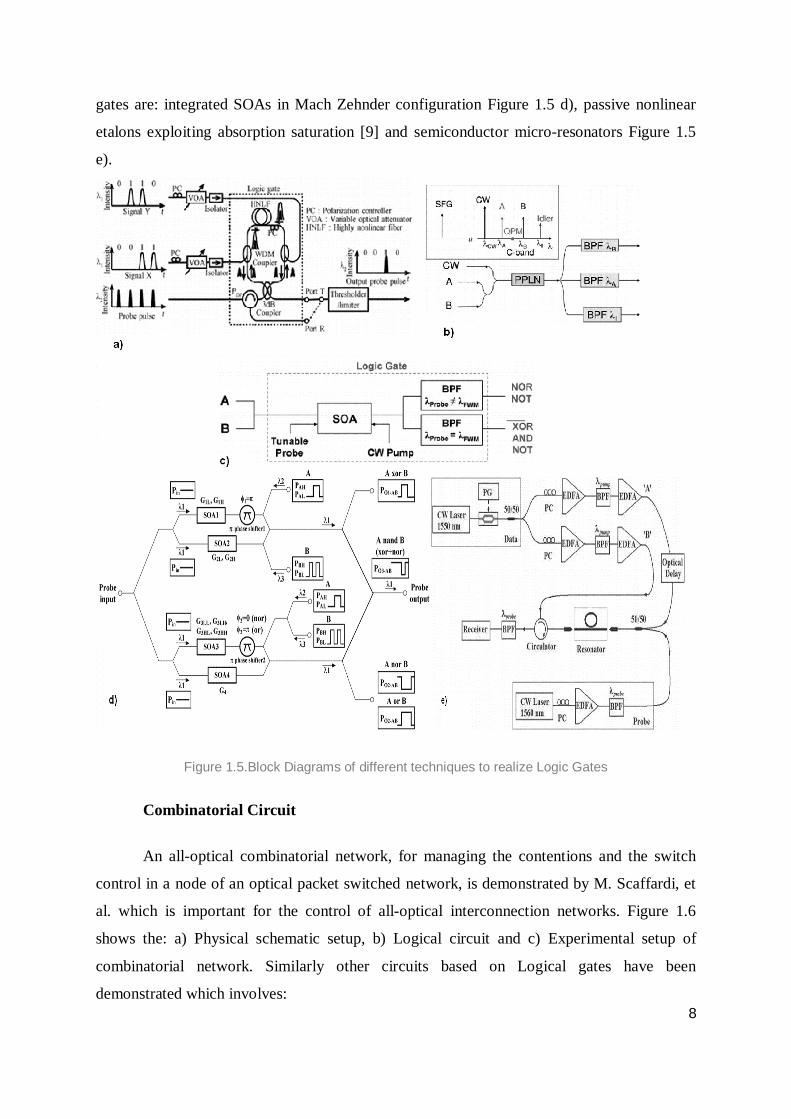
Logic Gates
Elementary logic gates as AND, NOR, NAND, NOT has been demonstrated with
fibre, waveguide and semiconductor-based solutions. A fibre-based scheme exploits Cross
Phase Modulation (XPM) in nonlinear optical loop mirrors structures shown in Figure 1.5 a).
A combination of pump depletion and Sum Frequency and Difference Frequency Generation
(SFG-DFG) has been exploited in a single Periodically Poled Lithium Niobate (PPLN)
waveguide in shown in Figure 1.5 b) to obtain multiple basic logic operations. The logical
gates based on Semiconductor solutions exploit Semiconductor Optical Amplifiers (SOAs)
followed by optical filtering as shown in Figure 1.5 c). Some other variants of SOA based
8
gates are: integrated SOAs in Mach Zehnder configuration Figure 1.5 d), passive nonlinear
etalons exploiting absorption saturation [9] and semiconductor micro-resonators Figure 1.5
e).
Figure 1.5.Block Diagrams of different techniques to realize Logic Gates
Combinatorial Circuit
An all-optical combinatorial network, for managing the contentions and the switch
control in a node of an optical packet switched network, is demonstrated by M. Scaffardi, et
al. which is important for the control of all-optical interconnection networks. Figure 1.6
shows the: a) Physical schematic setup, b) Logical circuit and c) Experimental setup of
combinatorial network. Similarly other circuits based on Logical gates have been
demonstrated which involves:

9
All-optical circuits for the pattern matching, i.e. able to determine if two Boolean
numbers are equal or not. Pattern matching by a XOR gate implemented with a nonlinear
optical loop mirror, by combining AND and XOR gates in a single Semiconductor Optical
Amplifier-Mach Zhender Interferometer (SOA-MZI). The cascade of SOA-MZI structures in
order to have a single output pulse in case of matching.
An SOA-based all-optical circuit for the comparison of 1-bit binary numbers.
Finally an all optical subsystem able to discriminate if an N-bit (with N>1) pattern
representing a binary number is greater or lower than another one is also demonstrated.
Figure 1.6.Setup of all-optical combinatorial network
Calculating the addition of binary numbers is another important functionality to
perform packet header processing. A Time-To-Live (TTL) field represents the maximum
number of hops of a packet and it is decremented after each node. When the field value is
zero, the packet is discarded and in this way avoids loop formation. So, to implement this
functionality an all-optical processing circuit able to perform the decrementing of the binary
number in the TTL field requires. Applying the compliments of all optical full-adder, this
operation can be performed. Moreover there are also many other applications of full-adder

10
like resolving the Viterbi algorithm in the Maximum-Likelihood Sequence Estimation
(MLSE) etc. An all-optical implementation of full-adder is fast and can improve of circuits.
Up to now few works report on the implementation of all-optical full-adders.
A.J. Poustie, et al. in 1999 employed SOA in a terabit optical asymmetric
demultiplexer configuration. The reported operation speed is below 1 Gb/s.
A faster full-adder based on SOAs is reported by J. H. Kim, et al. in 2003, but in that
scheme the output sum depends directly on the input carry; moreover performances in terms
of bit error-rate and eye opening are not reported.
In the SOA-based solution presented by M. Scaffardi, et al. in 2008 the sum and the
output carry do not depend directly on the input carry signal, thus potentially improving the
output signal quality when cascading multiple full-adders.
Finally a very fast half-adder and subtractor based on PPLN waveguide is reported in
in 2009 by A. Bogoni et al.
Flip-flops
Another important subsystem is the flip-flop. It generates a continuous optical signal
controlled by pulsed optical signals and allows the control of optical switches. Flip-flops are
demonstrated with Erbium-doped fibres Figure 1.7, and with integrated solutions.
Figure 1.7. Flip-flop based on Erbium-doped fibres
Some other Interesting solutions are based on coupled laser diodes, nonlinear polarization
switches, and coupled Mach-Zehnder interferometers. However the solution based on

11
coupled ring lasers is demonstrated by A. Malacarne, et al. in 2008, presents some advantages
as high contrast ratio, symmetric operations for set and reset and large input wavelength
range. The slow falling and rising edges of the flip-flop output signal is one of the most
critical aspects. Photonic processing on the flip-flop outputs can contribute to reduce the
falling and rising edge issues.
Switches and Add/drop modules
Other important basic elements for next generation optical networks are all-optical
switches and add/drop modules with Pico-second characteristic times, able to forward optical
packet without bit loss or to select single tributary channels from Optical Time Division
Multiplexing (OTDM) frames at very high bit rate (100 Gb/s and beyond). Highly nonlinear
fiber, nonlinear waveguide or SOA have been used for implementing ultra-fast switching
operation. Moreover new very promising silicon-based devices have been developed with
advantages in terms of cost, power consumption and CMOS compatibility by C.A. Barrios in
2004.
Photonic ADC and DAC
Photonic digital processing requires Analog-to-Digital and Digital-to-Analog
Converters (ADCs and DACs). Electronic A/D conversion is demonstrated up to 40
Gsamples/s with a 3-bit coding by W. Cheng, et al. in 2004. Nevertheless electronic A/D
conversion is mainly limited by the ambiguity of the comparators and jitter of the sampling
window [10]. The use of hybrid techniques employing an optical signal as sampling signal
improves the performances. In 2007 Wangzhe Li, et al. used polarization differential
interference and phase modulation to realize all-optical ADC, Figure 1.8 shows the schematic
and experimental setup of the technique. Optical sampling with amplitude modulators and
time and wavelength-interleaved pulses is demonstrated in [11]. In the last two mentioned
techniques the quantization and coding are exploited in the electronic domain. Likewise
different hybrid and all-optical techniques for ADC have been demonstrated over the time by
utilizing photonic processing i.e. Kerr-effect, nonlinear optical loop mirror (NOLM), self-
phase modulation (SPM), and cross gain modulation (XGM) in SOAs etc. SOAs based
approach enables analog-to-digital conversion with low optical power requirements with
respect to the fiber-based implementations and allows integrated solutions. Optical DAC is

12
appealing for its possible application in pattern recognition, and arbitrary waveform
generation for radar and display applications. S. Oda, and A. Maruta in 2006 and C. Porzi, et
al. in 2009 presented some of the DAC approaches.
Figure 1.8.All-Optical ADC based on polarization differential interference
and phase modulation
In conclusion, the possibility of using single basic building gates for implementing all
more complex logic functions seems to be the most practical approach. Nevertheless the
photonic digital processing is effective and attractive if it can be realised with integrated
solutions. SOAs have shown to be attractive because of their compactness, stability, low
switching energy and low latency. Therefore SOA based hybrid integrated solutions represent
a first step towards the integration of such complex functionalities. On the other hand the
development of silicon photonics makes photonic processing more attractive for green and
low cost solutions and it represents a turning point in the next generation optical network
evolution. Of course technology development and cross-fertilization between technology and
system fields are key issues to make photonic digital processing the basis of the future
networks.
1.2.3. Limitations
Photonic processing is in its early stage and the realisation of complete all-optical
computing system is still far, no all kind of digital photonic processors have been
implemented till now. Already proposed prototype performances are still not comparable
with electrical digital processors. Photonic technologies are not mature enough to take the

13
place of electronics, which is well matured. Technologies issues are at the moment the main
limitation to the photonic digital processing development. Lacking of efficient all-optical
memories is a big hurdle in all-optical systems currently. Electrons have an advantage over
photons that they can store information. Some proposal has been presented to realize buffer
functionality but again far from implementation phase. Integration is another issue currently
in all-optical processing although some prototype has been proposed. If experimental setups
of above mentioned developments have been followed then one can easily put integration
under limitation of all-optical processing. Emerging novel optical technologies, such as
nanostructured photonic crystal devices, high-contrast silicon optics, or semiconductor
quantum dots, promise to decrease the size and power dissipation of photonic integrated
circuits to the point where highly integrated systems on a chip can be envisioned. These
technologies are far from being mature, and much research has still to be done.
1.3. Basics of Radar Principle
Radar (Radio Detection And Ranging) is an electromagnetic system for object-
detection and to determine the range, altitude, direction, or speed of objects. It can be used to
detect aircraft, ships, spacecraft, guided missiles, motor vehicles, weather formations, and
terrain. The radar dish or antenna transmits pulses of radio waves or microwaves, a pulse-
modulated sine wave for example, which bounce off any object in their path. The object
returns a tiny part of the wave's energy to a dish or antenna which is usually located at the
same site as the transmitter. Radar is used to extend the capability of one’s senses for
observing the environment, especially the sense of vision. Radar can be designed to see
through those conditions impervious to normal human vision, such as darkness, haze, fog,
rain and snow. In addition, the most important attribute of radar is of being able to measure
the distance or range to the object, which is not possible with human vision.

14
Figure 1.9.Radar basic principal
1.3.1. A Short History
Neither a single nation nor a single person can say that the discovery and development
of radar technology was his (or its) own invention. One must see the knowledge about
“Radar” than an accumulation of many developments and improvements, in which any
scientists from several nations took part in parallel.
As early as 1865, The Scottish physicist James Clerk Maxwell presents his Theory of
the Electromagnetic Field (description of the electromagnetic waves and their propagation)
He demonstrated that electric and magnetic fields travel through space in the form of waves,
and at the constant speed of light. In 1886, Heinrich Hertz showed that radio waves could be
reflected from solid objects. In 1895 Alexander Popov, a physics instructor at the Imperial
Russian Navy school in Kronstadt, developed an apparatus using a coherer tube for detecting
distant lightning strikes. The next year, he added a spark-gap transmitter. In 1897, while
testing this in communicating between two ships in the Baltic Sea, he took note of
an interference beat caused by the passage of a third vessel. In his report, Popov wrote that
this phenomenon might be used for detecting objects, but he did nothing more with this
observation.
The German Christian Huelsmeyer was the first to use radio waves to detect "the
presence of distant metallic objects". In 1904 he demonstrated the feasibility of detecting a
ship in dense fog but not its distance. He obtained a patent for his detection device in April
1904 and later a patent for a related amendment for determining the distance to the ship. He

15
also got a British patent on September 23, 1904 for the first full radar application, which he
called telemobiloscope. In August 1917 Nikola Tesla outlined a concept for primitive radar
units. He stated, "...by their (standing electromagnetic waves) use we may produce at will,
from a sending station, an electrical effect in any particular region of the globe; (with which)
we may determine the relative position or course of a moving object, such as a vessel at sea,
the distance traversed by the same, or its speed."
In 1922 A. Hoyt Taylor and Leo C. Young, researchers working with the U.S. Navy,
discovered that when radio waves were broadcast at 60 MHz it was possible to determine the
range and bearing of nearby ships in the Potomac River. Despite Taylor's suggestion that this
method could be used in low visibility, serious investigation began eight years later after the
discovery that radar could be used to track airplanes.
Before the Second World War, researchers in France, Germany, Italy, Japan,
the Netherlands, the Soviet Union, the United Kingdom, and the United States, independently
and in great secrecy, developed technologies that led to the modern version of
radar. Australia, Canada, New Zealand, and South Africa followed pre-war Great Britain,
and Hungary had similar developments during the war.
In 1934 the Frenchman Émile Girardeau stated he was building an obstacle-
locating radio apparatus "conceived according to the principles stated by Tesla" and obtained
a patent for a working system, a part of which was installed on the Normandie liner in 1935.
During the same year, the Soviet military engineer P.K.Oschepkov, in collaboration
with Leningrad Electro-physical Institute, produced an experimental apparatus, RAPID,
capable of detecting an aircraft within 3 km of a receiver. The French and Soviet systems,
however, had continuous-wave operation and could not give the full performance that was
ultimately at the centre of modern radar.
Full radar evolved as a pulsed system, and the first such elementary apparatus was
demonstrated in December 1934 by American Robert M. Page, working at the Naval
Research Laboratory. The following year, the United States Army successfully tested
primitive surface to surface radar to aim coastal battery search lights at night. This was
followed by a pulsed system demonstrated in May 1935 by Rudolf Kühnhold and the
firm GEMA in Germany and then one in June 1935 by an Air Ministry team led by Robert

16
A. Watson Watt in Great Britain. Later, in 1943, Page greatly improved radar with
the mono-pulse technique that was used for many years in most radar applications.
The British were the first to fully exploit radar as a defence against aircraft attack.
This was spurred on by fears that the Germans were developing death rays. The Air Ministry
asked British scientists in 1934 to investigate the possibility of propagating electromagnetic
energy and the likely effect. Following a study, they concluded that a death ray was
impractical but that detection of aircraft appeared feasible. Robert Watson Watt's team
demonstrated to his superiors the capabilities of a working prototype and then patented the
device. It served as the basis for the Chain Home network of radars to defend Great Britain.
In April 1940, Popular Science showed an example of a radar unit using the Watson-Watt
patent in an article on air defence, but not knowing that the U.S. Army and U.S. Navy were
working on radars with the same principle, stated under the illustration, "This is not U.S.
Army equipment." Also, in late 1941 Popular Mechanics had an article in which a U.S.
scientist conjectured what he believed the British early warning system on the English east
coast most likely looked like and was very close to what it actually was and how it worked in
principle.
The war precipitated research to find better resolution, more portability, and more
features for radar, including complementary navigation systems like Oboe used by the RAF's
Pathfinder.
1.3.2. Radar Basic Operational Principle
The basic principle of operation [12] of primary radar is simple to understand.
However, the theory can be quite complex. Some laws of nature have a greater importance
here. Radar measurement of range, or distance, is made possible because of the properties of
radiated electromagnetic energy.
1. Reflection of electromagnetic waves: The electromagnetic waves are reflected if
they meet an electrically leading surface. If these reflected waves are received again at the
place of their origin, then that means an obstacle is in the propagation direction.
2. Electromagnetic energy travels through air at a constant speed, at approximately
the speed of light,

17
300,000 kilometres per second or
186,000 statute miles per second or
162,000 nautical miles per second.
This constant speed allows the determination of the distance between the reflecting objects
(airplanes, ships or cars) and the radar site by measuring the running time of the transmitted
pulses.
3. This energy normally travels through space in a straight line, and will vary only
slightly because of atmospheric and weather conditions. By using special radar antennas this
energy can be focused into a desired direction. Thus the direction (in azimuth and elevation)
of the reflecting objects can be measured.
These principles can basically be implemented in a radar system, and allow the
determination of the distance, the direction and the height of the reflecting object. (There will
be the effects of atmosphere and weather on the transmitted energy; however, for this
discussion on determining range and direction, these effects will be temporarily ignored.)
The below combination of figures show the operating principle of a primary radar set.
The radar antenna illuminates the target with a microwave signal, which is then reflected and
picked up by a receiving device. The electrical signal picked up by the receiving antenna is
called echo or return. The radar signal is generated by a powerful transmitter and received by
a highly sensitive receiver.
All targets produce a diffuse reflection i.e. it is reflected in a wide number of
directions. The reflected signal is also called scattering. Backscatter is the term given to
reflections in the opposite direction to the incident rays. Radar signals can be displayed on the
traditional plan position indicator (PPI) or other more advanced radar display systems. A PPI
has a rotating vector with the radar at the origin, which indicates the pointing direction of the
antenna and hence the bearing of targets.
Transmitter: The radar transmitter produces the short duration high-power RF pulses
of energy that are into space by the antenna.

18
Duplexer: The duplexer alternately switches the antenna between the transmitter and
receiver so that only one antenna need be used. This switching is necessary because the high-
power pulses of the transmitter would destroy the receiver if energy were allowed to enter the
receiver.
Receiver: The receivers amplify and demodulate the received RF-signals. The
receiver provides video signals on the output.
Radar Antenna: The Antenna transfers the transmitter energy to signals in space
with the required distribution and efficiency. This process is applied in an identical way on
reception.
Indicator: The indicator should present to the observer a continuous, easily
understandable, graphic picture of the relative position of radar targets. The radar screen (in
this case a PPI-scope) displays the echo signals in the form of bright spots called blips. The
longer the pulses were delayed by the runtime, the further away from the centre of this radar
scope they are displayed. The direction of the deflection on this screen is that in which the
antenna is currently pointing.

19
Figure 1.10.Step-by-step demonstration of basic processes involve in Radar

20
2. Radar Systems
In this chapter some details about Radar system is given. This discussion will
elaborate the type of processing involved in that system and will help to understand what the
limitations are in current electronic version of radar which can be handled in the optical
version.
2.1. Classification of Radar System Radar systems can be classified in term of Technologies and in term of Design. A
brief detail of different radars has been mentioned so that we can reach to the conclusion that
what has already been done, what else needed and which technology can be utilized to
enhance the performance of radars.
2.1.1. Depending on Technologies
By technologies, in this perspective, mean that what type of signal processing is
involved to realize radar to serve some purposes. Before going into the detail of different
radar technologies, it is worth to mention an effect which is not only important in radar but
also important in other fields like optics and acoustics. This effect is called as Doppler’s
Effect. In upcoming topic it will be seen that how much importance this effect possess in
radar systems.
The Doppler’s Effect:
The Doppler effect (or Doppler shift), named after Austrian physicist Christian
Doppler who proposed it in 1842, is the difference between the observed frequency and the
emitted frequency of a wave for an observer moving relative to the source of the waves. It is

21
commonly heard when a vehicle sounding a siren approaches, passes and recedes from an
observer. The received frequency is higher (compared to the emitted frequency) during the
approach, it is identical at the instant of passing by, and it is lower during the recession. This
variation of frequency also depends on the direction the wave source is moving with respect
to the observer; it is maximum when the source is moving directly toward or away from the
observer and diminishes with increasing angle between the direction of motion and the
direction of the waves, until when the source is moving at right angles to the observer, there
is no shift. The Figure 2.1 shows the change in the frequency with respect to observers and
source.
Figure 2.1.Frequency behaviour due to Doppler’s effect
Let’s try to represent this fact in mathematics with the perspective of radar. If R is the
distance from the radar to target, the total number of wavelengths λ contained in the two-way
path between the radar and the target is 2R/λ. The distance R and the wavelength λ are
assumed to be measured in the same units. Since one wavelength corresponds to an angular
excursion of 2π radians, the total angular excursion Φ made by the electromagnetic wave
during its transit to and from the target is 4πR/λ radians. If the target is in motion, R and the
phase Φ are continually changing. A change in Φ with respect to time is equal to a
frequency. This is the Doppler angular frequency ωd [13] given by
ωd = 2πfd = dΦ/dt = (4π/λ)(dR/dt) = 4πvr/λ

22
where fd = Doppler frequency shift
vr = relative velocity of target w.r.t radar
The Doppler frequency shift is
fd = 2vr/λ = 2vrf0/c (2.1)
where f0 = transmitted frequency
c = 3 × 10⁸ m/s
There are four ways of producing the Doppler’s effect. Radars may be coherent pulsed
(CP), pulse-doppler radar, continuous wave (CW), or frequency modulated (FM). The earliest
radar experiments were based on the continuous transmissions. The types of radar which
involve continuous transmission are CW (continuous wave) and FM-CW (frequency
modulated – continuous wave).
2.1.1.1. Continuous Wave (CW) Radar
The study of CW radar serves better to understand the nature and use of Doppler
information contained in the echo signal. The CW radar provides a measurement of relative
velocity which may be used to distinguish moving targets from stationary objects or clutter.
Clutter refers to radio frequency (RF) echoes returned from targets which are uninteresting to
the radar operators. In addition, this type of radar has many interesting applications, which
will be presented.
A simple CW radar is shown in the below block diagram, Figure 2.2. A continuous
(un-modulated) signal of frequency ‘f0’ has been generated by transmitter and radiated by
antenna. The portion of radiated energy, after intercepting from target, scattered in the
different direction and some of it scattered back in the direction of radar. The back scattered
signal is collected by the receiving antenna (in this case same as transmitted antenna). If the
target is in motion with some velocity , relative to the radar, the received signal will be
shifted in frequency from the transmitted frequency f0 by an amount “+” or “-” fd as
given by Eq. (2.1). The plus sign associated with the Doppler frequency applies if the
distance between target and radar is decreasing (closing target), that is, when the

23
received signal frequency is greater than the transmitted signal frequency. The minus
sign applies if the distance is increasing (receding target). The received echo signal at a
frequency f ± fd enters the radar via the antenna and is heterodyned in the detector
(mixer) with a portion of the transmitter signal f0 to produce a Doppler beat note of
frequency fd [13]. The sign of fd is lost in this process.
Figure 2.2.Block Diagram of CW radar
A single antenna serves the purpose of transmission and reception in the simple CW radar
described above. In principle, a single antenna may be employed since the necessary
isolation between the transmitted and the received signals is achieved via separation in
frequency as a result of the Doppler effect. In practice, it is not possible to eliminate
completely the transmitter leakage. However, transmitter leakage is not always undesirable.
A moderate amount of leakage entering the receiver along with the echo signal supplies
the reference necessary for the detection of the Doppler frequency shift. If a leakage
signal of sufficient magnitude were not present, a sample of the transmitted signal would
have to be deliberately introduced into the receiver (as shown in above figure) to provide the
necessary reference frequency.
The amount of isolation between transmitted and received signals depends on the
transmitter power and the accompanying transmitter noise as well as the sensitivity of the
receiver. Additional isolation requires in the CW long-range radar because of high
transmitted power and receiver sensitivity. Moreover, the amount of isolation in long-range
CW radar is more often determined by the noise that accompanies the transmitter leakage
signal rather than by any damage caused by high power. The largest isolations are obtained
with two antennas-one for transmission, the other for reception-physically separated from.one

24
another. The more directive the antenna beam and the greater the spacing between antennas,
the greater will be the isolation [13].
Intermediate-frequency receiver: The receiver of the simple CW radar of Figure 2.2 is in
some respects analogous to a super-heterodyne receiver. Receivers of this type are called
homodyne receivers, or super-heterodyne receivers with zero IF. The function of the local
oscillator is replaced by the leakage signal from the transmitter. Such a receiver is simpler
than one with a more conventional intermediate frequency since no IF amplifier or local
oscillator is required. However, the simpler receiver is not as sensitive because of increased
noise at the lower intermediate frequencies caused by flicker effect. Flicker-effect noise
occurs in semiconductor devices such as diode detectors and cathodes of vacuum tubes. The
noise power produced by the flicker effect varies with frequency. This is in contrast to shot
noise or thermal noise, which is independent of frequency. Thus, at the lower range of
frequencies (audio or video region), where the Doppler frequencies usually are found, the
detector of the CW receiver can introduce a considerable amount of flicker noise, resulting in
reduced receiver sensitivity. For short-range, low-power, applications this decrease in
sensitivity might be tolerated since it can be compensated by a modest increase in antenna
aperture and/or additional transmitter power. But for maximum efficiency with CW radar, the
reduction in sensitivity caused by the simple Doppler receiver with zero IF cannot be
tolerated.
The effects of flicker noise are overcome in the normal super-heterodyne receiver by
using an intermediate frequency high enough to render the flicker noise. Figure 2.3 below
shows a block diagram of the CW radar whose receiver operates with a nonzero IF. Separate
antennas are shown for transmission and reception instead of the usual local oscillator found
in the conventional super-heterodyne receiver, the local oscillator (or reference signal) is
derived in this receiver from a portion of the transmitted signal mixed with a locally
generated signal of frequency equal to that of the receiver IF. Since the output of the mixer
consists of two sidebands on either side of the carrier plus higher harmonics, a narrowband
filter selects one of the sidebands as the reference signal. The improvement in receiver
sensitivity with an intermediate-frequency super-heterodyne might be as much as 30 dB over
the simple receiver of Figure 2.3.

25
Figure 2.3.Block diagram of CW radar with nonzero IF receiver
One of the greatest shortcomings of the simple CW radar is its inability to obtain a
measurement of range which is related to the relatively narrow spectrum (bandwidth) of its
transmitted waveform. It lacks the timing mark necessary to allow the system to time
accurately the transmit and receive cycle and convert the measured round-trip-time
into range. This limitation can be overcome by modulating the CW carrier, as in the
frequency-modulated radar described next.
2.1.1.2. Frequency Modulated CW (FMCW) Radar
The spectrum of a CW transmission can be broadened by the application of
modulation, which can be amplitude, frequency, or phase. An example of an amplitude
modulation is the pulse radar. The narrower the pulse, the more accurate the measurement of
range and the broader the transmitted spectrum [13]. A widely used technique to broaden the
spectrum of CW radar is to frequency-modulate the carrier. The timing mark, for range
measurement, is the changing frequency. The transit time is proportional to the difference in
frequency between the echo signal and the transmitted signal.
A block diagram illustrating the principle of the FM-CW radar is shown in Figure 2.4
below. A portion of the transmitter signal acts as the reference signal required to produce the

26
beat frequency when heterodyned. It is introduced directly into the receiver via a cable or
other direct connection.
Figure 2.4, Block diagram of FM-CW radar
Ideally, the isolation between transmitting and receiving antennas is made sufficiently large
so as to reduce the transmitter leakage signal, which arrives at the receiver via the coupling
between antennas, to a negligible level. The beat frequency is amplified and limited to
remove any amplitude fluctuations. The frequency of the amplitude-limited beat note is
measured with a cycle-counting frequency meter calibrated in distance.
Range and Doppler measurement: Assume that the transmitter frequency increases linearly
with time, as shown by the solid line in Figure 2.5. If there is a reflecting object at a distance
R, an echo signal will return after a time T = 2R/c. The dashed line in the Figure 2.5
represents the echo signal. If the echo signal is heterodyned with a portion of the transmitter
signal in a nonlinear element such as a diode, a beat note fb will be produced. If there is no
Doppler frequency shift, the beat note (difference frequency) is a measure of the target's
range and fb = fr, where fr is the beat frequency due only to the target's range. If the rate of
change of the carrier frequency f0 the beat frequency is
fr = f0 T = 2R f0/c

27
Figure 2.5.Linear Frequency Modulation
In any practical CW radar, the frequency cannot be continually changed in one direction only.
Periodicity in the modulation is necessary, like the modulation can be in triangular, saw-
tooth, sinusoidal, or some other shape. If the frequency is modulated at a rate fm over a range
∆f the beat frequency is
fr = (2R /c)2fm ∆f = 4Rfm ∆f/c (2.2)
Thus the measurement of the beat frequency determines the range R.
As mentioned in the previous topic, simple CW radar can be used to measure target
speed through the Doppler shift. FM-CW radar also ends up being affected by the Doppler
shift, which creates an ambiguity. Suppose the FM-CW radar isn't moving and it's generating
a ramp of rising frequencies. If it transmits a particular frequency at a certain time, then when
it receives an echo after a specific delay time with the same frequency there is no ambiguity.
The round-trip time of the signal is just the measured delay, and the range is easy to calculate.
However, if the FM-CW radar is moving ahead, as it might be expected to if it's
installed in an aircraft and pointed forward to the ground, then the Doppler shift will drive up
the frequency of the return. If the return signal comes back with a particular frequency, it's
actually a Doppler-shifted return from a transmission at a lower frequency, and the range is
actually greater than would be expected from the delay time between transmission and
reception of the same frequency. Of course, if the FM-CW radar was moving backward the
return would be shifted down in frequency and the range would be shorter, but aircraft do not
fly backwards in normal operation.

28
The way around this is to generate the ramp of frequencies up and down in a
triangular fashion. To show how this works, let's assume again that the FM-CW radar is
stationary and compare the frequency-versus-time plot for transmit and receive, along with a
plot of the difference between the two:
Figure 2.6. (a) Triangular frequency modulation, (b) beat note of (a) for stationary FM-CW
radar
As the illustration in Figure 2.6 above shows, for a stationary FM-CW radar the return
signal tracks the transmit signal perfectly, returning with a fixed delay. Notice that at any
single time on the plot there is a constant difference between the transmit and receive
frequencies, except for the short window between the time the transmit signal changes
direction and receive signal follows.
Now let's put the FM-CW radar into forward motion and create the same plot. The
return from stationary target is rendered in light gray in below Figure 2.7 to provide a
reference.

29
Figure 2.7.Moving FM-CW radar
The Doppler shift creates a distinctive offset between the transmit signal and the
receive signal. This is because on the rising half of the ramp the transmit frequency is
increasing and the increased Doppler-shifted return signal is "catching up" with the changing
transmit signal, but on the falling half of the ramp the transmit signal is decreasing and the
increased Doppler-shifted receive signal is "lagging behind" the changing transmit signal.
This means the difference between the transmit and receive frequencies is small on
the rising half of the ramp, and large on the falling half of the ramp. FM-CW radar can use
this difference to determine both range and speed. Since the Doppler-shifted component is
subtracted on the rising half of the ramp and added on the falling half of the ramp, the range
is given by the average difference of the two cycles i.e. 1/2[fb (up) + fb (down)] = fr.
fb (up) = fr - fd
fb (down) = fr + fd
This average can be subtracted from the difference in the second half of the cycle to
give the Doppler-shifted velocity component, given as "fd" in the Figure 2.7. The FM-CW
radar principle is used in the aircraft radio altimeter to measure height above the surface of
the earth.
2.1.1.3. Bistatic Radar Set

30
Generally, the transmitter and receiver share a common antenna, which is called a
monostatic radar system. A bistatic radar consists of separately located (by a considerable
distance) transmitting and receiving sites as shown in Figure 2.8. Therefore, a monostatic
Doppler radar can be upgraded easily with a bistatic receiver system or (by use of the same
frequency) two monostatic radars are working like a bistatic radar. A bistatic radar makes use
of the forward scattering of the transmitted energy.
In case of a bistatic radar set there is a larger distance between the transmitting unit
and the receiving unit and usually a greater parallax. This means, a signal can also be
received when the geometry of the reflecting object reflects very little or no energy (stealth
technology) in the direction of the monostatic radar.
Figure 2.8.Bistatic Radar separate transmitter and receiver
In practice it is mainly used for weather radar. This system is also of some importance
in military applications. The so called “semi-active” missile control system, as used in the
missile unit “HAWK” is practically a bistatic radar.
By receiving the side lobes of the transmitting radars direct beam, the receiving sites
radar can be synchronized. If the main lobe is detected, an azimuth information can be
calculated also. A number of specialized bistatic systems are in use, for example, where
multiple receiving sites are used to correlate target position.
2.1.1.4. Moving Target Indication (MTI) Radar
The Doppler frequency shift produced by a moving target may be used in pulse radar
just as in the CW radar discussed above, to determine the relative velocity of a target or to
separate desired moving targets from undesired stationary objects (clutter). The use of

31
Doppler to separate small moving targets in the presence of large clutter has probably been of
far greater interest. MTI radar is pulse radar that utilizes the Doppler frequency shift to
discriminate moving targets from the fixed ones.
MTI is a necessity in high-quality air-surveillance radars that operate in the presence
of clutter. Its design is more challenging than that of simple pulse radar or simple CW radar.
In principle, the CW radar may be converted into a pulse radar as shown in the Figure 2.9 by
providing a power amplifier and a modulator to turn the amplifier on and off for the purpose
of generating pulses. In case of pulse radar as shown below a small portion of the CW
oscillator power that generates the transmitted pulses is diverted to the receiver to take the
place of the local oscillator. This CW signal acts as a replacement for the local oscillator as
well as coherent (will be explained later) reference needed to detect the Doppler frequency
shift.
Power Amplifier
Receiver Indicator
CW Oscillator ft
Pulse Modulator
f t
Reference Signal
fdft ± fd
Figure 2.9.MTI radar block diagram
If the CW oscillator voltage is represented as A1 sin 2πftt, where A1 is the amplitude
and ft the carrier frequency, the reference signal is
Vref = A2 sin 2πftt
And the Doppler-shifted echo signal voltage is

32
Vecho = A3 sin [2π(ft ± fd)t - 4πftR0/c]
where A2 = Amplitude of reference signal
A3 = Amplitude of signal received from target at range R0
fd = Doppler frequency shift
t = time, c = velocity of propagation
The reference signal and the target echo signal are heterodyned in the mixer stage of the
receiver. Only the low-frequency (difference-frequency) component from the mixer is of
interest and voltage is given by
Vdiff = A4 sin (2πfdt - 4πftR0/c) (2.3)
For stationary targets the Doppler frequency shift will be zero; hence Vdiff will not
vary with time and may take on any constant value from +A4 to –A4, including zero.
However, when the target is in motion relative to the radar, fd has a value other than zero and
the voltage corresponding to the difference frequency from the mixer Eq. (2.3) will be a
function of time [13].
The simple MTI radar shown in Figure 2.9 above is not the most typical. The block
diagram of more common MTI radar employing a power amplifier is shown in Figure 2.10
below and the difference is the way in which the reference signal is generated. The coherent
reference is supplied by an oscillator called the coho, as shown in the Figure, which stands
for coherent oscillator. The coho is a stable oscillator whose frequency is the same as the
intermediate frequency used in the receiver. In addition to providing the reference signal, the
output of the coho fc is also mixed with the local-oscillator frequency fl. The local oscillator
must also be a stable oscillator and is called stalo. The RF echo signal is heterodyned with the
stalo signal to produce the IF signal just as in the conventional super-heterodyned receiver.
The characteristic feature of coherent MTI radar is that the transmitted signal must be
coherent (in phase) with the reference signal in the receiver. This is accomplished in the radar
system by generating the transmitted signal from the coho reference signal. The function of
the stalo is to provide the necessary frequency translation from the IF to the transmitted (RF)
frequency. Although the phase of the stalo influences the phase of the transmitted signal, any

33
stalo phase shift is cancelled on reception because the stalo that generates the transmitted
signal also acts as the local oscillator in the receiver. The reference signal from the coho and
the IF echo signal are both fed into a mixer called the phase detector. The phase detector
differs from the normal amplitude detector since its output is proportional to the phase
difference between the two input signals.
Figure 2.10.Block diagram of more common MTI radar
The delay-line canceler acts as a filter to eliminate the d-c component of fixed targets and to
pass the a-c components of moving targets i-e to separate fixed targets from moving ones.
Simple MTI using analog technology is a straightforward idea, but it's not very
sophisticated; it results in a signal that is noisy and difficult to interpret. A more sophisticated
scheme is the "Ground Moving Target Indicator (GMTI)", discussed below.

34
One of the problems with MTI as described is that it won't work if the radar platform
is moving, since then the clutter returns will be very different from pulse to pulse and won't
cancel out.
A trick was developed that could be used to make a radar carried in an aircraft look
like it is standing still, at least from one pulse to the next. Suppose an aircraft has two radar
antennas in tandem and is taking radar observations to the side of the aircraft flight track. The
leading antenna emits a pulse, then advances forward and picks up the return. When the
trailing antenna reaches the position where the leading antenna was when it emitted its pulse,
the trailing antenna emits its own pulse, and then advances to pick the return in the same
position as did the leading antenna. This gives two pulses and returns obtained in the same
location, allowing a clutter canceler to be used to compare them to find moving targets.
2.1.1.5. Pulse Doppler Radar
Pulse radar that extracts the Doppler frequency shift for the purpose of detecting
moving targets in the presence of clutter is either MTI radar or a pulse Doppler radar. The
distinction between them is based on the fact that in a sampled measurement system like
pulse radar, ambiguities can arise in both the Doppler frequency (relative velocity) and the
range (time delay) measurements. Range ambiguities are avoided with a low sampling rate
(low pulse repetition frequency (PRF)), and Doppler frequency ambiguities are avoided with
a high sampling rate. However, in most radar applications the sampling rate, or PRF, cannot
be selected to avoid both types of measurement ambiguities. Therefore a compromise must be
made and the nature of the compromise generally determines whether the radar is called an
MTI or a pulse doppler. MTI usually refers to a radar in which the PRF is chosen low enough
to avoid ambiguities in range (no multiple-time-around echoes) but with the consequence that
the frequency measurement is ambiguous and results in blind speeds. Those relative target
velocities which result in zero MTI response are called blind speeds and it also one of the
limitations of MTI radar. The pulse doppler radar, on the other hand, has a high pulse
repetition frequency that avoids blind speeds, but it experiences ambiguities in range.
2.1.1.6. Pulse Compression in Radar
As mentioned in last section, there is a trade-off in determining pulse width. A short
pulse gives better range accuracy, but it also means less energy dumped out to sense a target.

35
Pulse Doppler makes the matter worse: interpreting the Doppler shift from a short pulse is
harder than interpreting the shift from a long pulse, and so a short pulse gives poorer velocity
resolution. A modern improvement in radar is known as "pulse compression" which is the
answer of above mentioned problem.
Figure 2.11.(a) Pulse Compression chirp Waveform, (b) Simplified view of concept
In the simplest form it amounts to generating the pulse as a frequency-modulated
ramp or "chirp", rising from a low frequency to a high frequency as shown in above Figure
2.11 (a). This increases the energy of the pulse (wave energy increases with frequency) and
permits much less ambiguity in Doppler interpretation. Essentially, pulse compression trades
bandwidth for pulse length, and pulse compression schemes are rated by a "compression
factor" given by:
compression_factor = chirp_range * pulse duration
Figure 2.11 (b) shows the simplified view of pulse compression concept. Energy
content of long-duration, low-power pulse will be comparable to that of the short-duration,
high-power pulse
τ1 « τ2and P1» P2
There are also "coded" schemes for pulse compression that involve shifting parts of
the pulse in phase. For example, consider a simple sine wave, going through cycle after cycle,
with each cycle consisting of the signal going from zero amplitude to a positive value back
through zero to a negative value and back to zero again. A normal sine wave will go through
identical cycles in sequence, varying from positive to negative through each cycle.

36
Now suppose that every third cycle the sine wave is inverted in polarity, varying from
negative to positive instead of positive to negative, or in other words shifted 180 degrees in
phase, Figure 2.12:
Figure 2.12.Binary Phase Modulation
The three-part pattern of un-shifted and shifted cycles can be described in a simple shorthand
as a type of "binary code", with values of "+" (un-shifted) and "-" (shifted). In this case the
code is given by:
+ + -
In any case, by Fourier analysis the abrupt transition from a "+" cycle to a "-" cycle
involves a very wide spectrum of Fourier components, and so by the seemingly simple
change of inverting one cycle of polarity results in a compressed high-bandwidth pulse
generated from a relatively low-bandwidth signal. Of course, the received return pulse is
processed by summing the echoes obtained from the three pulses, with the third cycle
returned to normal polarity in the summation. This, by a bit of signal processing magic, gives
an energetic return even with a short pulse. There are various types of coding sequences, each
with somewhat different properties, and some use other phase shifts than 180 degrees.
2.1.2. Depending on Design 2.1.2.1. Air-Defence Radars
Air-Defence Radars can detect air targets and determine their position, course, and
speed in a relatively large area. The maximum range of Air-Defence Radar can exceed 300
miles, and the bearing coverage is a complete 360-degree circle. Air-Defence Radars are

37
usually divided into two categories, based on the amount of position information supplied.
Radar sets that provide only range and bearing information are referred to as two-
dimensional, or 2D, radars. Radar sets that supply range, bearing, and height are called three-
dimensional, or 3D, radars.
Air-Defence Radars are used as early-warning devices because they can detect
approaching enemy aircraft or missiles at great distances. In case of an attack, early detection
of the enemy is vital for a successful defence against attack. Anti-aircraft defences in the
form of anti-aircraft artillery, missiles, or fighter planes must be brought to a high degree of
readiness in time to repel an attack. Range and bearing information, provided by Air-Defence
Radars, used to initially position a fire-control tracking radar on a target.
Another function of the Air-Defence Radar is guiding combat air patrol (CAP) aircraft
to a position suitable to intercept an enemy aircraft. In the case of aircraft control, the
guidance information is obtained by the radar operator and passed to the aircraft by either
voice radio or a computer link to the aircraft. Major Air-Defence Radar Applications are:
Long-range early warning (including airborne early warning, AEW)
Ballistic missile warning and acquisition
Height-finding
Ground-controlled interception (GCI)
2.1.2.2. Air Traffic Control (ATC)-Radars
The following Air Traffic Control (ATC) surveillance, approach and landing radars
are commonly used in Air Traffic Management (ATM):
En-route radar systems,
Air Surveillance Radar (ASR) systems,
Precision Approach Radar (PAR) systems,
Surface movement radars, and
Special weather radars.
En-Route Radars

38
En-route radar systems operate in L-Band usually. These radar sets initially detect and
determine the position, course, and speed of air targets in a relatively large area up to 250 nm
(nautical miles).
Figure 2.13.SRE-M7, typically en-route radar made by the German DASA company
Air Surveillance Radar (ASR)
Airport Surveillance Radar (ASR) is an approach control radar used to detect and
display an aircraft's position in the terminal area. These radar sets operate usually in E-Band,
and are capable of reliably detecting and tracking aircraft at altitudes below 25,000 feet
(7,620 meters) and within 40 to 60 nm (75 to 110 km) of their airport.
Figure 2.14.The Air Surveillance Radar ASR-12
Precision Approach Radar (PAR)
The ground-controlled approach is a control mode in which an aircraft is able to land
in bad weather. The pilot is guided by ground control using precision approach radar. The
guidance information is obtained by the radar operator and passed to the aircraft by either
voice radio or a computer link to the aircraft.
Figure 2.15.Precision Approach Radar PAR-80 made by ITT

39
Surface Movement Radar (SMR)
The Surface Movement Radar (SMR) scans the airport surface to locate the positions
of aircraft and ground vehicles and displays them for air traffic controllers in bad weather.
Surface movement radars operate in J- to X- Band and use an extremely short pulse-width to
provide an acceptable range-resolution.
Figure 2.16.Surface Movement Radar ASDE
Specially weather-radar applications
Weather radar is very important for the air traffic management. There are weather-
radars specially designed for the air traffic safety.
Figure 2.17.Microburst radar MBR
Before going into discussion of radar devices, a very important concept related to
radar should be discussed. This concept deal is all about the coherence and non-coherence
processing in radars.
2.2. Coherent and Non-coherent Processing in Radars
Coherent radar signal processing (i.e., processing that uses the phase or frequency of
the transmitted and received signals) could be used to discriminate moving targets from
weather and other types of background clutter. A coherent radar compares the phase or
frequency of a target echo with a stable oscillator or reference signal source. Natural objects,
such as trees or islands, tend to be relatively steady in phase or frequency [1]. (An important
exception is the Doppler-shifted frequency of echoes from weather phenomena.) However,
40
moving targets such as aircraft or ships cause echoes that vary compared with the stable
source. MTI and the pulse-doppler radars make use of coherent processing to recognize the
doppler component produced by a moving target. In these systems, amplitude fluctuations are
removed by the phase detector. The operation of this type of radar depends upon a reference
signal at the radar receiver that is coherent with the transmitter signal.
It is also possible to use the amplitude fluctuations to recognize the doppler
component produced by a moving target. Radar which uses amplitude instead of phase
fluctuations is called non-coherent. The non-coherent radar does not require an internal
coherent reference signal or a phase detector as does the coherent require.
2.3. Radar Devices
In the coming discussion some of the devices like antenna etc. will not be discussed
because the focus will only be on those devices which will help to establish the point of
limitations well.
2.3.1. Transmitter
The radar transmitter produces the short duration high-power RF pulses of energy that
are radiated into space by the antenna. The radar transmitter is required to have the following
technical and operating characteristics:
The transmitter must have the ability to generate the required mean RF power and the
required peak power which can affect the range and ultimately the resolution of radar.
The transmitter must have a suitable RF bandwidth.
The transmitter must have a high RF stability to meet signal processing requirements.
The transmitter must be easily modulated to meet waveform design requirements.
The transmitter must be efficient, reliable and easy to maintain and the life expectancy and
cost of the output device must be acceptable.
There is no one universal transmitter best suited for all radar applications. Each power
generating device has its own particular advantages and limitations that require the radar

41
system designer to examine carefully all the available choices when configuring a new radar
design. Radar transmitters can be classified in term of coherent (low power RF oscillator) and
non-coherent (high power RF oscillator) given as:
One main type of transmitters is the keyed-oscillator type [12]. In this transmitter one
stage or tube, usually a magnetron produces the RF pulse. The oscillator tube is keyed by a
high-power dc pulse of energy generated by a separate unit called the modulator. This
transmitting system is called POT (Power Oscillator Transmitter). Radar units fitted with a
POT are either non-coherent or pseudo-coherent.
Power-Amplifier-Transmitters (PAT) [12] is used in many recently developed radar sets.
In this system the transmitting pulse is caused from a waveform generator. It is taken to the
necessary power with an amplifier following (Amplitron, Klystron or Solid-State-Amplifier).
Radar units fitted with a PAT are fully coherent in the majority of cases.
2.3.1.1. Pseudo-coherent or Non-coherent Radar
Figure 2.18.Block diagram of pseudo-coherent radar

42
Magnetron Oscillator:
The physical structure of magnetron is shown below in the Figure 2.19. The anode of
a magnetron is fabricated into a cylindrical solid copper block. The cathode and filament are
at the centre of the tube and are supported by the filament leads. The filament leads are large
and rigid enough to keep the cathode and filament structure fixed in position. The cathode is
indirectly heated and is constructed of a high-emission material. The 8 up to 20 cylindrical
holes around its circumference are resonant cavities. The cavities control the output
frequency. A narrow slot runs from each cavity into the central portion of the tube dividing
the inner structure into as many segments as there are cavities. The open space between the
plate and the cathode is called the interaction space. In this space the electric and magnetic
fields interact to exert force upon the electrons. The magnetic field is usually provided by a
strong, permanent magnet mounted around the magnetron so that the magnetic field is
parallel with the axis of the cathode.
Figure 2.19.Physical structure of Magnetron
Basic Operation: The production of microwave frequencies can be divided into four
phases.
1. Production and acceleration of electron beam
2. Velocity Modulation of electron beam
3. Forming of “Space Charge Wheel”
4. Dispense Energy to the ac field
The detail of the whole operation to generate RF is out of the scope of this document.
Each transient oscillation in magnetron occurs with a random phase i-e without a
predictable phase. So, the transmitting pulses that are generated by a magnetron are therefore

43
not coherent and mostly used in non-coherent or pseudo-coherent radar (coherent-on-receive
radar). However, injection locking can be used to allow a magnetron based transmitter to
emulate coherent operation. In injection locking, a signal is injected into the output of the
magnetron prior to pulsing the tube. This microwave signal causes the energy build-up within
the tube to concentrate at the frequency of the injected signal and also to be in phase with it.
If the injected signal is coherent with the local oscillator (LO) of the receiver, the resulting
transmitted signal is also coherent with the receiver LO and hence the resulting radar system
can measure the relative phase on receive, providing coherent operation. The degree of
coherency is generally not as good as with an actual coherent amplifier chain, but such
transmitters can be substantially cheaper than fully coherent systems.
Modulator
Radio frequency energy in radar is transmitted in short pulses with time durations that
may vary from 1 to 50 microseconds or more. A special modulator is needed to produce this
impulse of high voltage. The hydrogen thyratron modulator, Figure 2.18, is the most common
radar modulator. It employs a pulse-forming network (PFN), as shown in the figure below,
that is charged up slowly to a high value of voltage. The network is discharged rapidly
through a pulse transformer by the thyratron keyer tube to develop an output pulse. The shape
and duration of the pulse are determined by the electrical characteristics of the PFN and of
the pulse transformer.

44
Figure 2.18.Thyratron Modulator
As circuit for storing energy the thyratron modulator uses essentially a short section
of artificial transmission line which is known as the PFN. Via the charging path this PFN is
charged on the double voltage of the high voltage power supply with help of the magnetic
field of the charging impedance. Simultaneously this charging impedance limits the charging
current. The charging diode prevents that the PFN discharge himself about the intrinsic
resistance of the power supply again.
The function of thyratron is to act as an electronic switch which requires a positive
trigger of only 150 volts. The thyratron requires a sharp leading edge for a trigger pulse and
depends on a sudden drop in anode voltage (controlled by the pulse- forming network) to
terminate the pulse and cut off the tube. The R-C Combination acts as a DC-shield and
protects the grid of the thyratron. This trigger pulse initiates the ionization of the complete
thyratron by the charging voltage. This ionization allows conduction from the charged PFN
through pulse transformer. The output pulse is then applied to an oscillating device, such as
a magnetron.

45
Figure 2.19.Thyatron and its symbol
2.3.1.2. Coherent Radar
Figure 2.20.Block diagram of fully coherent radar

46
The block diagram Figure 2.20 above illustrates the principle of fully coherent radar.
The fundamental feature is that all signals are derived at low level and the output device
serves only as an amplifier. All the signals are generated by one master timing source, usually
a synthesiser, which provides the optimum phase coherence for the whole system. The output
device would typically be a klystron, TWT or solid state.
Klystron Amplifier
Klystrons, the most efficient of the linear beam tubes, are capable of the highest peak
and average powers, and can be used over an extremely broad frequency range, from low
ultra-high frequency (UHF) (200 MHz) to W-band (100 GHz) [14]. Klystrons make use of
the transit-time effect by varying the velocity of an electron beam. Klystrons essentially
consist of a series combination of high-Q cavities through which an electron beam passes,
exchanging energy with an RF wave inserted into the input cavity. The RF is coupled from
cavity to cavity via the electron beam itself, until it is amplified and extracted in the output
cavity as shown schematically in Figure 2.21 below.
Figure 2.21.Schemativ view of two-cavity klystron tube
Each cavity is a resonant circuit at a particular frequency. Tuning the cavities in
different ways changes the overall characteristics of the amplifier. A given design can be
tuned to give broader bandwidth at reduced gain or higher gain at reduced bandwidth. The

47
centre frequency can be changed by mechanically adjusting the cavity characteristics via the
tuning adjustment.
The fact that the klystron uses high-Q cavities results in very low additive phase noise
in the amplifier. Klystrons tend to have significant gain (40–60 dB) and good efficiency (40–
60%) but suffer from inherently narrow bandwidth capability (about 1–10%) when compared
with other tube types. Hence, for applications requiring a high power source with low phase
noise but not much bandwidth, klystron is usually the proper choice.
Travelling Wave Tubes (TWT)
Like the klystron, the traveling-wave tube is a linear beam device. TWT are wideband
amplifiers. They take therefore a special position under the velocity-modulated tubes [14]. On
reason of the special low-noise characteristic often they are in use as an active RF amplifier
element in receivers additional. There are two different groups on the basis of circuits used in
TWT:
Low-power TWT
The approach is helix and well suited for broadband operations. It occurs as a highly
sensitive, low-noise and wideband amplifier in radar equipment
High-power TWT
The approach is coupled cavity and used as a pre-amplifier for high-power transmitters.
Figure 2.22.Functional diagram of TWT

48
Above Figure 2.22 is a functional diagram of a TWT showing its major components.
An electron gun (1) emits a beam of electrons that passes through a slow-wave structure such
as a helix (5) or coupled cavity. RF energy is injected into the tube via an input port (2) and
removed via an output port (6). The velocity of the electron beam is set by the cathode-to-
body voltage. The slow-wave circuit slows up the longitudinal component of the velocity of
the RF signal so that it travels roughly in synchronism with the electron beam. Magnets (3)
are used to keep the electron beam focused as it travels down the tube. As the beam and the
signal traverse the length of the tube (7), the interaction causes velocity modulation and
bunching of the electrons. The bunched beam causes induced currents to flow on the RF
circuit, which then causes further bunching of the electron beam. Through this regenerative
process, energy is transferred from the beam to the RF signal, and amplification of the RF
signal occurs. The electron beam then strikes the collector (8), which dissipates the thermal
energy contained in the beam. To reduce the impedance mismatches that will occur at the RF
ports, and to decrease the backward wave that can flow in the tube, it is common to use an
attenuator (4) to reduce these effects.
2.3.2. Receiver
The function of the radar receiver is to detect desired echo signals in the presence of
noise, interference, or clutter. It extract information from the received echo by processing it,
separate wanted from unwanted signals, and amplify the wanted signals to a level where
target information can be displayed to an operator or used in an automatic data processor. The
design of the radar receiver will depend not only on the type of waveform to be detected, but
on the nature of the noise, interference, and clutter echoes with which the desired echo
signals must compete. The two most important facts, which are very important for the radar
receiver, are noise and clutter echo. Noise (internal and external) is the chief factor which
limits the sensitivity of the receiver and clutter echo must be recognized to detect the desired
target.
2.3.2.1. Super-heterodyne Receiver

49
The Figure below shows major components of the modern radar receiver. The
principle, on which all radar receivers operate, is super-heterodyne [15]. The super-
heterodyne receiver changes the RF frequency into an easier to process lower IF-frequency.
Through this architecture, the receiver filters the signal to separate desired target signals from
unwanted interference. After modest RF amplification, the signal is shifted to an intermediate
frequency (IF) by mixing with a local-oscillator (LO) frequency. More than one conversion
stage may be necessary to reach the final IF without encountering serious image- or spurious-
frequency problems in the mixing process. The super-heterodyne receiver varies the LO
frequency to meet any desired tuning variation of the transmitter without disturbing the
filtering at IF. This simplifies the filtering operation as the signals occupy a wider percentage
bandwidth at the IF frequency, which adds flexibility constrain in receiver.
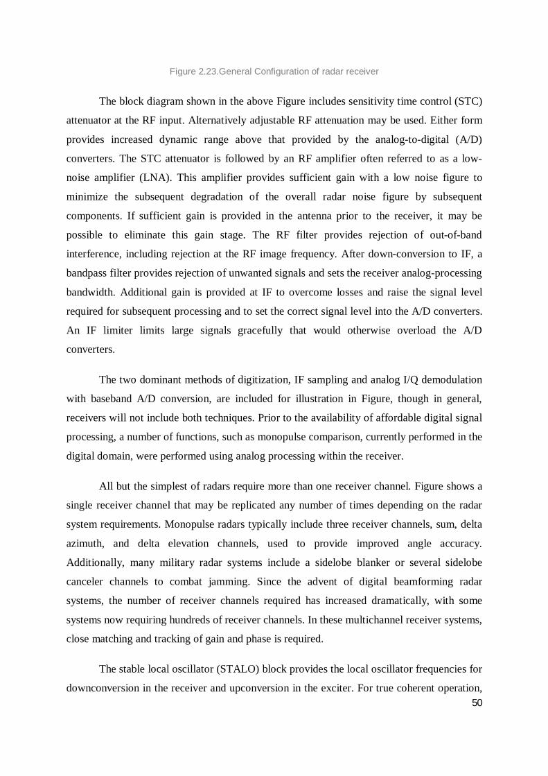
50
Figure 2.23.General Configuration of radar receiver
The block diagram shown in the above Figure includes sensitivity time control (STC)
attenuator at the RF input. Alternatively adjustable RF attenuation may be used. Either form
provides increased dynamic range above that provided by the analog-to-digital (A/D)
converters. The STC attenuator is followed by an RF amplifier often referred to as a low-
noise amplifier (LNA). This amplifier provides sufficient gain with a low noise figure to
minimize the subsequent degradation of the overall radar noise figure by subsequent
components. If sufficient gain is provided in the antenna prior to the receiver, it may be
possible to eliminate this gain stage. The RF filter provides rejection of out-of-band
interference, including rejection at the RF image frequency. After down-conversion to IF, a
bandpass filter provides rejection of unwanted signals and sets the receiver analog-processing
bandwidth. Additional gain is provided at IF to overcome losses and raise the signal level
required for subsequent processing and to set the correct signal level into the A/D converters.
An IF limiter limits large signals gracefully that would otherwise overload the A/D
converters.
The two dominant methods of digitization, IF sampling and analog I/Q demodulation
with baseband A/D conversion, are included for illustration in Figure, though in general,
receivers will not include both techniques. Prior to the availability of affordable digital signal
processing, a number of functions, such as monopulse comparison, currently performed in the
digital domain, were performed using analog processing within the receiver.
All but the simplest of radars require more than one receiver channel. Figure shows a
single receiver channel that may be replicated any number of times depending on the radar
system requirements. Monopulse radars typically include three receiver channels, sum, delta
azimuth, and delta elevation channels, used to provide improved angle accuracy.
Additionally, many military radar systems include a sidelobe blanker or several sidelobe
canceler channels to combat jamming. Since the advent of digital beamforming radar
systems, the number of receiver channels required has increased dramatically, with some
systems now requiring hundreds of receiver channels. In these multichannel receiver systems,
close matching and tracking of gain and phase is required.
The stable local oscillator (STALO) block provides the local oscillator frequencies for
downconversion in the receiver and upconversion in the exciter. For true coherent operation,

51
the STALO is locked to a low frequency reference, shown by the reference oscillator in
Figure 6.1 that is used as the basis for all clocks and oscillators such as the coherent local
oscillator (COHO) within the receiver and exciter. The clock generator provides clocks to the
A/D converters and the direct digital synthesizer and provides the basis for the signals that
define the radar transmit and receive intervals.
Almost all modern radar systems use digital signal processing to perform a variety of
functions, including pulse compression and the discrimination of desired targets from
interference on the basis of velocity or the change in phase from one pulse to the next.
Previously, pulse compression was performed using analog processing with dispersive delay
lines, typically surface acoustic-wave (SAW) devices. Analog pulse compression has largely
been replaced by pulse compression using digital signal processing.
2.4. Some Limitations
We have seen in above discussion that in case of coherent radar the information is
extracted from the change in the phase of the signal. So, in order to get good performance
phase stability requires. It can be seen that there is mixing or frequency multiplication
process involve in radar system both in case of up-conversion and down-conversion. This
mixing process is actually a main source of phase noise in radar; it adds the frequency
fluctuations and hence leads to errors. So, 1st thing we need is to get rid of this block. The
other limitation is the processing speed of electronics which ultimately affects the
performance of modern system. In radar receiver ADC involves, but electronic ADCs are
limited in sampling rate and resolution (detail is in next chapter) which limits the realization
of fast system.

52
3. Photonic based Radar:
Characterization of 1x4 Mach-
Zehnder Demux
In this chapter the scheme that has been used to implement the optical transceiver for
a photonic assisted fully–digital radar system, based on optic miniaturized optical devices
both for the optical generation of the radio frequency (RF) signal and for the optical sampling
of the received RF signal, will be discussed. The focus will be mostly on the receiver side,
especially on demux which is a critical block of the receiver. The architecture of optical radar
is under experimental phase. The scheme for the generation of RF signal has been
implemented with desired results and now experiments on receiver are being carrying out.
3.1. Overall Scenario
There are two main portion of the transceiver used to implement fully digital optical
radar, one portion is to generate the radio frequency (RF) for radar by exploiting photonic.
The other portion is the receiver side in which sampling of the received RF radar signal will
be performed in photonic and then these samples will be further processed to get the required
information. The proceeding discussion will be on these two portions.
3.1.1. Radio Frequency (RF) generation

53
In last chapter it is mentioned that coherent radar extract information from the phase
of the echoes, so it can be concluded that for coherent processing of radar phase noise should
be reduced as much as possible for better detection. Phase stability can be attained if we can
remove the up-conversion in the transmitter. Photonic solutions have been proposed recently
to avoid up-conversion in RF generation but these solutions don’t provide a very stable RF
generation [16]. In order to improve RF stability, phase locking is necessary. A relatively
simple technique for generating phase locked laser lines is the mode locking of lasers: the
intrinsic phase-locking condition of the mode-locked laser (MLL) ensures an extremely low
phase noise of the generated RF signal. So, MLL can be used to improve the performance of
radar transmitter.
For radar transmitter the technique proposed in [16] is based on MLL, same sampling
MLL of receiver, and exploiting phase stability of it. The basic idea for generating a stable
radar signal is reported in below Figure 3.1.
Figure 3.1.Basic scheme for the generation of radar signal using
same MLL used in optical-sampling of receiver
The signal from MLL is split into two separate paths, where two different modes are
selected at v0 and N∆v with the help of filters. One mode on one path is modulated to shape
the radar pulse while the other mode on second path is frequency shifted. Frequency shift is
required to get RF signal at required high frequency as we are using one MLL for transmitter
and receiver at sampling rate. The two processed modes are then combined and detected in
photodiode. This will generate the beating at the frequency (N∆v + δv) or (N∆v - δv),
depending on the sign of frequency shift. There will be negligible increase of phase noise

54
w.r.t original MLL. The variant of this technique has also been proposed in which two
modes are filtered before splitting as shown below in Figure 3.2.
Figure 3.2.Advance scheme exploiting optical I/Q modulator
The benefit of this technique is that in this way we can use commercial available I/Q
modulator but in previous case we need custom built-in integrated photonic device to avoid
phase fluctuations. I/Q modulator can provide frequency shift as well as RF pulse modulation
as shown in above figure. DBPF (Double band-pass filter) should be used to select two
modes from MLL, an example of DBPF is Fabry-Perot filter followed by a suitable band-pass
filter. The two selected modes will are simultaneously sent to both arms of modulator. On
one arm the two modes are modulated by radar pulse while on the other arm a carrier-
supressed modulation driven by low frequency oscillator splits the two modes into new
spectral components at +/- δv from the original modes. The processed signals from two are
arms are combined and detected by photodiode where the beating of all these frequency
components occurs. A microwave filter can then filter out the desired signal produced by
beating.
In this case it will be easier to use tuneable filters; the only cost to pay in this
technique is the need for a microwave filter after photodiode, since it will filter the signal at
required frequency from the beating of frequency components at N∆v, (N∆v +/- δv) and
(N∆v +/- 2δv).
Experimental results
MLL at 9.953GHz has been used. Two adjacent modes (N = 1) are filtered and sent
them to I/Q modulator. A sine modulation at 47MHz is used for frequency shifting both the

55
lines. The RF pulse is a squared pulse, 1s pulse width over 3 s period. A RF filter at
10.0GHz is used to select the shifted signal. We first avoid the RF modulation to study the
carrier stability as shown in below Figures 3.3.
-150
-130
-110
-90
-70
-50
1.E+02 1.E+03 1.E+04 1.E+05 1.E+06
Offset Frequency [Hz]Ph
ase
Noi
se [d
Bc/
Hz]
-70
-60
-50
-40
-30
-20
-10
0
10
9880 9930 9980
Frequency [MHz]
Nor
mal
ized
Pow
er [d
B]
b)a)
Synthesizer @ 47MHz
Original carrier @ 9.953GHz
Shifted carrier @ 10.000GHz
Figure 3.3.a) Electrical spectrum after the photo-diode, radar pulse modulation is off, b) Phase noise
measure of the shifted carrier, compared with the original carrier and with 47MHz synthesizer.
Figure 3.3 a) above shows the electrical spectrum of the signal after the photodiode
when the radar pulse modulation is off and the shifting sinusoidal is on. Two shifted carriers
are generated around the original one at 9.953GHz. The figure demonstrates the generation of
a highly pure sinusoidal carrier, showing a side mode suppression of the carrier at 10GHz
greater than 50 dB. The phase noise of the shifted carrier is studied in next Figure 3.3 b),
where it is compared with the phase noise original MLL and of the 47MHz synthesizer. The
synthesizer shows a phase noise much lower than the original MLL; therefore the 10GHz
carrier shows a phase noise curve that largely follows original MLL. The two curves coincide
for the offset frequencies up to 100 kHz, while the shifted carrier shows the noise floor 5 dB
higher for higher frequency offset. Integrating the phase noise from 1 kHz to 1 MHz, which is
the frequency range of interest for radar application, an RMS jitter of 12 fs and 12.4 fs is
calculated for the original MLL and for the shifted carrier respectively. The remarkable small
difference in time jitter confirms that the frequency shift operation does not introduce
significant phase noise, allowing the generation of an ultra- stable RF carrier.
When applying the radar pulse modulation, the shifted carrier is modulated too and
the desire RF signal is produced. In Figure 3.4 a) the spectrum of the base-band radar pulse is
shown; the inset also reports the time trace of the rectangular radar pulse. Next Figure b)

56
shows the beating generated by the photodiode when the radar pulse modulation is active; the
three carriers shown are all modulated. In last Figure c) the spectrum of signal of interest at
10GHz after the microware filter is reported. The modulation spectrum correctly moved
around the shifted carrier, although the effect of microwave filter is visible. The inset also
shows the time trace at the oscilloscope as expected, the signal shows the envelope of the
radar pulse modulated by the carrier at 10GHz.
Figure 3.4.a) Base-band spectrum (RBW=30kHz) and waveform (inset) of the radar pulse. b)
Spectrum (RBW=300kHz) of modulated carriers, after the photodiode. c) Spectrum (RBW=30kHz) and waveform (inset) of filtered radar signal.
In [17] a phase modulated RF signal generation with pulse compression technique in
coherent radar has been reported to increase the resolution of radar. Pulse compression is
demonstrated by utilizing Barker code.
3.1.2. Radar Receiver
As discussed in RF signal generation about up-conversion as source of phase noise,
similarly current electronic receiver for coherent radar use down-conversion by mixing the
received signal with local oscillator. This mixing process leads to phase instability, so we
need a technique to avoid down-conversion as well. By using photonic assisted analog-to-
digital converter technique we can avoid this down-conversion process. The received signal
is directly converted to digital form then analysed. Moreover currently available electronics
ADCs are limited in resolution (Effective Number of Bits (ENOB)) and sampling rate which
can be tackled very efficiently in photonic ADCs.
The rate-of-improvement of high-speed electrical ADCs is substantially slower than
that of digital signal-processing (DSP) hardware. The electronic ADCs are not able to fulfil
the requirements of high resolution which is needed in modern systems like radar. The

57
resolution of electronic ADCs is limited, in addition to the inherent quantization noise, by a
number of mechanisms including thermal noise, sampling aperture jitter, and comparator
ambiguity [2]. The equations [2] that calculate the associated maximum achievable
resolutions, in SNR-bits, are
thermal noise (referred to the input):
Bthermal = log2 (VFS2 / 6kTRefffsamp)1/2 – 1
where, VFS = Full scale voltage, Reff = Thermal noise resistance, k = Boltzmann’s constant
(1.380658 x 10⁻²³ J/K) and T = temperature in Kelvin
aperture uncertainty:
Baperture = log2 (2 / √3πfsampτa) – 1
Or
ENOB = log2 (2 / √3πfsampτa)
where, τa = RMS aperture jitter (standard deviation of the variation of the sampling point,
sampling jitter)
comparator ambiguity:
Bambiguity = (πfT / 6.93fsamp) – 1.1
where, Bambiguity reflects the probability that the comparator will make an ambiguous decision
From above expressions SNR curves, shown in the below Figure 3.5, are calculated in [2] for
values of thermal noise, aperture jitter, and fT which measures comparator ambiguity.
Assume VFS = 1V, T= 300 K for the thermal noise curves. Aperture jitter is calculated for
Nyquist sampling, i.e. fsig = fsamp / 2. Comparator ambiguity is determined from the
regeneration time constant of the IC technology.

58
Figure 3.5.Survey ADCs
It can be observed from above curves that thermal noise appears to dominate the
performance of high-resolution low-bandwidth ADCs while aperture jitter and comparator
ambiguity become important at high sampling rates. The current state-of-the-art is limited by
the equivalent of thermal noise associated with a ~2 kΩ resistor for sampling rates under 2
Ms/s. Aperture jitter, in the range 0.5 ps to 2 ps, limits SNR for the sampling frequency range
of ~2 Ms/s to 4 Gs/s. Comparator ambiguity is limited via the regeneration time constant
corresponding to a value of fT ~ 50 GHz for ADC’s at the highest sampling rates. So, it can
be concluded that in order to attain high resolution high sample rate ADCs, aperture jitter and
comparator ambiguity has to be reduced.
Let’s assume that jitter is the only error source, Figure 3.6 below shows the allowable
timing jitter for a Nyquist ADC (i.e., maximum input frequency (fsig) = 1/2 sampling rate
(fsamp)) as a function of sampling rate and effective bits [18]. Estimates of aperture jitter in
state-of-the-art electronic ADCs range from 0.5 to 2 ps (see hatched region in below Figure),
indicating that electronic aperture jitter is presently a major limit to the performance of high-
speed high-resolution ADCs [18]. For example, the 50-fs timing jitter required to implement
a 1- GS/s 12-bit converter is far below that of present electronic jitter estimates. In contrast,
sampling-aperture jitter less than 50 fs has been attained in optical sampling systems.

59
Figure 3.6.Timing-jitter requirement for ADCs as a function of sampling rate and number of effective
bits. The calculation assumes that timing jitter is the only noise source.
From the developed arguments given in above paragraphs it can be concluded that 1st
of all we needed a technique to attain very low (fs) timing jitter which will result in high
resolution ADC. A very attractive solution to get low timing jitter is to sample the signal in
Photonic domain using mode-locked laser. The principal advantages of optical sampling are:
1) modern mode-locked lasers can produce high-frequency ( 10 GHz) periodic sequences of
optical pulses with timing jitter significantly below that of electronic circuitry, and 2) the
sampling process can be made to be highly linear with negligible back-coupling between the
optical sampling pulses and the electrical signal being sampled. The timing jitter of actively
mode-locked fiber lasers has been measured to be 10 fs over narrow-band integration limits
(100 Hz to 1 MHz) and 50 fs pulse to pulse (see hatched region in Figure 3.6).
In our radar receiver we are sampling the received radar signal in photonic domain to
get the benefit of low timing jitter in sampling and then utilizing well developed electronics
technology for quantization to minimize the cost as well. Our aim is to get ENOB value of
10bits.
3.1.2.1. Photonic Sampled and electronically Quantized ADCs
Mode-locked laser can be used to sample an RF signal was discussed first by H. F.
Taylor, M. J. Taylor, and P. W. Bauer in Applied Physics Letter (1978) as part of their all-
optical ADC. Later, Bell et al. (1989) recognized that optical sampling and temporal
demultiplexing would be useful for making a time-interleaved ADC. In 1989 1st they had

60
analysed and indicated that precision of 6 bits should be attainable by a system which
includes an actively mode-locked diode laser operating at 4 GHz (4GS/s), and a 1x8 time
demultiplexer. Then in 1991 they had demonstrated a system which uses 4 parallel electronic
A/D converters and a pulsed diode laser with a sample rate of 2 GHz. The precision of this
system is as high as 2.8 effective bits. After that, many researchers (1992 - 2004) have
concentrated on the optical sampling process alone without demultiplexing to take advantage
of the short pulse widths and low pulse-to-pulse jitter of a mode-locked laser. The basic
components of an optically sampled system consist of a stable pulsed laser, an optical
modulator, and a detector/integrator [19] as shown in Figure 3.7 below.
Figure 3.7.Photonic sampled and electronically quantized ADC.
In optically sampled ADCs, the optical pulse generator is typically a mode-locked
fiber or semiconductor laser, the optical modulator is typically a LiNbO3 Mach- Zehnder
modulator, and the detector is a high-speed photodiode. This system contains an analog
optical link and thus its performance is characterized by the link SNR, SFDR, modulator
bandwidth and modulation index, photodiode saturation current and bandwidth [19].
The technique to implement ADC for our radar receiver is based on the very
impressive work done in [18] to attain resolution of 10bits with fast sampling rate. The block
diagram of the scheme is given in below Figure 3.8:

61
Figure 3.8.Generic architecture of an optically sampled time-interleaved ADC
There are three main components in the above mentioned scheme:
1. Mode Locked Laser (MLL): to get low jitter train of pulses at required rate for sampling.
2. Electro-optic Modulator: to sample received radar signal with precisely timed optical
pulses from MLL that converts electrical signal variations into optical-pulse intensity or
energy variations.
3. Optical Demux (OTDM): to parallelize the post-sampled pulses so as to meet the
processing speed of electronic ADC used for quantization. In short demux is used to rate
reduced the sampled pulses.
Figure 3.9 shows different components used in receiver. To implement the photonic
sampling process MLL having repetition rate of 400MHz with 1ps pulse width has been used
to generate 400MS/s. The received RF radar signal at 9900MHz will be sampled by using
LiNbO3 Mach Zehnder Modulator (MZM). This MZM will convert the electrical signal
variations into amplitude-modulated optical pulses at the rate corresponding to MLL. Then
optical 1x4 demux, clocked at 200MHz and 100MHz, used to parallelize the post sampled
pulses to rate reduce the sampling rate at 100MHz to meet electronic speed of ADC. The
further detail about optical demux will be given later. One thing which is worth mentioning is
the use of Dispersion Compensation Fibre (DCF) before photodiode. The optical peak power
limits the power at the photodiodes, and hence the amplitude of the signal at the ADC. The
DCF is used to broaden the pulse and hence increase the efficiency.

62
Figure 3.9.Components of radar receiver scheme
3.2. Characterization of 1x4 Mach-Zehnder Demultiplexer
(demux)
Optical demux is a very critical block of the receiver used for the parallelization of the
optical samples, by employing optical time division demultiplexing, and it strongly impacts
the performance of the whole system. While the linearity and dynamic range of an A/D
converter can be enhanced by employing optical sampling, the sampling rate is limited by the
speed with which the associated electronic A/D converter can quantize the detected optical
pulses. An attractive means for increasing the sampling rate and on the same time to meet
electronic processing speed is to use a 1: M demux at the output of the electro-optic
modulator to direct sequential optical pulses to a parallel array of electrical A/D converters
each operating at a quantization rate of fsamp/M where fsamp is the aggregate sampling rate. We
are using time-division demultiplexing technique to parallelize the samples. The input pulses
are all at the same wavelength i-e at 1550nm. The demux consists of an array of electrically
driven optical switches (e.g., a cascade of 1 x 2 electro-optic switches) that direct the
sequential optical pulses to the appropriate detectors and electronic A/D converters.
In order to realize a demux we need a design which can fulfil all the system
specifications. The solution should be compatible with the Mach Zehnder modulator (used
for sampling) and the final photo-detector technology, enabling a higher level of compactness
of the whole system. The frequencies of interest for this application are lower than few GHz
for the sampling rate and hundreds of MHz for the parallel sampling flows, making the
chosen technology an appropriate solution, able to guarantee low noise, low attenuation and

63
high sensitivity. Beside this, we also took into consideration the low cost factor, complexity
and integration. A 1x4 demux has been developed using Mach Zehnder Interferometers, an
electro-optic solution, as a switch matrix. Mach Zehnder can be precisely controlled to attain
the stability and also provide high extinction ratio to minimize cross-talk between channels.
Cross- talk adds spurs in the signal. Due to the integrated structure sufficient stability as well
as balanced path to provide correct synchronism between optical and electrical control signals
can be attained. So, a 1x2 Mach Zehnder switch has been used in two stages to get 1x4
demux as shown in below schematic.
Figure 3.10.MZ switch matrix
3.2.1. Technological aspects
The MZM chip is realised in integrated optics on LiNbO3, the optical waveguides are
realised in Thermal Annealed Proton Exchange (TAPE) technologies that allows a higher
optical power damage threshold with respect to Ti diffusion. The thin film electrodes are
defined by deep UV photolithography, the microwire thermosonic bonding allows the
electrical interconnection in the package and also the SM fiber pigtail is implemented. An
example of packaged device is shown in Figure 3.11

64
Figure 3.11.Packeged demux
The 3 MZM modulators allow the dual output modulation as shown in Figure. 3.12.
The optical couplers are electro-optically tuned in order to achieve an optimum optical
extinction ratio (Er) of the MZM and to provide more control. To operate the MZM in any
working point (and particularly for quadrature point), a bias voltage is needed on the RF
electrode, and then the device should be equipped with bias-T circuit.
Figure 3.12.Internal structure of MZ
In order to reduce the rate of 400MHz post sampled pulses to 100MHz, we need a
clock of 200MHz at the RF port of 1st stage of demux to obtain pulses at 200MHz. Then RF
ports of the second stage will be provided with clock of 100MHz to get pulses at 100MHz.
This clock will be provided by dividing the MLL output by 2 and 4 to get 200MHz and
100MHz pulses respectively. Figure 3.13 shows the signal definition before and after demux.
There is a phase change of 900after 1st stage.

65
Figure 3.13.Signal definition before and after demux
For these RF signals we need to match the impedance and along this we need to
develop bias-T to provide DC as well.
3.2.2. Mach Zehnder as Switch
Among different topologies, MZI structures are most efficient, converts a phase
modulation into an intensity modulation, which is widely used for many optical applications
e.g. modulators etc. Monolithically integrated MZI switches represent the most promising
solution due to their compact size, thermal stability and low power operation. Basic 2x2 MZI
switch structure can be viewed, as shown in Figure 3.14 below, as two interferometric arms
of equal length connecting two couplers. The first coupler is used to split the signals in two
beams, which when passed through the interferometric arms experiences phase difference.
This phase difference is due to voltage variations across electrodes covering interferometric
arms that in turn changes refractive indices. Finally, both the beam with different phases are
put together again into a single signal by the second coupler, and the outputs are observed as
per constructive or destructive interference.

66
Figure 3.14.2x2 MZ switch layout
In our case we need a switch with one input so we have used MZI with one input
close. The input signal will be split among two waveguides and then undergo the phase
change due to applied voltage. When the signal will be combined in the coupler, an electro-
optic, then there will be a destructive interference on one port and constructive interference
on the other port to output the optical signal only from one of the outputs at one time.
3.2.3. Matching and Biasing network
Impedance matching is needed to provide maximum power transfer between the
source or RF energy and its load. The first reason for matching is just power efficiency. The
second reason is device protection. If RF circuit is not matched we get reflected power. This
reflected power builds standing waves on the transmission line between the source and load.
Depending on the phase between the forward and reflected both waves can either subtract or
add. Because of that on the line we can get places where the voltage is the sum of either
voltages or eventually places where the voltage equals zero (maximum current). For RF
input, as in our case, the condition for impedance matching is that real part of the impedance
should be equal to the real part of the load and reactance should be equal and opposite in
character. For example if our source impedance is R + jX to achieve matching our load
should be R – jX.
Following are the demux specifications to match:

67
Input reflection coefficient @ 100 MHz S11 = 0.976exp (-j0.209) corresponding to
load impedance of z = 476.5exp (-j1.45) Ohms.
Input reflection coefficient @ 200 MHz S11 = 0.986exp (-j0.327) corresponding to
load impedance of z = 302.9exp (-j1.52) Ohms
All the impedances are matched against source resistance of 50 Ohms. The circuit diagram
used to build the matching and biasing network is shown below along with the developed
matching network.
Figure 3.17.Matching and biasing network circuit diagram and packaged device
The magnitude of scattering parameter, at 200MHz and 100MHz, after impedance matching
is shown below in two graphs. These graphs have been taken by mean of network analyzer.
The dips in these graphs at 200MHz and 100MHz clearly depict low magnitude of scattering
parameter which is the need of scheme.

68
Figure 3.16.Magnitude of S11 parameter at 200MHz after impedance matching
Figure 3.17.Magnitude of S11 parameter at 100MHz after impedance matching
After matching the impedance we need to find different voltage values to control
demux and to get required results. As described above that optical signals from two MZ arms
are coupled using electro-optic coupler. So, we need to find the voltages (Vbias coup) to
control the coupler and to operate the coupler accordingly.
3.2.4. Coupler Bias Voltage (Vbias coup)

69
The electro-optic coupler is an important application of electro-optic effect use to
control the optical devices. This can be used to transfer the light from one waveguide to the
other, so that the device serves as an electrically controlled directional coupler. Two
parameters govern the strength of this coupling process: the coupling coefficient C (which
depends on the dimensions, wavelength, and refractive indices), and the mismatch of the
propagation constants ∆β = β1 – β2 = 2π∆n/λ0, where ∆n is the difference between the
refractive indices of the waveguides. The coupling efficiency can be controlled by external
voltage level applied through the electrode as shown in Figure 3.18. The applied voltage will
determine the amount of optical power transmitted to a particular output port.
Figure 3.18.Schematic of electro-optic coupler
A dependence of the coupled power on the phase mismatch is the key to making
electrically activated directional couplers. The power transfer ratio in phase mismatch case,
β1 ≠ β2, is T = P2(L0)/P1(0) which depends on phase mismatch parameter, ∆βL0 where, L0 =
π/2C. Here the ratio is based on one input P1(0) in one of the waveguide, same theory can be
applied on other input also. Now the power transfer ratio is:
T = (π/2)2 sinc2 {1/2[1 + (∆βL0/ π)2]1/2}
The ∆β of the phase mismatch ∆βL0 can be controlled by mean of electro-optic effect. This
leads to the dependency of T on applied voltage V and T becomes:
T = (π/2)2 sinc2 {1/2[1 + 3(Vbiascoup/Vs)2]1/2}
where, Vs is switching voltage

70
Now what we need to find an operating voltage Vbiascoup where the coupling will be
50/50 i-e T should be one half. This means that half power from any of the waveguide will
remain in the same waveguide and half will transfer to the other waveguide. This implies for
both of the input signals. In order to find coupling bias voltage, Vbiascoup, we need to control
bias Voltage of each MZ and then to measure the extinction ratio at the output ports of the
demux. To find the Vbiascoup following setup has been made:
Figure 3.19.Experimental setup to find Vbiascoup
The way to find Vbiascoup was:
1. Consider one coupler at one time and apply different values of Vbiascoup to that
coupler e.g to coupler 3 at DC 3.
2. For each value of Vbiascoup applied, vary the Vbias of respective MZ, e.g MZ3 in case
of coupler3, and for each value of Vbias measure the output power from the respective
ports, port 3 and 4 in case of MZ3. The voltages to all other couplers and MZ will be
adjusted to get high output power.
3. Then Extinction Ratio (Er) has been measured at each Vbiascoup point. After that all
the results are compiled to find 50/50 coupling Vbiascoup and Er at that voltage.

71
In order to measure the coupler bias a program has been made on LabView to provide
different voltages by controlling the voltage supply and then reading the output power from
power meters. The voltage supplies and power meters have been controlled through the
program made in LabView. There is different sequence of coupler bias and MZ bias values
that has to be provided to one MZ at one time. There are two loops that are controlling the
voltage supplier. The outer loop provide different values of Vbiascoup and for each value of
outer loop the inner loop will provide Vbias to the MZ which is under observation, provided
all the other coupler and MZ biases are adjusted at the values where output power is
maximum. The next step is to measure the output power from demux ports. This has been
done by controlling two power meters by mean of LabView. In this case we were able to find
Er of output optical signal from different ports and then to find the operating point of
couplers.
A number of experiments have been carried out in the Lab with above mentioned
setup and then results have been collected and observed. Due to the effect of temperature on
MZ the experiments have been carried out on different temperature values. The temperature
of MZ has been controlled by temperature stabilizer. Below is the description of the
experiment results that has been taken.
Temperature 27 oC
Below is the graph, Figure 3.20, that is showing the Er of output optical signals versus
Vbiascoup at 27 oC temperature for MZ1 (at stage one of demux). The output has been
collected from port2 (one output port from MZ2) and port3 (one output port from MZ3) and
the coupler and MZ bias voltages have been provided on DC1 and MN1 (follow Figure 3.18
for better understanding) respectively.

72
Figure 3.20.Coupler bias vs Output Er for coupler1 of MZ1 at temp. 27
By observing the above output graph the coupler bias voltage of 1st coupler for 50/50
coupling comes out to be -17 V at extinction ratio of almost 25 dB.
For coupler2 Vbiascoup has been provided at DC1 port and MZ2 bias on MN2. The
output power has been measured from port3 and port4. The bias voltages of other couplers
and MZs have been set on the fixed voltages. The graph for coupler2 is shown below, Figure
3.21. The graph shows that 50/50 coupling voltage is at -22 V and extinction ratio of output
optical signal from two ports at that voltage is almost 23 dB.
Figure 3.21.Coupler bias vs Output Er for coupler2 of MZ2 at temp. 27

73
Now for the last coupler i-e coupler3, Vbiascoup has been provided at DC3 port and
MZ3 bias on MN2. The output power has been measured from port1 and port2. The bias
voltages of other couplers and MZs have been set on the fixed voltages. The graph for
coupler3 is shown below. The graph shows that 50/50 coupling voltage is at -22.6 V and
extinction ratio of output optical signal from two ports, at that voltage, is almost 23 dB.
Figure 3.22.Coupler bias vs Output Er for coupler3 of MZ3 at temp. 27
Now to check the effect of temperature on demux some series of experiments have
also been performed on different temperature i-e at 22 oC and then collect the results. The
procedure applied is the same as above but the results are different as shown in below graphs.
Temperature 22 oC
From the below graph, the coupler bias voltage for coupler1 is -19.9 V and the
extinction ratio is almost 26 dB. This shows that due to the change in the temperature the
voltage shifted as compared to the previous value of the same coupler.

74
Figure 3.23.Coupler bias vs Output Er for coupler1 of MZ1 at temp. 22
The coupler bias voltage for coupler2 is -25.9 V and the extinction ration is almost
22.7 dB as shown in the below graph. This also shows the shift in the voltage.
Figure 3.24.Coupler bias vs Output Er for coupler2 of MZ2 at temp. 22
The coupler bias voltage for coupler3 is -21.2 V and the extinction ration is almost
23.6 dB as shown in the below graph. If this voltage value is compared with the previous

75
value taken at different temperature of the same coupler, shift can also be observed due to the
temperature.
Figure 3.25.Coupler bias vs Output Er for coupler3 of MZ3 at temp. 27
3.2.5. Critical Observations
In order to check the stability of demux over temperature, different experiments has
been performed on the same coupler and MZ at the same temperature. The graph of only
MZ2 at 27 oC temperature are shown below, consider also the graph of MZ2 giving -22V and
ER 23dB at 27 oC temperature showed above. For each new experiment the values for
coupler and MZ bias has been changed but temperature is fixed. It is observed that there is a
drift in 50/50 coupling voltage, which means un-stability.
Figure 3.26.Drift in coupler bias voltage at same temperature

76
The reason can be that the temperature of the crystal doesn’t remain stable. We have
used the temperature stabilizer but it is not able to stabilize the temperature of the crystal to
large extent. In order to reach the high extinction ratio requirement i-e more than 30dB, we
need stabilize coupling and MZ bias. This temperature instability will also affect the
quadrature bias voltage of MZ and hence the extinction ratio. At-last it is worth mentioning
here that in order to stabilize the bias we can’t even use the Bias Control Loop circuit (BCL)
because it works if the modulation is zero mean. In our case the driving (clock) signal is
synchronous with the optical signal, so the mean output power will be different from different
outputs.
The next step in the characterization is to find the Vπ and then the bias voltages for
each MZ involve in the demux. To calculate this value we need the driving signal and for that
we need frequency dividers and low noise amplifiers which should be precisely tuneable to
meet the phase (90o shift at 200MHz) and gain requirement. To reach an ENOB of 10 bits the
time/amplitude jitter of the demux must be less than 30dB.
∆amp = cos2(∆ V/ Vπ)
To have ∆amp < 0.1% the voltage error must be lower than 2%. The amplitude error
is also due to the time jitter, so it’s better stay below 1%. Moreover, to reach 30dB ER, the
error on the Vπ measure must be less than 2%.

77
4. Conclusion
In order to summarize the whole work, the results that have been taken during a series
of experiments allow us to check the performance of the demux and to find the issues
regarding the control of demux which will lead to the bases for the next work in photonic
assisted radar research. As far as impedance matching is concerned the required results have
been met. Regarding the control of the demux, it can be finally concluded that we can attain
what we are looking for if it is controlled well. By following the coupler bias vs Er curves, in
the last chapter, it can be concluded that demux can give high Er if it is controlled well. There
are some issues, regarding the instability, in the control of demux which should be addressed
and can be covered if tuned well. Experiments on demux are still going on in the Lab; below
I will mention what is the current status of the experiment.
4.1. Current Status of Experiments
The experimental setup on which current activities has been performed is shown in
the Figure 4.1 below. In this preliminary activity all the control parameters have been
manually adjusted in order to obtain the best performance and compensate some unexpected

78
problems, like the phase ambiguity of the clock dividers and stability. In our scheme both the
200MHz and the 100MHz driving signals are obtained by a division of the MLL’ clock at
400MHz, so they apparently can’t be locked in phase.
Figure 4.1.Experimental setup
Now the experiments have been performed by considering the deriving signals as well
and for that low noise amplifiers (LNA) have been designed. Rest of the text will be on
designing of LNAs and latest experimental results.
4.1.1. Driving Signal amplification and tuning
In order to provide the driving signals to the switching matrix, two different types of
electrical amplifiers have been designed and realized: one single input double output 100
MHz low noise amplifier and one 200 MHz single input single output amplifier. Peculiar
characteristics of the designed amplifiers are the very precise tunability of the operative gain
and of the phase of the output signals. In Figure 4.2 and Figure 4.3 the electrical schemes of
the two amplifiers are shown.

79
.
Figure 4.2.Single Input double output low noise 100 MHz amplifier
Figure 4.3.Single input single output low noise 200 MHz amplifier
The design specifications of the two amplifiers are listed in the table below:

80
Both amplifiers are based on a low noise and high gain Bipolar Junction Transistor
(BJT). Due to the operational constraints of the optical de-multiplexer a precise tuning of the
amplifiers gain and of the output phase is needed. The gain, can be finely tuned, thanks to the
small tuning range needs, by slightly changing the working point of the BJT, without
affecting significantly the noise figure NF of the device, that is, in all the tuning range, lower
than the design specifications. For what concern the phase tuning, this can be changed by
acting on the output matching network. The 100 MHz device provide also a 90° phase shift
between the two outputs, in order to match the shift requirement for the driving signals of the
second stage of the switching matrix.
4.1.2. Experiment Results
The current experimental results reported has led to an effective number of bit
(ENOB) equal to 5.27, while the targeted ENOB was >8. The obtained number is largely
limited by the reduced dynamic range of the sampled pulses at the ADC, which only cover
11mV out of 200mV (minimum input range for the ADC). The second cause for reduced
ENOB is the noise generated in the optical and electrical amplification stages.
On the other hand, the FFT spectrum in below Figure 4.4 does not show the spurious
components that characterize the sampling processes affected by crosstalk. This suggest the
correct behaviour of the switch matrix, even if it is used here as a demultiplexer.

81
Figure 4.4.Spectrum of the reconstructed signal.
The next activity will be to fully exploit the switching functionality of the matrix,
setting all the bias voltages and optimizing all the driving signals.

82
5. References
1. R. Rzemien, “Coherent Radar: Guest Editor’s Introduction,” John Hopkins APL
Technical Digest, 1997.
2. R. H. Walden, “Analog-to-Digital Converter Survey and Analysis”, IEEE J. Sel. Areas
Commun., vol 17, no. 4, pp. 539-550
3. Le Nguyen Binh, “Photonic Signal Processing, Techniques and Application”.
4. http://www.ntt.com/worldwide/resource-center/article/data/global-watch02.html
5. S. J. Ben Yoo, Fellow, IEEE , “Energy Efficiency in the Future Internet: The Role of
Optical Packet Switching and Optical-Label Switching”, IEEE Journal of Selected
Topics In Quantum Electronics, Vol. 17, No. 2, March/April 2011
6. Shacham, A.; Small, B.A.; Liboiron-Ladouceur & O.; Bergman, K., (2005). A fully
implemented 12x12 data vortex optical packet switching interconnection network. IEEE
Journal of Lightwave Technology, Vol. 23, No. 10, (Oct. 2005) pp. 3066-3075, 0733-
8724.
7. K. Wilner and A.P. van der Heuvel, “Fiber-optic delay lines for microwave signal
processing”, Proc. IEEE, 64(5), 805–807, 1976.
8. M. Scaffardi, P Ghelfi, C. Porzi, G. Meloni, G. Berrettini, A. Malacarne, F. Fresi, E.
Lazzeri, J. Wang, X. Wu, I. Fazal, A. Willner, L. Potì, A. Bogoni, “ Photonic Digital
Processing for Enabling Next Generation Optical Networks”, IEEE, 2009.
9. C. Porzi, et al, “All-optical NAND/NOR Logic Gates with Passive Nonlinear Etalon
Exploiting Absorption Saturation in Semiconductor MQWs”, IEEE 2007
10. R. H. Walden, “Analog-to-Digital Converter Survey and Analysis”, IEEE J. Sel. Areas
Commun., vol 17, no. 4, pp. 539-550

83
11. M. P. Fok, K. L. Lee, C. Shu, “4 x 2.5 GHz Repetitive Photonic Sampler for High-Speed
Analog-to-Digital Signal Conversion”, IEEE Photon. Technol. Lett., vol. 16, no. 3, pp.
876-878 March 2004.
12. http://www.radartutorial.eu.
13. Merrill I. Skolnik, “Introduction to Radar Systems”, 2nd Edition.
14. Mark A. Richards, James A. Scheer, William A. Holm, “ Principals of Modern Radar:
Basic Principals ”
15. Michael E. Yeomans, “Chapter 6 of Radar Handbook by Merrill Skolnik”.
16. Paolo Ghelfi, et al. “Ultra-stable Radar signal from a Photonics-Assisted transceiver
based on single Mode-Locking Laser”, OSA/OFC/NFOEC 2011.
17. Paolo Ghelfi, et al. “Photonic generation of Phase-Modulated RF signals for pulse
compression techniques in Coherent Radars”, IEEE 2011.
18. Paul W. Juodawlkis, et al, “Optically Sampled Analog-to-Digital Converters”, IEEE
Transactions on Microwave theory and Tchniques, VOL. 49, NO. 10, OCTOBER 2001.
19. George C. Valley,” Photonic analog-to-digital converters”, 2007 Optical Society of
America.