photonic band gap aperture coupled fractal shape tri …jpier.org/pierc/pierc69/13.16082901.pdf ·...
TRANSCRIPT

Progress In Electromagnetics Research C, Vol. 69, 125–138, 2016
Photonic Band Gap Aperture Coupled Fractal ShapeTri-Band Active Antenna
Tale Saeidi1, *, Idris B. Ismail1, Mojtaba Ahadi2, and Adam R. H. Alhawari3
Abstract—A modified Koch fractal shape is used to decrease the dimensions of an antenna andresonates at more than one band for agricultural application. A new feeding technique of aperturecoupled method called a non-uniform annular Photonic Band Gap is applied in order to integrate thedesigned antenna to the active elements. Subsequently, a transmission line transformer is designedusing Genetic algorithm to achieve a perfect matching between the active element (amplifier) and theload (antenna). The proposed antenna is designed and fabricated. The results show that the proposedantenna has a high gain of 20.5 dB, 21 dB, and 22 dB at 0.915 GHz, 1.8 GHz and 2.45 GHz respectivelywith a compact size and low cost. The results predict its prospect as a promising alternative to theconventional one, which is compatibly applicable to agriculture applications especially when multibandfunction is required.
1. INTRODUCTION
Nowadays, the product protection against pest in agriculture becomes a challenging problem, and thecooperation of the scientific fields to solve it is increasing. Therefore, protections of these productsbefore and after harvesting is a great concern. One of the most effective and destructive problems inthis matter is protecting them from grain insects. There are many strategies such as applying physicaland thermal methods, X-ray, microwave (MW) energy, etc. But among all these techniques, MW energywas a promising way to terminate the insects present in grain products. The most important reasonsthat forced the scientists to use the MW energy were having no chemical residues in food and thus noside effects on the human body. MW energy also does not have adverse impacts on the environmentaround. Insects cannot tolerate this treatment and even cannot continue developing [1–3]. Based onthe Federal Communications Commission (FCC), the approved frequency bands for this purpose are47.5 MHz, 915 MHz, 1.8 GHz, and 2.45 GHz. According to [4, 5], microstrip antennas can be utilized atmicrowave frequencies due to their small size, light weight, thin profile configuration, low fabricationcost, inclination to mass production, etc. [6, 7]. In order to decrease the cost of the antenna causedby its large dimensions, many techniques, such as changing and optimizing the shape of the antennato enhance the electrical length of the antenna, exploiting a substrate with high permittivity, usingreactive or resistive loading, and applying and altering notches or stubs positions on the patch, can beapplied as reported in [8]. Furthermore, there are some other ways that can be useful. For instances, thedefects in the patch metallization lead to noticeable radiator miniaturization. However, one can observethat such a technique decreases antenna resonant frequency, so antenna optimization is necessary. Anintegrating approach to antenna miniaturization involves the utilization of metamaterials. However, theuse of artificial materials leads to certain fabrication problems, and the design process becomes complex.
Received 29 August 2016, Accepted 21 October 2016, Scheduled 21 November 2016* Corresponding author: Tale Saeidi ([email protected]).1 Faculty of Electrical and Electronic Engineering, Universiti Teknologi Petronas, Malaysia. 2 Department of Computer andCommunication, Faculty of Engineering, University Putra Malaysia, Malaysia. 3 Department of Electrical Engineering, Facultyof Engineering, Najran University, Suadi Arabia.

126 Saeidi et al.
One of the solutions to above limitations can be reached by means of fractal curves. It hasbeen reported that the application of space filling fractal curves enables us to achieve considerableminiaturization and also wideband and multi-band properties [9, 10]. Hence, in order to optimize theshape of patch and not to face the aforementioned problems, a fractal shape can be used which wasfirst introduced in 1975 [11]. Currently, the fractal antenna geometries are widely utilized in manyapplications such as wireless communication systems due to their compact size, low cost, capabilityof multi-band operation, ease of feeding, wide bandwidth, multiband and low profile [12, 13]. Themost common fractal geometries which have been used in antenna designs are the Sierpinski gasket orcarpet fractal [14], Hilbert fractal [15], Minkowski [16], Square Curve fractals and Koch fractal [17]. Inmicrowave networks, matching the source and the load to the transmission line or waveguide is necessaryfor maximum power delivery [18]. Several works have been done to demonstrate different techniques ofmatching transformers for two arbitrary frequencies [19–21]. The Chebyshev filter, Genetic Algorithm(GA) and Particle Swarm Optimization (PSO) algorithm can be used in order to speed up the solvingprocess and optimize the results easily.
Passive antennas have some drawbacks compared to active antennas in radiating structures, andtheir gain and bandwidth are less [22]. Active antennas have several advantages such as increasingthe effective length of the antenna, enhancing the bandwidth, reducing the mutual coupling betweentwo array elements and improving the noise factor [23]. Active antennas can be made by integratingthe passive part with an active element as diodes or transistors [24]. Various interests in wirelesscommunication systems, incompatibility and efficiency have made a fast progress and growth in themicrowave and monolithic microwave integrated circuit (MMIC) technologies [25]. As an importantbuilding block in wireless systems, low noise amplifier (LNA) can be defined as a receiver’s performance.Generally, for designing the LNA, some considerations should be kept in mind, such as optimum inputmatching, optimum gain, low power consumption, high linearity and low noise figure [26].
In this work, a triple-band active antenna using fractal shape is presented for agricultureapplications. A non-uniform annular Photonic Band Gap (PBG) aperture coupled feed method isutilized to integrate the designed antenna to the active elements. Then, GA algorithm is used tomatch the active element (amplifier) to the load (antenna). Evidently, the proposed method makes thedesign method for active antennas simpler and more efficient. Finally, a high gain active antenna withhigh-quality performance is demonstrated.
2. PASSIVE ANTENNA DESIGN
Selecting the substrate material for an active antenna is a crucial factor that should be considered in theantenna design. The substrate selection should be done carefully; a thick substrate with low permittivityfor the patch layer to have better radiation efficiency and larger bandwidth and a thin substrate witha high permittivity for the feed line to shrink the undesired radiations and coupling [27, 28]. In thiswork, for radiator patch, four layers of RT Duroid 5880 with dielectric constant of 2.2 and thicknessof 0.787 mm is selected and stacked with each other using super glue with εr = 3.3. Moreover, anFR4 substrate with εr = 4.4 and a thickness of 1.6 mm as the thinner layer is used for the feed linewhich is integrated with the LNA circuitry. Four elements of modified Koch fractal shape compoundingwith a square loop [6] have been applied to reduce the antenna size and function as an antenna at threefrequency bands. As illustrated from Fig. 1, the proposed passive antenna includes a Koch fractal shapewhich has been modified as a patch, and seven shorting pins connect the patch to the ground where theantenna is fed by a 50 Ohm SMA connector. Table 1 indicates the dimensions of the antenna.
Table 1. Passive antenna dimensions.
Ls (mm) 70Lp (mm) 58.26Ws (mm) 70Wp (mm) 58.26W (mm) 3

Progress In Electromagnetics Research C, Vol. 69, 2016 127
(a) (b)
Figure 1. Prototype of the passive antenna, (a) top view and (b) perspective view.
First, a single element of 90-degree modified Koch fractal shape compounding with a circularlypolarized (CP) square loop microstrip line (Fig. 2) as a monopole antenna with a half-wave lengthaccording to the first resonant frequency (at 0.915 GHz) is designed. The modified Koch fractal isconstrained up to the second iteration only. Increment in iterations enhances the small edges mostly,which is practically useless in increasing the electrical length.
Figure 2. CP square loop microstrip line (a), the proposed modified Koch element compounded withCP square transmission line (b).
Then, to have more than one resonant frequency, the elements of the radiator patch are increasedto two, three and four elements. Based on the reasons explained before, a modified 90-degree Kochfractal shape antenna is compounded with the CP square loop microstrip line to decrease the antennaas much as possible.
Afterward, seven shorting pins (via) connect the patch to the PBG which plays as the aperturepart of the feeding technique (Aperture Coupled Feeding). The reasons behind using the shorting pinscan be seen in the next paragraph. The size of the patch can be reduced by using shorting pins. Inaddition, for further size reduction, the shorting pins are used as a loading in such a spot (location onthe antenna) where the electric field or current density is high at desired frequency. The shorting pinscan be located either at the edge or at the corner. For instance, a shorting pin at a corner of the patchgives us a maximum reduction in antenna size. Moreover, applying shorting pins at the edge of theradiating patch can yield a higher loading effects, and the resonant frequency is lower when the shortingpin is located at the edge and corner, thus maximum reduction of the antenna size is achieved at thislocation of shorting pin. However, a good reduction can be achieved by pin loading, but it reduces the
128 Saeidi et al.
gain and bandwidth (BW). In spite of the decrement in gain, BW can be compensated by applyingcompact antenna layers, aperture coupled feeding, etc.
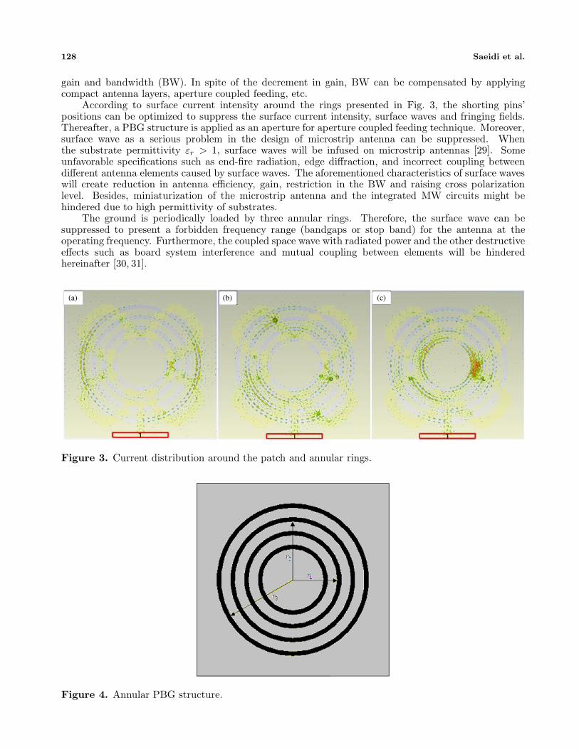
According to surface current intensity around the rings presented in Fig. 3, the shorting pins’positions can be optimized to suppress the surface current intensity, surface waves and fringing fields.Thereafter, a PBG structure is applied as an aperture for aperture coupled feeding technique. Moreover,surface wave as a serious problem in the design of microstrip antenna can be suppressed. Whenthe substrate permittivity εr > 1, surface waves will be infused on microstrip antennas [29]. Someunfavorable specifications such as end-fire radiation, edge diffraction, and incorrect coupling betweendifferent antenna elements caused by surface waves. The aforementioned characteristics of surface waveswill create reduction in antenna efficiency, gain, restriction in the BW and raising cross polarizationlevel. Besides, miniaturization of the microstrip antenna and the integrated MW circuits might behindered due to high permittivity of substrates.
The ground is periodically loaded by three annular rings. Therefore, the surface wave can besuppressed to present a forbidden frequency range (bandgaps or stop band) for the antenna at theoperating frequency. Furthermore, the coupled space wave with radiated power and the other destructiveeffects such as board system interference and mutual coupling between elements will be hinderedhereinafter [30, 31].
(a) (c)(b)
Figure 3. Current distribution around the patch and annular rings.
Figure 4. Annular PBG structure.

Progress In Electromagnetics Research C, Vol. 69, 2016 129
Three non-uniform ring-shaped patterns are etched from the ground layer with a period of ‘a’. Twomain parameters that should be well considered to obtain the stopband characteristics are the period‘a’ of the rings as a width of the rings and the filling factor ‘r/a’ (r is the radius of the rings). Ascan be illustrated from the following figure, ‘a’ is unchanged, and ‘r’ for each ring declines comparedto the first ring (first ring for first band operation) [32]. As can be seen in Fig. 4, the first ring (outerring) is the biggest, and it is related to 0.915 GHz, while the second (middle ring) and third (inner ring)are designed at the frequency of 1.8 GHz and 2.45 GHz, respectively. In accordance to surface currentintensity around the rings, the shorting pins’ positions can be optimized to suppress the surface currentintensity, surface waves and fringing fields.
3. ACTIVE ANTENNA DESIGN
After the passive antenna performance is designed and the result validated through simulation andmeasurement, it is tangible that the gain of the designed antenna is low and not applicable for thedesign purpose. Therefore, in this study, a surfacemount amplifier ‘LEE-39+’ as an active elementis used to enhance the gain of the designed antenna. Based on the amplifier’s data sheet [33], thisamplifier has an internal impedance equal to 50 and a gain of 22.3, 18.7, 14.7 dB at 0.915, 1.8 and2.45 GHz, respectively [33]. The real part of the input impedance of the designed passive antenna itself(Z11) at the operating frequency 0.915 GHz is 87 Ω, and it is not matched to the amplifier impedance.Consequently, an impedance matching circuit is presented to transfer the maximum power from theamplifier to the antenna. A three-section transmission line transformer (TLT) matching method isapplied to solve this problem (Fig. 5). To get the best and optimized values of every section of TLTfrom the simulation, two different optimizing methods are exploited apart from the analytical methodand Chebychev filter.
Figure 5. Three sections transmission line transformer [34].
As illustrated in Fig. 5, each section of the 3-section transformer consists of two variables, namelyimpedance (Z) and electrical length (βL). The analytical method presented in [35] is applied to get theactual values of every section, and then the Chebyshev filter technique reported in [18, 36] is appliedfor validation purposes. Afterward, two different algorithms are used to optimize the obtained values ofthe transmission line transformer specifications. First, Particle Swarm Optimization (PSO) algorithmis exploited to obtain the valid variables needed. To use the PSO for a given problem, each member inthe swarm is called a particle with assumed number of M = 50. The considered members exist in anN -dimensional solution space to alter their positions in accordance to either their last best performanceor the other particles’ best previous performance in the swarm. For every member in the N -dimensionalproblem, two M by N matrixes of a velocity (v) and position (x) are specified [26]. Here, PSO algorithmis performed using the assumed parameters as follows: M = 50, c1 = c2 = 2, Vmax = (1 + k)/2 wherek is the impedance transformation ratio, k = ZA/Z0. The stopping standard is that either a fitness(desired) value (in the simulation is considered less than 10−6) or a maximum number of 10,000 iterationsis reached. Furthermore, to have the final compact design, the following limitations are defined: lessthan λ1/4 for length of each section which is the wavelength at the first band design frequency. Asan initiation for PSO algorithm usage, the impedance and length values are randomly applied withthe intervals for impedances between ZA and Z0, and lengths between λ1/10 and λ1/4, respectively.Moreover, in the simulation process, f1, f2, f3, ZA, Z0 are considered constant and equal to 0.915 GHz,1.8 GHz, 2.45 GHz 87 Ω, 50 Ω, respectively. But the best solution cannot be achieved from the first run,thus, the simulation running continues more than 10 runs to approximately get the desired solution.

130 Saeidi et al.
Figure 6. Transmission line transformer circuit in CST design studio.
Figure 7. Front view of the proposed active antenna.
The second technique of the optimization is the Genetic Algorithm (GA). The details and requiredequations are presented in [34, 37]. After achieving the result values from each of the algorithms, theproposed active antenna is implemented using CST Design Studio as illustrated in Fig. 6. Obviously,the GA’s outcomes are the best among them because of the perfect matching and less spending timefor simulation and running as will be discussed in the next section. In the simulation, each section hasthe length in degrees, and it can be changed to mm, while the width in mm can be extracted fromimpedance in Ohm [35].
Subsequently, the simulated results of the modified Koch fractal active antenna and TLT circuitare validated, and the proposed design of TLT is fabricated. As a next step, the feeding layer should bechanged to a new one with the TLT matching circuit and the amplifier [28]. These steps of the wholesimulation can be seen in Figs. 7 and 8, respectively.
Later, the measurement process is divided into two parts. The first part is to measure the S-parameters, and the second one is to measure the gain of the antenna. For measuring and validatingthe simulation outcomes, a Vector Network Analyser (model: Anritsu 37347D) with a frequency rangeof 40 MHz–20 GHz is used. At the beginning of the measurement process, one port calibration method isperformed based on partial Thru-Reflect-Line (TRL) with the VNA in accordance to Agilent’s standards(short, open and terminator) using calibration kit model 3652. Then, the measured results are comparedwith the simulated ones. To measure the gain of the antenna, the method presented in [38] is utilized.In each measurement process, the proposed antenna is connected to the transmitter, which is a SignalGenerator (model: Anritsu-MG3700A) with the frequency range of 250 KHz–3 GHz, and antenna witha known gain is connected to a receiver, which can be a Spectrum Analyser (model: ADVANTESTR3267) with a frequency range of 100 Hz–8 GHz. The results are presented in the next section.

Progress In Electromagnetics Research C, Vol. 69, 2016 131
Figure 8. The feeding view of the proposed active antenna with TLT circuit.
(a) (b)
Figure 9. Photograph of the fabricated passive antenna. (a) Top layer and (b) bottom layer.
4. RESULTS AND DISCUSSION
4.1. Passive Antenna
The proposed antenna performances are investigated and simulated using CST simulator in terms ofgain, radiation efficiency, and reflection coefficient. After choosing the most applicable feeding type forthe antenna, it is integrated with the active component. To achieve this, the substrate thickness ofthe patch layer should be thicker with less permittivity. Fig. 9 shows photos of the fabricated passiveantenna, and its reflection coefficient result is demonstrated in Fig. 10. As can be seen from Fig. 10, thesimulation result produces center resonant frequencies at 0.915 GHz, 1.8 GHz, and 2.45 GHz. Meanwhile,the measured result generates the center of resonant frequencies at 0.915 GHz, 1.60 GHz, and 2.20 GHz.It is also depicted that the antenna achieves the resonant frequency between 1.75 GHz and 1.9 GHz withreflection coefficient level of −10 dB. It is shown that there is a small deviation for the second and thirdresonances with deviations of 0.20 GHz and 0.25 GHz, respectively. The simulated frequency is shiftedslightly to higher frequencies. There are two undesired resonances which are pointed with circle marker.These two new harmonics and the frequency shifting occur due to the unwell distribution of the airand the super glue used to paste the layers and fabrication tolerances. The passive antenna’s radiationproperties are presented in Table 2.

132 Saeidi et al.
Figure 10. The simulated and measured reflection coefficient results of the passive antenna.
Table 2. Characteristics of the passive antenna.
fr (GHz) Radiation Efficiency (%) Z (Ω) Gain (dB) VSWR0.915 50 87 0.2 1.81.8 40 34.5 0.512 1.52.45 78.14 66.13 2.52 1.3
Table 3 shows the comparison of the proposed passive antenna with some recent analogous workswith respect to the size reduction. The proposed antenna has a miniaturized size almost by 18%, 70%,30%, 65%, 65%, 12.5%, and 12.5%, respectively.
Table 3. Size reduction comparison between the proposed antenna and previous works.
Antennas Dimensions (mm) (L × W)Proposed
design70 × 70
[39] 80 × 86[40] 92 × 240[41] 85 × 100[42] 200 (diameter- circle shape)[43] 200 (diameter-circle shape)[44] 80 × 78.93[45] 80 × 80
4.2. TLT DESIGN
According to the figures presented in Table 2, the antenna has a good matching impedance where theVoltage Standing Wave Ratio (VSWR) is less than two at 915 MHz, 1.8 and 2.45 GHz. In addition, it hasa considerable gain and radiation efficiency. The antenna is bidirectional at the higher frequencies andunidirectional at the lower one. Due to the low gain of this antenna, an active component (amplifier) is

Progress In Electromagnetics Research C, Vol. 69, 2016 133
Table 4. TLT dimensions using four different methods.
Method W1 (mm) W2 (mm) W3 (mm) L1 (mm) L2 (mm) L3 (mm)Analytical 2.517 1.791 1.213 58.500 32.600 58.500Chebyshev 2.46 1.79 1.24 58.500 58.500 58.500
PSO 2.44 1.78 1.26 37.000 40.000 35.400GA 2.46 1.799 1.25 40.000 42.000 40.000
Figure 11. The simulated reflection coefficient result of the proposed active antenna using four differentmethods of impedance matching.
integrated to the antenna for gain enhancement. Then, four different methods of impedance matchingare analysed to effectively match the passive antenna to the amplifier. The dimensions for each part ofthe TLT are shown in Table 3, while the results of S11, Z11 and VSWR at each resonance frequency arepresented in Table 4.
As shown in Table 4, after applying all the four methods to TLT to achieve a perfect matchingbetween the amplifier and the antenna, the extracted results from the GA optimization techniquedemonstrate the best matching results among the other methods. Fig. 11 shows the reflection coefficientsimulation result of the proposed active antenna using four different matching methods.
4.3. ACTIVE ANTENNA
The fabricated active antenna prototype with the active element (amplifier) together with the biasingcircuit and the TLT is shown in Fig. 12. For comparison purposes, the reflection coefficient results ofthe proposed active antenna can be demonstrated from Fig. 13, while the simulated and measured gainsare presented in Table 5. Good agreement between the simulated and measured results is obtained. Ascan be shown from Table 5, the output gain of the antenna is totally improved using the amplifier.
As depicted in Fig. 13 for the simulation and measurement result, the active antenna generatescenter resonant frequencies at 0.915 GHz, 1.8 GHz, and 2.45 GHz (simulation result). Meanwhile, themeasurement result illustrates the center of resonant frequencies at 0.878 GHz, 1.78 GHz, 2.40 GHz and2.61 GHz. It is also depicted that the antenna achieves the acceptable bandwidth between 1.5 GHz and1.9 GHz and the range from 2.20 GHz to 2.75 GHz with reflection coefficient level less than −10 dB.Furthermore, it is shown that there is a deflection for the third resonance with deviation of 0.160 GHz.There are two undesired resonances which are pointed with circle marker in passive reflection coefficient’sfigure. These two new harmonics and the frequency shifting which occur due to the unwell distribution

134 Saeidi et al.
(a)
(b)
Figure 12. Photograph of the fabricated active antenna. (a) Front view, (b) feeding view and biasingcircuit.
Figure 13. The simulated and measured reflection coefficient results of the proposed active antenna.

Progress In Electromagnetics Research C, Vol. 69, 2016 135
(A)
(B)
Figure 14. The radiation pattern for the Passive (A) and active antenna (B) at (a) 0.915 GHz, (b)1.8 GHz and (c) 2.45 GHz.
Table 5. Summary of the antenna performance using the four methods.
Methodsfr (GHz)
0.915 1.8 2.45
AnalyticalS11 −18.48 −16.71 −20.43Z11 45.43 65.74 47.23
VSWR 1.27 1.35 1.21
ChebychevS11 −23.48 −11.54 −16.48Z11 41.82 30.79 50.44
VSWR 1.36 1.73 1.14
PSOS11 −18.95 −13.4 −16.83Z11 41.13 56.82 51.77
VSWR 1.27 1.55 1.33
GAS11 −26.95 −21.04 −20.31Z11 53.2 43.11 51.2
VSWR 1.09 1.2 1.2
of the air, the super glue (is used to paste the layers) and fabrication tolerances are removed aftermatching by the TLT. Besides, Fig. 14 shows a little change in the beamwidth which becomes wider forthe active antenna than the passive antenna. In addition, Fig. 15 illustrates a good agreement at thedesired resonant frequencies for the measured and simulated radiation efficiencies.

136 Saeidi et al.
Table 6. The simulated and measured gain.
Frequency
(GHz)
Measured gain of the
passive antenna in (dB)
Simulated gain of the
active antenna in (dB)
Measured gain of the
active antenna in (dB)
0.915 0.2 21.75 20.9
1.8 0.512 20.362 19.85
2.45 2.52 21.1 20.88
Figure 15. The radiation efficiency of measured and simulated proposed antenna.
5. CONCLUSION
A new concept of high-gain active antenna design using aperture coupled feeding for agricultureapplication is presented in this paper. Based on the FCC and application requirement, the proposedactive antenna is capable of resonating at three different frequencies, 0.915 GHz, 1.8 GHz and 2.45 GHz.A new fractal shape patch by mixing a modified fractal Koch fractal shape and the square loop is appliedto achieve a multi-resonance antenna and feasible size reduction. A novel PBG structure is exploited asan aperture in order to remove undesired harmonics and build a stop-band and pass-band. Furthermore,the proposed passive antenna has a miniaturized size almost by 18%, 70%, 30%, 65%, 65%, 12.5%, and12.5%, respectively. Consequently, the proposed active antenna has a high gain, VSWR less than two,and good radiation efficiency. The results show that the proposed active antenna is a suitable choice forthe target application. The measured gains are 20.9 dB, 19.85 dB and 20.88 dB at 0.915 GHz, 1.8 GHzand 2.45 GHz, respectively, which shows a good agreement with the simulated ones.
REFERENCES
1. Watters, F. L., “Microwave radiation for control of tribolium confusum in wheat and flour,” J.Stored Prod. Res., Vol. 12, No. 1, 19–25, 1976.
2. Vadivambal, R., “Assessment of microwave energy for disinfestation of grain,” No. 05, 2005.3. Ponomaryova, I. A., L. Nino de Rivera y Oyarzabal, E. Ruiz Sanchez, “Interaction of radio-
frequency, high-strength electric fields with harmful insects,” Inrenational Microwave PowerInstitute, 17–27, Mar. 2010.
4. Esime-culhuacan, S. and I. P. Nacional, “Interaction of radio frequency, high strength electric fieldswith harmful insects,” 17–27, 2003.

Progress In Electromagnetics Research C, Vol. 69, 2016 137
5. Nelson, S. O. and P. G. Bartley, “Measuring frequency and temperature dependent permittivities offood materials,” IEEE Transactions on Instrumentation and Measurement, Vol. 51, No. 4, 589–592,2002.
6. Garg, R., P. Bhartia, I. Bahl, and A. Ittipibon, Microstrip Antenna Design Handbook, IEEEAntenna and Propagation Magazine, Vol. 45, No. 2, 875, 2001.
7. Ain, M. F., Y. M. Qasaymeh, Z. A. Ahmad, M. A. Zakariya, and U. Ullah, “An equivalent circuit ofmicrostrip slot coupled rectangular dielectric resonator antenna,” PIERS Proceedings, 1837–1840,KL, Malaysia, March 27–30, 2012.
8. Waterhouse, R. B., Printed Antennas for Wireless Communications, John Wiley Sons Inc., 2007.9. Ouedraogo, R. O. and E. J. Rothwell, “Metamaterial inspired patch antenna miniaturization
technique,” IEEE Antennas and Propagation Society International Symposium, 1–4, 2010.10. Sukhadia, M. B. and V. G. Kasabegoudar, “Investigation of mutual coupling effects in
conventional and fractal capacitive coupled suspended RMSAs,” International Journal of WirelessCommunications and Mobile Computing, Vol. 1, No. 4, 119–123, 2013.
11. Mandelbrot, B. B., Fractal and the Geometry of the Nature, 1st Edition, W. H. Freeman andCompany, 1975.
12. Shafie, S. N., I. Adam, and P. J. Soh, “Design and simulation of a modified Minkowski fractalantenna for tri-band application,” Asia International Conference on Mathematical/AnalyticalModelling and Computer Simulation (AMS), No. 1, 2–5, 2010.
13. Vinoy, K. J., “Fractal shaped antenna elements for wide and multiband wireless applications,” ThePennsylvania State University, The Graduate School College of Engineering Fractal, 2002.
14. Salar Rahimi, M. and J. Rashed-Mohassel, “Gain and impedance matching improvement ofSierpinski carpet patch antenna using dual band EBG structure,” Asia-Pacific MicrowaveConference Proceedings (APMC), 681–684, 2011.
15. Oraizi, H. and S. Hedayati, “Wideband monopole fractal antenna with Hilbert fractal slot patternedground plane,” 2011 41st European Microwave Conference (EuMc), 242–245, 2010.
16. Ahmad, B. H., H. Nornikman, M. Z. A. Abd Aziz, M. A. Othman, and A. R. Othman, “Tri-bandMinkowski island patch antenna with complementary split ring resonator at the ground plane,”2013 Microwave Technologies Conference, 46–51, Apr. 2013.
17. Sathya, K., “Size reduction of low frequency microstrip patch antennas with koch fractal slots,”M. Tech Thesis, Indian Inst. Sci. Bangalore, 2004.
18. Khare, R. and R. Nema, “Reflection coefficient analysis of Chebyshev impedance matching networkusing different algorithms,” International Journal of Innovative Research in Science, Engineeringand Technology, Vol. 1, No. 2, 214–218, 2012.
19. Chih-Ming, T., et al., “Nonsynchronous alternating-impedance transformers,” Asia-PacificMicrowave Conference (APMC), Vol. 1, 310–313, 2001.
20. Monzon, C., “Analytical derivation of a two-section impedance transformer for a frequency andits first harmonic,” IEEE Microwave and Wireless Components Letters, Vol. 12, No. 10, 381–382,2002.
21. Wu, L., et al., “A dual-frequency Wilkinson power divider: For a frequency and its first harmonic,”IEEE Microwave and Wireless Components Letters, Vol. 15, No. 2, 2004–2006, 2005.
22. Jose da Silva, H., M. Joao do Rosario, and C. Peixeiro, “From passive microstrip single patchantennas to active microstrip patch arrays,” Instituto de Telecomunicacoes, Lisboa, Portugal, 2001.
23. Lin, J. and T. Itoh, “Active integrated antennas,” IEEE. Transactions on Microwave Theory andTechniques, Vol. 42, No. 12, 1994.
24. Chang, K., R. A. York, P. S. Hall, and T. Itoh, “Active integrated antennas,” IEEE Transactionson Microwave Theory and Techniques, Vol. 50, No. 3, 937–944, 2002.
25. Swamy, K. and M. Veluri, “Active integrated antenna (AIA) system for wireless communication,”International Journal of Scientific and Research Publications, Vol. 3, No. 11, 1–5, 2013.
26. Liou, W., et al., “Design and implementation of a low-voltage 2.4-GHz CMOS RF receiver front-endfor wireless communication,” Journal of Marine Science and Technology, Vol. 13, No. 3, 170–175,

138 Saeidi et al.
2005.27. Pozar, D. M., “Microstrip antennas”, Proceeding of IEEE, Vol. 80, No. 1, 79–91, 1992.28. Peter, T., et al., “Active integrated antenna with low noise amplifier design at 5GHz,” 2nd European
Conference on Antennas and Propagation (EuCAP), 1–6, Nov. 2007.29. Zurcher, J. F. and F. E. Gardiol, Broadband Patch Antennas, Artech House, Norwood, MA, 1995.30. Radisic, V., et al., “Novel 2-D photonic band gap structures for microstrip lines,” IEEE Microwave
Guided Wave Lett., Vol. 8, 69–71, 1998.31. Qian, Y., et al., “Microstrip patch antenna using novel photonic band gap structures,” Microwave
J., Vol. 42, 66–76, Jan. 1999.32. Karmakar, N. C. and M. N. Mollah, “Investigations into nonuniform photonic-bandgap
microstripline low-pass filters,” Vol. 51, No. 2, 564–572, 2003.33. Http://www.minicircuits.com/MCLStore/ModelInfoDisplay?14093539187760.14037500767787614,
“Surface mount amplifier,” Mini Circuit.34. Khodier, M., et al., “Design of multiband multi-section transmission line transformer using particle
swarm optimization,” Electrical Engineering, Springer, Vol. 90, No. 4, 293–300, 2008.35. Pozar, D. M., Microwave Engineering, Addison-Wesley Publ. Co., 1993.36. Orfanidis, S. J., “A two-section dual-band Chebyshev,” IEEE Microwave and Wireless Components
Letters, Vol. 13, No. 9, 382–384, 2003.37. Ming, C., “Novel design method of a multi-section transmission-line transformer using genetic
algorithm techniques,” International Conference on Electrical Machines and Systems (ICEMS),3793–3796, 2008.
38. Coupler, D., Antenna Measurements, IEEE Library, 120–129.39. Noori, O., J. Chebil, M. R. Islam, and S. Khan, “Design of a triple-band h slot patch antenna,”
International Conference on RF and Microwave (RFM), 289–292, Dec. 2011.40. Kulkarni, S. D. and S. N. Makarov, “A compact dual-band foam-based UHF PIFA,” IEEE Antennas
and Propagation Society Symposium, 3609–3612, 2006.41. Avila-navarro, E., J. A. Carrasco, and C. Reig, “Dual printed antenna for Wi-Fi applications,”
IEEE Antennas and Wireless Propagation Letters, Vol. 8, 596–598, 2009.42. Dai, X.-W., Z.-Y. Wang, X. Chen, and L. Wang,“Multiband and dual-polarized omnidirectional
antenna for 2G/3G/LTE application,” IEEE Antennas and Wireless Propagation Letters, Vol. 12,1492–1495, 2013.
43. Kim, S. and K. Min, “Design for multiband monopole antenna with parasitic elements for in-building mobile communication,” Wireless and Mobile, 92–95, 2014.
44. Sharma, D. and M. S. Hashmi, “A novel design of tri-band patch antenna for GSM/WiFi/WiMAXapplications,” Microwave and RF IEEE International Conference (IMaRC), 156–158, 2014.
45. Rouissi, I., I. B. E. N. Trad, J. F. H, H. Rmili, and H. Trabelsi, “Design of frequency reconfigurabletriband antenna using capacitive loading for wireless communications,” Antennas & PropagationLoughborough Conference (LAPC), 3–7, 2015.