photoinduced giant dielectric constant in lead ... - · pdf file1 photoinduced giant...
TRANSCRIPT

1 Photoinduced Giant Dielectric Constant in Lead Halide Perovskite2 Solar Cells3 Emilio J. Juarez-Perez,† Rafael S. Sanchez,† Laura Badia,† Germa Garcia-Belmonte,† Yong Soo Kang,‡
4 Ivan Mora-Sero,*,† and Juan Bisquert*,†,§
5†Photovoltaics and Optoelectronic Devices Group, Departament de Fisica, Universitat Jaume I, 12071 Castello, Spain
6‡Center for Next Generation Dye-sensitized Solar Cells, Department of Energy Engineering, Hanyang University, Seoul 133-791,
7 South Korea
8§Department of Chemistry, Faculty of Science, King Abdulaziz University, Jeddah 21589, Saudi Arabia
9 *S Supporting Information
10 ABSTRACT: Organic−inorganic lead trihalide perovskites have emerged as an11 outstanding photovoltaic material that demonstrated a high 17.9% conversion efficiency12 of sunlight to electricity in a short time. We have found a giant dielectric constant (GDC)13 phenomenon in these materials consisting on a low frequency dielectric constant in the14 dark of the order of ε0 = 1000. We also found an unprecedented behavior in which ε015 further increases under illumination or by charge injection at applied bias. We observe that16 ε0 increases nearly linearly with the illumination intensity up to an additional factor 100017 under 1 sun. Measurement of a variety of samples of different morphologies, compositions,18 and different types of contacts shows that the GDC is an intrinsic property of MAPbX3.19 We hypothesize that the large dielectric response is induced by structural fluctuations.20 Photoinduced carriers modify the local unit cell equilibrium and change the polarizability,21 assisted by the freedom of rotation of CH3NH3
+. The study opens a way for the22 understanding of a key aspect of the photovoltaic operation of high efficiency perovskite23 solar cells.
24 SECTION: Energy Conversion and Storage; Energy and Charge Transport
25 Perovskite solar cells have emerged as a major topic of26 research in photovoltaics because of the promising27 properties of the solution processed, low cost, and high28 efficiency solar cells for large-scale solar energy production.1,2
29 Perovskite is the denomination for any material with the30 general chemical formula ABX3 that adopts the crystalline31 structure of calcium titanate, CaTiO3. Compositional combi-32 nations provide hundreds of materials with perovskite structure,33 and many display a fascinating variety of electric, piezoelectric,34 and electro-optical properties, such as high polar behavior and35 structural and ferroelectric phase transitions.3,4 These last36 properties rely on a complex interplay between the substitu-37 tional chemistry and the lattice displacements.5,6
38 Since the 1990s, organic−inorganic hybrid halide perovskites39 have been investigated for their promising semiconductor40 properties.7 Recently, photovoltaic behavior was discovered41 using the methylammonium lead trihalide perovskite42 (MAPbX3, MA = CH3NH3
+; X3 = Br3, I3, I3−xClx) as light43 absorber8,9 and further developments in the last two years44 reached nearly 18% conversion efficiency of sunlight to45 electricity that already overcomes the performance of some46 established thin film photovoltaic technologies.10−12 These47 results have boosted the research on these materials to further48 improve their photovoltaic efficiencies. Consequently, there is a49 growing interest to understand the detailed physical properties
50of MAPbX3 perovskites in order to develop better photovoltaic51structures as well as new applications of these semiconductors.52We have conducted a number of studies of their electrical and53electro-optical properties that have provided basic insights to54the photovoltaic mechanisms.13,14 Here, we report an out-55standing and unique physical behavior in the photovoltaic56classes of materials, a carrier-induced giant dielectric constant57(GDC). The large dielectric relaxation is a central element to58understand the physical processes in the perovskite photo-59voltaic devices15 and opens up these materials for unexpected60new applications.61The structure of the perovskite plays a significant role in the62observed phenomena.16−18 In the high temperature cubic63phase, it has a B cation in 6-fold coordination with an64octahedron of X anions (a corner sharing [BX6] octahedra) and65the A cation occupying the 12-fold cuboctahedral coordination66site. Under application of stress or electrical field, two main67distortions can be distinguished: a polar displacement of both A68and X atoms (off-centering), or a nonpolar rotation of [BX6]69octahedra. In many cubic materials, off-centering leads to a70ferroelectric phase transition, but in a majority of perovskites,
Received: June 3, 2014Accepted: June 23, 2014
Letter
pubs.acs.org/JPCL
© XXXX American Chemical Society A dx.doi.org/10.1021/jz5011169 | J. Phys. Chem. Lett. XXXX, XXX, XXX−XXX
anc00 | ACSJCA | JCA10.0.1465/W Unicode | research.3f (R3.6.i5 HF01:4227 | 2.0 alpha 39) 2014/03/19 08:04:00 | PROD-JCA1 | rq_2555679 | 6/23/2014 17:09:10 | 5 | JCA-DEFAULT
71 the [BX6] octahedra are tilted and they are not ferroelectric. In72 contrast with oxide based perovskites, the halide perovskites as73 MAPbI3 show the cubic symmetry phase transition at relatively
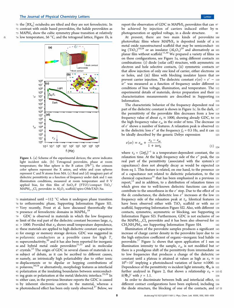
f1 74 low temperature, 56 °C, and the tetragonal lattice, Figure 1b, is
75 maintained until −112 °C when it undergoes phase transition76 to orthorrombic phase, Supporting Information Figure SI1.77 Very recently, Frost et al. have discussed theoretically the78 presence of ferroelectric domains in MAPbI3.
19
79 GDC is observed in materials in which the low frequency80 limit of the real part of the dielectric constant becomes large, ε081 > 1000. Provided that ε0 shows small temperature dependence,82 these materials are applied to high dielectric constant capacitors83 for energy or memory storage devices. GDC was suggested in84 polaronic conductors as a possible cause for high Tc85 superconductivity,20 and it has also been reported for inorganic86 and hybrid metal oxide perovskites21,22 and in molecular87 crystals.23 The origin of GDC in several classes of materials is a88 subject of debate, as it can be ascribed to different causes,89 namely, an intrinsically high polarizability due to either ionic90 displacements or to dipolar or hopping contributions of91 polarons,20,24 or alternatively, morphology features as interfacial92 polarization at the insulating boundaries between semiconduct-93 ing grain or polarization at the metal/dielectric interface.25,26 In94 either case, in the previous literature reports the GDC is caused95 by inherent electronic carriers in the material, whereas a96 photoinduced effect has been only rarely observed.27 Below, we
97report the observation of GDC in MAPbX3 perovskites that can98be achieved by injection of carriers induced either by99photogeneration or applied voltage, in a diode structure.100At present, there are two main kinds of perovskite101photovoltaic films where MAPbX3 is deposited inside of a102metal oxide nanostructured scaffold that may be semiconduct-103ing (TiO2)
10,28 or an insulator (Al2O3)29 and alternatively as
104planar film without scaffold.11,30 We prepared a variety of films105on these configurations, see Figure 1a, using different contacts106combinations: (i) diode (solar cell) structure, with asymmetric107electron and hole selective contacts, (ii) symmetric contacts108that allow injection of only one kind of carrier, either electrons109or holes, and (iii) films with blocking insulator layers that110prevent carrier injection. The dielectric constant ε(ω) = ε′ −111iε″ was measured as a function of frequency under different112conditions of bias voltage, illumination, and temperature. The113experimental details of materials, device preparation and their114characterization measurements are described in Supporting115Information.116The characteristic behavior of the frequency dependent real117part of the dielectric constant is shown in Figure 1c. In the dark,118the permittivity of the perovskite film decreases from a low119frequency value of about ε0 ≈ 1000, showing already GDC, to120the high frequency value ε∞ in the order of tens. The decrease121of ε′ shows a number of features. A relaxation peak is observed122in the dielectric loss ε″ at the frequency fd = 0.5 Hz, and it can123be ideally described by the generic Debye expression
ε ω εε ε
ωτ= +
−+∞
∞
i( )
10
d 124(1)
125where τd = (2πfd)−1 is a temperature-dependent constant, the
126relaxation time. At the high frequency side of the ε″ peak, the127real part of the permittivity (associated with the system’s128capacitance) does not abruptly decay as would be expected129from eq 1. This feature is related, on one hand, to the presence130of a capacitance not related to dielectric polarization, to the131chemical capacitance31 that has been emphasized in a previous132report,13 and in addition, to a distribution of relaxation times133which gives rise to well-known dielectric functions can also134contribute to the smoothness in the ε′ step. Due to the effect of135the dc conductance, the dielectric loss ε″ increases at the low136frequency side of the relaxation peak at τd. Identical features137have been observed either with TiO2 scaffold or with no138scaffold, Supporting Information Figure SI2. Also, with different139contacts, symmetric, asymmetric or blocking, see Supporting140Information Figure SI3. Furthermore, GDC is not exclusive of141the MAPbI3−xClx perovskite and it has been also observed for142CH3NH3PbI3, see Supporting Information Figure SI4.143Illumination of the perovskite samples produces a significant144increase of charge carrier density in the perovskite layer due to145the high extinction coefficient of organic−inorganic lead halide146perovskite.17 Figure 1c shows that upon application of 1 sun147illumination intensity to the sample, ε∞ is not modified but148there is a prodigious shift of the permittivity from intermediate149to low frequencies that produces a change of the dielectric150constant until a plateau is attained at values as high as ε0 ≈151106−107 implying a photoinduced variation of factor ≈1000.152Dependence of the permittivity vs incident light intensity, Φ0, is153 f2further analyzed in Figure 2, that shows a relationship ε0 =154k(Φ0)
γ with γ = 1.1.155In order to discriminate between bulk and interfacial effect,156different contact configurations have been explored, including157 f3the diode structure, the blocking of one of the contacts, and
Figure 1. (a) Scheme of the experimental devices; the arrow indicateslight incident side. (b) Tetragonal perovskite, phase at roomtemperature; the blue sphere is the B cation (Pb2+), the crimsoncolor spheres represent the X anion, and white and cyan spheresrepresent C and N atoms from MA. (c) Real and (d) imaginary part ofdielectric permittivity as a function of frequency under dark and 1 sunillumination conditions, measured at room temperature and 0 Vapplied bias, for thin film of SnO2:F (FTO)/compact TiO2/MAPbI3−xClx perovskite in Al2O3 scaffold/spiro-OMeTAD/Au.
The Journal of Physical Chemistry Letters Letter
dx.doi.org/10.1021/jz5011169 | J. Phys. Chem. Lett. XXXX, XXX, XXX−XXXB

f3 158 symmetric contacts, see Figure 3a and Supporting Information159 Figure SI3. The effect of front contact (illumination side) can160 be appreciated only at high and intermediate frequencies.32
161 However, at low frequency when GDC is observed, ε′ values162 are independent of front contact. A similar trend is observed for163 ε′ when the back contact is modified, see Supporting164 Information Figure SI3. The increase of GDC observed cannot165 be attributed to an effect related with the photocurrent as it is166 also obtained when blocking contacts (20 nm of CaO) are167 inserted in the front or in the back contact. In this sense, the168 independence of the phenomena with the kind of contact169 suggests an intrinsic effect related with bulk perovskite. The170 application of bias voltage at room temperature, from 0 to 1 V,171 with this last value being similar to the photovoltage in the solar172 cell at 1 sun, increases markedly, the ε′ and finally provokes a173 similar GDC effect to that of photogeneration, see Supporting174 Information Figure SI5. These results point to a direct relation175 between the charge carrier density and the increase of the giant176 permittivity, which indistinctly occurs due either to photo-177 generation or to carrier injection by applied bias.178 Voltage and temperature dependence of the GDC effect are179 analyzed in Figure 3b and Supporting Information Figures SI5180 and SI6. At 0 V and low temperature, a relative permittivity of181 ε∞ ≈ 7 is observed at high and intermediate frequencies. This is182 a realistic value for the geometric dielectric permittivity of the183 sample, considering that a value of 7.1 has been recently184 calculated for the CH3NH3PbI3 perovskite.
33 At high T, a richer185 permittivity pattern is obtained, Figure 3b. There is a first step186 at high frequency bringing ε′ to values ∼100 in a thermally187 activated process. This increase of ε′ should be related with a188 capacitance at the contacts.32 At temperature of 273 K and189 higher, see Supporting Information Figure SI6, a second step190 appears that increases real permittivity to 103−104. Finally, a191 third step appears at low frequency promoting real permittivity192 to high GDC of 105−106. Results in Figure 3 confirm that the193 giant dielectric permittivity is related with the increase in carrier194 density due to illumination, charge injection, or temperature.195 Although the dielectric permittivity has been previously studied196 for these perovskite materials, there are no reports of studies197 under illumination or at frequencies as low as the analyzed in198 this paper, and consequently GDC has not been previously
199reported. Nevertheless, previous results of ε′ as high as 200200have been reported for X = (Cl, Br) perovskite single crystals at20150 Hz.34 These values are in the range of the results shown202here.203In summary, the large number of samples investigated, with a204wide variation of internal morphologies, compositions, and205contacts, including samples with insulating contacts, show the206GDC effect in all cases. Therefore, it is reasonable to assume207that the large dielectric constant is an intrinsic effect related to208increased population of electronic carriers and not an interfacial209one.210Already in the dark (without added carriers), the perovskite211shows a very large static dielectric constant. This feature reflects212the response of small dipolar domains to the external electrical213field. The large native dielectric constant could be induced by214structural fluctuations of the perovskite cell, aided by the large215freedom of rotation of the polar CH3NH3
+ cation.32,33 The216dipole−dipole interaction is weak so that the correlation length217ξc of the dipolar domains may comprise only a few unit cells.15
218These domains tend to align to the external field. According to219our observations, when carriers are injected, an enhanced220polarizability is induced by electronic carriers located in the221conduction band and holes in the valence band, corresponding
Figure 2. Plot of the real permittivity as a function of frequency fordifferent incident light intensity (Φ0) from dark to 1 sun, forMAPbI3−xClx perovskite (compact TiO2/ MAPbI3−xClx perovskite inAl2O3 scaffold/spiro-OMeTAD). Measurements have been carried outat room temperature and 0 V applied bias. Inset, linear regression ofdielectric constant vs illumination intensity at f = 50 mHz, observing aclose to linear dependence between ε0 and intensity illumination.
Figure 3. Plots of the real part of dielectric permittivity as a function offrequency. (a) Under dark and 1 sun illumination for thin film ofCH3NH3PbI3−xClx perovskite without scaffold, with spiro-OMeTADas back contact, using different front contacts: TiO2 (diode device);thin CaO ∼20 nm isolating layer (blocking device) and spiro-OMeTAD (symmetric device). Measurements have been carried outat room temperature and 0 V applied bias. (b) At differenttemperatures and three different applied bias conditions for thin filmof perovskite without scaffold and using asymmetric contacts: compactTiO2/CH3NH3PbI3‑xClx/spiro-OMeTAD. Measurements have beencarried out under dark conditions.
The Journal of Physical Chemistry Letters Letter
dx.doi.org/10.1021/jz5011169 | J. Phys. Chem. Lett. XXXX, XXX, XXX−XXXC

222 in the first case to the hybridizations of the 6p orbitals of B223 (lead) and to hybridizations of the 6s orbitals of B and 5p224 orbitals of X (halide) for the valence band.34 However, in a225 highly polar crystal, the electronic carriers become strongly226 localized by electron−phonon coupling. The self-stabilized227 electronic charge in a deformable polar medium is termed a228 polaron, and its slow motion, which drags the lattice distortion,229 is denoted polaron hopping. The presence of excess localized230 charge, with a relative positional freedom to move under231 external or thermal force, modifies the ionic bonding balance of232 the unit cell and causes local distortion. Previous experimental233 results35−38 reveal a high mobility of carriers but those234 measurements are obtained at 109 Hz which is 9 orders of235 magnitude faster than the dynamic polarization observed here.236 Terahertz conductivity only probes the electronic carrier237 dynamics in a very short scale vibrational motion. The238 carrier-induced enhanced polarization is on a very slow scale239 of 1 Hz, as it involves the macroscopic rearrangement of dipolar240 domains, and it will influence the long-range carrier transport.241 Indeed, it can be observed in Supporting Information Figure242 SI2 that the low frequency conductivity decreases by 2 orders243 of magnitude with respect to the intermediate frequency (1244 kHz) conductivity. We remark that long-range transport may245 be either band-like or, in the case of polaron hopping, it will246 involve a small activation energy. It is also likely that different247 mechanisms may coexist in the inhomogeneous environment248 caused by the dipolar domains and grain boundaries structure.249 These facts could have profound implications for the electronic250 and photovoltaic operation of the material that will require a251 detailed investigation. On the other hand, it opens the252 possibility of development of new optoelectronic devices as253 photonic control of memory devices or capacitance based254 photodetectors.
255 ■ ASSOCIATED CONTENT256 *S Supporting Information257 Crystalline structure, methods, dielectric relaxation data. This258 material is available free of charge via the Internet http://pubs.259 acs.org.
260 ■ AUTHOR INFORMATION261 Corresponding Authors262 *I. Mora-Sero. E-mail: [email protected] *J. Bisquert. E-mail: [email protected] Notes265 The authors declare no competing financial interest.
266 ■ ACKNOWLEDGMENTS267 This work was supported by MINECO of Spain under project268 MAT2013-47192-C3-1-R), Universitat Jaume I project269 12I361.01/1, and National Research Foundation of Korea270 (NRF) grant funded by the Korea government (MSIP) (no.271 2008-0061903). We thank SCIC from Universitat Jaume I for272 the help with SEM measurements.
273 ■ REFERENCES(1)274 Park, N.-G. Organometal Perovskite Light Absorbers Toward a
275 20% Efficiency Low-Cost Solid-State Mesoscopic Solar Cell. J. Phys.276 Chem. Lett. 2013, 4, 2423−2429.
(2)277 Snaith, H. J. Perovskites: The Emergence of a New Era for Low-278 Cost, High-Efficiency Solar Cells. J. Phys. Chem. Lett. 2013, 4, 3623−279 3630.
(3) 280Bokov, A. A. Recent Progress in Relaxor Ferroelectrics with281Perovskite Structure. J. Mater. Sci. 2006, 41, 31−52.
(4) 282Zhong, W.; Vanderbilt, D. Competing Structural Instabilities in283Cubic Perovskites. Phys. Rev. Lett. 1995, 74, 2587−2590.
(5) 284Ghita, M.; Fornari, M.; Singh, D. J.; Halilov, S. V. Interplay285Between A-site and B-site Driven Instabilities in Perovskites. Phys. Rev.286B: Condens. Matter Mater. Phys. 2005, 72, 054114.
(6) 287Ohtomo, A.; Muller, D. A.; Grazul, J. L.; Hwang, H. Y. Artificial288Charge-Modulationin Atomic-Scale Perovskite Titanate Superlattices.289Nature 2002, 419, 378−380.
(7) 290Mitzi, D. B. Synthesis, Structure, and Properties of Organic-291Inorganic Perovskites and Related Materials. In Progress in Inorganic292Chemistry; John Wiley & Sons, Inc.: Hoboken, NJ, 2007; pp 1−121.
(8) 293Kojima, A.; Teshima, K.; Shirai, Y.; Miyasaka, T. Organometal294Halide Perovskites as Visible-Light Sensitizers for Photovoltaic Cells. J.295Am. Chem. Soc. 2009, 131, 6050−6051.
(9) 296Im, J.-H.; Lee, C.-R.; Lee, J.-W.; Park, S.-W.; Park, N.-G. 6.5%297Efficient Perovskite Quantum-Dot-Sensitized Solar Cell. Nanoscale2982011, 3, 4088−4093.
(10) 299Burschka, J.; Pellet, N.; Moon, S.-J.; Humphry-Baker, R.; Gao,300P.; Nazeeruddin, M. K.; Gratzel, M. Sequential Deposition as a Route301to High-Performance Perovskite-Sensitized Solar Cells. Nature 2013,302499, 316−319.
(11) 303Liu, M.; Johnston, M. B.; Snaith, H. J. Efficient Planar304Heterojunction Perovskite Solar Cells by Vapour Deposition. Nature3052013, 501, 395−398.
(12) 306Wang, J. T.-W.; Ball, J. M.; Barea, E. M.; Webber, J.-A.; Hunang,307J.; Mora-Sero, I.; Bisquert, J.; Snaith, H. J.; Nicholas, R. J. Low-308temperature processed electron collection layers of Graphene/TiO2
309nanocomposites in thin film perovskite solar cells. Nano Lett. 2014, 14,310724−730.
(13) 311Kim, H.-S.; Mora-Sero, I.; Gonzalez-Pedro, V.; Fabregat-312Santiago, F.; Juarez-Perez, E. J.; Park, N.-G.; Bisquert, J. Mechanism of313Carrier Accumulation in Perovskite Thin-Absorber Solar Cells. Nat.314Commun. 2013, 4, 2242.
(14) 315Gonzalez-Pedro, V.; Juarez-Perez, E. J.; Arsyad, W.-S.; Barea, E.316M.; Fabregat-Santiago, F.; Mora-Sero, I.; Bisquert, J. General Working317Principles of CH3NH3PbX3 Perovskite Solar Cells. Nano Lett. 2014,31814, 888−893.
(15) 319Sanchez, R. S.; Gonzalez-Pedro, V.; Lee, J.-W.; Park, N.-G.;320Kang, Y. S.; Mora-Sero, I.; Bisquert, J. Slow Dynamic Processes in321Lead Halide Perovskite Solar Cells. Characteristic Times and322Hysteresis. J. Phys. Chem. Lett. 2014, DOI: 10.1021/jz5011187.
(16) 323Woodward, P. Octahedral Tilting in Perovskites. II. Structure324Stabilizing Forces. Acta Crystallogr., Sect. B: Struct. Sci. 1997, 53, 44−32566.
(17) 326Stoumpos, C. C.; Malliakas, C. D.; Kanatzidis, M. G.327Semiconducting Tin and Lead Iodide Perovskites with Organic328Cations: Phase Transitions, High Mobilities, and Near-Infrared329Photoluminescent Properties. Inorg. Chem. 2013, 52, 9019−9038.
(18) 330Kim, H.-S.; Im, S. H.; Park, N.-G. Organolead Halide331Perovskite: New Horizons in Solar Cell Research. J. Phys. Chem. C3322014, 118, 5615−5625.
(19) 333Frost, J. M.; Butler, K. T.; Brivio, F.; Hendon, C. H.; van334Schilfgaarde, M.; Walsh, A. Atomistic Origins of High-Performance in335Hybrid Halide Perovskite Solar Cells. Nano Lett. 2014, 14, 2584−3362590.
(20) 337Samara, G. A.; Hammetter, W. F.; Venturini, E. L. Temperature338and Frequency Dependences of the Dielectric Properties of339YBa2Cu3O6+x (x = 0). Phys. Rev. B: Condens. Matter Mater. Phys.3401990, 41, 8974−8980.
(21) 341Ramirez, A. P.; Subramanian, M. A.; Gardel, M.; Blumberg, G.;342Li, D.; Vogt, T.; Shapiro, S. M. Giant Dielectric Constant Response in343a Copper-Titanate. Solid State Commun. 2000, 115, 217−220.
(22) 344Homes, C. C.; Vogt, T.; Shapiro, S. M.; Wakimoto, S.; Ramirez,345A. P. Optical Response of High-Dielectric-Constant Perovskite-346Related Oxide. Science 2001, 293, 673−676.
(23) 347Horiuchi, S.; Kumai, R.; Tokura, Y. Room-Temperature348Ferroelectricity and Gigantic Dielectric Susceptibility on a Supra-
The Journal of Physical Chemistry Letters Letter
dx.doi.org/10.1021/jz5011169 | J. Phys. Chem. Lett. XXXX, XXX, XXX−XXXD
349 molecular Architecture of Phenazine and Deuterated Chloranilic Acid.350 J. Am. Chem. Soc. 2005, 127, 5010−5011.
(24)351 Ligatchev, V. Polaronic Phase Transitions and Complex352 Permittivity of Solid Polar Insulators with Gigantic Dielectric353 Response. Phys. Status Solidi B 2013, 251, 569−592.
(25)354 Lunkenheimer, P.; Bobnar, V.; Pronin, A. V.; Ritus, A. I.;355 Volkov, A. A.; Loidl, A. Origin of Apparent Colossal Dielectric356 Constants. Phys.Rev. B 2002, 66, 052105.
(26)357 Zhang, L.; Tang, Z.-J. Polaron Relaxation and Variable-Range-358 Hopping Conductivity in the Giant-Dielectric-Constant Material359 CaCu3Ti4O12. Phys. Rev. B: Condens. Matter Mater. Phys. 2004, 70,360 174306.
(27)361 Hasegawa, T.; Mouri, S.-I.; Yamada, Y.; Tanaka, K. Giant Photo-362 Induced Dielectricity in SrTiO3. J. Phys. Soc. Jpn. 2003, 72, 41−44.
(28)363 Kim, H.-S.; Lee, C.-R.; Im, J.-H.; Lee, K.-B.; Moehl, T.;364 Marchioro, A.; Moon, S.-J.; Humphry-Baker, R.; Yum, J.-H.; Moser.;365 et al. Lead Iodide Perovskite Sensitized All-Solid-State Submicron366 Thin Film Mesoscopic Solar Cell with Efficiency Exceeding 9%. Sci.367 Rep. 2012, 2, 591.
(29)368 Lee, M. M.; Teuscher, J.; Miyasaka, T.; Murakami, T. N.; Snaith,369 H. J. Efficient Hybrid Solar Cells Based on Meso-Superstructured370 Organometal Halide Perovskites. Science 2012, 338, 643−647.
(30)371 Liu, D.; Kelly, T. L. Perovskite Solar Cells with a Planar372 Heterojunction Structure Prepared Using Room-Temperature Sol-373 ution Processing Techniques. Nat. Photonics 2014, 8, 133−138.
(31)374 Bisquert, J. Chemical Capacitance of Nanostructured Semi-375 conductors: Its Origin and Significance for Heterogeneous Solar Cells.376 Phys. Chem. Chem. Phys. 2003, 5, 5360−5364.
(32)377 Juarez-Perez, E. J.; Wuβler, M.; Fabregat-Santiago, F.; Lakus-378 Wollny, K.; Mankel, E.; Mayer, T.; Jaegermann, W.; Mora-Sero, I. The379 Role of the Selective Contacts in the Performance of Lead Halide380 Perovskite Solar Cells. J. Phys. Chem. Lett. 2014, 5, 680−685.
(33)381 Umari, P.; Mosconi, E.; De Angelis, F. Relativistic GW382 calculations on CH3NH3PbI3 and CH3NH3SnI3 Perovskites for Solar383 Cell Applications. Sci. Rep. 2014, 4, 4467.
(34)384 Maeda, M.; Hattori, M.; Hotta, A.; Suzuki, I. Dielectric Studies385 of CH3NH3PbX3 (X = Cl and Br) Single Crystals. J. Phys. Soc. Jpn.386 1997, 66, 1508−1511.
(35)387 Wasylishen, R. E.; Knop, O.; Macdonald, J. B. Cation Rotation388 in Methylammonium Lead Halides. Solid State Commun. 1985, 56,389 581−582.
(36)390 Mashiyama, H.; Kawamura, Y.; Kubota, Y. The Anti-Polar391 Structure of CH3NH3PbBr3. J. Korean Phys. Soc. 2007, 51, 850−853.
(37)392 Even, J.; Pedesseau, L.; Jancu, J.-M.; Katan, C. Importance of393 Spin−Orbit Coupling in Hybrid Organic/Inorganic Perovskites for394 Photovoltaic Applications. J. Phys. Chem. Lett. 2013, 4, 2999−3005.
(38)395 Wehrenfennig, C.; Eperon, G. E.; Johnston, M. B.; Snaith, H. J.;396 Herz, L. M. High Charge Carrier Mobilities and Lifetimes in397 Organolead Trihalide Perovskites. Adv. Mater. 2014, 26, 1584−1589.
The Journal of Physical Chemistry Letters Letter
dx.doi.org/10.1021/jz5011169 | J. Phys. Chem. Lett. XXXX, XXX, XXX−XXXE