photoemission of semiconductors - philips no. 2 photoemission of semiconductors 55 on a detailed...
TRANSCRIPT

54 PHILlPS TECHNICAL REVIEW VOLUME29
Photoemission of semiconductorsJ. van Laar and J. J. Scheer
The phenomenon of photoemission has played an important role in the history of funda-mental physics. Einstein took the empirical laws underlying photoemission as his startingpoint for postulating, as an extension of Planck' S quantum hypothesis, that light consists ofphotons. Photoemission also has a considerable practical significance; photocathodes areused in many radiation detectors and, in particular, in most image intensifiers. Presentphotocathodes which are reasonably sensitive to visible light, were nearly all evolved moreor less empirically. The article below shows that it is now possible to arrive at a goodphotocathodefor visible light with the aid of more sophisticated methods.
Introduetion
Consider a circuit (fig. 1) consisting of a vacuumtube with two electrodes, cathode-and anode, connectedto a battery and' a sensitive ammeter. The cathode iscold; there is no thermionic emission and thereforeno current flows in the circuit. If the cathode is nowilluminated, the result - under favourable conditions- is a measurable current: the light releases electrons
Fig. I. Principle of photoemission. K cathode, A anode, B battery,Af microammeter. A measurable current flows in the circuit onlywhen the cathode is exposed to light radiation.
from the cathode. This phenomenon, called photo-electric emission or the external photoelectric effect,was first discovered in metals by Elster and Geitel in1850.
This effect was found to obey simple laws whichwere not compatible with the classical wave theory oflight. These laws are easily understood, however, if it isassumed that monochromatic light of frequency p con-sists of a current of light quanta, each with an energyE = hv [ll. An electron inside the cathode has a lowerenergy than in the vacuum outside the cathode. Upon
Drs. J. vall Laar and Dr. J. J. Sc/leer are with Philips ResearchLaboratories, Eindhoven.
absorbing a light quantum [2l, an electron is excited to astate of higher energy. If the energy hp of the absorbedlight quantum is sufficiently high the excited electronis able to surmount the potential barrier at the surface.This picture immediately leads to the rules found by
experiment. 1) No photoemission occurs for photonenergies below a certain value Ed, called the photo-electric work function or long wavelength threshold.2) The number of electrons emitted per second is pro-portional to the number of photons incident per secondon the cathode; in other words, the photoelectric satu-ration current is proportional to the intensity of theincident beam of light. 3) The maximum Emax of theenergy of the emitted electrons is linearly related to thephoton energy: Emax = hv - Ed.It is important in what follows that the emitted
electrons originate from a thin layer at the surface ofthe cathode. Electrons excited at greater depths losetoo much energy on their way to the surface, by inter-action with other electrons and with the atomic lattice,to be able to reach the vacuum. We assume that ofthe electrons excited at a distance x from the surface,only a fraction proportional to exp (-x/d) are emitted,'where d is the "escape depth". Roughly speaking,only the photoelectrons from a surface layer of thick-ness d can escape.In this article we are concerned with photoemission
of semiconductors, and in particular with the researchon this subject which has been done in recent years atthe Philips laboratories in Eindhoven. There are twoaspects of this research: a) The photoelectric effect canbe used as a tool for studying the solid state, in ourcase semiconductor materials. b) As photoemissionfinds wide application in light detectors, an attempt can.be made to design a good light detector using the know-ledge obtained from research under (a). Before entering

1968, No. 2 PHOTOEMISSION OF SEMICONDUCTORS 55
on a detailed exposition of the subject, we should liketo say a little more about these two aspects of theresearch, and also quote a few of the important results.a) In research on semiconductors, photoemission pro-
vides information on the energy levels which have asignificant electron population. The photoelectricwork function gives directly the distance from theupper of these levels to the vacuum level; and becauseof the small escape depth, information is obtained onthe situation at the surface. These are the main pointsof interest in our research. Other investigators [3] havestudied the relative density of states in the occupiedlevels, i.e. the energy band structure, by analysing thewavelength-dependence of the photoemission. Addi-tional information can be obtained along these linesby measuring the energy distribution of the photo-electrons. One might also try to learn something aboutthe escape mechanism of the excited electrons, i.e.about the transfer of energy to the lattice and possiblereflections of electrons at the surface. This is a subjectwhich has so far received relatively little attention.
In addition to the above-mentioned threshold energyfor photoemission, Ed, the thermionic work function cpis a quantity which is directly accessible by experiment,for example by contact potential measurements; cp is thedifference between the vacuum level and the Fermilevel in the semiconductor.According to the band theory of semiconductors a
zone of forbidden energies exists for the electrons inthe material. In general, however, electronic states withenergies in this forbidden zone will occur at the surface(because of impurities, lattice irregularities or otherreasons). These surface states have a considerable in-fluence on the properties of the semiconductor, inparticular on cp and Ba as functions of the dopingCOntent of the semiconductor. As will be shown, theband model leads to the following results for two ex-treme cases:
I) If there are many surface states, all at roughlythe same energy, then cp is independent of the dopingcontent and Ed does depend on it (fig. 2a).2) If there are no surface states, then cp is dependent
upon the doping content and Ed independent of it(fig.2b).In the present article we shall discuss the results of
our work on silicon and gallium arsenide. Our measure-ments show that Si is a typical representative of thefirst case. This situation is so common that the relevantmodel has been assumed to possess general validity.The results of our measurements make it clear, how-ever, that GaAs definitely does not conform to thismodel, but on the contrary shows fairly good agreement'with the second case. [3)
b) If we now attempt to make a good photocathode
N I p N I p
g
Fig. 2. The threshold energy Ed for photoemission and the ther-mionic work function cp as a function of the doping content of asemiconductor, a) in the presence of many surface states at anenergy in the forbidden zone, b) in the absence of surface states.From left to right the doping goes from strong N via weak Nandweak P to strong P; in the centre (I) the semiconductor is in-trinsic.
from a conventional semiconductor, and in particular,a photocathode which is sensitive tö visible light, werequire in the first place that the threshold wavelengthshould lie in the infra-red. In other words, the photo-electric threshold energy must be sufficiently low. Con-ventional semiconductors do not meet this require-ment. There is, however, an empirical method by whichthe photoelectric threshold energy can be shifted to alower energy - the adsorption of metal atoms on thesurface. The most effectivemetal appears to be caesium,which, given the right conditions, makes it possible toreduce the threshold energy to 1.4 eV (which is theionization energy of a caesium atom in the adsorbedstate; 1.4 eV corresponds to 0.90 [J.rnwavelength). Weshall discuss this method, again on the basis of theenergy band model.
Another requirement of a good photocathode is ahigh quantum yield. To achieve this, a substantialfraction of the photons has to be absorbed in the es-cape layer. Heavily-doped GaAs, coated with caesium,looks particularly promising in this repect. In thissystem the energy of an electron in vacuo lies roughlyat the same height as the bottom of the conductionband. This means that an electron, once it has beenexcited to the conduction band, needs hardly any kinet-ic energy to escape from the semiconductor. The escapedepth is then of the order of the diffusion-recombina-tion length, that is to say many times greater than theescape depths normally encountered. These considera-
[1) A. Einstein, Ann. Physik 17, 132, 1905.[2) Itmay be assumed in general that an electron absorbs at the
most one light quantum. Excitation processes in which anelectron absorbs two quanta are also known, but they callfor very special conditions. See H. Sonnenberg, H. Heffnerand W. Spicer, Appl, Phys. Letters 5, 95, 1964. The thresholdenergy for photoemission is then lower by a factor of 2 andthe relation between the numbers of incident photons andemitted electrons is parabolic.D. Brust, Phys, Rev. 139, A 489, 1965; M. L. Cohen andJ. C. Phillips, Phys. Rev. 139, A 912, 1965; N. B. Kindigand W. E. Spicer, Phys. Rev. 138, A 561, 1965.

56 PHILIPS TECHNICAL REVIEW
tions prompted us to make a photocathode ofcaesium-coated GaAs. We found that it gave the quite remark-able yield of about 0.30 electrons per incident photonon the blue side of the visible spectrum.
The first photoemission research on semiconductors,reported twenty years ago, was done with films deposit-ed by vacuum evaporation [41. In order to obtain well-defined materials and surfaces, we confined our ex-periments to vacuum-cleaved single crystals. We shallnot go further into experimental detail here.
VOLUME 29
thermionic work function rp is equal to the thresholdenergy Ed. There are other methods of determining tp,for example contact potential measurements, and theresults can be compared.
Let us now consider an analogous simple model of asemiconductor, shown in fig. 3b. Here, the Fermi levellies in the forbidden zone. The energy band below it(the valence band, with upper edge Ev) is completelyoccupied by electrons, and the band above it (the con-duction band, with lower edge Ec) is empty. In addi-
Fig. 3. Energy bands at the surface of a material. Evac is the potential energy of an electronin vacuo, EF the Fermi level in the material; cp = Evac - El" is the thermionic work function.a) Metal. The threshold for photoemission Eel (long wavelength threshold) is here equal to sp.b) Semiconductor without donors or acceptors at the surface. Ee bottorn of conduction band,Ev top of valence band, Eg = Ee - Ev energy gap. EA = Evac - Ee is the electron affinity.ö = EF - Ev gives the height of the Fermi level with respect to the bands. The threshold forphotoemission is Eu = cp + cl = EA + Eg.c) Semiconductor with surface states s in a narrow energy range. The donors at the surfacegive up electrons to the acceptors in the material. Because of the resultant negative spacecha rge the energy bands are bent.d) Semiconductor with stabilized Fermi level. When an excess of surface donors exists, theygive up their electrons only until the Fermi level coincides with the surface levels. In this casethe Fermi level at the surface is independent ofthe doping content ofthe semiconductor.
Description of photoemission in terms of the band theoryof solids
Using the band theory of solids [5] we shall nowconsider what may be expected in various cases for thephotoernissive threshold energy Ed and the thermionicwork function cp.
We consider first the situation in a metal (fig. 3a).The conduction band - at least at low temperature-is filled with electrons up to the Fermi level EF. All thehigher energy levels are practically empty. At the sur-face between metal and vacuum there is a potentialbarrier: the potential energy of an electron in vacuo(Evac) lies above the Fermi level by an amount cp.Photoemission may be expected from the metal if forthe incident light, h11 ;:?: tp, In a metal, therefore, the
tion to the work function cp = Evac - EF we introducethe electron affinity EA = Evac - Ec, the energy gapEg = Ec - Ev and the quantity 0 = EF - E«, whichdefines the position of the Fermi level in relation to thebands. In photoemission, the electrons originate fromthe valence band [6]; we may therefore expect for thethreshold energy s; = EA + Eg = rp + O.
Let us now consider the effect on Ed and cp of varia-tion of the bulk doping. To a first approximation bulkdoping leaves the position ofthe energy bands unaffect-ed, but it does affect the occupation of the levels andhence the position of the Fermi level; in this way thequantity 0 can be varied between 0 and Eg. Fromfig. 3b it can then be seen at once that cp can be variedbetween EA and EA + Eg by bulk doping, whereas

1968, No. 2 PHOTOEMISSION OF SEMICONDUCTORS 57
Eel = EA + Eg is independent of bulk doping. Forany bulk doping the value of c'J can be determined fromthe bulk properties of the semicond uctor (conductivity,Hall coefficient). Thus, although not so directly as inthe case of a metal, the thermionic work functioncp = Eel - c'J can again be derived from photoemissionmeasurements.
In the model outlined above it was assumed that thesurface causes no complications, in other words that theenergy levels are not dependent upon location withrespect to the surface. Let us consider an energy banddiagram in which the horizontal co-ordinate representsthe spatial co-ordinate perpendicular to the surface.The assumption which we have just mentioned impliesthat in such a ~iiagram the energy bands are representedby straight horizontal lines. It is known, however, thatat the surface of a semicond uctor there is nearly al-ways some bending ofthe energy bands owing to the pres-ence at the surface of additional donors or acceptorswith energy levels in the forbidden zone [71. Suppose,for example, that there exists at the surface of a P-typesemiconductor a large concentration of donor levelssituated in relation to the bands in such a position thatthey would be above the Fermi level if the bands werestraight. Now this is not a state of equilibrium; thedonors at the surface will give up electrons to the accept-ors in the bulk ofthe material, giving rise to a negativespace charge region near the surface combined with apositive surface charge. As a result the potential at thesurface drops and the bands at the surface are bentdownwards (fig. 3e).
The potential distribution at the surface can becalculated by making the assumption that the acceptorlevels in a layer of a given thickness are all filled, andthat the acceptor levels outside that layer are all emp-ty [81. In this layer, the "Schottky layer", there is thus aconstant and finite space charge density, and outsideit a space charge density equal to zero. Solving Pois-son's equation for this charge distribution (in arationalized system) one finds that the potential Vin the layer is parabolically related to the distance xfrom the surface:
V = Ne(x - xo)2/2E,
where N is the concentration of the acceptors, e theelementary charge, E the dielectric constant and Xo the
(4] L. Apker, E. Taft and J. Dickey, Phys. Rev. 74, 1462, 1948.(5] For further details of this model, see L. Heijne, Philips
tech. Rev. 25, 120, 1963/64.(6] This applies to P-type semiconductors and to fairly weakly
doped N-type semiconductors. With very strong N-typedoping some emission from the conduction band is tobe expected. This has never been established with certainty,however.
(7] J. Bardeen, Phys. Rev. 71, 717,1947.(8] See W. Schottky, Z. Physik 118, 539, 1941/42.
thickness of the space charge layer. The total bandbending L1V (the potential difference between surfaceand bulk) is thus
LI V = Nex02/2E. . . . . . . (2)
In other words, for a given total band bending, thespace charge layer is thicker, and the band bendingtherefore more gradual, the lower the bulk doping. Thisis of great importance in what follows.
If the number of surface donors per unit area ofsurface is very large, and if they all lie at roughly thesame energy, then they will give up electrons to theacceptors in the bulk material only until the Fermilevel at the surface just coincides with this donor level(fig. 3d). The Fermi level at the surface, and hence thethermionic work function cp, is therefore independent ofthe doping; in this case we speak of a stabilized Fermilevel. The band bending is now determined by theposition of this donor level at the surface and by theposition of the bands in the bulk of the material inrelation to the Fermi level; the latter position is in turndetermined by the doping.
We now consider the effect of variation of bulk dop-ing on the threshold for photoemission Eel in the case ofa stabilized Fermi level. Figure 4 shows the valenceband at a stabilized Fermi level for P-type doping ofvarious concentrations and for one kind of N-type dop-ing (the conduction band is shown for only one case).
(1)
------------------------~mimlmmlmEv
Fig. 4. Relation between volume doping and valence bandemission when the Fermi level is stabilized. d escape depth. Othersymbols as in fig. 3. J weak P-type doping, 2 stronger, 3 verystrong P-type doping, 4 strong N-type doping. The conductionband is drawn only for case 3. Case 1 corresponds to the "straight-band case" of fig. 3b, Ei! "'" cp + <5. In case 3 the photoelectronsmainly originate from the level Ev "'" EF, so that Ea "'" tp, Incase 4 the threshold is Ei! = cp + <5, but at this threshold energythe yield for photoemission is appreciably smaller than in thestraight-band case (1).

58 PHILlPS TECHNICAL REVIEW VOLUME29
As we have seen, the bending occurs in a thinner layerthe greater the doping concentration. If the doping isvery weak (fig. 4, curve 1) the part of the band ben-ding taking place inside the escape depth d is negligible.In that case the threshold Be is equal to Eg + EA, as itwas with the straight bands in fig. 3b. Stronger P-typedoping lowers the threshold energy Ed, the bands inthe bulk of the material being raised with respect to theenergy of an electron in vacuo. The resulting effect onemission becomes more noticeable as the band bendingoccurs to a greater extent within the escape depth (fig.4,curves 2 and 3). With very strong P-type doping,Ed I'<:::i cp, since the Fermi level in the volume then coin-cides approximately with the upper edge of the valenceband and the thickness of the space charge region issmaller than the escape depth.
Fig. 4, curve 4, shows the valence band for strongN-type doping, with stabilized Fermi level. In thiscase the same threshold is to be expected as withstraight bands, but the yield will be lower for photonenergies close to the threshold.
Table I summarizes the behaviour of 'cp and Ed inboth models when the doping is varied (see also fig.2).
Table I
Model rp=
EA for strongN-type doping;EA + Eg for strongP-type doping
EA + Eg, independ-ent of doping
Straight bands
EA + Eg - a, inde-pendent of doping I EA + Eg for
N-type to weakP-type doping;EA + Eg-a,thus = rp, for strongP-type doping
StabilizedFermi level
In reality, of course, intermediate cases can occurwhere 0 at the surface is neither equal to the value inthe bulk material, as it is in the case of straight bands,
. nor independent of doping, as it is with a stabilizedFermi level.When analysing the results of the measurements one
should bear in mind that the surface levels themselves.can emit photoelectrons, which may mask in particularthe weak beginning of the valence band emission. Forthis reason N-type material is generally less suitablefor research on valence band emission, since theemission is exceptionally low near the threshold in thismaterial.
Experimental results for silicon
With reference to the foregoing model, we shall nowdiscuss the results of our measurements on single crys-tals of silicon [9]. We beginwith.the spectral distribution
of the emission in the case of weakly doped materials,i.e. both P-type and N-type containing 1016 chargecarriers per cmê (fig.5). We see in the first place thatthe spectral distribution is the same for both P-type andN-type material, indicating that the doping in each casemust be weak enough to allow us to consider the bandsas straight (the space charge layer being very muchgreater than the escape depth for photoelectrons).
f
o P_Si(I016Ga/cm3)x N-Si(1016P/cm3)
25
20
15
10
5
Fig. 5. Yield y of the photoemission for P-type and N-type silicon(I X 1016 charge carrlers/cmê) as a function of photon energy hv,The solid curve represents the relation y = 42(hv - 5.4)3/2. Thescale for y is arbitrary.
Secondly, we see that the curve consists oftwo parts,i.e. a "tail" with a very low yield followed by a steeplyrising part beginning at 5.4 eV. We interpret the tailas emission from surface levels. In the following weshall put forward two arguments in support of this.The steep section of the curve is attributed to the va-lence band emission. The threshold energy for this emis-sion is thus 5.4 eV. This part of the curve appears to
[9] J. van Laar and J. J. Scheer, Philips Res. Repts.17, 101, 1962,and Rep. Int. Conf. on the Physics of Semiconductors,Exeter 1962, p. 827 (pub!. Inst. Phys./Phys. Soc., London1962).
[10] G. W. Gobeli and F. G. Allen, Phys. Rev. 127, 141, 1962.[11] The values of rp - 4.85 eV for weakly doped and 4.90 eV
for strongly doped P-type material - indicate that the stabi-Iization of the Fermi level is not complete.
1968, No. 2 PHOTOEMISSION OF SEMICONDUCTORS
be well described by the purely empirical expressiony oc (hv - 5.4)3/2, where hv is the energy of thephotons in electron volts.Let us now consider the emission from more strongly
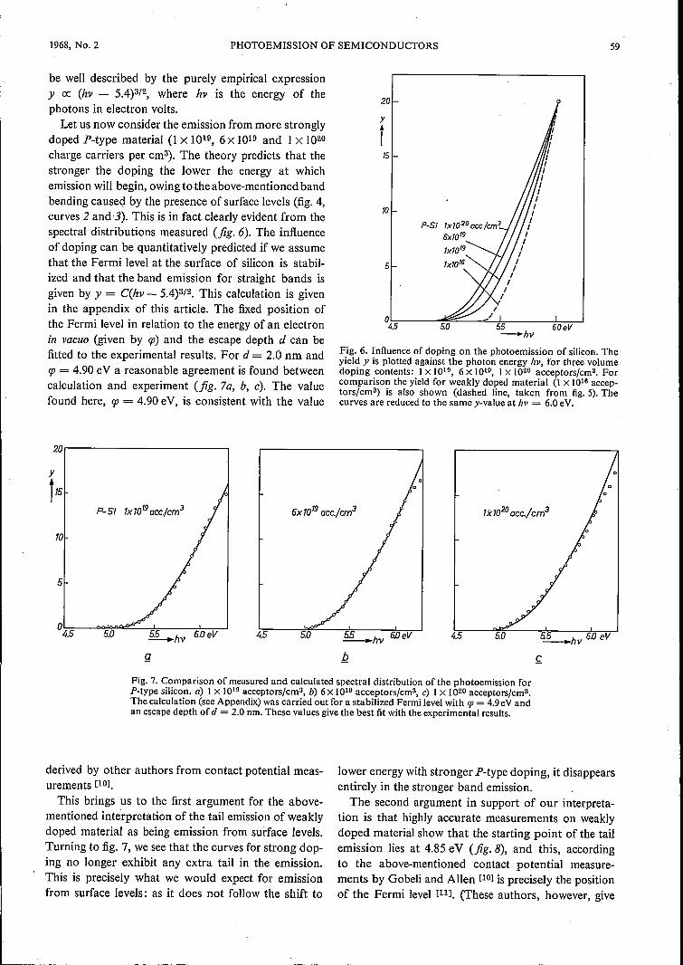
doped P-type material (1 X 10¹⁹, 6 X 10¹⁹ and 1X 10²⁰charge carriers per cmê). The theory predicts that thestronger the doping the lower the energy at whichemission will begin, owing to the above-mentioned bandbending caused by the presence of surface levels (fig. 4,curves 2 and·3). This is in fact clearly evident from thespectral distributions measured (fig. 6). The influenceof doping can be quantitatively predicted if we assumethat the Fermi level at the surface of silicon is stabil-ized and that the band emission for straight bands isgiven by y = Cth» - 5.4)3/2. This calculation is givenin the appendix of this article. The fixed position ofthe Fermi level in relation to the energy of an electronin vacuo (given by cp) and the escape depth d can befitted to the experimental results. For d = 2.0 nm andcp = 4.90 eVa reasonable agreement is found betweencalculation and experiment (fig. 7a, b, c). The valuefound here, cp = 4.90 eV, is consistent with the value
20.----------------------,
to
P-Si fx1019 acc./cm3
5
5.0 6.0eV
g
Fig. 6. Influence of doping on the photoemission of silicon. Theyield y is plotted against the photon energy hv, for three volumedoping contents: 1X 10¹⁹, 6 X 10¹⁹, IX 1020 acceptors/ems. Forcomparison the yield for weakly doped material (I X 1016 accep-tors/erne) is also shown (dashed line, taken from fig. 5). Thecurves are reduced to the same y-value at /ZV = 6.0 eV.
4.5 5.0 ~hy 6.0eV
12.
4.5 ~hv 6.0eV
£
Fig. 7. Comparison of measured and calculated spectral distribution of the photoemission forP-type silicon. a) I X 1019 acceptors/ems, b) 6x 10¹⁹ acceptors/cmê, c) I X 1020 acceptors/cmê,The calculation (see Appendix) was carried out for a stabilized Fermi level with cp =4.9 eV andan escape depth of d = 2.0 nm. These values give the best fit with the experimental results.
derived by other authors from contact potential meas-urements [lOl.
This brings us to the first argument for the above-mentioned interpretation of the tail emission of weaklydoped material as being emission from surface levels.Turning to fig. 7, we see that the curves for strong dop-ing no longer exhibit any extra tail in the emission.This is precisely what we would expect for emissionfrom surface levels: as it does not follow the shift to
lower energy with stronger P-type doping, it disappearsentirely in the stronger band emission.The second argument in support of our interpreta-
tion is that highly accurate measurements on weaklydoped material show that the starting point of the tailemission lies at 4.85 eV (fig.8), and this, accordingto the above-mentioned contact potential measure-ments by Gobeli and Allen [lOl is precisely the positionof the Fermi level [Ill. (These authors, however, give
59

60 PHILIPS TECHNICAL REVIEW VOLUME 29
30'r-~======~-----'--~o
25Y
to
i5
10
5
Fig. 8. Photoemission of silicon with weak P-type doping(1.6 X 10¹⁶ Ga/cmê): the yield y as a function of photon energyhv. In the inset, y2/5 is plotted against hv, The solid curve repre-sents the relation
y = Uw - 4.85)5/2 + 28.3(hv - 5.36)3/2.
The tail emission (hv < 5.4'eV) is attributed to emission fromsurface levels.
a different interpretation of the tail emission.) This partof the emission appears to satisfy the empirical ex-pression y cc (kv - 4.85)5/2. Summarizing, the entirespectral distribution for weakly doped material istherefore given by:
y = Cl(hv - 4.85)5/2 + Co(hv - 5.4)3/2,
where CO/Cl is found to be approximately equal to 30.The photoemis.sion of silicon can therefore be de-
scribed by assuming that the Fermi level at the surfaceis stabilized at 4.9 eV below vacuum and that EA hasthe value 5.4 -1.1 = 4.3 eV (Eg = 1.1 eV). Thus, atthesurface, the Fermi level lies 0.6 eVbelow the bottomofthe conduction band.This stabilization of the Fermi level occurs for P-type
volume doping up to 1020 cm-3• Using equation (2)we can calculate the number of filled acceptors perunit surface of the space charge layer. Taking N =1020 cm-3, .1V = 0.5 volt, e = eoer, er = 11.8, eo =8.9 X 10⁻¹² F/m and e = 1.6X 10⁻¹⁹ C, we find thisnumber to be Nx« = (2.1VeNle)1/2 ~ 1013 cm-2• Tosupply this charge theremust be at least 1013 surfacelevels per cm~.These levels must be localized within an
energy region of 0.1 eV, as follows from the accuracywith which the stabilization of the Fermi level wasdetermined.
The 5/2power law found for the emission from sur-face levelsproves to be quite common, also in caseswherethe surface levels are due to impurities [121. The 5/2exponent was found, for example, for the tail emissionof cadmium telluride surfaces with impurities due tocleavage in air or baking in vacuo. The tail emissionhere must definitely be attributed to the impurities,because a clean surface, obtained by vacuum cleavagedoes not give this emission [131.
Experimental results for gallium arsenide
In the case of silicon we found a very nearly stabilizedFermi level at the surface. Our results for galliumarsenide [141 clearly show that the Fermi level here isnot stabilized and that the situation in fact conformsfairly well to the simple straight-band model (seefig.3b).
The first indication of the lack of surface levels is thespectral distribution of the photoemission from weaklydoped P-type material (fig. 9). The greater part ofthis distribution can be dèscribed by the empirical re-lation y o: (kv - 5.57)3/2, and only a small additionaltail occurs at low photon energies. In the case of siliconthe 3/2 power was characteristic of valence-band emis-sion. If this applies to gallium arsenide too, the smalltail emission means that the surface levels are presentonly in a low concentration, so that there may well beno stabilization of the Fermi level here. This is in factclearly evident from the very limited influence of bulkdoping on the photoemission (fig. 10).
For a stabilized Fermi level this influence can becalculated as in the case of silicon. Assuming that theescape depth in GaAs is also 2.0 nm, we have made thecalculation for two positions of the Fermi level, givenrespectively by (j = 0.1 ev and (j = 0.7 eV at the sur-face. From figs. 11 and 12 'it appears that the firstchoice gives only a poor fit with the experimental re-sults and that the second does not fit at all. We con-clude therefore that the Fermi level is not stabilized ..
This conclusion is confirmed by the results ofmeas-urements of the effect of bulk doping on the thermi-onic work function cp. To obtain information on thispoint, contact potential measurements were carried outto determine the difference in cp between N-type andP-type material [141. The results of these experimentsshowed that, even in the case of weakly doped material,the difference in cp roughly corresponded to the differ-
[12] J. 'J. Scheer and J. van Laar, Physics Letters 3, 246, 1963.[13] J. J. Scheer and J. van Laar, Philips Res. Repts.16, 323, 1961.[14] J. van Laar and J. J. Scheer, Surface Sci. 8, 342, 1967.[15] W. E. Spicer, J. appl. Phys, 31, 2077, 1960.

1968, No. 2 PHOTOEMISSION OF SEMICONDUCTORS 61
r
o
ence in the position of the Fermi level in the volume.This ties up with the assumption that the bands runmore or less straight at the surface.
Photocathodes for visible light; lowering of the workfunction by adsorption
We shall now deal at somewhat greater length withthe problem, mentioned in the introduction, of makinga satisfactory photocathode for visible light. First, itshould be stated that good photocathodes in use at thepresent time can have a very high maximum yield, withvalues up to 0.30 (expressed in electrons per incidentphoton). A yield as high as this can scarcely be im-proved upon. The Na2KSb-Cs photocathode [15] hasits threshold wavelength at 0.85 Il-m; this is a sufficientlylong wavelength for the detection of visible light. Exist-ing cathodes therefore meet the requirements forvisible-light detectors reasonably well.
All the good photocathodes were evolved more orless empirically. Later it turned out that all efficientcathodes were P-type semiconductors. The questionthat now arises is whether more scientific methodscould be applied to the development of photocathodes,using known semiconductors.A high yield can only be obtained with valence band
emission. In the example of silicon given above, thethreshold for photoemission with strong P-type doping
Fig. 9. Photoemission of GaAs with weak P-type doping(2.5 X 10¹⁷ acceptors/cm"). The 2/3 power of the yield y is givenas a function of photon energy hv, The tail emission is of littlesignificance.
o
y y y
ÎN-GaAs
ÎN-GaAs
ÎP-GaAs
ZOx 10'8 don./cm3 ZOx10'8don./cm3 4.ox1O'9acc.fcm3
P-GaAs2.5x10'7 acc';cm3 6=0.7eV O=0.7eV
5.4 5.8 6.0 6.2 6.4eV_hv
Fig. 10. Influence of volume dopingon the photoemission of GaAs.The yield y is given as a function ofphoton energy hv for P-type ma-terial, 4.0 X 10¹⁹ acceptors/cm" and2.5 X 1017 acceptors/ern" and forN-type, 1.0 X 10¹⁸ donors/cm". Thècurves have been reduced to thesame y-value at hv = 6.35 eV.
Fig. 11. The yield y as a function ofhv for N-GaAs,l X 1018 donors/cm",as found 'theoretically for two val-ues of 0 and an escape depth d of2.0 nm. The experimental points(squares) are the same as in fig.10. The curves have again beenreduced to the same y-value athv = 6.35 eV.
5.8 6.0 6.2 6.4 eV_hv
Fig. 12. As fig. 11, but now .forP-GaAs, 4 X 10¹⁹ acceptors/cmê.Only a few of the corresponding ex-perimental points of fig. 10 areshown (the circles). The zero pointof the theoretical curve (i.e. thethreshold energy Ed) for 0 = 0.7 eVis at EA + Eg - 0 = 5.57 - 0.7 =4.87 eV.

62 PHILl PS TECHNICAL REVIEW
was 4.9 eV, that is to say in the far ultraviolet (0.25 um).In the case of GaAs it is not possible to shift the emis-sion to lower energy by means of band bending, andEd here is even higher (5.6 eV). Values as high as thisare found with most semiconductors.
As we mentioned in the introduction, however, amethod does exist by which the threshold for photo-emission can be shifted to a lower energy, i.e. by theadsorption of electropositive metal atoms on the surfaceof the semiconductor. We shall now consider thismethod.
Q
VOLUME 29
charge. The negative space charge causes band bend-ing: the potential inside the semiconductor rises in re-lation to the vacuum level. Upon the further adsorp-tion of atoms the band bending increases. This processcontinues until the Fermi level has risen to a level slight-ly above the bottom of the cond uction band at thesurface (fig. l3b). As soon as this has happened, theelectrons of the adsorbed atoms enter the conductionband, in which the number of available states is verylarge; there is no further increase ofthe space charge andtherefore no further band bending. The metal ions, to-
-------EF
d
Fig. 13. Lowering of the threshold energy for photoernission by the adsorption of metalatoms. a) If the ionization energy la,)s of an adsorbed metal atom is lower than the work func-tion of the clean surface of P-type material, the metal atoms give up electrons to the acceptorsin the bulk. This gives rise to band bending, which continues until the Fermi level coincideswith the bottom of the conduction band at the surface (b). Upon further adsorption the donat-ed electrons enter the conduction band. They form together with the positive metal ions a di-pole layer, as a result of which the levels in the semiconductor are raised with respect to thevacuum level. This continues until the optimum situation c is reached, where cp = lads, InN-type material (d) there is virtually no band bending; almost right from the beginning a di-pole layer is formed in this material by the positive metal atoms and the donated electrons inthe conduction band.
Suppose we have a P-type semiconductor whose Fer-mi level at the surface is not stabilized (see fig. 13).Metal atoms are now adsorbed on this surface (fig. 13a).Let the ionization energy of these atoms in the ad-sorbed state be fads (this need not be equal to theionization energy of the free atom). If lads is smallerthan the thermionic work function cp of the semicon-ductor, the metal atoms will give up an electron to theacceptors in the bulk of the semiconductor. As a re-sult, a negative space charge arises in the semiconduc-tor, and the metal ions form an opposite surface
gether with the electrons in the conduction band, form adipole layer at the surface. These electrons can be re-garded as the image charge of the ions: the surface hasnow acquired a metallic character. The Fermi levelrises with respect to the vacuum level as a result of theincreasing potential drop across the dipole layer. Thiscontinues until the Fermi level coincides with the donorlevel of the adsorbed atom (lads below vacuum level).In this situation cp = fads (fig. 13c). Upon further ad-sorption the semiconductor accepts no more electrons.
Since the electrons are able to tunnel through the

1968, No. 2 PHOTOEMISSION OF SEM[CONDUCTORS 63
potential barrier of the dipole layer, the thresholdenergy for photoemission Ee finally falls to lads instrongly P-type doped material. In material with weakP-type doping, after adsorption of metal atoms,("straight bands") the threshold energy is Ed = lads +Eg, as in N-type material, in which hardly any bandbending occurs (fig. 13d).
We shall now examine what happens when metalatoms are adsorbed on a semiconductor surface witha stabilized Fermi level (fig. 14). If lads is sufficientlylow, the metal atoms will give up their electron to the
Q
Fig. 14. Adsorption of metal on a P-type semiconductor withstabilized Fermi level. If the ionization energy [ads of an adsorbedatom is lower than the work function t:p of the semiconductorwithout metal (see a), the metal atoms give up electrons to thesurface levels. The dipole layer formed raises the levels in thesemiconductor with respect to the vacuumlevel. In the optimumsituation (b), tp is again equal to lads,
surface states at the Fermi level (fig. l4a). The adsorbedions now form together with the resultant negative sur-face charge a dipole layer which causes the potentialin the semiconductor to rise with respect to vacuum.As adsorption continues a maximum lowering of thethreshold is reached when the Fermi level has risen tolads below vacuum level (fig. 14b). Thereafter the ad-sorbed atoms have no further reason to give up anelectron. In this situation the thermionic work func-tion is again cp = lads, For weakly doped material thelong wavelength threshold is now Ed = lad + O. Forstrong P-type doping we again find Ed f'>j lads,
[16] J. J. Scheer and J. van Laar, Solid State Comm. 5, 303, 1967.
The behaviour of some semiconductors is not entirely inaccordance with this model. If the surface of these materials isclean, the Fermi level is not stabilized, but the surface, upon ad-sorbing metal atoms, behaves as if the Fermi level were in factstabilized. In this case the adsorption of foreign atoms evidentlygives rise to excess surface levels. Gallium arsenide is a typicalexample of such a semiconductor [16]. No satisfactory explanationhas yet been found for this phenomenon.
If one is looking for a photocathode with a lowthreshold energy, the above considerations show thatone should take a strongly P-type doped semiconduc-tor and cover it with metal atoms for which lads issmall; whether or not the Fermi level is stabilized isthen immaterial as far as the threshold energy is con-cerned, this being equal to lads,
The lowest value of lads is found for caesium, atabout 1.4 eV (0.90 fLm wavelength), virtually inde-pendent of the substrate.
For P-type silicon coated with Cs this value hasin fact been found as the threshold for valence bandemission [91. By varying the volume doping it is possibleto estimate the escape depth for electrons in the rele-vant energy region. The result is d f'>j 20 nm, a valuealso found for practical photocathodes [151.
The yield of P-type silicon with Cs is very low, how-ever « 1%). This is due to the fact that the electrontransitions in silicon, caused by light with a photonenergy equal to or slightly higher than 1.4 eV, areindirect transitions. These are transitions betweenstates of different momentum, the electron exchangingmomentum with the lattice vibrations. In a diagramgiving the energy E against momentum k (see fig. 15)these are represented by an oblique arrow. The yield islow with indirect transitions for two reasons:
E
f
a b
-k
Fig. IS. Energy E as a function of momentum (k) for electronsin a semiconductor. C is the conduction band, Vthe valenceband.a is a direct transition, b an indirect transition.

r-----:,--------~------------------------------------------.--~~~--~-
64 PHILlPS TECHNICAL REVIEW VOLUME29
1) The transition probability is very small for an indi-rect transition. This is the opposite to the case of adirect transition, where the momentum is preserved, sothat no lattice vibrations are needed to maintain thebalance of momentum. Because of this the absorptionof the relevant light is weak and only a small fractionof the light is absorbed in the escape layer, In siliconthe penetration depth is roughly 1 [Lm,which is verymuch greater than the escape depth found of 20 nm.Thus, the majority ofthe electrons excited do notreachthe surface, and therefore do not contribute to thephotoemission.2) Even the light that is absorbed in the escape layeris to a great extent ineffective, for in principle, at a givenhv, an electron can go from any state in the valenceband to any state in the conduction band, provided theenergy difference agrees. In a large percentage of thesetransitions the final state of the electron is a state in theconduction band below Evac (see fig. 16). These areknown as competing transitions.
_k
Fig. 16. Indirect transitions in silicon with strong P-type doping(EF lies at the top of the valence band), coated with Cs (cp =Evac-EF = 1.4 eV), ais a transition where the electron receivesan energy higher than Evac; this electron may be emitted; bandc, competing transitions where the excited electron cannot beemitted. The energy difference:./iv,;:'för ai' band c is the same,and greater than Ed = 1.4 eV.
This being said, it is obviously of interest to consid-er semiconductors in which the relevant transitions aredirect ones. The disadvantage mentioned under item(2) is then not encountered, for at a given /ZV there isgenerally only one set of states in the valence and con-duction bands possessing the same momentum; thereare no competing (direct) transitions. As far as item (1)is concerned, with direct transitions stronger lightabsorption is usually found, because the probabilityof a direct transition is so much greater than for anindirect transition. On the other hand it could well be
that the number of possible indirect transitions ismuch greater than the number of possible direct ones.
Let us confine ourselves to the simple situation inwhich the extremes of the two bands lie at the same kvalue. We again consider semiconductors with strongP-type doping, so that EF coincides with the top of thevalence band, and which are coated with Cs, so thatEvac - EF = cp = 1.4 eV. Fig.17 shows three cases:a) Eg> cp, b) Eg = cp, c) Eg < cp. Case (a) is unfa-vourable since the electron must first enter the conduc-tion band before it can be emitted; the threshold forphotoemission is thus Ed = Eg > cp. Again, in case(c) the threshold for direct transitions is shifted towardsthe blue, because the point where Evac intersects theconduction band corresponds to a valence band levelbelow EF. Only in case (b) is Ed not greater than butequal to cp. It follows, then, that we should choosesemiconductors in which the energy gap relevant to di-rect transitions, i.e. the optical energy gap, is roughlyequal to 1.4 eV. (It mayalso be deduced from fig.I7cthat, at a given Eg < cp, the value of E« approachescloser to cp as the valence band becomes flatter and theconduction band sharper, in other words as the effec-tive mass of the holes in the valence band becomesgreater and that of the electrons in the conduction bandsmaller.)
Semiconductors whose energy gap does not differtoowidely from 1.4 eV are CdTe (Eg = 1.5 eV), GaAs(Eg = 1.35eV) and InP (Eg = 1.29 eV). CdTe isimmediately ruled out because it cannot be given thenecessary high P-type doping content. The hope thatthe absorption of the light might be stronger than forsilicon, since direct transitions are involved, is not ful-filled by the other two materials; the penetration depthfor light with /ZV values greater than Eg is of the order of1 [Lm,as in silicon.This penetration depth is much too great as long as
we are concerned with escape depths of 20 nm. Thisdoes not however apply to the cases of fig. 17a and b.In these cases the bottom of the conduction band inthe bulk is above the vacuum level (fig. 17a) or coin-cides with it (fig.17b). This means that electrons in theconduction band possessing thermal energy are al-ready capable of escaping into the vacuum. In otherwords, excited electrons can still be emitted after theyhave entirely lost their kinetic energy by collisions inthe conduction band. Here, then, the escape depth is nolonger determined by the mean free path of high-energy electrons but by the diffusion-recombinationlength. This lies roughly between 0.1 and 1 [Lm.In thesecases, therefore, a penetration depth of 1 [Lmfor lightis very reasonable. GaAs is a material that closelyapproximates to the situation in fig. 17b.These considerations led us to make an experimental

1968, No. 2 PHOTOEMISSION OF SEMICONDUCTORS 65
photocathode of GaAs, coated with Cs, which gaves~rprisingly good results. Single crystals of GaAs wereused, with 3x 10¹⁹ acceptors/ems, cleaved in vacuo [17].
The measured spectral distribution (fig. 18) shows thatthe threshold for photoemission is 1.35 eV (0.90 fl.m),which is near the expected value. On the blue side ofthe visible spectrum (0.4 fl.m) the yield is about 0.30electrons per incident photon; at 3.5 eV (0.35 fl.m) it
g
rises to as much as 0.35. After correction for reflectedlight, a yield is found of roughly 0.50 electrons perabsorbed quantum, which is the maximum that can beexpected (since half the excited electrons go away fromthe surface and into the bulk of the materia!). Thesensitivity to light with a colour temperature of2850 OK is 500 fl.A/lm. This photocathode is thereforeeven better than the Na2KSb-Cs cathode, which has a
Eg
Fig. 17. P-doped semiconductors with a simple band structure, with the same value of q;(given by the deposited metal) but with different optical energy gap Eg. a) Eg > tp, b) Eg = q;,c) Eg < tp. Only in case (b) is the threshold for direct transitions equal to tp ; both in (a) and (c)the threshold Ed is greater than tp,
long wavelength threshold of 0.82 fl.m and a sensitivityof 300 fl.A/lm.
Appendix: Calculation of the effect of bulk doping on the photo-emission of silicon
We take a P-type semiconductor and choose a co-ordinatesystem in which the x-axis is perpendicular to the surface of thesemiconductor; x = 0 at the surface, and x > 0 in the bulk.
We make the following assumptions:1) The escape probability of an electron excited at a distance xfrom the surface has the form exp(-xfd), the escape depth dbeing independent of the energy of the excited electron.2) The intensity of the light at a distance x from the surface isgiven by 10 exp (-xfm), the penetration depth m being indepen-dent of the photon energy.3) The photoemission of a crystal with straight bands is given byy = Cth» - Eo)3/2, as we found empirically.
The contribution Lly to the photoemission originating from' alayer of thickness zlx at a distance x from the surface is givenfor straight bands by:
Lly(x) = A(hv - EO)3/2 e-X/L zlx,
Fig. 18. Spectral distribution of 11, the yield per photon, of the whereL-I = d-I + m-I and A is an arbitrary constant.photoemission of P-type GaAs (3 x 10¹⁹ acceptorsjcmê) coatedwith Cs. The solid curve gives the yield in electrons per incidentphoton, the dashed curve the yield in electrons eper absorbedphoton. [17] J. J. Scheer and J. van Laar, Solid State Comm. 3, 189, 1965.

66 PHILlPS TECHNICAL REVIEW VOLUME29
Suppose now, that as a result of band bending the valenceband at position x is shifted to higher energy by an amountoE(x) with respect to its position at the surface. We now make theadditional assumption that the contribution to the photoemissionis independent of the state in the conduction band occupied bythe excited electron. We then have for bent bands:
Lly(x) = A {hv + oE(x) - Eo}3/2 e-:r:/L LI~. • • • (3)
According to eqs. (1) and (2), for a Schottky layer:
oE(x) = e{V(xo) - Vex)} = LIE {I -:-(x-:-oxon,
where LIE = eLl V is the total band bending. Substitution of (4)in (3) and integration with respect to x gives:
xo
f [ { (X- XO)2}]3/2y(hv) = A hv - Eo + LIE 1 - -x;;- e-:r:/L dx +o
+ AL(hv - Eo + LlE)3/2 e-:r:o/L •
(4)
The last term in this equation originates from the part of thecrystal outside the space charge region.
The value of the integral for a given xo, LIE and L has to bedetermined numerically.
Summary. The article discusses a study made of the surfaceproperties of semiconductors by investigating their photo-emission. The spectral distribution of the photoemission wasmeasured on vacuum-cleaved single crystals of silicon and galliumarsenide with various amounts of P-type and N-type doping.The results are interpreted in terms of the band theory of solids,where the bands can be bent at the surface by a space charge dueto surface states and where, in the presence of excess surfacestates, the Fermi level may be stabilized in the surface levels. Theemitted electrons come from a surface layer of thickness d, theescape depth. In weakly doped silicon the main emission comesfrom the valence band and "tail emission" from the surface states.In Si the Fermi level is stabilized; with increasing impurity con-tent, thelayer where band bending occurs finally becomes thinnerthan the escape depth; this explains the observed change in thespectral distribution of the emission. In the case of GaAs it is
concluded that there are virtually no surface levels, no band bend-ing and no stabilization of the Fermi level. For photoemissionin the visible region the threshold energy of nearly all semi-conductors is too high ('" 5 eV); it can be lowered by the adsorp-tion of metal atoms, e.g. of Cs (to 1.4 eV). The yield of P-Sicoated with Cs is small due to a) a too small absorption coefficientand b) "competing transitions" that do not result in emission.Strongly P-doped GaAs coated with Cs may be expected to be agood photoemitter in the visible region since the competingtransitions are of little significanee and the escape depth is un-usually large owing to the vacuum level and the bottom of theconduction band being coincident. This has been confirmed byexperiment. An experimental photocathode of this compositionhas a long wavelength threshold at 0.9 !Lmand an outstandingphotoemmission: the yield is 0.35 electrons per incident photonat 0.35 !Lm.

1968, No. 2 67
Recent scientific publicationsThese publications are contributed by staff of laboratories and 'plants which formpart. of or co-operate with enterprises of the Philips group of companies, particularlyby staff of the following research laboratories:
Philips Research Laboratories, Eindhoven, Netherlands EMullard Research Laboratories, Redhill (Surrey), England MLaboratoires d'Electronique et de Physique Appliquée, Limeil-Brévannes(S.O.), France L
PhilipsZentrallaboratorium GmbH, Aachenlaboratory, Weisshausstrasse,51 Aachen, Germany A
Philips Zentrallaboratorium GmbH, Hamburg laboratory, Vogt-Kölln-Strasse 30, 2 Hamburg-Stellingen, Germany H
MBLE Laboratoire de Recherche, 2 avenue Van Becelaere, Brussels 17(Boitsfort), Belgium. B
Reprints of most of these publications will be available in the near future. Requestsfor reprints should be addressed to the respective laboratories (see the code letter) orto Philips Research Laboratories, Eindhoven, Netherlands.
G. A. Acket: Determination of the Hall mobility of hotelectrons in gallium arsenide using 8 mm microwaves.Physics Letters 25A, 374-376, 1967 (No. 5). E
L. K.H. van Beek, J. Helfferich, H. Jonker & Th. P. G.W. Thijssens: Properties of diazosulfonates, Part Ir.The rate of the reaction between 2-methoxybenzene-diazonium and sulfite ions;L. K. H. van Beek, J. Helfferich, H. J. Houtman & H.Jonker: idem, Part lIL The absorption spectra ofp-substituted-benzene-trans-diazosulfonates; Part IV.The absorption spectra of 0- and m-substituted ben-zenediazosulfonates.Rec. Trav. chim. Pays-Bas 86, 749-754, 975-980, 981-985, 1967 (Nos. 8, 10). E
G. Blasse & A. Bril: A new phosphor for flying-spotcathode-ray tubes for color television: yellow-emittingy3Al501Z-Ce3+.Appl. Phys. Letters 11, 53·55, 1967 (No. 2). E
G. Blasse & A. Bril: Structure and Eu3+-fluorescenceof lithium and sodium lanthanide silicates and germa-nates.J. inorg. nucl. Chem. 29, 2231-2241, 1967 (No. 9). E
G. Blasse & A. Bril: Investigations of Tb3+-activatedphosphors.Philips Res. Repts. 22, 481-504, 1967 (No. 5). E
P. Blume & A. Stecker: Physikalische Eigenschaftenvon Lochstreifenpapier, I, I1, lILFeinwerktechnik 71, 262-271, 325-334, 518-527, 1967(Nos. 6, 7, 11). H
A. J. van Bommel & F. Meyer: A low energy electrondiffraction study of the PH3 adsorption on the Si (111)surface.Surface Sci. 8, 381-398, 1967 (No. 4). E
A. J. van Bommel & F. Meyer: LEED study of a nickelinduced surface structure on silicon (111).Surface Sci. 8,467-472, 1967 (No. 4). E
J. C. Brice: Diffusive and kinetic processes in growthfrom solution.J. Crystal Growth 1, 161-163, 1967(No. 3). M
A. Broese van Groenou: Permeability of some oxidesand metals at low temperatures.J. appl. Phys. 38, 3317-3320, 1967 (No. 8). E
A. Broese van Groenou: Magnetic after-effects in high-amplitude fields.Philips Res. Repts. 22, 463-480, 1967(No. 5). E, M
K. H. J. Buschow & J. H. N. van Vucht: Comments on"The aluminium-rich parts of the Al-Sm and Al-Dysystems".J. less-common Met. 13, 369-370, 1967(No. 3). E
H. B. G. Casimir: Van der Waals-Wechselwirkungen.Naturwiss. 54,435-438, 1967 (No. 15/16). E
A. Claassen & L. Bastings: The determination of alu-minium with 8-hydroxyquinoline, Part I. Precipitationin acetate-buffered solution;A. Claassen, L. Bastings & J. Visser: idem, Part II.Precipitation in ammoniacal cyanide-EDTA solution.Analyst 92,614-617,618-621, 1967 (No. 1099). E
J. B. Davies: Propagation in rectangular waveguidefilled with skew uniaxial dielectric.IEEE Trans. MTT-15, 372-376, 1967(No. 6). M
H: Dormont, J. Frey, J. Salmon & M. Valton: Contri-bution à l'établissement d'une nouvelle équation ciné-tique.C. R. Acad. Sci. Paris 264A, 978-980,1967 (No. 22). L

68 PHILlPS TECHNICAL REVIEW VOLUME29
W. F. Druyvesteyn: The resistivity of hard supercon-ductors subjected to an increasing field.Physics Letters 25A, 31-32, 1967 (No. I). E
P. Eckerlin, A. Rabenau & H. Nortmann: Zur Kenntnisdes Systems Be3N2-SbN4, Ill. Darstellung und Eigen-schaften von BeSiN2;P. Eckerlin: idem, IV. Die Kristallstruktur von BeSiN2.Z. anorg. allgem. Chemie 353, 113-121, 225-235, 1967(Nos. 3/4, 5/6). A
J. Flinn, G. Bew & F. Berz: Low frequency noise inMOS field effect transistors.Solid-State Electronics 10, 833-845, 1967 (No. 8). M
L. Fraiture & J. Neirynck: Optimum elliptic-functionfilters for distributed constant systems.IEEE Trans. MTI-15, 482-483, 1967 (No. 8). B
A. H. Gomes de Mesquita: Refinement of the crystalstructure of SiC type 6H.Acta cryst. 23,610-617, 1967 (No. 4). E
A. H. Gomes de Mesquita: The crystal structure of2,2' -diaminodiphenyl disulphide.Acta cryst. 23, 671-672, 1967 (No. 4). E
G. E. G. Hardeman, G. B. Gerritsen & R. P. van Sta-pele: Effect of random crystal fields on the electron-nuclear double-resonance spectrum of cobalt-dopedZnSe.Phys. Rev. 160, 281-286, 1967 (No. 2). E
E. Himmelbauer & J. C. Francken: On the sensitivityof oscilloscope tubes.Philips Res. Repts. 22, 515-540, 1967 (No. 5).
F. M. Klaassen: High-frequency noise of the junctionfield-effect transistor.IEEE Trans. ED-14, 368-373, 1967 (No. 7). E
F. M. Klaassen & J. Prins: Thermal noise of MOS tran-sistors.Philips Res. Repts. 22, 505-514, 1967 (No. 5). E
G. Klein & H. Koelmans : Active thin film devices.Festkörperprobleme 7, 183-199, 1967. E
E. Kooi: The surface properties of thermally oxidizedsilicon.Festkörperprobleme 7, 132-157, 1967. E
W. Kwestroo & P. H. G. M. Vromans: Preparation ofthree modifications of pure tin (IT) oxide.J. inorg. nuel. Chem. 29, 2187-2190, 1967 (No. 9). E
J. van Laar & J. J. Scheer: Influence of volume dopeon Fermi level position at gallium arsenide surfaces.Surface Sci. 8, 342-356, 1967 (No. 3). E
A. J. Lambell: Experimental information-storage filter.Proc. Instn. Electr. Engrs. 114, 1185-1192, 1967(No. 9).. M
H. de Lang & G. Bouwhuis: Measurements on theanomalous non-linear preference for circular modepolarization in a 1.523 (L He-Ne laser.Physics Letters 25A, 406-407, 1967 (No. 5). E
B. Lersmacher, H. Lydtin & W. F. Knippenberg: ZurTechnologie der pyrolytischen Graphit-Herstellung.Chemie-Ing-Technik 39,833-842,1967 (No. 14). A, E
F. E. Maranzana: Contributions to the theory of theanomalous Hall effect in ferro- and antiferromagneticmaterials.Phys. Rev. 160, 421-429, 1967 (No. 2). E
P. Massini & G. Voorn: The effect of ferredoxin andferrous ion on the chlorophyll sensitized photoreduc-tion of dinitrophenol.Photochem. Photobiol. 6,851-856, 1967 (No. 11). E
R. Memming & G. Schwandt: Potential and chargedistribution at semiconductor-electrolyte interfaces.Angew. Chemie: Int. Edit. in English 6,851-861, 1967(No. 10); German Edit. 79,833-844,1967 (No. 19). H
J.-P. Morel: Etude par l'effet Mössbauer de l'aiman-tation spontanée des deux sous-réseaux de, fer dans leferrite NiFe204.J. Phys. Chem. Solids 28, 629-634, 1967 (No. 4). E
W. C. Nieuwpoort & G. Blasse: Het ionogene bindings-model.Chem. Weekblad 63, 497-501, 1967 (No. 44). E
J. M. Noothoven van Goor: Hall coefficients of telluri-um-doped bismuth.Physics Letters 25A, 442-443, 1967 (No. 6). E
A. van Oostrom: Adsorption of nitrogen on single-crystal faces of tungsten.J. chem. Phys. 47, 761-769, 1967 (No. 2). E
A. van Oostrom: Totaldruckmessung nach dem Ioni-sationsprinzip und ihre Störeffekte.Vakuum-Technik 16, 159-167, 1967 (No. 7). E
F. A. Staas, A. K. Niessen & W. F. Druyvesteyn: Someexperiments on the distribution of a transport currentin sheets of superconductors of the second kind.Philips Res. Repts. 22,445-462, 1967 (No. 5). E
W. L. Wanmaker & D. Radielovié: Luminescentie vanfosfaten.Chem. Weekblad 63, 486-494, 1967 (No. 43).
J. te Winkel & B. C. Bourna: An investigation intotransistor cross-modulation at VHF under AGC con-ditions.IEEE Trans. ED-14, 374-381, 1967 (No. 7). E
H. J. de Wit & C. Crevecoeur: n-type Hall effect inMnO.Physics Letters 25A, 393-394, 1967 (No. 5). E
L. E. Zegers: The reduction of systematic jitter in atransmission chain with digital regenerators.IEEE Trans. COM-15, 542-551, 1967 (No. 4). E
Volume 29, 1968, No. 2 Published 14th Februarypages 37-68