photodiode response - thorlabs saturation and noise floor •the saturation limit of a photodiode is...
TRANSCRIPT

Photodiode Saturation and Noise Floor
• The saturation limit of a photodiode is dependent on the reverse bias voltage and the load resistance.
• The noise floor of a photodiode detection system depends not only on the NEP of the diode but also significantly on the load resistance.
• The location of the noise floor and the saturation limit determine the linear region of the photodiode response.
Page 1/12
0 2 4 6 8 100
1
2
3
4
5
6Photodiode Response
Ou
tpu
t V
olt
ag
e (
V)
Incident Power (mW)
Saturation Limit
1E-6 1E-5 1E-4 1E-3 0.011E-8
1E-7
1E-6
1E-5
Outp
ut V
oltage (
V)
Incident Power (mW)
Noise Floor
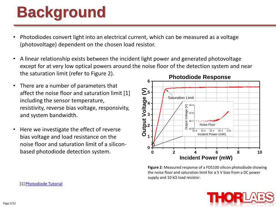
Figure 1: Measured silicon photodiode FDS100 response showing the noise floor and saturation limit for a 5 V bias and 10 kΩ load resistor.
Background
• Photodiodes convert light into an electrical current, which can be measured as a voltage (photovoltage) dependent on the chosen load resistor.
• A linear relationship exists between the incident light power and generated photovoltage except for at very low optical powers around the noise floor of the detection system and near the saturation limit (refer to Figure 2).
[1] Photodiode Tutorial
• There are a number of parameters that affect the noise floor and saturation limit [1] including the sensor temperature, resistivity, reverse bias voltage, responsivity, and system bandwidth.
• Here we investigate the effect of reverse bias voltage and load resistance on the noise floor and saturation limit of a silicon-based photodiode detection system.
Page 2/12
Figure 2: Measured response of a FDS100 silicon photodiode showing the noise floor and saturation limit for a 5 V bias from a DC power supply and 10 kΩ load resistor.
0 2 4 6 8 100
1
2
3
4
5
6Photodiode Response
Ou
tpu
t V
olt
ag
e (
V)
Incident Power (mW)
Saturation Limit
1E-6 1E-5 1E-4 1E-3 0.011E-8
1E-7
1E-6
1E-5
Outp
ut V
oltage (
V)
Incident Power (mW)
Noise Floor
Theoretical Considerations: Noise Floor
• The typical way to define the minimum detectable power of a detector is by a measure of the noise equivalent power (NEP) given in units of W/HZ1/2.
• NEP is caused mostly by shot noise from the statistical nature of photons and has been defined as the optical power necessary to provide an output signal equal to the detector noise. In other words, it is the power incident upon the detector that yields a signal-to-noise ratio (SNR) of 1. [2,3]
• As an example, the NEP for the FDS100 under a 20 V bias is 1.2 x 10⁻¹⁴ W/HZ1/2, when illuminated at 900 nm. Assuming a typical sillicon responsivity of 0.57 A/W at 900 nm and a bandwidth of 1 Hz, the calculated photovoltage noise would be approximately 0.3 pV with a 50 Ω load, when using Ohm’s Law (V = I·R).
• It is important to note that another measure of minimum detectable power is the D*, which normalizes the inverse of the NEP to a 1 cm2 detector area and a 1 Hz bandwidth. [2,3]
• Johnson noise is caused by the thermal motion of charged particles in a resistive element:
• As an example, the Johnson noise of a 50 Ω resistor at 25˚C and 1 Hz bandwidth is VRMS = 9071.4 pV, when using the temperature conversion: T(K) = T(˚C) + 273.15.
• We can see from the two examples that the thermal noise (Johnson noise) from a resistive load is typically much larger than the inherent NEP for low bandwidth applications (<192 Hz for our example parameters), so we typically say the noise floor of the system is Johnson-noise limited for continuous wave lasers.
kB: Boltzmann’s Constant (1.38x10⁻²³ J/K)T: Temperature (K)B: System Bandwidth (Hz) R: Load Resistance (Ω)
Eq. 1
[2] A. Daniels, Field Guide to Infrared Systems, Detectors, and FPAs, 2nd Edition, SPIE Press, Bellingham, Washington USA, 2007. [3] Verena Mackowiak, et al., NEP – Noise Equivalent Power. Thorlabs Inc., 2015[4] J. Liu, Photonic Devices. Cambridge University Press, Cambridge, UK, 2005.
𝑉𝑅𝑀𝑆 = 4𝑘𝐵𝑇𝐵𝑅
Page 3/12
• Saturation occurs when no additional photocurrent outputs from the photodiode as the incident optical power increases.
• Photodiodes saturate when the output photovoltage approaches the reverse bias voltage. Since photodiodes output a current, the saturation limit can be adjusted by modifying the reverse bias voltage (within specification) or reducing the load resistance.
• The photovoltage response is linear according to Eq 2 above the noise floor (discussed on the previous page) and prior to the bias voltage (Vbias). If the incident optical power Ps increases to a point where the photovoltage Vout ≈ Vbias, the output is considered saturated. [5]
Theoretical Considerations: Saturation
Page 4/12
I0: Dark Current ℛ: Photodiode Responsivity Ps: Input Optical Power
𝑉𝑜𝑢𝑡 = 𝐼𝑜 + ℛ𝑃𝑠 𝑅 Eq. 2
[5] R.S. Quimby, Photonics and Lasers: An Introduction, John Wiley & Sons, 2006.[6] Hamamatsu’s Si Photodiode Handbook
• It is important to note that the maximum output voltage can be larger than Vbias based on the built-in voltage of the photodiode on the order of hundreds of mV and the photodiode serial resistance on the order of single Ω [6]:
Vbi: built-in voltageRS: photodiode resistance𝑃𝑠𝑎𝑡 =
𝑉𝑏𝑖𝑎𝑠 + 𝑉𝑏𝑖(𝑅𝑆 + 𝑅)ℛ
Eq. 3
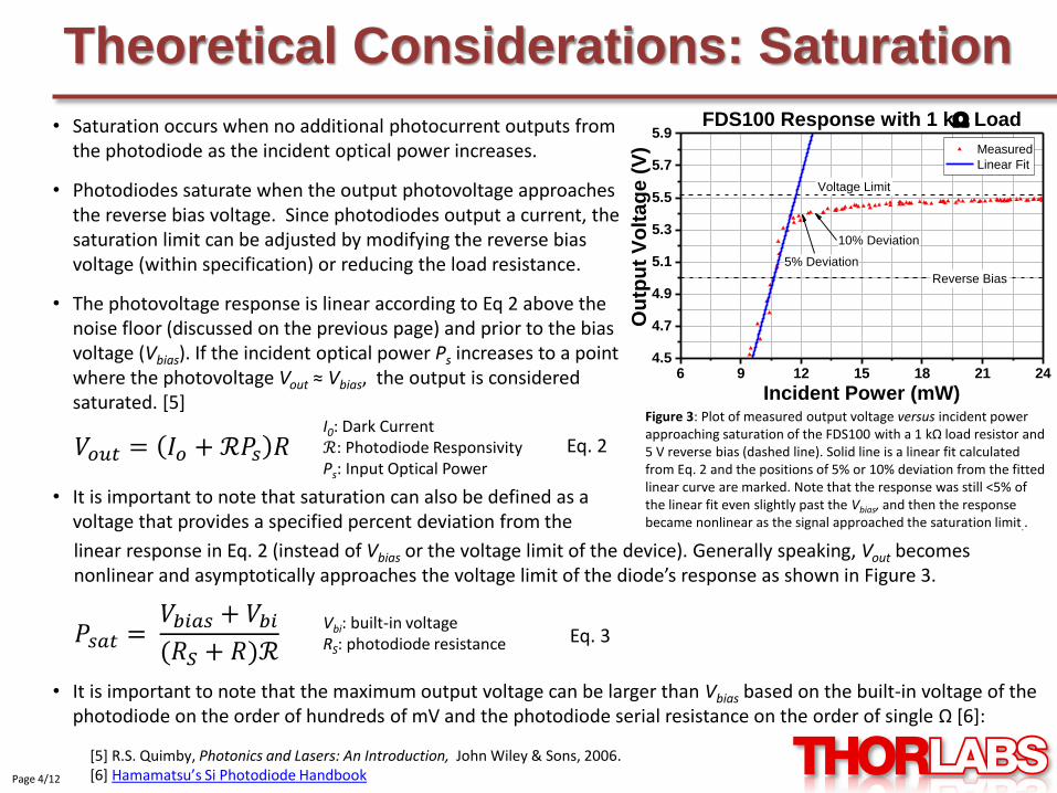
Figure 3: Plot of measured output voltage versus incident power approaching saturation of the FDS100 with a 1 kΩ load resistor and 5 V reverse bias (dashed line). Solid line is a linear fit calculated from Eq. 2 and the positions of 5% or 10% deviation from the fitted linear curve are marked. Note that the response was still <5% of the linear fit even slightly past the Vbias, and then the response became nonlinear as the signal approached the saturation limit..
• It is important to note that saturation can also be defined as a voltage that provides a specified percent deviation from the
linear response in Eq. 2 (instead of Vbias or the voltage limit of the device). Generally speaking, Vout becomes nonlinear and asymptotically approaches the voltage limit of the diode’s response as shown in Figure 3.
6 9 12 15 18 21 244.5
4.7
4.9
5.1
5.3
5.5
5.7
5.9
Voltage Limit
10% Deviation
Measured
Linear Fit
FDS100 Response with 1 k Load
Ou
tpu
t V
olt
ag
e (
V)
Incident Power (mW)
5% Deviation
Reverse Bias
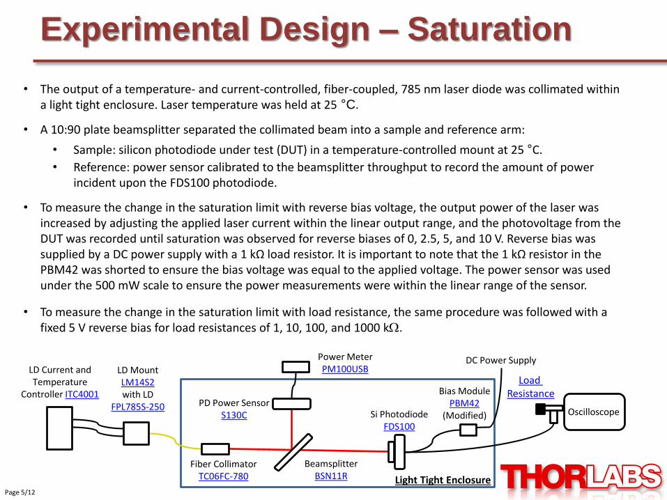
Experimental Design – Saturation
• The output of a temperature- and current-controlled, fiber-coupled, 785 nm laser diode was collimated within a light tight enclosure. Laser temperature was held at 25 °C.
• A 10:90 plate beamsplitter separated the collimated beam into a sample and reference arm:
• Sample: silicon photodiode under test (DUT) in a temperature-controlled mount at 25 °C.
• Reference: power sensor calibrated to the beamsplitter throughput to record the amount of power incident upon the FDS100 photodiode.
• To measure the change in the saturation limit with reverse bias voltage, the output power of the laser was increased by adjusting the applied laser current within the linear output range, and the photovoltage from the DUT was recorded until saturation was observed for reverse biases of 0, 2.5, 5, and 10 V. Reverse bias was supplied by a DC power supply with a 1 kΩ load resistor. It is important to note that the 1 kΩ resistor in the PBM42 was shorted to ensure the bias voltage was equal to the applied voltage. The power sensor was used under the 500 mW scale to ensure the power measurements were within the linear range of the sensor.
• To measure the change in the saturation limit with load resistance, the same procedure was followed with a fixed 5 V reverse bias for load resistances of 1, 10, 100, and 1000 k.
Fiber CollimatorTC06FC-780
BeamsplitterBSN11R
PD Power SensorS130C
Power MeterPM100USB
Load Resistance
Light Tight Enclosure
Oscilloscope
LD MountLM14S2with LD
FPL785S-250
LD Current and Temperature
Controller ITC4001
Si PhotodiodeFDS100
Bias ModulePBM42
(Modified)
Page 5/12
DC Power Supply
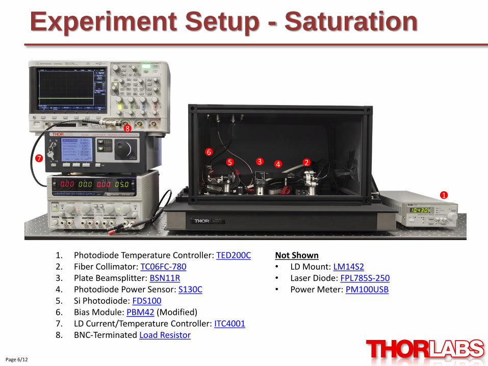
Experiment Setup - Saturation
23 45
67
8
Not Shown• LD Mount: LM14S2• Laser Diode: FPL785S-250• Power Meter: PM100USB
1. Photodiode Temperature Controller: TED200C2. Fiber Collimator: TC06FC-7803. Plate Beamsplitter: BSN11R4. Photodiode Power Sensor: S130C5. Si Photodiode: FDS1006. Bias Module: PBM42 (Modified)7. LD Current/Temperature Controller: ITC40018. BNC-Terminated Load Resistor
Page 6/12
1
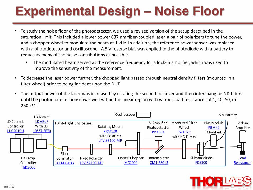
Experimental Design – Noise Floor
• To study the noise floor of the photodetector, we used a revised version of the setup described in the saturation limit. This included a lower power 637 nm fiber-coupled laser, a pair of polarizers to tune the power, and a chopper wheel to modulate the beam at 1 kHz. In addition, the reference power sensor was replaced with a photodetector and oscilloscope. A 5 V reverse bias was applied to the photodiode with a battery to reduce as many of the noise contributions as possible.
• The modulated beam served as the reference frequency for a lock-in amplifier, which was used to improve the sensitivity of the measurement.
• To decrease the laser power further, the chopped light passed through neutral density filters (mounted in a filter wheel) prior to being incident upon the DUT.
• The output power of the laser was increased by rotating the second polarizer and then interchanging ND filters until the photodiode response was well within the linear region with various load resistances of 1, 10, 50, or 250 k.
Rotating MountPRM1Z8
with PolarizerLPVISB100-MP
BeamsplitterCM1-BS013
Si PhotodiodeFDS100
Si Amplified Photodetector
PDA36A
Oscilloscope
Lock-in Amplifier
Light-Tight Enclosure
Optical ChopperMC2000
Motorized Filter Wheel
FW102Cwith ND Filters
Bias ModulePBM42
(Modified)
LoadResistance
FiberCollimator
TC06FC-633
LD Temp ControllerTED200C
LD MountLDM9LPWith LD
LP637-SF70
LD Current ControllerLDC201CU
Fixed PolarizerLPVISA100-MP
Page 7/12
5 V Battery
Experiment Setup – Noise Floor
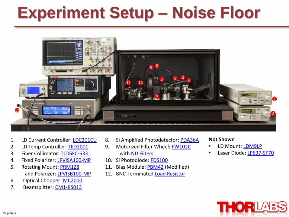
1. LD Current Controller: LDC201CU2. LD Temp Controller: TED200C3. Fiber Collimator: TC06FC-6334. Fixed Polarizer: LPVISA100-MP5. Rotating Mount: PRM1Z8
and Polarizer: LPVISB100-MP6. Optical Chopper: MC20007. Beamsplitter: CM1-BS013
8. Si Amplified Photodetector: PDA36A9. Motorized Filter Wheel: FW102C
with ND Filters10. Si Photodiode: FDS10011. Bias Module: PBM42 (Modified)12. BNC-Terminated Load Resistor
Not Shown• LD Mount: LDM9LP• Laser Diode: LP637-SF70
Page 8/12
1
435
2
6
7
89
1011
12
Results – Noise Floor
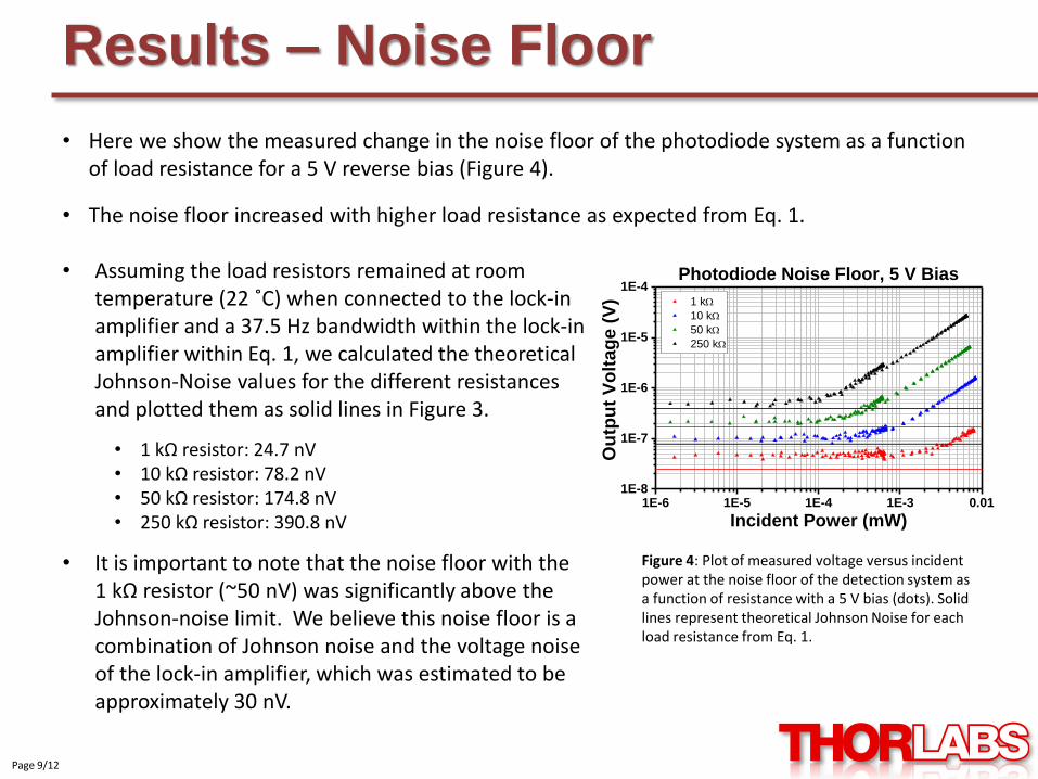
• Here we show the measured change in the noise floor of the photodiode system as a function of load resistance for a 5 V reverse bias (Figure 4).
• The noise floor increased with higher load resistance as expected from Eq. 1.
Page 9/12
Figure 4: Plot of measured voltage versus incident power at the noise floor of the detection system as a function of resistance with a 5 V bias (dots). Solid lines represent theoretical Johnson Noise for each load resistance from Eq. 1.
1E-6 1E-5 1E-4 1E-3 0.011E-8
1E-7
1E-6
1E-5
1E-4 1 k
10 k
50 k
250 k
Photodiode Noise Floor, 5 V Bias
Ou
tpu
t V
olt
ag
e (
V)
Incident Power (mW)
• Assuming the load resistors remained at room temperature (22 ˚C) when connected to the lock-in amplifier and a 37.5 Hz bandwidth within the lock-in amplifier within Eq. 1, we calculated the theoretical Johnson-Noise values for the different resistances and plotted them as solid lines in Figure 3.
• 1 kΩ resistor: 24.7 nV• 10 kΩ resistor: 78.2 nV• 50 kΩ resistor: 174.8 nV• 250 kΩ resistor: 390.8 nV
• It is important to note that the noise floor with the 1 kΩ resistor (~50 nV) was significantly above the Johnson-noise limit. We believe this noise floor is a combination of Johnson noise and the voltage noise of the lock-in amplifier, which was estimated to be approximately 30 nV.
Results - Saturation
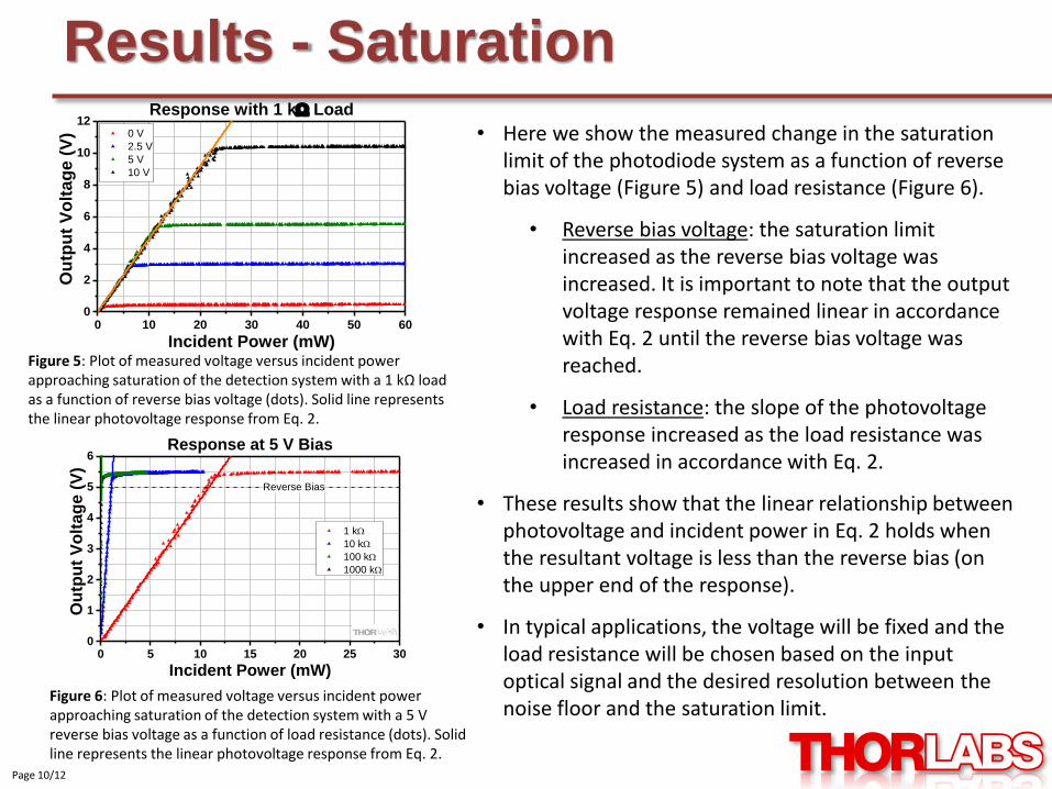
• Here we show the measured change in the saturation limit of the photodiode system as a function of reverse bias voltage (Figure 5) and load resistance (Figure 6).
• Reverse bias voltage: the saturation limit increased as the reverse bias voltage was increased. It is important to note that the output voltage response remained linear in accordance with Eq. 2 until the reverse bias voltage was reached.
• Load resistance: the slope of the photovoltage response increased as the load resistance was increased in accordance with Eq. 2.
• These results show that the linear relationship between photovoltage and incident power in Eq. 2 holds when the resultant voltage is less than the reverse bias (on the upper end of the response).
• In typical applications, the voltage will be fixed and the load resistance will be chosen based on the input optical signal and the desired resolution between the noise floor and the saturation limit.
Page 10/12
Figure 5: Plot of measured voltage versus incident power approaching saturation of the detection system with a 1 kΩ load as a function of reverse bias voltage (dots). Solid line represents the linear photovoltage response from Eq. 2.
Figure 6: Plot of measured voltage versus incident power approaching saturation of the detection system with a 5 V reverse bias voltage as a function of load resistance (dots). Solid line represents the linear photovoltage response from Eq. 2.
0 10 20 30 40 50 600
2
4
6
8
10
12 0 V
2.5 V
5 V
10 V
Response with 1 k Load
Ou
tpu
t V
olt
ag
e (
V)
Incident Power (mW)
0 5 10 15 20 25 300
1
2
3
4
5
6
1 k
10 k
100 k
1000 k
Response at 5 V Bias
Ou
tpu
t V
olt
ag
e (
V)
Incident Power (mW)
Reverse Bias
Experimental Limitations
• Only a single silicon photodiode (FDS100) was examined to demonstrate the general effects of reverse bias voltage and load resistance, but we expect similar behavior for other wavelengths and detector materials according to Eqs. 1 and 2.
• Noise floor measurements were limited by the sensitivity and noise floor of the Signal Recovery 7265 lock-in amplifier (~30 nV noise at our measured bandwidth of 37.5 Hz). This played a larger role when other noise contributions were small, such as the 1 kΩ resistance results on page 9.
• For simplicity, we have assumed an uniformly distributed beam incident upon the photodiode and the photodiode’s responsivity was uniform over the beam area. In our experiments, we filled 50%-80% of the detector’s active area. As the beam is relatively large, the saturation will be caused by the overall power, not the power density.
• We have also assumed that the photodiode responsivity was stable over the measurement time. The detectors were measured at normal incidence to the optical axis, and we assume the detector surfaces were isotropic. We have also ignored polarization effects with regard to the responsivity. [7]
• For the purposes of these measurements, the photodiode was occasionally operated beyond the maximum reverse current specification. For normal use, it is not recommended to exceed this value.
• The results discussed here were obtained using a low noise CW laser source and may not be accurate for pulsed applications.
Page 11/12
[7] T.C Larason and J.M. Houston, “Spectroradiometric Detector Measurements: Ultraviolet, Visible, and Near-Infrared Detectors for Spectral Power”, NIST Special Publication 250-41 (2008)
Summary
• We have demonstrated the reverse bias voltage and load resistor dependence on the location of the noise floor and saturation limit for a silicon photodiode.
• Increasing the reverse bias voltage provided a higher saturation limit.
• Decreasing the load resistance decreased the overall noise floor and increased the saturation limit. Decreasing the load resistance also decreased the slope of the photovoltage response.
• During our measurements the FDS100 photodiode voltage response remained linear (approximately within 5%) through the bias voltage and then became highly non-linear. From these results, we assume the saturation point, or maximum valid voltage that should be measured is the bias voltage.
• It is important to emphasize that the specified maximum reverse bias voltage and reverse current limits should not be exceeded during continual use.
• In low bandwidth applications with a small load and no cooling, the noise floor is Johnson noise-limited by the load resistor. NEP specifications for most photodiodes address the intrinsic shot noise of the photodiode, so it is essential to consider the Johnson noise of resistive elements in the circuit when estimating the effective noise floor.
• There are many noise sources for a photodiode detection system such as Johnson noise from the load resistor, shot noise from the incident light, and voltage noise from the measuring instrument. The dominant noise sources are dependent on the system configuration.
Page 12/12