photocurrent measurements pellinger
TRANSCRIPT
Photocurrent measurementtechniques
____________________________________________________________________________________________________________________
Photocurrent measurement techniques (Nanosystems I - Seminar - 1.12.08 @ WSI) [email protected]
____________________________________________________________________________________________________________________
Photocurrent measurement techniques (Nanosystems I - Seminar - 1.12.08 @ WSI) [email protected]
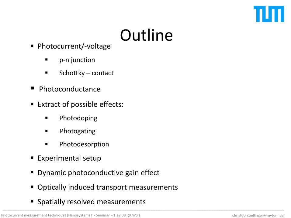
Outline Photocurrent/-voltage
p-n junction
Schottky – contact
Photoconductance
Extract of possible effects:
Photodoping
Photogating
Photodesorption
Experimental setup
Dynamic photoconductive gain effect
Optically induced transport measurements
Spatially resolved measurements
____________________________________________________________________________________________________________________
Photocurrent measurement techniques (Nanosystems I - Seminar - 1.12.08 @ WSI) [email protected]
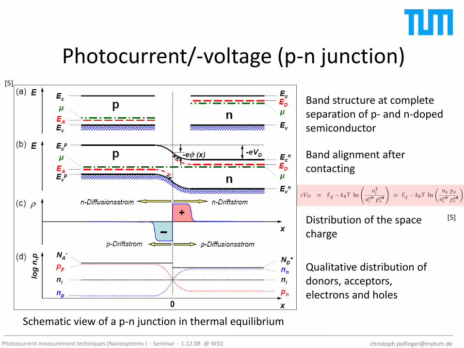
Band alignment after contacting
Distribution of the space charge
Qualitative distribution of donors, acceptors, electrons and holes
Photocurrent/-voltage (p-n junction)
Band structure at complete separation of p- and n-doped semiconductor
Schematic view of a p-n junction in thermal equilibrium
[5]
[5]
____________________________________________________________________________________________________________________
Photocurrent measurement techniques (Nanosystems I - Seminar - 1.12.08 @ WSI) [email protected]
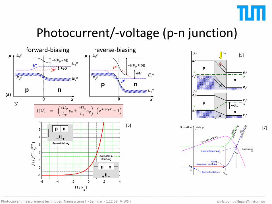
Photocurrent/-voltage (p-n junction)reverse-biasingforward-biasing
[7]
[5]
[5]
[5]
____________________________________________________________________________________________________________________
Photocurrent measurement techniques (Nanosystems I - Seminar - 1.12.08 @ WSI) [email protected]
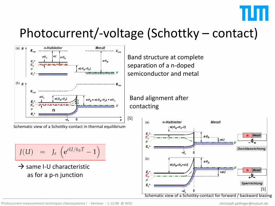
Photocurrent/-voltage (Schottky – contact)
Band alignment after contacting
Schematic view of a Schottky-contact in thermal equilibrium
Band structure at complete separation of a n-doped semiconductor and metal
[5]
[5]
same I-U characteristic as for a p-n junction
Schematic view of a Schottky-contact for forward / backward biasing
____________________________________________________________________________________________________________________
Photocurrent measurement techniques (Nanosystems I - Seminar - 1.12.08 @ WSI) [email protected]
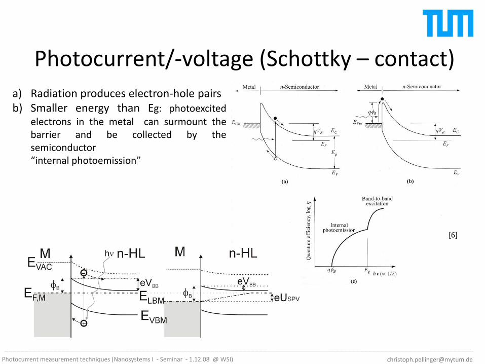
Photocurrent/-voltage (Schottky – contact)
[6]
a) Radiation produces electron-hole pairsb) Smaller energy than Eg: photoexcited
electrons in the metal can surmount thebarrier and be collected by thesemiconductor“internal photoemission”
____________________________________________________________________________________________________________________
Photocurrent measurement techniques (Nanosystems I - Seminar - 1.12.08 @ WSI) [email protected]
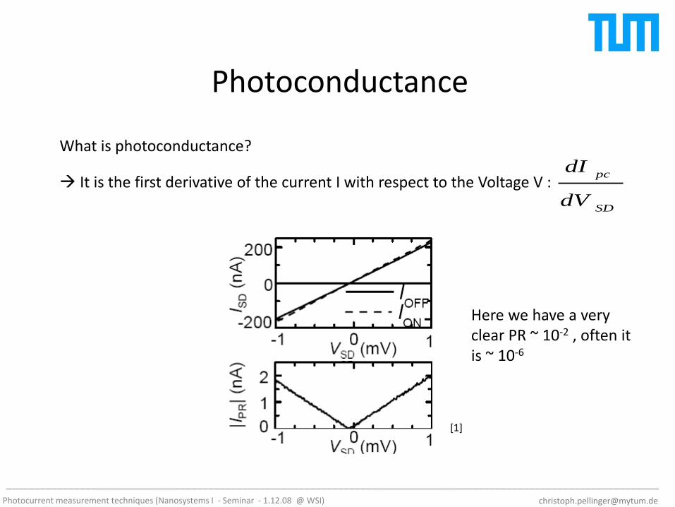
Photoconductance
What is photoconductance?
SD
pc
dV
dI It is the first derivative of the current I with respect to the Voltage V :
[1]
Here we have a very clear PR ~ 10-2 , often it is ~ 10-6
____________________________________________________________________________________________________________________
Photocurrent measurement techniques (Nanosystems I - Seminar - 1.12.08 @ WSI) [email protected]
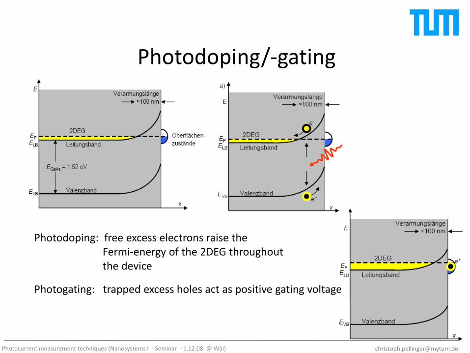
Photodoping/-gating
Photodoping: free excess electrons raise theFermi-energy of the 2DEG throughout the device
Photogating: trapped excess holes act as positive gating voltage
____________________________________________________________________________________________________________________
Photocurrent measurement techniques (Nanosystems I - Seminar - 1.12.08 @ WSI) [email protected]
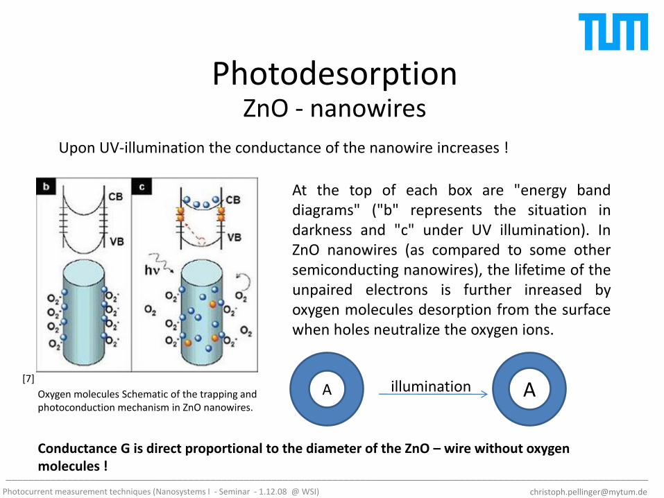
PhotodesorptionZnO - nanowires
Upon UV-illumination the conductance of the nanowire increases !
Oxygen molecules Schematic of the trapping and photoconduction mechanism in ZnO nanowires.
At the top of each box are "energy banddiagrams" ("b" represents the situation indarkness and "c" under UV illumination). InZnO nanowires (as compared to some othersemiconducting nanowires), the lifetime of theunpaired electrons is further inreased byoxygen molecules desorption from the surfacewhen holes neutralize the oxygen ions.
illumination AA
Conductance G is direct proportional to the diameter of the ZnO – wire without oxygen molecules !
[7]
____________________________________________________________________________________________________________________
Photocurrent measurement techniques (Nanosystems I - Seminar - 1.12.08 @ WSI) [email protected]
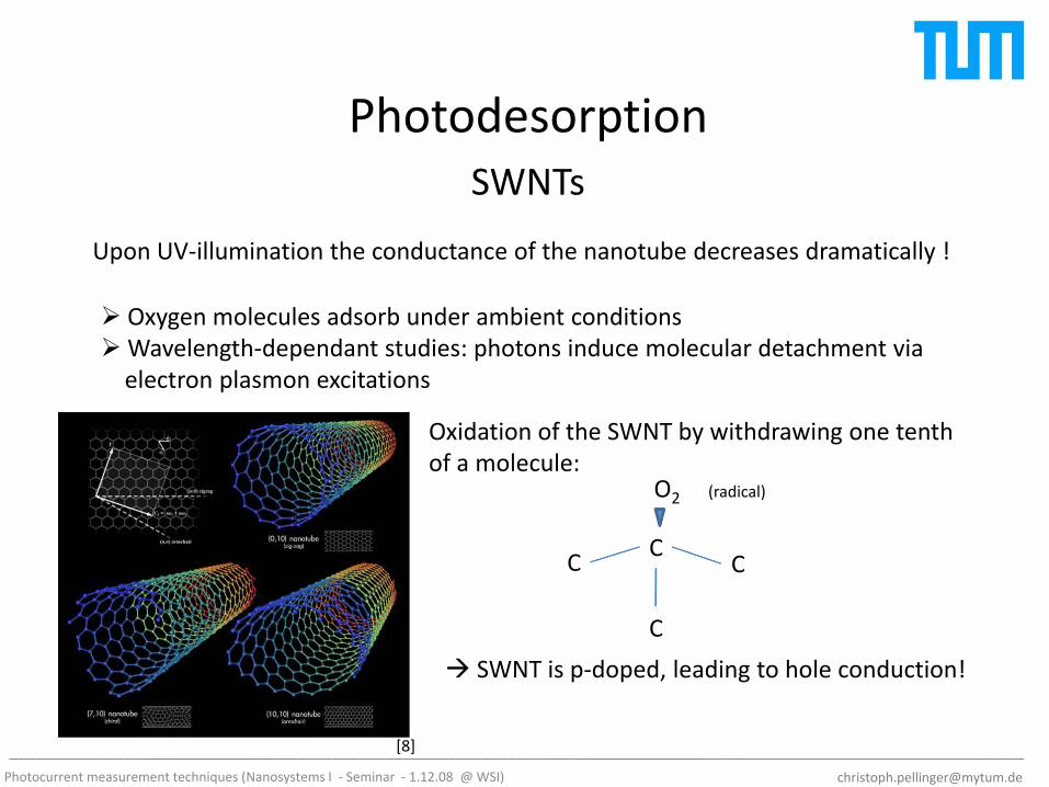
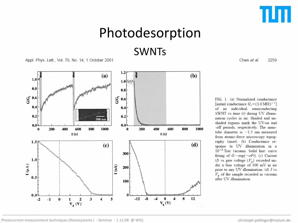
PhotodesorptionSWNTs
C C
C
C
O2 (radical)
Upon UV-illumination the conductance of the nanotube decreases dramatically !
Oxygen molecules adsorb under ambient conditionsWavelength-dependant studies: photons induce molecular detachment via
electron plasmon excitations
Oxidation of the SWNT by withdrawing one tenth of a molecule:
SWNT is p-doped, leading to hole conduction!
[8]
____________________________________________________________________________________________________________________
Photocurrent measurement techniques (Nanosystems I - Seminar - 1.12.08 @ WSI) [email protected]
PhotodesorptionSWNTs
Chopper
Gärtn
er
Laser
xy
A.W. Holl
Sou
rce
Dra
in
1000
920
840
780
740
700
660
620
580
540
500
460
420
380
340
Ti:SaN
L Fiber
BB
O
+/-
____________________________________________________________________________________________________________________
Photocurrent measurement techniques (Nanosystems I - Seminar - 1.12.08 @ WSI) [email protected]
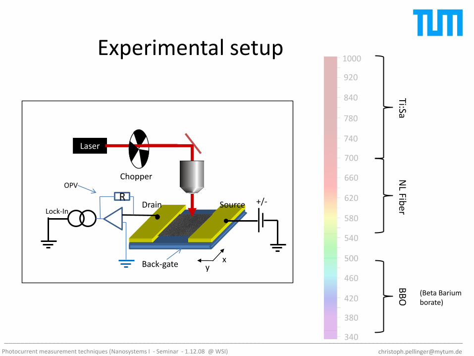
Experimental setup
Drain
Back-gate
SourceR
OPV
Lock-In
(Beta Barium borate)
____________________________________________________________________________________________________________________
Photocurrent measurement techniques (Nanosystems I - Seminar - 1.12.08 @ WSI) [email protected]
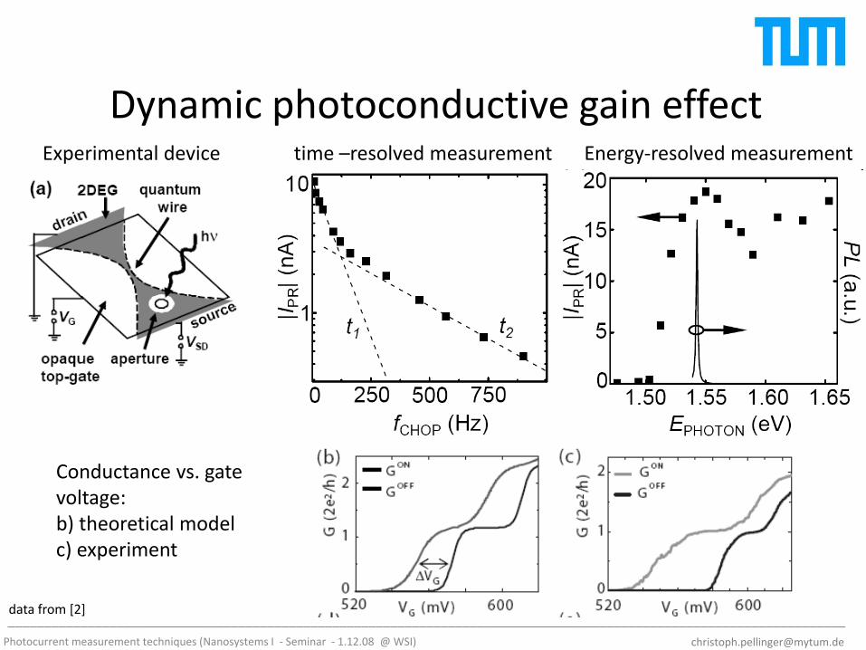
Dynamic photoconductive gain effectExperimental device
Conductance vs. gate voltage: b) theoretical modelc) experiment
time –resolved measurement Energy-resolved measurement
data from [2]
____________________________________________________________________________________________________________________
Photocurrent measurement techniques (Nanosystems I - Seminar - 1.12.08 @ WSI) [email protected]
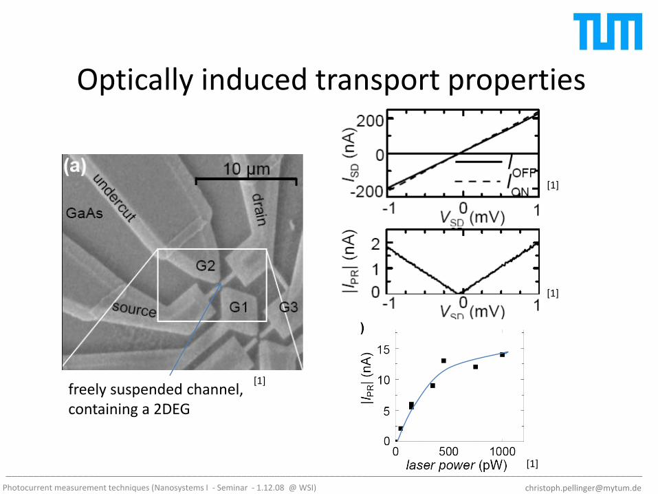
Optically induced transport properties
[1]
[1]
[1]
[1]
freely suspended channel, containing a 2DEG
____________________________________________________________________________________________________________________
Photocurrent measurement techniques (Nanosystems I - Seminar - 1.12.08 @ WSI) [email protected]
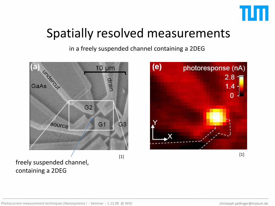
Spatially resolved measurements
freely suspended channel, containing a 2DEG
[1] [1]
in a freely suspended channel containing a 2DEG
____________________________________________________________________________________________________________________
Photocurrent measurement techniques (Nanosystems I - Seminar - 1.12.08 @ WSI) [email protected]
Literature [1] C. Rossler, K.-D. Hof, S. Manus, S. Ludwig, J.P. Kotthaus, J.Simon, A. W. Holleitner, D. Schuh, W.Wegscheider: „Optically induced transport properties of freely suspended semiconductor submicronchannels“
[2] K.-D. Hof, C. Rossler, S. Manus, J.P. Kotthaus, A. W. Holleitner, D. Schuh, W. Wegscheider: „Dynamic photoconductive gain effect in shallow-etched AlGaAs/GaAs quantum wires “
[3] Robert J. Chen, Nathan R. Franklin, Jing Kong, Jien Cao, Thomas W. Tombler, Yuegang Zhang, Hongjie Dai: „Molecular photodesorption from single-walled carbon nanotubes“ (Appl. Phys. Lett., Vol. 79, No. 14 (2001))
[4] Peidong Yang, Haoquan Yan, Samuel Mao, Richard Russo, Justin Johnson, Richard Saykally, NathanMorris, Johnny Pham, Rongrui He, Heon-Jin Choi: „Controlled Growth of ZnO Nanowires and TheirOptical Properties“ (Adv. Funct. Mater. 2002, 12, No. 5, May)
[5] Prof. Dr. Rudolf Gross und Dr. Achim Marx: Festkörperphysik – Vorlesungsskript zur Vorlesung im WS 2004/2005
[6] Sze: „Physics of semiconductor devices“
[7] http://nanotechnologytoday.blogspot.com/2007_04_01_archive.html
[8] www.wikipedia.org
[9] http://www1.tu-darmstadt.de/fb/ms/fg/ofl/lehre/scripte/schottky.pdf
!!! Thank you for your attention !!!
Special thanks to:
Leonhard Prechtel
&
Prof. Dr. A. W. Holleitner