petastar: a petabit photonic packet switch - selected areas in
TRANSCRIPT

1096 IEEE JOURNAL ON SELECTED AREAS IN COMMUNICATIONS, VOL. 21, NO. 7, SEPTEMBER 2003
PetaStar: A Petabit Photonic Packet SwitchH. Jonathan Chao, Fellow, IEEE, Kung-Li Deng, Member, IEEE, and Zhigang Jing, Member, IEEE
Abstract—This paper presents a new petabit photonic packetswitch architecture, calledPetaStar. Using a new multidimensionalphotonic multiplexing scheme that includes space, time, wave-length, and subcarrier domains, PetaStar is based on a three-stageClos-network photonic switch fabric to provide scalable large-di-mension switch interconnections with nanosecond reconfigurationspeed. Packet buffering is implemented electronically at theinput and output port controllers, allowing the central photonicswitch fabric to transport high-speed optical signals without elec-trical-to-optical conversion. Optical time-division multiplexingtechnology further scales port speed beyond electronic speed up to160 Gb/s to minimize the fiber connections. To solve output portcontention and internal blocking in the three-stage Clos-networkswitch, we present a new matching scheme, called c-MAC, aconcurrent matching algorithm for Clos-network switches. Itis highly distributed such that the input–output matching androuting-path finding are concurrently performed by schedulingmodules. One feasible architecture for the c-MAC scheme, wherea crosspoint switch is used to provide the interconnections be-tween the arbitration modules, is also proposed. With the c-MACscheme, and an internal speedup of 1.5, PetaStar with a switchsize of 6400 6400 and total capacity of 1.024 petabit/s can beachieved at a throughput close to 100% under various trafficconditions.
Index Terms—Clos network, optical time-division multiplexing(OTDM), packet scheduling, photonic switch.
I. INTRODUCTION
T HE INTERNET has become a fundamental driving forcefor a variety of information technologies due to its ever-
growing ability to handle traffic, its ubiquitousness, and the ser-vices [1]. New applications, such as sensor fusion, bio-infor-matics, grid computation, global data storage, and on-line videoapplications are emerging. Common among these applicationsis their demand for a huge amount of bandwidth and a globalpacket switching infrastructure. In contrast to the success in in-creasing the raw bandwidth for terabit transmission capabilityusing dense wavelength division multiplexing (DWDM) tech-nology toward the end of the last century [2]–[5], today’s elec-tronic router technology may soon exhaust its capacity of a fewterabit/s [6]–[8]. To find a cost-effective way to build a routerwith a few tens of terabit or even petabit capacity will be thekey to the continuing success of the next-generation Internet[9]–[12].
Manuscript received August 1, 2002; revised March 31, 2003. This work wassupported in part by the National Science Foundation under Grant 9814856 andGrant 9906673 and in part by the New York State Center for Advanced Tech-nology in Telecommunications.
H. J. Chao and Z. Jing are with the Department of Electrical and ComputerEngineering, Polytechnic University, Brooklyn, NY 11201 USA (e-mail:[email protected]; [email protected]).
K.-L. Deng is with the Global Research Center, General Electric Company,Niskayuna, NY 12309 USA (e-mail: [email protected]).
Digital Object Identifier 10.1109/JSAC.2003.815678
While electronics has been widely used in building largebuffers and high-speed packet schedulers [13]–[16] in routers,it is still very difficult to build a large-dimension (beyond 1000
1000) electronic switch fabric with an OC-192 (10-Gb/s)line rate. Currently, electronic crossbar switches can be im-plemented on a single chip with a capacity of up to 320 Gb/sat a link rate of 2.5 Gb/s [17]. To build a petabit (10Gb/s)switch fabric with a three-stage Clos-network, the dimensionof interconnection may reach 100 000 with the port rate at10 Gb/s. The total number of interconnections can be estimatedas: 100 000 (connections between stages)2 (stages) 4(number of 2.5-Gb/s electronic planes to form a 10-Gb/s port)
800 000 (interconnections). This large number of fiberinterconnections for an electronic switch fabric becomes toocomplex to implement (or even manage). Thus, we are moti-vated to look into a photonic switch system as an alternative forbuilding a petabit switch fabric.
Several promising photonic technologies have been pro-posed in the implementation of large-dimension space switches[18]–[20]. The optical microelectromechanical system (MEMS)has demonstrated a 12961296 cross-connection switch witha total capacity of 2.07 petabit/s [21]. The drawback to thesetypes of switches is the slow reconfiguration speed (in thesor ms range) because of moving and stabilizing the mechanicsof the mirrors. For packet switching, the switch fabric needsto reconfigure its connections on a per-packet basis, usuallyin the nanosecond time scale. Another alternative for buildinga photonic switch fabric is to combine tunable lasers with anarray waveguide grating (AWG) [22]–[25] device as a spaceswitch. The advantage of this approach is the rapid switchingspeed achieved by tuning the wavelength of the lasers at ananosecond speed [26]–[28]. When cascading the AWG-baseddevices for a multistage switch fabric, wavelength conversionbecomes an essential element because the switching property ofthe AWG depends on the change of the input wavelengths [29].All-optical wavelength conversion has been achieved usingnonlinear effects in either electro-optic crystal [30] or opticalfibers [31]. However, to fully exploit nonlinearity, the powerrequirements on these methods may not be practical in systemapplications. Another approach is to use resonance nonlinearityin semiconductor optical amplifiers [32], [33], which has highernonlinearity than the other media. The power requirement ofsuch an approach can be as low as tens of femto-joules perpulse, suitable for large-scale system applications.
We previously proposed a single-stage photonic packetswitch fabric with a capacity of up to several terabit/s [34].Here, we present a new photonic packet switch architecturewith petabit/s switching capacity for next-generation routers,called PetaStar. The switching fabric uses multidimensionalphotonic technologies to achieve highly scalable, rapidlyreconfigurable interconnections in a three-stage Clos network.Packet buffering is implemented electronically outside the
0733-8716/03$17.00 © 2003 IEEE

CHAO et al.: PETASTAR: PETABIT PHOTONIC PACKET SWITCH 1097
Fig. 1. System architecture of the PetaStar.
central photonic switch fabric, allowing the high-speed opticalsignals being transported without electrical-to-optical conver-sion. We believe this is more practical than those switches thatuse optical delay lines as buffers [35]. This is because opticalmemory technology is still immature and its size is very small,e.g., a few tens of packets. Optical time-division multiplexing(OTDM) techniques [36]–[38] are used to increase the portspeed to hundreds of gigabit/s. Based on the PetaStar, a 6400
6400 switch can be realized using 80 wavelengths foreach individual switch module in a three-stage Clos networkarchitecture. With the port speed of 160 Gb/s, a total switchcapacity reaches 1.024 petabit/s. The number of fiber intercon-nections is greatly reduced by aggregating more bandwidth ona single fiber. With the above example of building a 100 000
100 000 switch with the port rate at 10 Gb/s, the total fiberinterconnections are reduced from 800 000 to 12 000, makingthe proposed architecture more feasible for implementation.The reduction is contributed by increasing the bandwidth offiber interconnections from 2.5 to 160 Gb/s.
Although there are many effective scheduling schemesthat have been proposed to resolve output contention forsingle-stage switches [39]–[57], until now, only a few matchingschemes for Clos-network switches have been proposed [15],[16], where the first and the third stages have shared-memorybuffers, thus limiting the switch capacity. It is very challengingto find an efficient and fast scheduling scheme to provide highperformance under various traffic conditions in the three-stagebufferless Clos-network switch, such as the PetaStar. Thescheduling scheme must be able to scale gracefully with a
large switching capacity because the time for resolving outputcontention becomes more constrained with the increase ofswitch size and port speed. This paper presents a new matchingscheme, called c-MAC, a concurrent matching algorithm forClos-network switches. It is highly distributed such that theinput–output (I/O) matching and routing path finding areconcurrentlyperformed by scheduling modules. To relax thestrict arbitration time constraint and round-trip delay betweenline cards and the packet scheduler (and to accommodateslow-configuration optical switch fabrics), c-MAC operates ona frame basis, consisting ofcells ( ). To improve I/Omatching efficiency, c-MAC slightly modifies the exhaustivedual round-robin matching (EDRRM) scheme [54] to improvethroughput under various traffic conditions. The throughputof the c-MAC scheme is close to 100% under various trafficdistributions at a cost of internal speedup of 1.5. A feasibleimplementation of the c-MAC scheme, where a crosspointswitch is used to provide the interconnection between thearbitration modules, is also proposed.
The paper is arranged as follows. Section II describes thesystem architecture including the data structure, the packetflow, and the design of electronic buffering at the input portcontroller and output port controller. Section III presentsthe c-MAC packet-scheduling scheme for the three-stageClos-network switch. It also shows the implementation com-plexity of the c-MAC packet scheduler and its performancestudy results. Section IV details the implementations ofthe proposed photonic switch fabric. Section V presents ourconclusions.

1098 IEEE JOURNAL ON SELECTED AREAS IN COMMUNICATIONS, VOL. 21, NO. 7, SEPTEMBER 2003
Fig. 2. Data packet flow.
II. SYSTEM ARCHITECTURE
A. Petabit Photonic Packet Switch Architecture
Fig. 1 shows the system architecture of the proposed petabitphotonic packet switch, called PetaStar. The basic buildingmodules include the input and output port controllers (IPCs andOPCs), input grooming and output demultiplexing modules(IGMs and ODMs), photonic switch fabric (PSF), centralizedpacket scheduler (PS), and a system clock distribution unit.The PSF is a three-stage Clos-network with columns of inputswitch modules (IMs), central switch modules (CMs), andoutput switch modules (OMs). The incoming and outgoing linerates are assumed to be 10 Gb/s. All incoming lines will first beterminated at line cards (not shown in the figure), where packetsare segmented into cells (fixed length data units) and storedin a memory. The packet headers are extracted for IP addresslookup.1 All cell buffering is implemented electronically atthe IPCs and OPCs, leaving the central PSF bufferless, i.e., nophotonic buffering is required in the system. As a result, thebit rate of each port can operate at a speed beyond the limits ofthe electronics. The port speed can be equal to or greater than(with a speedup) times the line rate, whereis the groomingfactor. Virtual output queues (VOQs) at IPCs, together with thePS, provide contention resolution for the packet switch. At theinput end, the majority of incoming packets are stored in theingress line cards, where packets are segmented and stored inits VOQs. Packets destined for the same output port are storedin the same VOQ. VOQs implemented at the IPC serve asthe mirror of the VOQ memory structure in the line cards. Aslong as they can keep the cells flowing between the line cardand IPC, the size of the VOQs at the IPC can be considerablysmaller than its mirror part in the ingress line cards. Buffers atthe OPC are used to store cells before they are sent out to thedestined egress line cards. A large buffer with a virtual inputqueue (VIQ) structure implemented in the line card (not shown
1Functions such as classification and traffic shaping/policing are usually per-formed at the edge routers, but not at core routers.
in the figure) is used to store the egress cells from the PSF andreassemble them into packets.
Fig. 2 shows how packets flow across the system. At the input,variable-length IP packets are first segmented into cells with afixed length of 64 B (including some cell overhead), suitable toaccommodate the shortest IP packet (40 B). At each IPC, a totalof input lines at 10 Gb/s enter the system and terminate at theIPC. To reduce memory speed, each VOQ has a parallel memorystructure to allow cells to be read at the same time. Thesecells form a photonic frame. Each cell, before entering the IGMfor compression, is scrambled to guarantee sufficient transitionsin the data bits for optical receiver and clock recovery. In theIGM, these cells are compressed at the optical time domain toform a time-interleaved OTDM frame at Gb/s. Let bethe cell time slot and ns for 10-Gb/s line rate. Let bethe compressed cell time slot at the port speed ( Gb/s)and B/( Gb/s), where is the speedup factor.Then, the compressed photonic frame period
B/( Gb/s). With and , the frameperiod is equal to the cell slot, . Guardtime is added at thehead of the frame to compensate for the phase misalignment ofthe photonic frames when passing through the PSF and to coverthe transitions of optical devices.
At each stage of the photonic switching fabric, the corre-sponding subcarrier header is extracted and processed to controlthe switching fabric. Since the PS has already resolved the con-tention, the photonic frame is able to find a path by selecting theproper output links at each stage in the switching fabric. Oncethe photonic frame arrives successfully at the designated outputport, it is demultiplexed and converted back tocells at 10 Gb/sin the electronic domain by the optical demultiplexing module.The OPC then forward the cells to their corresponding line cardsbased on the output line numbers (OLs).
As Figs. 1 and 2 show, the optical signals run between theIGM and the ODM at a rate of Gb/s, or 160 Gb/s for
. All optical devices/subsystems between them operateat Gb/s. However, the electronic devices only operate atmost 10 Gb/s (with speedup of one), or even lower with parallel

CHAO et al.: PETASTAR: PETABIT PHOTONIC PACKET SWITCH 1099
Fig. 3. Data structure of (a) incoming cell, (b) compressed cells, and (c) photonic frame.
wires, e.g., fourSERDESsignals, each at 2.5 Gb/s (or 3.125Gb/s including 8B/10B coding).
Fig. 3 illustrates the data structure at each stage of the switch.Before the data payload, two header fields that contain the OLin the destined output port and the input line number (IL) ofthe switch are added to each incoming cell [see Fig. 3(a)]. TheOL is used to deliver cells to the destined output lines whenthe photonic frame (cells) arrives at the OPC. A validity bitis inserted at the beginning of the cell to indicate if the cell isvalid or not. The overhead bits introduced by OL and IL canbe calculated as and , respectively. Forexample, for a petabit system with and ,the cell header length is 21 bits (1 4 16). Bits in eachcell are compressed and time-interleaved using optical time-di-vision multiplexing (OTDM) techniques in the IGM to form thephotonic frames that are ready to transmit through the PSF [seeFig. 3(b)]. Each photonic frame goes along with an out-of-bandsubcarrier (SC) header. Using the photonic frame as its carrier,the SC header is amplitude-modulated on the photonic frameat a much lower subcarrier frequency. The estimated raw band-width required for the SC header is about 600 MHz. Standardmultilevel coding schemes can be applied to further compressthe SC bandwidth to 80 MHz or less, allowing the SC headerto be carried around the dc frequency. The first field in the SCheader is a flag containing a specific pattern for frame delin-eation since the photonic frames carrying the SC header do notprecisely repeat in the time domain. The payload is 8B/10Bcoded for correctly finding the flag. Three fields are attachedto the SC header to provide routing information at each stage ofthe PSF. The three fields include CM, OM, and OPC numberswith , , and bits of information, where
and are the numbers of CM and OM, andis the numberof outputs at each OM. At the beginning of the frame, a validitybit is added to indicate if the frame contains valid cells.
Fig. 4 gives an example of how cells flow through the IPC.In this case, packets , , and from input lines 1 and ,respectively, are destined for the same output port of the PSF(port 1). Packets and are heading toward output line 1while packet C is headed toward output lineat the same OPC.Upon arriving at the IPC, each packet, already segmented intoa number of fixed-size cells, is stored in the correspondinginput line memory. In this example, packet A is segmentedinto 24 cells (cells to ), packet B contains 16 cells(cells to ), and packet has 8 cells (cells to ).All incoming cells are stored in the r frame memories in around-robin manner.
As soon as a cell arrives at the input line memory, a request issent to the packet scheduler that tracks of all the incoming cells.The scheduler, based on a new hierarchical frame-based exhaus-tive matching scheme, sends back the grant signal if the trans-mission has been granted. As a result, 16 cells (to ) frominput line memory 1 are selected at the first frame period to formframe number 1, followed by 16 cells ( to ) from inputline memory selected at the next frame period to form framenumber 2. In this example, the remaining eight cells ( to
) will be aggregated with another eight cells from C packet( to ) to form frame number 3. The reason that packetis granted prior to the second half of packet A is because packetB has a filled frame and thus has a higher priority for transmis-sion. At the IGM, cells are compressed into the time-interleavedphotonic frames and thus ready to be routed through the PSF.
Following the above example, Fig. 5 shows how packets, and are processed as they are demultiplexed at the
OPC and reassembled at the egress line cards. Photonic framescontaining the compressed cells are demultiplexed in the ODMand sent into parallel inputs of the selector array. Accordingto the cell header, to go to the 16 first-in–first-outs(FIFOs) located in output line memory 1 at the first frame

1100 IEEE JOURNAL ON SELECTED AREAS IN COMMUNICATIONS, VOL. 21, NO. 7, SEPTEMBER 2003
Fig. 4. An example of illustrating how frames are formed in the IPC.
Fig. 5. An example of illustrating how packets are demultiplexed at the OPC and reassembled at the egress line cards.
period. At the next frame period, to are sent to the same16 FIFOs in output line memory 1. At the next frame period,photonic frame number 3 arrives at the OPC. The remainingpart of packet is sent to input line memory 1, while cellsfrom packet go to output line memory. These cells are thenread out from the FIFOs to the designated output line (outputline 1 in this case) at a speed larger than 10 Gb/s. The VIQs atthe line card are used to reassemble packets, , and .
Synchronization can be challenging as the system scales.To achieve synchronization, a centralized frame clock willbe supplied to each module in the system. Each switching
action, including buffer reading and writing, switching of laserwavelength, and OTDM multiplexing and demultiplexing, willbe synchronized according to the same frame clock signal witha frequency of, e.g., 1/51.2 ns, or19.5 MHz. The clock signalwill be distributed among the modules using optical signalsthrough fibers to provide a sharp stroke edge for triggeringoperations. A sinusoidal signal at 10 GHz will be distributedto each module as the base frequency for the synchronization.The subcarrier provides a trigger signal at each switching stage.Upon detecting the subcarrier signal in the subcarrier unit(SCU), which indicates the arrival of a photonic frame at the

CHAO et al.: PETASTAR: PETABIT PHOTONIC PACKET SWITCH 1101
input of the module, the SC processor will wait for a precisetime delay before starting the switching operation. The timedelay through the fiber connections will be chosen precisely[58] so that it can accommodate the longest processing delay inthe header process. The minimum timing tolerance contributedby both photonic and electronics devices, as well as fiberlength mismatch in the system, will ultimately determine theguardtime between the photonic frames. For instance, witha frame period of 51.2 ns and 10% used for the guardtimeoverhead, the guardtime can be5 ns, which is sufficientlylarge to compensate for the phase misalignment, fiber lengthmismatch, and optical device transitions.
III. PACKET SCHEDULING FOR THETHREE-STAGE
CLOS-NETWORK SWITCH
One of the most complex units in this architecture is thepacket scheduler (PS). It first resolves the contention of theframes from different input ports that are destined for thesame output port. It then determines a routing path through thecenter stage (i.e., chooses a CM) for each matched I/O pair.Since there can be multiple possible paths (determined by thenumber of CMs) for each matched I/O, how to choose a CMto reduce internal blocking and thus increase the throughputfurther complicates the scheduling algorithm design.
For an input-buffered switch with a VOQ structure, severalmaximum-weight matching (MWM) algorithms have beenproposed to achieve 100% throughput for independent andidentically distributed (i.i.d.) arrivals (uniform or nonuniform).Some theoretical results for delay bound have been determined[39]–[43]. But MWM is not practical to implement in hardwaredue to its high complexity. In [44]–[47], some scheduling algo-rithms for VOQ switches with speedup 2 can exactly emulate anoutput-queued switch. The maximal matching algorithm [40],[48] is more practical than MWM, and it has been proven tobe stable with a speedup of 2 [49], [50]. A randomized sched-uling algorithm presented by Tassiulaset al. [51] guarantees100% throughput with low complexity but high delay. Otherpractical iterative matching algorithms such as PIM [52], iSLIP[53], and DRRM [9], use multiple iterations to converge on amaximal-size matching.
With the increase of switch size and port speed, arbitrationtime to resolve the output port contention becomes verystringent. To relax the stringent arbitration time constraint,several schemes that use large time scales have been proposed[55]–[57]. In [55], a new method of using large frame sizes isproposed for switching variable-sized packets over a crossbarswitch to minimize reconfiguration frequency of the switchfabric. This method provides attractive delay bounds. However,it not only requires more than schedulers ( is the switchsize) in the system, it also requires each scheduler to performsophisticated packet scheduling schemes, such as weightedfair queueing or shaped virtual clock, which are prohibitivelycostly. In [56], time slots are grouped into a frame. Con-tentions are solved and a set of matching is generated at eachframe boundary and during a frame the switch fabric is updatedat most times. In [57], a batch of requests is accumulated anda corresponding schedule for a constrained switch is generated.However, to achieve high performance, those schemes sufferhigh time complexity.
A. Packet Scheduler Architecture
Fig. 6 shows an implementation architecture for the PS,which consists of scheduling input modules (SIMs) andscheduling output modules (SOMs), each of which correspondsto an input switch module (or output switch module) in thethree-stage Clos-network switch (see Fig. 1). There areinput port arbiters (IPAs) divided into groups, IPAs are ineach SIM. Each SIM consists of virtual output port arbiters(VOPAs), each of which corresponds to an output port in thecorresponding OM. Each SIM has an input module arbiter(IMA), and each SOM has an output module arbiter (OMA). Acrosspoint switch with a predetermined reconfigured pattern isused to interconnect these SIMs and SOMs.
As discussed in Section II, each IPC hasVOQs, eachcorresponding to an OPC. Each consists of
accepting cells from input lines, wheredenotes the IPC number, denotes the OPC number, anddenotes the input line number. A counter is used torecord the number of cells in the corresponding .An is used to record the total number of cells in each
. So, . Each input portarbiter, corresponding to each input port of the PSF, maintains
line arbiters s. When IPC is matched with an OPC,say , the line arbiter , based on the value of each
, chooses cells from input lines to form a frame.
B. Concurrent Matching Algorithm for Clos-Network Switch(c-MAC)
This section describes a new Concurrent Matching Algorithmfor Clos-network switches, called c-MAC, to match the inputand output ports of the PSF and to find routing paths throughthe CMs. Here, we extend the switching unit from a cell to aframe of cells that are contributed byinput lines in the samegroup. For instance, letting , the period of a photonicframe at 160 Gb/s is equal to a cell time slot at 10-Gb/s line, i.e.,51.2 ns. The c-MAC scheme divides one frame periodinto
matching cycles as shown in Fig. 7. In each matching cycle,each SIM is matched with one ofSOMs. The c-MAC schemeduring each cycle includes two phases to find the I/O matchesand routing paths, respectively.
To achieve high I/O matching efficiency, the exhaustive dualround-robin matching (EDRRM) scheme [54] is slightly modi-fied here. Most iterative matching schemes, such as iSLIP [53]and DRRM [9], suffer from the problem of throughput degrada-tion under unbalanced traffic distribution. The EDRRM schemeimproves throughput by maintaining the existing matched pairsbetween the inputs and outputs so the number of unmatched in-puts and outputs is drastically reduced (especially at high load),thus reducing the inefficiency caused by not being able to findmatches among unmatched inputs and outputs. One of the majorproblems of the EDRRM is that it may cause starvation in someinputs. One way to overcome this problem is to limit the max-imum number of cells that can be continuously transmitted fromeach input port.
At the beginning of each cycle, each SOM passesbits to the corresponding SIM as shown in Fig. 7, wherebitcorresponds to the state of input links of the correspondingOM; bit corresponds to the state ofoutput ports of the cor-responding OM. There are four possible states for each output

1102 IEEE JOURNAL ON SELECTED AREAS IN COMMUNICATIONS, VOL. 21, NO. 7, SEPTEMBER 2003
Fig. 6. Schematic of the packet scheduler.
Fig. 7. Timing schematic of the c-MAC scheme.
port: “00” when the output port is unmatched; “01” when theoutput port is matched with low priority in the last frame pe-riod; “10” when the output port is matched with high priority inthe last frame period; “11” when the output port is matched inthis frame period.
Here, we assume the matching sequence between SIMs andSOMs is predetermined. For instance, in the first cycle, SIMismatched with SOM, where ; . In thesecond cycle, SIMis matched with SOM . The pro-cedure is repeatedtimes. To achieve matching uniformity forall the SIMs, the beginning matching sequence between SIMsand SOMs is skewed one position at the beginning of each frameperiod.
Phase 1: Find I/O Matches:Phase 1 consists of three steps asdescribed below.
Step 1) Request:• Each matched IPA only sends a high-priority request to
its matched VOPA; each unmatched IPA (including thecurrently matched IPA but whose matched VOQs queuelength is less than a threshold) sends a 2-bit request
to every VOPA for which it has queued cells in the cor-responding VOQ. [“00” means no request; “01” meanslow-priority request because queue length is less than;“10” means high-priority request because queue lengthis large than ; “11” means the highest priority becausethe waiting time of the head-of-line (HOL) frame is largerthan a threshold, ].
Step 2) Grant:• Only the “available” VOPA performs the grant operation.
A VOPA is defined to be “available,” if its correspondingoutput port is
a) unmatched; orb) matched in the last frame period with low priority
(the VOPA receives at least one high-priority re-quest at this frame period); or
c) VOPA is matched in the last frame period with highpriority, but it receives the request from the matchedIPA and its priority is becoming low-priority at thisframe period.
• If a VOPA is “available” and receives one or more high-priority requests, it grants the one that appears next in afixed round-robin schedule starting from the current posi-tion of the high-priority pointer. If there are no high-pri-ority requests, the output port arbiter grants one low-pri-ority request in a fixed round-robin schedule starting fromthe current position of the low-priority pointer. The VOPAnotifies each requesting IPA whether or not its request isgranted.
Step 3) Accept:• If the IPA receives one or more high-priority grants, it
accepts the one that appears next in a fixed round-robinschedule starting from the current position of the high-pri-ority pointer. If there are no high-priority grants, the input

CHAO et al.: PETASTAR: PETABIT PHOTONIC PACKET SWITCH 1103
Fig. 8. (a) Illustration of parallel matching with local optimization by grouping two SIMs and SOMs together. (b) Achieves one more match than (c) by choosinglink L first.
port arbiter accepts one low-priority request in a fixedround-robin schedule starting from the current positionof the low-priority pointer. The input port arbiter notifieseach VOPA whether or not its grant is accepted.
• Update of the pointers: The pointer of IPA and VOPA isupdated to the chosen position only if the grant is acceptedin Step 3 of phase 1 and also accepted in phase 2.
Phase 2: Find Routing Paths for the Matched I/O Pairs.AfterI/O matching is completed in phase 1, c-MAC finds a routingmatch (or routing path) for each matched I/O pair through thethree-stage bufferless Clos-network switch. Finding a routingpath is equivalent to finding an available CM (out ofCMs) forthe matched I/O pair. When , the three-stage Clos-network is a nonblocking circuit switch. Although it has beentheoretically proven that a three-stage bufferless Clos-networkswitch is rearrangeably nonblocking when , the alreadyknown rearrangement scheme is impractical to implement in thehigh-speed switch due to the prohibitive high time complexity.For instance, some recent research results show that the “EulerSplit” scheme has a time complexity of [59], where
is the switch port size. To reduce computation complexity, asimple parallel matching scheme [60], [61] is adopted. Let uslabel the set of output links of each SIMby ( ) andthe set of input links of each SOMby ( ), as shownin Fig. 8. Each and contains exactly elements denotingthe state of each physical link, i.e., ,
. Note that each “0”means that this link has not been matched; otherwise,
“1.” To find a path between SIMand SOM, one just needsto find a vertical pair of zeros in and .
To improve the matching efficiency of the parallel matchingscheme, we propose the following two methods.1) When searching for vertical zero pairs in the and ,
choose those that are not occupied by any SIM and SOM inthe last frame period. This improves the efficiency of findingrouting paths by intentionally making routing paths avail-able to those I/O pairs that are matched in the last frame
period. In other words, the spirit of exhaustive matching isfurther extended from I/O matching to internal path finding.
2) Group multiple SIMs (or SOMs) together into the same de-vice (e.g., of them with ) to achieve local optimiza-tion of routing resources. However, this increases the I/Obandwidth of the device, thus limiting the number of SIMs(or SOMs) that can be integrated in the same device.
Based on the exhaustive matching policy in phase 1, thec-MAC scheme maintains a register ( ) for each SIM(SOM ). has a structure similar to the ( ). Eachand contains exactly elements, each denoting the matchingstate of each physical link at the end of the previous frameperiod, , .When an IMA receives the accept information from VOPAs,it performs parallel matching between SIMand SOM to findthe routing paths between SIMand SOM. While finding avertical pair of zeros in the and , it takes into account thestate of and . It first picks an available link unmatched inthe last frame period (i.e., ). Ifno such output links can be found, it picks any unmatched linksinstead (i.e., ). If no unmatched links can befound for the matched I/O pair, the “accept” in step 3 of phase1 is changed to “reject.”
Fig. 8(a) shows an example of the group size . SIMand SIM are integrated into group SIM-G, while SOM andSOM are integrated into group SOM-G.When performingparallel matching between SIM-Gand SOM-G, all the linkstate information (including SOM and SOM) is sent toSIM-G . Within SIM-G , parallel matching between SIMand SOM is performed by finding a vertical pair of zerosin the and (i.e., ). The link stateinformation of SOM is also examined. We first pick thosezero pairs, for which SOMhas already matched with anotherSIM (i.e., ). This leads to more matching opportunitieswhen SIM is to match with SOM later. For instance, bychoosing link first, Fig. 8(b) results in one more match thanFig. 8(c).

1104 IEEE JOURNAL ON SELECTED AREAS IN COMMUNICATIONS, VOL. 21, NO. 7, SEPTEMBER 2003
When phase 2 is complete, each SIM passes bit (linkstate information and output port matching results) to the corre-sponding SOM. Each SIMupdates its and ; each SOMupdates its and accordingly. Note that at the beginning ofeach frame period, and are reset to zero.
C. Packet Scheduler (PS) Time Complexity
Here, we estimate the time complexity of the PS. Let us as-sume , , , the amountof information that needs to be transmitted from each IPC tothe PS is 26 B [ (6400) bit] per time slot, or about4 Gb/s. In return, the PS sends back the matching results to eachIPC that becomes the cell headers of the frame, and to each IGMthat becomes the in-band header of the frame. The former has atotal of 93 bits (13 80) and the latter has a total of 30 bits (7
7 7 1 8). Thus, the bandwidth is about 1.8 Gb/s fromthe PS to the IPC and 600 Mb/s from the PS to the IGM.
Let us estimate the required frame periodto finish thec-MAC arbitration. Assume that group size is set tomodulesas shown in Fig. 8; the I/O bandwidth of one chip is BW;the time spent for I/O matching and finding routes within theSIM in each matching cycle is . Because of grouping,the number of required matching cycles is reduced to,while the information between a SIM and a SOM increases to
. So, can be estimated as
(1)
For example, when assuming , ns,Gb/s, , should be set larger than 496 ns,
equivalent to 10 cells at 10-Gb/s line rate, or 160 cells at160-Gb/s port speed. The total switching capacity of the cross-point switch in Fig. 6 is 400 Gb/s 80, or 32 Tb/s, about 1/30of the photonic packet swtich fabric. The crosspoint switch canbe implemented with 160 switches in parallel, each with a 80
80 crosspoint chip at 2.5-Gb/s link speed (raw data rate at3.125 Gb/s [17]).
D. Performance Study
1) Performance of c-MAC in a Single-Stage NonblockingSwitch: The performance of the c-MAC scheme was evaluatedusing computer simulations for uniform and nonuniform trafficmodels. We first studied the performance of the c-MAC in asingle-stage nonblocking switch.2 The delay, in unit of celltime slot, is measured from when a cell enters the IPC to whenit arrives at the OPC.
Fig. 9 shows the throughput of c-MAC and iSLIP underBernoulli traffic with different unbalanced probabilities () andframe sizes () for a switch size ( ) of 64. is defined to be aportion of traffic that is sent to a particular output port with theremaining traffic evenly distributed to all others. When ,the traffic is uniformly distributed to all output ports. When
, it is circuit switching, meaning that the traffic fromeach input port is all destined for output port. The number ofiterations of finding matches in each frame period is set to one,
2It can also be a three-stage Clos-network switch withm � 2n � 1. Theperformance and impact ofm in a three-stage bufferless Clos network is furtherdiscussed in Section III-D2.
Fig. 9. Throughput of the c-MAC and iSLIP under Bernoulli traffic withdifferent unbalanced probabilities.
so is the average burst length. Both iSLIP and c-MAC achievevery high throughput under uniform traffic distributions. Theformer can even achieve 100% due to the desynchronizationof pointers in the input and output arbitrators. However, thelatter provides much higher throughput (close to 100%) underunbalanced distributions. This is because c-MAC significantlyreduces the number of unmatched inputs and outputs bymaintaining the existing matches, thus reducing output portcontention.
The c-MAC scheme still maintains high throughput with alarge frame size of 16. This is because filled frames havehigher priority than those unfilled to be served, thus providinghigher frame utilization. As a result, currently matched inputand output pairs may not be able to maintain matching if theircorresponding queue lengths are less than.
To avoid some pathological traffic conditions that may leadto starvation, the head-of-line (HOL) frame’s priority level isboosted to the highest when its waiting time exceeds a certainthreshold, say . When the HOL frame’s waiting time exceeds
, the input port arbiter only sends these highest-priority re-quests to the VOPAs, which then first grant the highest-priorityrequests. We assume that , , , and
in the simulations. Setting too small may breakalready established I/O pairs and adversely impact throughput.However, when is set as large as 16 000 (cell time) as shownin Fig. 10, high throughput, e.g., 0.98, can be achieved. This isbecause large waiting time thresholds will not break already es-tablished matches too often. Thus, starvation is prevented andhigh matching efficiency is maintained.
Fig. 11 shows the average delay of the c-MAC scheme withdifferent frame and switch sizes under uniform burst traffic. Weassume that the burst length is exponentially distributed withan average burst lengthof 16, observed at each input of theswitch fabric. Under the low traffic load, the average delay ofthe c-MAC scheme increases approximately proportionally withthe frame size. This is because an arriving cell must wait for thebeginning of the next frame if it is chosen under the frame-basedmechanism. However, at the high-load area, all VOQs tend to benonempty and the frames transmitted through the switch fabrictend to be full due to the priority mechanism introduced in the

CHAO et al.: PETASTAR: PETABIT PHOTONIC PACKET SWITCH 1105
Fig. 10. Throughput of the c-MAC in uniform Bernoulli traffic with differentwaiting time thresholdsT .
Fig. 11. Average delay, in the unit of cell time slotT, of the c-MAC schemeunder uniform bursty traffic with an average burst length of 16 cells for differentframe sizesr and switch sizesN .
c-MAC scheme. This explains that the impact of frame sizeon the average delay becomes less (i.e., delay curves gradu-ally converge) under heavy traffic load, and that close to 100%throughput is achieved even with large frame sizes and switchsizes as the traffic load approaches 100%.
2) Performance of c-MAC in a Three-Stage Clos-NetworkSwitch: Fig. 12 shows that the c-MAC scheme with local opti-mization, i.e., , [see Fig. 12(a)] can achieve much higherthroughput than that without local optimization [see Fig. 12(b)]in the three-stage Clos-network switch by considering differentCM numbers and speedup factors under unbalanced trafficdistribution. We assume of 2. With local optimization,
(a)
(b)
Fig. 12. Throughput comparison of the switch (a) with local optimizationand (b) without local optimization by considering different CM numbers andspeedup factors under unbalanced traffic.
even without bandwidth expansion (i.e., ), an internalspeedup of 1.5 can achieve close to 100% throughput in thethree-stage Clos-network switch. The throughput improvementis due to the fact that the existing matched routing pathsare maintained when performing parallel matching. Highermatching efficiency for routing paths is obtained by checkingfor more routing resources when SIMs and SOMs aregrouped together.
Fig. 13 shows the delay performance, including input delayat the IPC, output delay at the OPC, and the total delay (sum ofthe input and output delays) for different switch sizes without in-ternal bandwidth expansion, but with a small internal speedupof 1.5. We assume the service rate of the OPC is equal to theport speed. We evaluated the average delay under nonuniformburst traffic. Increasing the switch size to 256 does not affect thedelay performance much, especially under nonuniform trafficdistributions. This is because with an internal speedup of 1.5,most of frames have been transferred to the ELCs, where ex-cessive delay is expected. Thus, the overall delay performanceapproaches that of output-buffered switches.
IV. PHOTONIC SWITCH FABRIC (PSF)
A. Multistage PSF
Fig. 14 shows the structure of the PSF. It consists ofinputmodules (IMs), central modules (CMs), andoutput mod-

1106 IEEE JOURNAL ON SELECTED AREAS IN COMMUNICATIONS, VOL. 21, NO. 7, SEPTEMBER 2003
Fig. 13. Delay performance of the c-MAC scheme without expansion and withspeedup factor of 1.5 in a three-stage Clos-network switch.
Fig. 14. Photonic switching fabric (PSF) architecture. IM= input module,CM= central module, OM= output module, SCU= subcarrier unit, WCU=wavelength conversion unit, AWG= array waveguide grating.
ules (OMs) in a three-stage Clos network. The switch dimen-sions of the IM and OM are while CM is . The IMat the first stage is a simple AWG device. The CMs and OMsconsist of a SCU, a wavelength switching unit (WSU), and anAWG. A 6400 6400 switch can be realized using 80 wave-lengths, for, i.e., . With the port speed of 160Gb/s, a total switch capacity reaches 1.024 petabit/s.
Based on the cyclic routing property of an AWG router,full connectivity between the inputs and outputs of the IM canbe established by arranging input wavelengths. By switching thelaser wavelength at each of theinputs, the incoming opticalsignal that carries the photonic frame can emerge at any one of
outputs, resulting in an nonblocking space switch. Sincethe AWG is a passive device, the reconfiguration of this spaceswitch is solely determined by the active wavelength tuningof the input tunable laser. The wavelength switching can bereduced to a couple of nanoseconds by rapidly changing thecontrol currents for multiple sessions in tunable semiconductorlasers [26]–[28].
An example of a wavelength routing table for an 88 AWGis shown in Fig. 15. A wavelength routing table can be es-tablished to map the inputs and outputs on a specific wave-
length plan. In general, the wavelength from input () to output ( ) can be calculated
according to the following formula: modulo .For example, input (5) needs to switch to wavelengthto con-nect to output (3) for as highlighted in the router table.
To cascade AWGs for multistage switching, CMs and OMshave to add wavelength conversion capability, where the in-coming wavelengths from the previous stage are converted tonew wavelengths. An all-optical technique is deployed to pro-vide the necessary wavelength conversion without O/E conver-sion. Fig. 16 illustrates the detailed design of the CM and OM.Three key elements used to implement the switch module are theSCU for header processing and recognition, the WCU for per-forming all-optical wavelength conversion, and the AWG as aspace switch (the same as the one in the IM). The main functionof the SCU is to process the SC header information for settingup the switch path. The SC header information, which consistsof 3 B, is readily available at each stage of the PSF as thesebytes are carried out-of-band along with each photonic frame asshown in Fig. 3(c). Upon arriving at each module, a portion ofthe power from the photonic frame is stripped by an optical tapand fed into the SCU for subcarrier demodulation. At the frontend of the SCU, a low-bandwidth photo-detector and low-passfilter is able to recover the header information from the photonicframe. The SC header information is used to set the wavelengthof the continuous-wave (CW) tunable laser in the WSU. On thedata path, a fixed fiber delay is added to allow the SCU to havesufficient time to perform header recognition and processing.The total propagation time between the input and output linksis properly controlled to guarantee that the frame arrives at eachswitch module within system timing tolerance.
Recently, wavelength conversion at the OTDM rateup to 168 Gb/s was demonstrated that used a symmetricMach–Zehnder (SMZ)-type all-optical switch [32], [33].The strong refractive index change from the carrier-inducedresonance nonlinearity in the semiconductor optical amplifiers(SOAs), coupled with the differential interferometric effect,provides an excellent platform for high-speed signal processing.A similar device has also been demonstrated in demultiplexingan ultra-high bit rate OTDM signal at 250 Gb/s, which showsits excellent high-speed capability. Therefore, we can considerusing an array of such devices to accomplish the all-opticalwavelength conversion at an ultra-high bit rate.
The basic structure of the WCU, based on a Mech–Zehnder(MZ) interferometer with in-line SOAs at each arm, is shownin Fig. 17. The incoming signal with wavelength ( ) is splitand injected to the signal inputs, entering the MZ from the op-posite side of the switch. Fig. 17(b) shows the operation of thewavelength conversion. A switching window at time domaincan be set up (rising edge) by the femto-second ultrafast re-sponse induced by the signal pulses through carrier resonanceeffect of SOAs. The fast response of the SOA resonance is in thefemto-second regime, considerably shorter than the desired risetime of the switching window. Although the resonance effect ofeach individual SOA suffers from a slow tailing response (100picoseconds), the delayed differential phase in the MZ interfer-ometer is able to cancel the slow-trailing effects, resulting in afast response on the trailing edge of the switching window. By

CHAO et al.: PETASTAR: PETABIT PHOTONIC PACKET SWITCH 1107
Fig. 15. (a) IM based on ann� n AWG router. (b) An example of 8� 8 wavelength routing table. Each input can use the wavelength assigned in the table toswitch to any one of eight outputs.
Fig. 16. Structure of CM (and OM).
controlling the differential time between the two SOAs accu-rately, the falling edge of the switching window can be set at thepicosecond time scale. The timing offset between two SOAs lo-cated at each arm of the MZ interferometer controls the width ofthe switching window. To be able to precisely control the differ-ential timing between two arms, a phase shifter is also integratedin the interferometer. The wavelength conversion occurs when acontinuous wave (or CW) light at a new wavelength ( ) en-ters the input of the MZ interferometer. An ultrafast data streamwhose pattern is the exact copy of the signal pulses at iscreated with the new wavelength at the output of the MZ inter-ferometer (marked switched output in the figure), completingthe wavelength conversion from to .
Using active elements (SOAs) in the WCU greatly increasesthe power budget while minimizing the possible coherentcrosstalk in the multistage PSF. As shown in Fig. 17(a), the
incoming signal pulses, counter-propagating with the CW lightfrom the tunable distributed feedback (DFB) laser, eventuallyemerge at the opposite side of the WCU, eliminating thecrosstalk between the incoming and the converted outgoingwavelengths. The required switching energy from the incomingsignal pulses can be as low as a couple of femto-joules due tothe large resonance nonlinearity. After the wavelength conver-sion, the output power level for the new wavelength may reachmW-level coming from the CW laser. Therefore, an effectivegain of 15–25 dB can be expected between the input and outputoptical signals through the WCU. This effective amplificationis the key to the massive interconnected PSF maintainingeffective power levels for the optical processing at each stage.The building modules used in the PSF have the potential tobe monolithically integrated due to their similar architectures.There have already been attempts to build integrated SOAs

1108 IEEE JOURNAL ON SELECTED AREAS IN COMMUNICATIONS, VOL. 21, NO. 7, SEPTEMBER 2003
Fig. 17. (a) Wavelength conversion unit based on an SOA Mach–Zehnderinterferometer with differential time delay between two arms. The input signalis � while the output signal is converted to a new wavelength (� )determined by the CW tunable laser at the device input. (b) Timing diagram ofthe ultrafast wavelength conversion process.
in a waveguide structure on planar lightwave circuit (PLC)technologies [62]. As shown in Fig. 16, the components in thedashed lines are the best candidates for integration due to theirsimilarity in architecture and design. This integration providesdramatic savings on the power budget and component cost.
To reach a total switch capacity of 1.024 petabit/s, the re-quired bandwidth can be estimated to be 192 nm assuming 80wavelengths at a 160-Gb/s port speed, ultimately limiting thesystem scalability. It is necessary to apply techniques such aspolarization multiplexing and the binary coding scheme to fur-ther reduce the total spectral width by a factor of two or more.The tuning range of laser and SOA also limits the scalability.However, we propose to use multiple components for tunablelaser and SOAs, each of which is capable of tuning over a subsetwavelength of the whole spectrum.
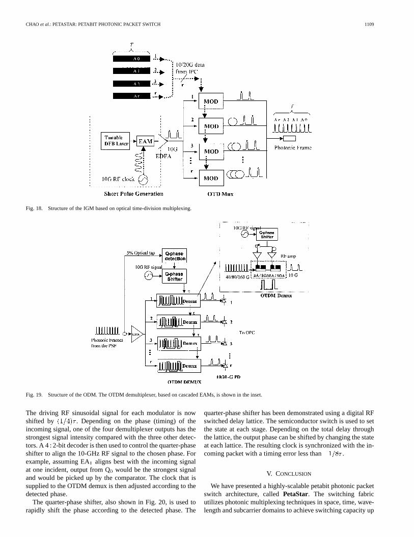
B. OTDM Input Grooming Module (IGM)
Optical time-division multiplexing (OTDM) can operate atultrafast bit rates that are beyond the current electronics limit,which is around 40 Gb/s. By interleaving short optical pulsesat the time domain, aggregated frames can be formed to carrydata at bit rates of hundreds of gigabits per second. Using theOTDM technique, there can be at least one order of magnitudein bandwidth increase compared with the existing electronicsapproach.
The IGM interfaces with parallel electronic inputs from theIPC. Fig. 18 shows the structure of the IGM based on the OTDMtechnology. It consists of a short-pulse generation unit, modu-lator array, and a passive fiber coupler with proper timedelays for time-interleaved multiplexing. Optical pulses withwidths of several picoseconds can be generated using electro-
absorption modulators (EAMs) over-driven by a 10-GHz si-nusoidal clock signal. Using a tunable CW DFB laser as thelight source, the wavelength of the output ultra-short pulses canalso be tunable. The pulse width will be around 7–10 ps gen-erated by the cascaded EAMs, which is suitable for data ratesup to 100 Gb/s. To generate pulses suitable for higher bit rates( 100 Gb/s), nonlinear compression with self-phase modula-tion (SPM) can be used. The pulses, generated from the EAMs,are injected into a nonlinear medium (a dispersion shifted orphotonic bandgap fiber) followed by a compression fiber (dis-persion compensation fiber) to further compress the pulse widthto about 1 ps. The parallelinput lines from the IPC electroni-cally modulate the modulator array to encode the bit stream ontothe optical pulse train. Precise time delays on each branch ofthe fiber coupler ensure time-division multiplexing ofinputs.Through the parallel-to-serial conversion in the multiplexer,cells at 10 Gb/s from the IPC are now effectively compressed inthe time domain as the RZ-type photonic frame that operates at
Gb/s in serial. The fiber coupler and time delays can beintegrated using planar waveguide structures [62].
C. OTDM Output Demultiplexing Module (ODM)
At the receiving end of the system, the ODM demultiplexesphotonic frames from the output of the PSF intoparallel elec-tronic signals at 10 Gb/s. As Fig. 19 shows, the ODM consistsof a quarter-phase detector and quarter-phase shifter, an arrayof OTDM demultiplexers (DEMUX) based on EAMs, and thephoto-detector (PD) array for O/E conversions. We have previ-ously demonstrated ultrafast demultiplexing at 40, 80, 100, and160 Gb/s using cascaded EAMs as the gating device. As shownin the inset of Fig. 19, the OTDM demultiplexer consists of twocascaded EAMs based on multiple quantum well devices [37],[38]. An SOA section is also integrated with the EAM to provideoptical amplification at each stage. The optical transmission ofthe EAM, controlled by the driving electronic signal, respondshighly nonlinearly and produces an ultra-short gating windowin the time domain. Cascading the EAMs can further shortenthe gating window compared with a single EAM. The incomingoptical signal is split by a optical coupler into modula-tors located in the array structure. Each EAM is over-driven bya 10-GHz sinusoidal radio frequency (RF) clock to create thegating window for performing demultiplexing. The RF drivingsignals supplied to adjacent modulators in the array structureare shifted by a time , where is the bit interval inside thephotonic frame. As a result, modulators are able to performdemultiplexing from Gb/s down to 10 Gb/s on consecu-tive time slots of the photonic frame.
The incoming frames may inherit timing jitters induced by ei-ther slow thermal effects (fiber, device, and component thermallengthening) or system timing errors. The result is a slow (com-pared with the bit rate) walk-off from the initial timing (phase).Since the frames are operating on a burst mode, traditional phaselock loop cannot be applied here. To track on the slow varyingjitters on the burst frames, we suggest a quarter-phase lockingscheme using phase detection and a shifter.
A quarter-phase detector is shown in Fig. 20. Four OTDMdemultiplexers, based on EAM technology, are used as thephase detectors because of their high-speed gating capability.
CHAO et al.: PETASTAR: PETABIT PHOTONIC PACKET SWITCH 1109
Fig. 18. Structure of the IGM based on optical time-division multiplexing.
Fig. 19. Structure of the ODM. The OTDM demultiplexer, based on cascaded EAMs, is shown in the inset.
The driving RF sinusoidal signal for each modulator is nowshifted by . Depending on the phase (timing) of theincoming signal, one of the four demultiplexer outputs has thestrongest signal intensity compared with the three other detec-tors. A 4 : 2-bit decoder is then used to control the quarter-phaseshifter to align the 10-GHz RF signal to the chosen phase. Forexample, assuming EAaligns best with the incoming signalat one incident, output from Qwould be the strongest signaland would be picked up by the comparator. The clock that issupplied to the OTDM demux is then adjusted according to thedetected phase.
The quarter-phase shifter, also shown in Fig. 20, is used torapidly shift the phase according to the detected phase. The
quarter-phase shifter has been demonstrated using a digital RFswitched delay lattice. The semiconductor switch is used to setthe state at each stage. Depending on the total delay throughthe lattice, the output phase can be shifted by changing the stateat each lattice. The resulting clock is synchronized with the in-coming packet with a timing error less than .
V. CONCLUSION
We have presented a highly-scalable petabit photonic packetswitch architecture, calledPetaStar. The switching fabricutilizes photonic multiplexing techniques in space, time, wave-length and subcarrier domains to achieve switching capacity up

1110 IEEE JOURNAL ON SELECTED AREAS IN COMMUNICATIONS, VOL. 21, NO. 7, SEPTEMBER 2003
Fig. 20. Quarter-phase detection and rapid RF phase shifter. SW= semiconductor switch.
to petabit/s regime. Packet buffering is implemented electroni-cally at the input and output port controllers to avoid bufferingin the central photonic switching fabric. The result is a buffer-less switch fabric, capable of transporting ultrafast photonicdata frames without E/O conversion. All-optical wavelengthconversion using semiconductor optical amplifier (SOA)and Mach–Zehnder interferometer is used at each stage toenable the cascading of multiple stages of wavelength-to-spaceswitches based on AWG device. A 6400 6400 switchbased on a three-stage Clos network can be realized using 80wavelengths at each switch module while the port speed can beincreased to 160 Gb/s by the OTDM technology, resulting in atotal capacity of 1.024 petabit/s.
To resolve the contention in the three-stage Clos network,we present a new matching scheme, called c-MAC, a concur-rent matching algorithm for Clos-network switches. It is highlydistributed such that the I/O matching and routing-path findingare concurrentlyperformed by scheduling modules. To relaxthe strict arbitration time constraint and round-trip delay be-tween line cards and the packet scheduler and to accommo-date slow-configuration optical switch fabrics, we introduce theconcept of a frame as the basic switching unit in an arbitration(or switching) cycle. A frame aggregates multiple cells that aregoing to the same output from the input lines, allowing suffi-cient time to complete the arbitration and switching operation.The c-MAC scheme provides high throughput with few requiredarbitration steps by maintaining the existing matched pairs be-tween the inputs and outputs so that the number of unmatchedports is drastically reduced at each arbitration cycle. By imple-menting a timer for each head-of-line frame and grating thehighest priority to those ports whose timer expires, the star-vation problem can be eliminated. At the expenses of a mod-erate internal speedup of 1.5, a throughput close to 100% can beachieved under various traffic conditions. A feasible implemen-
tation of the c-MAC scheme, where a crosspoint switch is usedto provide the interconnection between the arbitration modules,is also described.
REFERENCES
[1] R. Callon, “Prediction for the core of the network,”IEEE InternetComput., vol. 4, no. 1, pp. 60–61, Jan./Feb. 2000.
[2] P. Green, “Progress in optical networking,”IEEE Commun. Mag., pp.54–61, Jan. 2000.
[3] G. Vareille, F. Pitel, and J. F. Marcerou, “3 Tbit/s (300�11.6Gbit/s)transmission over 7380 km using C+L band with 25GHz channelspacing and NRZ format,” inProc. Optical Fiber Communication Conf.2001, OFC 2001, vol. 4, La Ville du Bois, France, 2001, p. PD22-1.
[4] K. Fukuchi, T. Kasamatsu, M. Morie, R. Ohhira, T. Ito, K. Sekiya,D. Ogasahara, and T. Ono, “10.92-Tb/s (273/spl times/40-Gb/s)triple-band/ultra-dense WDM optical-repeatered transmission exper-iment,” in Optical Fiber Communication Conf. Exhibit, 2001. OFC2001, vol. 4, 2001, p. PD24-P1-3.
[5] J. A. Baghdadi, A. Safaaijazi, and H. T. Hattori, “Optical fibers with lownonlinearity, and low polarization-mode dispersion for terabit communi-cations,”Optical and Laser Technol., vol. 33, no. 5, pp. 285–291, 2001.
[6] “Cisco 12 000 gigabit switch router,”Cisco Product Document, Sept. 8,1997.
[7] “T-series routing platforms: System and packet forwarding architec-ture,” Juniper Networks. [Online]. Available: http://www.juniper.net.
[8] Avici System, Inc., “The world of terabit switch/router technology,”White Paper, 1997. [Online]. Available: http://www.avici.com/html/white_paper.html.
[9] H. J. Chao, “Saturn, a terabit packet switch using dual round-robin,”IEEE Commun. Mag., vol. 38, pp. 78–84, Dec. 2000.
[10] R. Dettmer, “Photons and petabit for Internet Traffic,”IEE Review, vol.46, no. 4, pp. 16–18, July 2000.
[11] J. E. Smith and F. W. Weingarten, “Research challenges for the next-generation Internet,”Comput. Res. Assoc., May 12–14, 1997.
[12] H. J. Chao, “Next-generation routers,”Proc. IEEE, vol. 90, pp.1518–1558, Sept. 2002.
[13] N. M. McKeown, M. Izzard, A. Mekkittikul, W. Ellerisick, and M.Horowita, “Tiny tera: A packet switch core,”IEEE Micro., pp. 26–33,Jan.–Feb. 1996.
[14] E. Oki, N. Yamanaka, Y. Ohtomo, K. Okazaki, and R. Kawano, “A10-Gb/s(1.25Gb/s� 8) 4�2 0.25mm CMOS/SIMOX ATM switchbased on scalable distributed arbitration,”IEEE J. Solid-State Circuits,vol. 34, pp. 1921–1934, Dec. 1999.

CHAO et al.: PETASTAR: PETABIT PHOTONIC PACKET SWITCH 1111
[15] F. M. Chiussi, J. G. Kneuer, and V. P. Kumar, “Low-cost scalableswitching solutions for broadband networking: The ATLANTA archi-tecture and chipset,”IEEE Commun. Mag., pp. 44–53, Dec. 1997.
[16] E. Oki, Z. Jing, R. Rojas-Cessa, and H. J. Chao, “Concurrent round-robindispatching schemes for clos-network switches,”IEEE/ACM Trans. Net-working, pp. 830–844, Dec. 2002.
[17] Velio Communications Inc., [Online]. Available: http://www.velio.com/product/product_crosspoint.html..
[18] H. J. Chaoet al., “A photonic front-end processor in a WDM ATM mul-ticast switch,”IEEE J. Lightwave Technol., vol. 18, pp. 273–285, Mar.2000.
[19] S. Verma, H. Chaskar, and R. Ravikanth, “Optical burst switching—Aviable solution for Terabit IP backbone,”IEEE NETWORK 2000, vol.14, no. 6, pp. 48–53.
[20] J. S. Tuner, “WDM burst switching for petabit data networks,” inProc.Optical Fiber Communication Conf., vol. 2, 2000, pp. 47–49.
[21] R. Ryf et al., “1296-port MEMS transparent optical cross-connect with2.07 petabit/s switch capacity,” inOptical Fiber Communications Conf., 2001, p. PD22-1.
[22] P. Bernasconi, C. Doerr, C. Dragone, M. Cappuzzo, E. Laskowski, andA. Paunescu, “Large N� N waveguide grating routers,”J. LightwaveTechnol., vol. 18, pp. 985–991, July 2000.
[23] Y. Hida, Y. Hibino, T. Kitoh, Y. Inoue, M. Itoh, T. ShibataSugita, and A.Himeno, “400-channel 25-GHz spacing arrayed-waveguide grating cov-ering a full range of C- and L-bands,” inOptical Fiber CommunicationConf. Exhibit, 2001, vol. 3, 2001, p. WB2-1-3.
[24] K. Takada, M. Abe, T. Shibata, and K. Okamoto, “8�10-GHz-spaced1010-channel tandem AWG filter consisting of one primary and ten sec-ondary AWGs,”IEEE Photon. Technol. Lett., vol. 13, pp. 577–578, June2001.
[25] J. Gripp, P. Bernasconi, C. Chan, K. Sherman, and M. Zirngibl, “Demon-stration of a 1-Tbit packet switch fabric80�12.5G), scalable to 128Tbit (6400�20G),” in Proc. Technical Digest European Conf. OpticalCommunications, ECOC 2000, Germany, 2000, paper: PD2-7.
[26] K. Yamakoshi, K. Nakai, N. Matsuura, E. Oki, R. Kawano, andN. Yamanaka, “5-Tbit/s frame-based ATM switching system using2.5-Gbit/s/spl times/8 optical WDM,” inProc. IEEE Int. Conf. Com-munications, vol. 10, 2001, pp. 3117–3121.
[27] C.-K. Chan, K. L. Sherman, and M. Zirngibl, “A fast 100-channel wave-length-tunable transmitter for optical packet switching,”IEEE Photon.Technol. Lett., vol. 13, pp. 729–731, July 2001.
[28] K. R. Tamura, Y. Inoue, K. Sato, T. Komukai, A. Sugita, and M.Nakazawa, “A discretely tunable mode-locked laser with 32 wave-lengths and 100-GHz channel spacing using an arrayed waveguidegrating,” IEEE Photon. Technol. Lett., vol. 13, pp. 1227–1229, Nov.2001.
[29] R. Ramamurthy and B. Mukherjee, “Fixed-alternate routing and wave-length conversion in wavelength-routed optical networks,”IEEE/ACMTrans. Networking, vol. 10, pp. 351–367, June 2002.
[30] I. Cristiani, V. Degiorgio, L. Socci, F. Carbone, and M. Romagnoli, “Po-larization-insensitive wavelength conversion in a lithium niobate wave-guide by the cascading technique,”IEEE Photon. Technol. Lett., vol. 14,no. 5, pp. 669–671, May 2002.
[31] B. C. Sarker, T. Yoshino, and S. P. Majumder, “All-optical wavelengthconversion based on cross-phase modulation (XPM) in a single-modefiber and a Mach–Zehnder interferometer,”IEEE Photon. Technol. Lett.,vol. 14, pp. 340–342, May 2002.
[32] S. Nakamura, Y. Ueno, and K. Tajima, “168-Gb/s all- optical wave-length conversion with a symmetric-Mach–Zehnder-type switch,”IEEEPhoton. Technol. Lett., vol. 13, pp. 1091–1093, 2001.
[33] J. Leuthold, B. Mikkelsen, G. Raybon, C. H. Joyner, J. L. Pleumeekers,B. I. Miller, K. Dreyer, and R. Behringer, “All-optical wavelengthconversion between 10 and 100 Gb/s with SOA delayed-interferenceconfiguration,”Optical and Quantum Electronic, vol. 33, no. 7–10, pp.939–952, 2001.
[34] H. J. Chao and T. S. Wang, “An optical interconnection network forTerabit IP routers,”IEEE J. Lightwave Technol., vol. 18, pp. 2095–2112,Dec. 2000.
[35] D. K. Hunter, M. H. Nizam, M. C. Chia, I. Andonovic, K. M. Guild,A. Tzanakaki, J. O’Mahony, J. D. Bainbridge, M. F. C. Stephens, R.V. Penty, and I. H. White, “WASPNET: A wavelength switched packetnetwork,” IEEE Commun. Mag., pp. 120–129, Mar. 1999.
[36] K.-L. Deng, R. J. Runser, P. Toliver, I. Glesk, and P. R. Prucnal, “A highlyscalable, rapidly-reconfigurable, multicasting-capable, 100-Gbit/s pho-tonic switched interconnect based upon OTDM technology,”J. Light-wave Technol., vol. 18, no. 12, pp. 1892–1904, 2000.
[37] D. T. K. Tong, K.-L. Deng, B. Mikkelsen, G. Ranbon, K. F. Dreyer, and J.Johnson, “160 Gbit/s clock recovery using electroabsorption modulator-based phase locked loop,”Electron. Lett., vol. 36, pp. 1951–1952, 2000.
[38] K.-L. Deng, D. T. K. Tong, C.-K. Chan, K. F. Dreyer, and J. E. Johnson,“Rapidly reconfigurable optical channel selector using RF digital phaseshifter for ultra-fast OTDM networks,”Electron. Lett., vol. 36, pp.1724–1725, 2000.
[39] L. Tassiulas and A. Ephremides, “Stability properties of constrainedqueueing systems and scheduling for maximum throughput in multihopradio networks,”IEEE Trans. Automat. Contr., vol. 37, no. 2, pp.1936–1949.
[40] N. McKeown, V. Anantharam, and J. Walrand, “Achieving 100%throughput in an input-queued switch,” inProc. IEEE INFOCOM’96,1996, pp. 296–302.
[41] N. McKeown, “ Scheduling algorithms for input-queued cell switches,”Ph.D. dissertation, UC Berkeley, May 1995.
[42] E. Leonardi, M. Mellia, F. Neri, and M. Ajmone, “Bound on averagedelays and queue size averages and variances in input-queued cell-basedswitches,” in Proc. IEEE INFOCOM 2001, Alaska, Apr. 2001, pp.1095–1103.
[43] D. Shah and M. Kopikare, “Delay bounds for approximate maximumweight matching algorithms for input queued switches,” inProc. IEEEINFOCOM 2002, New York, 2002, pp. 1024–1031.
[44] P. Krishna, N. S. Patel, A. Charny, and R. Simcoe, “On the speeduprequired for work-conserving crossbar switches,” inProc. Int. WorkshopQuality of Service’98, May 1998, pp. 225–234.
[45] A. Charny, P. Krishna, N. Patel, and R. Simcoe, “Algorithms for pro-viding bandwidth and delay guarantees in input-buffered crossbars withspeedup,” inProc. Int. Workshop Quality of Service’98, May 1998, pp.235–244.
[46] S. T. Chuang, A. Goel, N. McKeown, and B. Prabhakar, “Matchingoutput queueing with combined input and output queueing,”IEEE J.Select. Areas Commun., vol. 17, no. 6, pp. 1030–1039, Dec. 1999.
[47] I. Stoica and H. Zhang, “Exact emulation of an output queueing switchby a combined input output queueing switch,” inProc. Int. WorkshopQuality of Service’98, May 1998, pp. 218–224.
[48] A. Mekkittikul and N. McKeown, “A practical scheduling algorithm toachieve 100% throughput in input-queued switches,” inProc. IEEE IN-FOCOM 98, vol. 2, Apr. 1998, pp. 792–799.
[49] J. Dai and B. Prabhakar, “The throughput of data switches with andwithout speedup,” inProc. IEEE INFOCOM’2000, Tel-Aviv, Israel,Mar. 2000.
[50] E. Leonardi, M. Mellia, F. Neri, and M. A. Marsan, “On the stabilityof Input-buffer cell switches with speed-up,”IEEE/ACM Trans. Net-working, vol. 9, no. 1, pp. 104–118, Feb. 2001.
[51] L. Tassiulas, “Linear complexity algorithms for maximum throughputin radio networks and input queued switches,” inProc. IEEE IN-FOCOM’98, vol. 2, New York, 1998, pp. 533–539.
[52] T. E. Anderson, S. S. Owicki, J. B. Saxe, and C. P. Thacker, “High speedswitch scheduling for local area networks,”ACM Trans. Comput. Syst.,vol. 11, pp. 319–352, Nov. 1993.
[53] N. McKeown, “The iSLIP scheduling algorithm for input-queuedswitches,” IEEE/ACM Trans. Networking, vol. 7, pp. 188–201, Apr.1999.
[54] Y. Li, S. Panwar, and H. J. Chao, “The dual round- robin matchingswitch with exhaustive service,” inProc. Workshop High-PerformanceSwitching and Routing (HPSR 2002), May 2002, pp. 58–63.
[55] K. Kar, T. V. Lakshman, D. Stiliadis, and L. Tassiulas, “Reduced com-plexity input buffered switches,”Hot Interconnects, vol. 8, 2000.
[56] A. Bianco, M. Franceschinis, S. Ghisoolfi, A. M. Hill, E. Leonardi, F.Neri, and R. Webb, “Frame-based matching algorithms for input-queuedswitches,” inProc. High-Performance Switching and Routing, 2002, pp.69–76.
[57] B. Towles and W. Dally, “Guaranteed scheduling for switches withconfiguration overhead,” inProc. IEEE INFOCOM, vol. 1, June , pp.342–351.
[58] K. I. Kang, K.-L. Deng, S. D. Koehler, I. Glesk, and P. R. Prucnal, “Fab-rication of precision fiber-optic time delays with in situ monitoring forsub-picosecond accuracy,”Applied Optics, vol. 36, p. 2533, 1997.
[59] R. Cole, K. Ost, and S. Schirra, “Edge-coloring bipartite multigraphs inO(ElogD) time,” inProc. Combinatorica 21 (2001), 2001, pp. 5–12.
[60] M. Karol and C.-L. I, “Performance analysis of a growable architecturefor broadband packet (ATM) switching,” inProc. GLOBECOM, Nov.1989, pp. 1173–1180.
[61] K. Eng, M. Karol, and Y. S. Yeh, “A growable packet (ATM) switcharchitecture design principle and applications,” inProc. GLOBECOM,Nov. 1989, pp. 1159–1165.

1112 IEEE JOURNAL ON SELECTED AREAS IN COMMUNICATIONS, VOL. 21, NO. 7, SEPTEMBER 2003
[62] H. Takara, S. Kawanishi, Y. Yamabayashi, Y. K. Tohmori, K. Takiguchi,Y. K. Magari, I. Ogawa, and A. Himeno, “Integrated optical-time divi-sion multiplexer based on planar lightwave circuit,”Electron. Lett., vol.35, no. July, pp. 1263–1264, 1999.
H. Jonathan Chao (F’01) received the B.S. andM.S. degrees in electrical engineering from theNational Chiao Tung University, Hsinchu, Taiwan,R.O.C., and the Ph.D. degree in electrical engi-neering from The Ohio State University, Columbus.
He is a Professor of electrical and computerengineering at Polytechnic University, Brooklyn,NY, where he has been since January 1992. He hasbeen doing research in the areas of terabit IP routers,quality-of-service (QoS) control, optical networkingand switching, and network security. He holds more
than 20 patents and has published over 100 journal and conference papers inthe above areas. He has also served as a Consultant for various companies, suchas Lucent, NEC, and Telcordia. He has been giving short courses to industrypeople in the subjects of SONET/ATM/IP/MPLS networks for over a decade.From 2000 to 2001, he was Cofounder and CTO of Coree Networks, TintonFalls, NJ, where he led a team to implement a multiterabit MPLS switch routerwith carrier-class reliability. From 1985 to 1992, he was a Member of TechnicalStaff at Telcordia, Red Bank, NJ, where he was involved in transport andswitching system architecture designs and ASIC implementations, such as thefirst SONET-like framer chip, ATM layer chip, sequencer chip (the first chiphandling packet scheduling), and ATM switch chip. From 1977 to 1981, hewas a Senior Engineer at the Telecommunication Labs of Taiwan performingcircuit designs for a digital telephone switching system. He coauthored twonetworking booksBroadband Packet Switching Technologies(New York:Wiley, 2001) andQuality of Service Control in High-Speed Networks(NewYork: Wiley, 2001).
Prof. Chao was elected Fellow of the IEEE for his contributions to the ar-chitecture and application of VLSI circuits in high-speed packet networks. Hereceived the Telcordia Excellence Award in 1987. He is a corecipient of the 2001Best Paper Award from the IEEE TRANSACTION ONCIRCUITS AND SYSTEMS FOR
VIDEO TECHNOLOGY. He has served as a Guest Editor for the IEEE JOURNAL
ON SELECTEDAREAS IN COMMUNICATIONS (JSAC) on the special topics of Ad-vances in ATM switching systems for B-ISDN (June 1997), “Next-GenerationIP Switches and Routers” (June 1999), and the recent issue on “High-Perfor-mance Optical/Electronic Switches/Routers for High-Speed Internet.” He alsoserved as an Editor for IEEE/ACM TRANSACTIONS ONNETWORKINGfrom 1997to 2000.
Kung-Li Deng (S’97–M’98) received the B.S. andM.S. degrees in electrical engineering from the Na-tional Taiwan University, Taipei, in 1991 and 1993,respectively, and the Ph.D. in electrical engineeringfrom Princeton University, Princeton, NJ, in 1999.
He is currently the Senior Photonic System Re-search Engineer at General Electric Global ResearchCenter, Niskayuna, NY, working on next-generationpolymer-base platform technology for hybridopto-electronic integration. He is also leading taskson the communication system applications under
General Electric’s photonic advanced technology program. Prior to GeneralElectric, he worked as a Research Assistant Professor at Polytechnic University,Brooklyn, NY. From 2001 to 2002, he was the Chief Scientist and Co-Founderat BeLight Inc., Eaton, NJ, a spin-off startup company from Jedai BroadbandNetworks, Red Bank, NJ, leading the research and development efforts fornext-generation intelligent optical wireless networks. While at Jedai BroadbandNetworks, he was the Senior Research Scientist, a NJ-based startup companyfor next-generation optical access networks. Prior to Jedai, he was a Memberof Technical Staff at Bell Laboratories, Lucent Technologies, Holmdel, NJ,working on 40, 80, 100, and 160-bits/s OTDM systems and next-generationoptical Ethernet technologies. His research interests are in the areas ofoptics and opto-electronics, especially on system-level demonstrations andapplications. He also holds multiple patents in laser ranging, ultrafast opticalsystem and next-generation free-space optical communications systems. Hiscurrent research interests include fiber sensors, advanced optoelectronic pack-aging, next-generation optical Ethernet, photonic packet-switched networks,large-scale interconnection networks, and ultrafast photonic signal processing.
Zhigang Jing (M’01) received the B.S., M.S., andPh.D. degrees from the University of Electronic Sci-ence and Technology of China, in 1993, 1996, and1999, respectively, all in electrical engineering.
He then joined the Department of Electrical Engi-neering, Tsinghua University, Beijing, China, wherehe was a Postdoctoral Fellow. Since March 2000, hehas been with the Department of Electrical and Com-puter Engineering, Polytechnic University, Brooklyn,NY, as a Postdoctoral Fellow. His current research in-terests are highly scalable switch architecture, high-
speed networks, Terabit IP routers, multimedia communication, Internet QoS,Diffserv, MPLS, etc.
Dr. Jing is a Member of the Association for Computing Machinery (ACM).