permission to make digital or hard copies ofall or part
TRANSCRIPT

Copyright © 1992, by the author(s).All rights reserved.
Permission to make digital or hard copies of all or part of this work for personal orclassroom use is granted without fee provided that copies are not made or distributed
for profit or commercial advantage and that copies bear this notice and the full citationon the first page. To copy otherwise, to republish, to post on servers or to redistribute to
lists, requires prior specific permission.

PROGRAMMABLE ARITHMETIC DEVICES FOR
HIGH SPEED DIGITAL SIGNAL PROCESSING
by
Devereaux C. Chen
Memorandum No. UCB/ERL M92/49
14 May 1992

PROGRAMMABLE ARITHMETIC DEVICES FOR
HIGH SPEED DIGITAL SIGNAL PROCESSING
Copyright © 1992
by
Devereaux C. Chen
Memorandum No. UCB/ERL M92/49
14 May 1992
ELECTRONICS RESEARCH LABORATORY
College of EngineeringUniversity of California, Berkeley
94720

Programmable Arithmetic Devices for High Speed DigitalSignal Processing
Devereaux C. Chen
Abstract
The high throughput (computation) requirements of real-time digital signal processing(dsp) systems usually dictate hardware intensive solutions. Often attendant to hardware approachesare problems of high development costs, slow turnaround, susceptibility to errors, and difficultyin testing and debugging, all of which tend to inhibit the rapid implementation of such systems.Research is underway into the synthesis ofapplication specific hardware to aid the system designer byautomatically generating hardware that is "correct by construction". The creation of configurable,pre-fabricated hardware that has been designed for high speed computations forms part of thisresearch and is the main topic of this thesis.
This work contains a survey of some typical real-time dsp algorithms drawn from videoand speech processing and summarizes the particular computation challenges posed by this class ofalgorithms. Currently available hardware choices and their trade-offs and limitations are discussed.Amultiprocessor architecture consisting of programmable arithmetic devices is presented as a novelplatform for supporting high speed digital signal processing. The VLSI realization of the architectureand an accompanying software development environment are presented as a proof of concept. Themain conclusion of this work is that software-configurable hardware approaches to high speed digitalsignal processing problems form viable alternatives to existing approaches, for systems designersinterested in rapidly prototyping or implementing their ideas.
__ s/n(a2-Rabaey
lis Committee Chairman

Dedicated to my loving family,and that wonderful someone who was
"on her way to Dibbidi-dop, early in the morning."

Acknowledgements
No man is an Illajid intire of it selfe;
— J. Donne
I wish to thank my advisor Jan Rabaey for his support and guidance of this
work. His high standards have left an indelible mark upon this thesis. I would also like to
thank Bob Brodersen and Charles Stone for serving on my dissertation committee. Thanks
also to Bob Brayton and John Wawrzynek for participating on my qualifying examinationcommittee,
Among the many members of the U.C. Berkeley eecs faculty who have been
especially encouraging and supportive are David Hodges, Ping Ko, Edward Lee, Richard
Muller, A. Richard Newton, and Aram Thomasian. William Oldham deserves special thanksfor encouraging me to apply to the Department.
Tso-Ping Ma of Yale University, Winston Strachan of St. George's College, and
Sister Margaret Mary of Holy Childhood Prep, represent the many wonderful teachers from
my previous schools who have taught me so much.
Several former colleagues who encouraged and inspired me to continue with graduate studies are Paul Merchant, John Moll, and Chuck Tyler.
Hugo de Man and Francky Catthoor of IMEC gave helpful advice at the beginningof the paddi project.
Participants on the paddi project included Cecilia Yu, who helped with the xilinx
investigation, David Schultz who assisted with the exu layout, Simon Li who assisted with
the scan-test board, and Eric Ng who wrote the paddi assembler and simulator. Their
assistance is gratefully acknowledged. Thanks also to Andy Burstein and Cormac Conroy
for assistance with spice, Angela Cheng, Joan Pendelton and Bart Sano for providing the
pad cells, Chuck Cox for advice on xilinx, Paul Landmann for providing the carry-select
adder cells, Alex Lee for providing the sram cells, and the staff members of the mosis
organization, especially Sam Reynolds, for chip fabrication support.
The bj group members included many fellow students who provided generoustime, support, and camaraderie when it was needed. Special thanks to Alfred Yeung for
being a great office-mate. Staffmembers including Tom Boot, Carole Prank, Sue Mellers,
Brian Richards, Phil Schrupp, Kirk Thege, and Kevin Zimmerman provided the essential
infrastructure which was critical to the success of the project.

Among the many friends who have enrichened my life at Berkeley, Pranav Ashar,
Behzad Behtash, Chedsada Chinrungrueng, Randy Cieslak, German Ferrer, Paul Freiberg,
Bruce Holmer, D.K. Jeong, Ming Lin, Rajeev Murgai, Irena Stanczyk-Ng, Allen Nehorayaff,
Todd Strauss, Greg Thomas, and Greg Uviegara deserve special mention. They, among
many others, have made the going a whole lot easier and fun than it might have been
otherwise.
I am at loss for words to express my gratitude to my parents, Marsden and Viola,
my wife, Sharon, and my cousin Pamela for their wonderful love and encouragement through
the years. This thesis would not have been possible without them. My daughter Kristin
helped make it all a much happier and brighter experience.
To all the people that I should have mentioned but haven't, due to lack of space,
many thanks. Please forgive the omission.
I wouldlike to thank the Hewlett-Packard Company for providing financial support
during my first year as a graduate student.
This project was sponsored by the Defense Advanced Research Projects Agency
(monitored by U.S. Department of Justice, Federal Bureau of Investigation, under contract
no. J-FBI-90-073) and Sharp Microelectronics Technology, Inc. Their support is grate
fully acknowledged. The views and conclusions in this document are those of the authors
and should not be interpreted as representing the official policies, either express ed or im
plied, of the Defense Advanced Research Projects Agency, the U.S. Government, or Sharp
Microelectronics Technology, Inc.

Contents
Acknowledgements i
Table of Contents iii
List of Figures vii
List of Tables x
1 Introduction 11.1 A Perspective 11.2 Goals and Organization 2
2 High Speed Digital Signal Processing 42.1 Introduction 42.2 Video 52.3 Image Processing 62.4 Speech Recognition 72.5 Computation Requirements of High Speed DSP 102.6 Conclusions 12
3 Architectural Classification 133.1 Introduction 133.2 Architectural Taxonomies 14
3.2.1 Flynn 143.2.2 Extensions to Flynn's Taxonomy 143.2.3 Telecommunications ASICs 213.2.4 Image and Video Processing Architectures 223.2.5 Digital Signal Processors 22
3.3 Architectures for High Speed DSP 243.4 Conclusions 26
4 Rapid Prototyping Platforms 274.1 Introduction 274.2 Implementation Platforms 28
in
CONTENTS iv
4.2.1 Programmable DSPs 284.2.2 Generic Components 304.2.3 ASICs 30
4.3 High Level Synthesis 314.3.1 Microsystems: Chip Level 314.3.2 Systems: Board Level 31
4.4 Software-configurable Hardware 324.4.1 Purdue CHiP •. 33
4.4.2 Texas Instrument RIC 344.4.3 CMU White Dwarf 364.4.4 MIT RAP 394.4.5 Video Signal Processors (VSP's) . . . . 40
Philips VSP 41ITT DataWave 42
4.4.6 NTT VSP 454.4.7 Software Reconfigurable Transceiver 454.4.8 Field Programmable Gate Arrays 464.4.9 PADDI: Programmable Arithmetic Devices for High Speed DSP . . 49
4.5 Conclusions 50
5 PADDI: Architectural Design 525.1 Introduction 525.2 Design Goals 535.3 Dynamic/Static and Hardware/Software Interfaces 53
5.3.1 Design Methodology 555.3.2 Functional Design 57
Operator Statistics 59Interconnect Statistics 60Control Statistics 60IO Statistics 66Computation Rate Statistics 66
5.4 Techniques for High Performance 675.5 Processor Architecture 70
5.5.1 Execution Units 70Design Considerations 70Execution Unit Architecture 71
5.5.2 Interconnection Network 74Design Considerations 74Interconnect Network Architecture 75
5.5.3 Control 76Design Considerations 76Control Architecture 77
5.5.4 IO . 825.5.5 Memory 825.5.6 Configuration 82

CONTENTS v
Design Considerations 825.6 Processor Summary 83
5.6.1 Benchmarks 83
5.7 Instruction Set Summary 865.8 Programmer's View 865.9 Summary and Conclusions 86
6 PADDI: Hardware Design 886.1 Introduction 886.2 Execution Unit 89
6.3 Interconnection Network 916.4 Control 98
6.4.1 Nanostore 986.4.2 Branch Logic 100
6.5 Configuration Unit 1046.5.1 Modes of operation 104
Scan Chain 1066.5.2 Finite State Machines 106
6.6 Testability 1096.6.1 Test Modes 109
6.6.2 Test Support System 1106.7 Clocking 112
6.7.1 Layout and Simulation . 1126.7.2 Test Results 115
6.8 Discussion 117
6.9 Conclusions 121
7 PADDI: Software Environment 122
7.1 Introduction 122
7.2 Low-level Programming Tools 1227.2.1 The pas assembler 1237.2.2 The psim simulator 123
7.3 High Level Synthesis for Programmable Arithmetic Devices 1237.3.1 Architectural Constraints 124
7.3.2 Hardware Assignment Using Clustering 125Hierarchical Two Phase Clustering 126Initial Phase 126
Improvement Phase 127Detailed EXU Clustering 127Detailed Quadrant Clustering 128
7.3.3 CADDI Compiler 1297.4 Conclusions 130
8 Conclusions and Future Work 131

CONTENTS vi
A Xilinx Case Study 136A.l Introduction 136
A.2 Limitations of FPGAs 136
B Mapping an Example to PADDI 141
C Programmer's Guide 144C.l Introduction 144
C.l.l Dynamic Instructions 144Registers 145Functions 145
Output Bus Enables 145A and B Register Sources 146Interrupt Enables 146
C.l.2 Configuration Specifiers 147C.1.3 Putting it all Together 147
D Configuration With External Memory 150
E Pin List 152E.l Pad Types 152E.2 PGA Pinout 153
F Assembler Manual Page 156F.l Introduction 156
G Annotated grammar 158G.l Annotated Assembler Grammar 158
H Simulator 162
Bibliography 164

List of Figures
2.1 Pipelined Data Path for Luminance Conversion 62.2 Image Convolution 82.3 Signal Flow Graph of 3x3 Linear Convolver 82.4 Grammar Processor Architecture 11
3.1 Flynn's Taxonomy , 153.2 Flynn's Taxonomy (contd.) 163.3 Skillicorn's Taxonomy 183.4 Basic von Neumann Abstract Machine 193.5 Type I Array Processor 193.6 . Type II Array Processor 203.7 Tightly Coupled Multiprocessor Model • . . 203.8 Loosely Coupled Multiprocessor Model 213.9 Architectural Classification Based on Control/Arithmetic Ratio 233.10 Performance and Flexibility for Different Approaches 24
4.1 Commercial DSP Multiply-Accumulate Time 294.2 SIERA 324.3 Three CHiP Switch Lattice Structures 344.4 Embedding of Graph K4,4 into Switch Lattice 354.5 Texas Instrument's RIC Block Diagram 364.6 CMU's White Dwarf Processor Overview 374.7 White Dwarf Data Path 374.8 White Dwarf Control Flow 384.9 White Dwarf Downloading Flow 394.10 RAP Data Path 404.11 RAP Block Diagram 414.12 Philips VSP 424.13 Philips VSP: ALE Block Diagram 434.14 DataWave: Processor Architecture 434.15 DataWave: Cell Architecture 444.16 NTT VSP Architecture 454.17 XC3000 Logic Cell Array Family 47
vu

LIST OF FIGURES viii
4.18 XC3000 CLB Architecture 47
4.19 XC3000 Combinational Logic Options 484.20 XC3000 Interconnect Structure 48
4.21 PADDI Abstract Architecture 51
5.1 DSI Placement Examples 545.2 Architectural Design Methodology 565.3 General Characteristics of Benchmark Set 585.4 Number of Ops vs. Op Type 595.5 Total Number of Ops vs. Op Type 615.6 Number of Arcs vs. Arc Type 625.7 Total Number of Arcs vs. Arc Type 635.8 Control Structure by Benchmark 645.9 Grammar Processor Control 655.10 IO Statistics 655.11 Computation Rate Statistics 675.12 Computation Rate / IO 685.13 Computation Rate / IO 685.14 Naive Mapping of Uni-processor Task Set 695.15 EXU Architecture 725.16 Primitive PADDI Operations (a) 725.17 Primitive PADDI Operations (b) 735.18 Crossbar Switch 755.19 Nanostore as a Local Decoder 785.20 Four Stage Pipeline 785.21 Local Delayed Branches 795.22 Global Delayed Branches 805.23 Load/Execution Alignment 815.24 PADDI with 32 EXUs 845.25 PADDI with 16 EXUs 845.26 Prototype Architecture 855.27 Prototype Architecture With Multipliers 855.28 System Using PADDI Chips 86
6.1 EXU Architecture 896.2 Logarithmic Shifter 906.3 Register-File Cell , 916.4 EXU Detail 926.5 EXU Critical Path 936.6 Crossbar Network 946.7 Type 1 Bit-slice 946.8 Type 2 Bit-slice 956.9 Layout of Type 2 Bit-slice 956.10 Regenerative PMOS Design 966.11 Regenerative PMOS Design (Spice) 97

LIST OF FIGURES ix
6.12 Interconnect Critical Path 976.13 Interconnect Critical Path Simulation 986.14 SRAM Detail 996.15 SRAM Control Circuitry 1006.16 SRAM Timing Diagram 1016.17 SRAM Read Cycle 1026.18 Branch Logic 1036.19 Clocking of State Latches 1056.20 Section of Configuration Scan Chain 1076.21 FSM1 . . . . 1086.22 PHIM and PHIM Clock Generation / 1086.23 FSM2 1096.24 Test Support System HI6.25 TCB Architecture HI6.26 Clock Distribution 1126.27 Chip Photo 1136.28 Four Quadrant Critical Path 1146.29 25 MHz Counter 1186.30 Simple Low Pass Biquadratic Filter 1186.31 Biquad Processor Schedule 1196.32 Biquad Impulse Response 119
7.1 Software Environment 130
8.1 Processing Power vs. Maximum Signal Frequency 133
A.l Simple Low Pass Biquadratic Filter 137A.2 Transformed Biquad 138A.3 Convolver on XC3090 with Routing Congestion . . . 139A.4 Insufficient Routing Resources for the Convolver 139
B.l Retimed Linear Convolver 142B.2 Linear Convolver Mapping (1/2) 143B.3 Linear Convolver Mapping (2/2) 143
C.l Instruction Format 145
D.l Configuration Timing Diagram 151D.2 Interfacing to External Memory 151
E.l PADDI PGA Pin Assignments 153
H.l Typical Psim Session 163

List of Tables
2.1 Computations and I/O Summary 10
4.1 Application Sample Period 294.2 Instructions per Sample 29
6.1 Chip Characteristics 1206.2 Chip Comparison of Technologies and Areas 120
8.1 Some Typical Dedicated-Function DSPs 132
A.l Comparison of XILINX and PADDI 140
B.l Benchmarks 142
C.l Summary of Arithmetic Instructions 146C.2 Summary of Configuration Specifiers 147
E.l Pad Types 152E.2 PADDI Pin List 154E.3 PADDI Pin List (contd.) 155

Chapter 1
Introduction
A great discovery solves a great problem but there is a grain of discovery in the solution ofany problem. Your problem may bemodest; but ifit challenges your curiosity and brings intoplay your inventive faculties, and if you solve it by your own means, you may experience thetension and enjoy the triumph of discovery. Such experiences at a susceptible age may createa taste for mental work and leave their imprint on mind and character for a lifetime.
— G. Polya, How To Solve It
Weapons are the took of fear; a decent man will avoid them except in thedirest necessity and,if compelled, will use them only with the utmost restraint.
— Lao Tzu Tao Te Ching
1.1 A Perspective
At this point in time, throughout the cad community, and particularly here at
U.C. Berkeley, many resources are being directed to establishing an Integrated System
Design Environment for the rapid design of all levels of electronic systems [29, 12]. The
result will be the creation of efficient, high performance systems which will compete with
present manual design approaches by incorporating the very best of algorithms and by
using advanced implementation technologies. Top priority is being placed on performance
optimization, and reducing the time and cost of implementation.
A particular thrust of this overall cad effort targets high performance real-time
systems. Examples of such systems can be found in the field of digital signal processing
(dsp) which has become a dominant force in signal processing and communications [31].Typical application domains include digital audio [75, 8], speech recognition and synthe
sis [10], mobile communications [44], personal communications systems [14, 47], robotics

CHAPTER 1. INTRODUCTION 2
and electro-mechanical control, digital image and video processing [43], machine vision [11],
digital television [30], high definition television [56], sonar [84], ultrasonic imaging, advanced
video services [27], smart weapons, and advanced fire control for target discrimination and
tracking [71, 76].
In signal processing applications, the computation involves a set of operations
which operate on an infinite data stream (the signal). In many applications, such as facsim
ile, modems, televisions, compact disk players, video cassette recorders, and video cameras,
to name a few, large amounts of data (MB/sec for speech, GB/sec for video) must be
processed in real-time or at the same rate that the data is required. The high speed com
putational requirements of real-time digital signal processing (dsp) systems usually dictate
hardware intensive solutions. Often attendant to hardware approaches are problems of high
development costs, slow turnaround, susceptibility to errors, and difficulty in testing and
debugging. System designers are frequently faced with two main choices, that of using bulky
boards of ttl components or generating theirowncostly application specific integrated cir
cuits (asics). These factors tend to inhibit the rapid and economical implementation ofreal-time systems.
1.2 Goals and Organization
The goal of this work is to enhance the system design environment by defining a
library of ofF-the-shelf macro-components which can be applied to real-time signal process
ing applications. These macro-components should be programmable, support high speed
computation, and possess a high level of integration, With such components, the system en
gineer will be able to synthesize application specific hardware within a veryshort time when
compared to current approaches. This approach can be economical since there are none of
the non-recurring engineering (nre) costs associated with ASIC design and fabrication.
In order to define the contents of the library and the desired programmability and
functionality, algorithms and architectures from real-time speech recognition, image, andvideo processing were examined.
It was observed that most of the systems which perform these algorithms are im
plemented as a set of concurrently operating, bit-sliced, pipelined processors. However the
controller structure,data path composition, memoryorganization, and connection and com
munication patterns of these processors were found to depend heavily upon the particular

CHAPTER 1. INTRODUCTION 3
application. The challenge is to define a restricted set of programmable components thatcovers these apparently dissimilar architectures. Four classes of devices are necessary: controllers, memory (including delay lines), data path blocks, and interprocessor communica
tion units. Fairly efficient solutions are available for control structures (using programmablelogic devices or plds) and memory structures (using commercially available memory). However, no high-level re-programmable data path or interprocessor communication structures
are yet available. The creation of such configurable, pre-fabricated hardware, designed forhigh speed computations, is the main topic of this thesis.
The rest of the thesis is organized as follows: Chapter 2 examines typical exam
ples of some real-time applications, and summarizes their computation requirements and
common architectural features. Chapter 3 discusses ways of differentiating between the
many architectural styles found in DSP and focuses on one particularly suited to high speed
DSP, and which is based on control/arithmetic ratio. A review of currently available im
plementation approaches for these computation intensive applications, together with their
trade-offs and limitations, is presented in Chapter 4. The need for rapid prototyping of
systems in general and high speed dsp data paths in particular, and the benefits of using
software-configurable hardware for rapid prototyping is also discussed. The main goal of
this research was to develop a programmable architecture for the rapid prototyping of high
speed dsp data paths. Such an architectureis presented in Chapter 5. It consists of clusters
of multiple programmable arithmetic devices orexecution units (exus) connected by a flex
ible communication network for data and status flags, with wide inter-exu and inter-cluster
communication bandwidth. In order to demonstrate concept feasibility, a prototype chip,
dubbed PADDI for Programmable Arithmetic Devices for Digital Signal Processing, was
designed and fabricated [25]. Its VLSI implementation is described in Chapter 6. The sup
porting software environment necessary to program these devices is discussed in Chapter 7
along with compilation approaches, and Chapter 8 concludes the dissertation.

Chapter 2
High Speed Digital Signal
Processing
Fallacy: There is such a thing as a typical program.Pitfall: Designing an architecture on the basis of small benchmarks or large benchmarks froma restricted application domain when the machine is intended to be general purpose.
— J. Hennessy and D. Patterson, Computer Architecture A Quantitative Approach
2.1 Introduction
In this chapter we will examine several representative real-time DSP applications,
in order to ascertain their computation requirements. While there exist many different ar
chitectural approaches for implementing real-time DSP algorithms, the hard-wired pipelined
data path approach is particularly efficient because each algorithm can be hard-wired into
it's own unique data path. In short, the data path is "tailor-made" to fit the algorithm.This approach has been widely and successfully applied.
As each application is discussed, we will present several example architectures
which illustrates the pipelined data path approach. The basic architectural features such
as level of pipelining, functional requirements, control, and i/o bandwidth of each examplewill be examined.

CHAPTER 2. HIGH SPEED DIGITAL SIGNAL PROCESSING 5
2.2 Video
High definition television, or hdtv, is rapidly on its way to becoming a commer
cial reality [53]. Let us consider a typical HDTV bit transfer rate. Given a typical frameof 900x1200 pixels, a display rate of 30 frames/sec, with each pixel composed of 16bits (8luminance, 8 down-sampled chrominance) or 24 bits RGB the resulting transfer bit rate is
900 x 1200x 30 x 24 or approximately 800 Mbit/sec or 100 MB/sec. Typical signal process
ing requirements are yuv and RGB conversions, digital filtering, video compression, motion
compensation, and sampling conversion [85]. If one makes the reasonable assumption that
any of these algorithms can require several tens of operations, then the resulting computa
tional requirements are in the billions of (byte) operations per second (gops). For higher
resolution screens and/or more complicated algorithms, this can increase by one or two
orders of magnitude.
As anexample, consider the conversion of RGB to YUV [88]. Video sources generate
three color signals, red (R), green (G), and blue (B). The three color signals are oversampled
to 27 MHz and converted to eight bits. These signals are often converted to luminance (Y),
and two chrominance (U,V) signals for further processing. This conversion is done by a
video matrix according to the following three equations:
y _ 77 *R+150 *G+29 *B
U =
256
-44* R--87*G+131 *B
256
131* R-•110*(?--21 *BV =
256
In [88], various hard-wired data paths were constructed in an attempt to meet the
high throughput requirements. Pipelining was found necessary to meet the the clocking rate
specification. Fig. 2.1 shows a possible data path to perform the luminance conversion. It is
composed of a set of pipelined carry save full-adders (csfas), which performs the luminance
conversion. The final stage is a pipelined vector merging adder (vma). In the luminance
calculation, ten additions and ten shifts are performed at a rate of 27 MHz., which amounts
to a total computational requirement of 540 mops. If one also takes into account the oper
ations required for the two chrominance calculations, the total computational requirement

CHAPTER 2. HIGH SPEED DIGITAL SIGNAL PROCESSING
C C
RS
F
S
F
A A LattJ
^15^1
c U c C C
s s—i
s S
F F F F
A
AA A A tAJ
Figure 2.1: Pipelined Data Path for Luminance Conversion
is 1,674 mops. Salient architectural features include the use of many fast operational units,
and the heavy reliance on pipelining to meet the computational requirements. Additionally,
minimal control logic is required because of the highly pipelined nature of the design. The
data input streams are 8b wide and the output streams are 16 wide. Therefore 213 MB/sec
of i/o bandwidth are required for the RGB and YUV signals, excluding and synchronizationsignals.
Flexible memory address generators are also required in video processing. A flex
ible memory control chip for formatting data into blocks suitable for video coding appli
cations is described in [106]. In this case, fast programmable counters are used to effect
the address generation while data path pipelines are used to format the data according tospecification.
2.3 Image Processing
The computational needs of image processing will vary depending on the level of
the processing being done, and the spatial and temporal resolution required. The com
putational requirements of low level image processing are quite high, especially if done in
real-time. The motivations of performing the processing in real-time are discussed in [104].

CHAPTER 2. HIGH SPEED DIGITAL SIGNAL PROCESSING 7
A real-time image processing chip set is described in [104, 103]. The functions performed
by these chips are 3x3 convolution, 7x7 logical convolution, 3x3 non-linear filtering basedon sorting, image contour extraction, feature extraction, and line delays. Chips of these
types are in commercial production [72].
As an example, consider the 3x3 linear convolver. A mask of fixed coefficients
is dragged across an image (Fig. 2.2). At each point, the output y(ij) is the sum of
the products of the coefficients and their corresponding pixel intensities. A signal flow
graph, (sfg), of the computation is shown in Fig. 2.3. In a real-time implementation of
this algorithm (where a new result might be required every clock cycle), high throughput
is best achieved by using multiple data path pipelines (composed of shifters and adders
in this example since the coefficients are fixed), interconnected in a way to reflect the
algorithmic data flow. The sfg can be hard-wired into the architecture by mapping it
directly to hardware. In the convolution, eight additions and nine shifts are performed
at a rate of 10 MHz., which amounts to a total computational requirement of 170 mops.
As in the RGB to yuv converter example, salient architectural features include the use on
many fast operational units, and the heavy reliance on pipelining to meet the computational
requirements,. The control logic requirements are minimal because of the highly pipelined
nature of the design. The data i/o streams are 8b wide and require 20 MB/sec of i/o
bandwidth excluding any synchronization signals. (The actual architecture used in [104]
was a pipelined data path composed of multiply accumulate units with a somewhat different
topology than the sfg).
2.4 Speech Recognition
The computational requirements of speech recognition will vary depending on the
type of recognition being performed (isolated word vs. connected speech), whether it is
speaker dependent or independent, the size of the vocabulary being supported, and the type
of algorithm being used. The computational needs are exacerbated when the recognition
is performed in real-time. A real-time isolated-word speech recognition system with a
vocabulary of 1000 words was presented in [58]. It requires the computation of 1.25 M
equations/sec or roughly 60 mips, where each equation is a dynamic programming recursion
equation.
The 3000 word, real-ime, hidden Markov model-based, continuous-speech recogni-
CHAPTER 2. HIGH SPEED DIGITAL SIGNAL PROCESSING
IMAGE
X XXX XXX
x xjx x x~|xlx
x xjx X x iX X
X X ; X X x i X X
X X X X X X X
X X X X X X X
X X X X X X X
•
MASK
all •12 •13
•21 •22 •23
•31 •32 •33
y(ij)= 2 2 a(m,n)x(i-m+2,j-n+2)m=l 1=1
Figure 2.2: Image Convolution
© ADO [J D8LAY ©»-
_E
FEATURES:
algorithm is rabd.wibxo
high performance via
pipelining, parallel units
no sesouscb sharing
simple ofebatobi
sfborc communication
SMHJS CONTROL
1 P 1 'D 1
RESULT
m
Figure 2.3: Signal Flow Graph of 3x3 Linear Convolver

CHAPTER 2. HIGH SPEED DIGITAL SIGNAL PROCESSING 9
tion system described in [97] is another example. The word processing sub-system performsaViterbi search over 50,000 states and computes 225 Mops/sec with 85 MB/sec ofmemoryaccesses [116]. Speech recognition accuracy is further enhanced when syntactic constraintsare imposed on the concatenation of individual words in the vocabulary. This task is performed in the grammar processing sub-system which searches for the most probable wordsequence given transition probabilities in speech model supported. The grammar process
ing sub-system performs evaluations of the starting word probabilities associated with the
across-word transitions and computes 200 Mops/sec with i/o bandwidth of 265 MB/sec.Recently, this system has been upgraded to handle 60,000 words in real-time with 30 ac
cesses per state which require in excess of 600 MB/sec of i/o bandwidth [115]. In thissystem, 520 Mops/sec are required.
Let us discuss thegrammar processing sub-system in some more detail ( [22]). Thestatistical grammar model allows any word to follow any other word. Associated with the
ith. word produced bytheword processing sub-system is a probability PGO{, the probabilitythat the word i ends at a particular point in time. The grammar sub-system calculates a
probability PGIj, the probability that word j starts in the next frame. This jth successor
word probability is then sent back to the word processing sub-system. The probability
PGlf(t +1) under the statistical grammar model is found by using:
PGlf(t+1) = max [PGOi(t) x cy] (2.1)
where c,j is the transition probability from word i to word j. The evaluation of the ith word
(equation (2.1)) is terminated when the probability falls below a programmable threshold
and processing, and the i + 1thevaluation is begun. Assuming average of 17 successors per
word ( [22]), the two cycle branch delay of the Grammar Processor leads to a 12 per centperformance branch penalty. The dynamically adjusted threshold will terminate successor
updates before complete processing of all the successors of a word. It is not unreasonable
to.assume cases where fewer than 8 successors are updated per word. In these cases, the
performance branch penalty becomes 25 percent or more. If the branch delay penalty were
four cycles instead of two, these cases would suffer a performance branch penalty of 50 percent ormore. Clearly in this andotherapplications which contain repetitive data-dependent
loop iterations, low overhead conditional branching between the loop iterations is desirable
for efficient hardware utilization. Fig. 2.4 shows adetailed block diagram of the architecture
of the Grammar Processor which is one of two processors in the Grammar Processing sub-

CHAPTER 2. HIGH SPEED DIGITAL SIGNAL PROCESSING
YUV
CONV.
3x3
CONV.
WORD
PROC.
GRAMMAR
PROC.
MOPS 1674 170 225/520 200
IO (MB/sec) 213 20 85/600 265
10
Table 2.1: Computations and I/O Summary
system ( [22]). The main architectural features are: 1) the algorithm is hard-wired into the
data paths 2) high performance is achieved through extensive pipelining and parallelism 3)
operators are very simple (add and compare/select) 4) irregular communication patterns,
among operators. 5) high i/o bandwidth is necessary 6) low overhead branching between
loop iterations.
The main architectural features of the Grammar Processor are very similar to
the previously discussed video and image processing examples. It is also useful to note
that in those,examples the communication patterns between the various operational units
was regular whereas here they are rather irregular. There, the word length requirements
were fixed, 8b and 10b respectively, whereas here they vary between 12b and 19b. The
previous exampleswere fully pipelined, whereas here the address generation unit is hardware
multiplexed. There the i/o bandwidth requirements are not as high as here. Here, fast,
data-dependent branching is required for terminating the calculation for a given word when
the probability falls below its threshold.
2.5 Computation Requirements of High Speed DSP
Table 2.1 summarizes the computational and i/o requirements of some of the
examples presented in the previous section. From these numbers we can see that real
time DSP applications place a tremendous demand on both computation and bandwidth
requirements.
Such high speed computation is required in video and real-time image processing
because of the high throughput requirements. In speech, high speed computation is also
required, because, although the sampling rate is lower than for video, the algorithms aretypically more complex.
The goal of this work is to define a set of high level, programmable macro-

CHAPTER 2. HIGH SPEED DIGITAL SIGNAL PROCESSING
IS
\Z7OPERATOR
SUCCESSOR
UPDATE
UNIT
I REGISTER x s MUX
FEATURES:
ALGORITHM HARD-WIRED
HIGH PERFORMANCE VIA
PIPELINING, PARALLEL UNITS
LOW RESOURCE SHARING
SIMPLE OPERATORS
IRREGULAR COMMUNICATION
WIDE I/O BW
VARIOUS WORD LENGTHS
SIMPLE CONTROL
S.^3fcBEXT
MEM*•—< I/O START
FIPOEMPTY
Figure 2.4: Grammar Processor Architecture
11
12
(STATE)

CHAPTER 2. HIGH SPEED DIGITAL SIGNAL PROCESSING 12
components to support the rapid prototyping of real-time dsp data paths. Case studies
of real-time algorithms and pipelined data path architectures such as discussed above, en
able us to identify the following key architectural features which must be supported by these
macro-components:
a) a set of concurrently operating execution units (exvs) with fast arithmetic, to
satisfy the high computational (hundreds ofuo?s) requirements.
b) very flexible communication between the exvs to support the mapping of a
wide range of algorithms and to ensure conflict free data routing for efficient hardwareutilization.
c) support for moderate (1-10) hardware multiplexing on the EXUs, for fast computation of tight inner loops.
d) support for low overhead branching between loop iterations.
e) wide instruction bandwidth.
f) wide i/o bandwidth (hundreds of MB/sec).
2.6 Conclusions
In this chapter it has been shown that high speed DSP applications, particularly
real-time ones, require massive amounts of computation and wide i/o bandwidth. Practi
cal implementations of these high speed systems usually require the creation of application
specific hardware. Although many different architectural styles exist, pipelined hard-wired
data paths, tuned to reflect the data-flow of the algorithm, result in particularly efficient
system implementations. The goal of this work is to define asetofhigh level, programmable
macro-components to support the rapid prototyping of such data paths. The key compu
tational requirements and architectural features that should be supported by these macro-
components were identified by surveying a variety of existing data paths.

Chapter 3
Architectural Classification
"A good classification scheme should reveal why a particular architecture is likely to providea performance improvementn
— David Skillicorn, A Taxonomy for Computer Architectures
3.1 Introduction
There are many reasons for classifying architectures. One is historical i.e. un
derstanding past accomplishments. Another is the identification of missing gaps i.e. the
revelation of configurations that might not otherwise have occurred to a system designer.
Another is that it allows useful performance models to be built and used. A good classifica
tion scheme should reveal why a particular architecture is likely to provide a performance
improvement [111].
In this chapter we will investigate ways of differentiating between the many ar
chitectural styles found in DSP. In order to establish a framework we will first consider
taxonomies for general purpose computer architectures. We will also consider more spe
cialized ones for ic applications such as telecommunications and image processing. We will
then focus on a classification developed specifically for DSP architectures. It is based on the
concept of control/arithmetic ratio which is related to the amount of operation sharing on
an arithmetic unit. This taxonomy is particularly suitable because of the strong empha
sis on high speed computations in real-time dsp. Using this taxonomy we will investigate
what are the most viable architectural approaches for satisfying the key computation re
quirements of high speed dsp. The answer has already been hinted at in Chapter 2 where
it was shown that hard-wired pipelined data path architectures were well matched to the
13

CHAPTER 3. ARCHITECTURAL CLASSIFICATION 14
computational requirements of real-time dsp. We will compare the various architectural
styles for functionality, performance, and hardware implementability.
3.2 Architectural Taxonomies
The conceptsof instruction streamparallelism, data stream parallelism, nodegran
ularity, and control/arithmetic ratio are relevant when making architectural comparisons.
They are discussed below in several different taxonomies.
3.2.1 Flynn
The classical taxonomy for computer systems was presented by Flynn in [37, 38].
The classification (Fig. 3.1 and Fig. 3.2) is based on the parallelism within the instruc
tion stream and parallelism within the data stream. Flynn observed that the methods for
achieving parallel operation depended on replicating the instruction stream and the data
stream. This gives rise to four classes of computers: single-instruction single-data (sisd),
single-instruction multiple-data (simd), multiple-instruction single-data (misd), multiple-
instruction multiple-data (mimd). A sisd computer is essentially a serial computer. A simd
computer is essentially a vector processor. A misd computer is generally unrealistic for
parallel computation while a MIMD computer is the most general. The two most interesting
types for achieving high performance through parallelism of operation are simd and MIMD
[117].
3.2.2 Extensions to Flynn's Taxonomy
Since Flynn's original work there have been many suggestions on how to modifyand/or extend it. The work by Skillicorn [111] is one such example. The classificationmethod is shown if Fig. 3.3. At the highest level, the model of computation is consid
ered, for example, von Neumann, dataflow, and graph reduction models. At the next level,
the abstract machine captures the essence of a particular architecture form without dis
tinguishing between different technologies and implementations. In this classification, the
basic functional units are instruction processors (for instruction interpretation i.e. if theyexist in the model), data processors, memory hierarchy, and a switch that provides connec
tivity between other functional units. The basic von Neumann abstract machine is shown

CHAPTER 3. ARCHITECTURAL CLASSIFICATION
Control
Unit
I-stream
Arithmetic
Processor
Data-stream
Model of an SISD computer
I-stream
Arithmetic
Processor
Data-stream
Arithmetic
Processor
Data-stream
Control
Unit
•
O
Arithmetic
Processor
Data-stream
Model of an SIMD computer
Figure 3.1: Flynn's Taxonomy
15

CHAPTER 3. ARCHITECTURAL CLASSIFICATION
Control
Unit
I-streamlYj
Arithmetic
Processor
I-stream2
p
Control
Unit
Arithmetic
Processor
Data-stream
I-streamN
O
•
•
•
Control
Unit
Arithmetic
Processory
Modelofan MISD computer
Control
Unit
I-streamlk
Arithmetic
Processor
Data-streaml
I-stream2
P
Control
Unit
Arithmetic
Processor
Data-stream2
I-streamN
P
•
•
•
•
Control
Unit
Arithmetic
Processor
Data-streamNP
Modelof an MIMD computer
Figure 3.2: Flynn's Taxonomy (contd.)
16

CHAPTER 3. ARCHITECTURAL CLASSIFICATION 17
in Fig. 3.4 as an example. The next level is the machine implementation which could be,for example, the architecture as seen by the assembly language programmer, as well as thetechnology used.
A series of states can be associated with the internal structure of each processingunit in the abstract machine. Skillicorn accounts for the three major ways to increase performance. The first is to re-arrange the internal states to increase parallelism by removingany unnecessary sequentiality in the state transition sequence. The second is to pipeline the
state transitions, with the recognition that pipelining will complicate certain instructions.
The third is to replicate functional units. The author presents several models which contain
functional unit replication: two types of array processors, and tightly and loosely coupledmultiprocessors.
The basic paradigm of the array processors is similar to the simd model of Flynn,
but further distinctions are drawn depending onthe interconnectivity of the units. A type I
arrayprocessor model is shownin Fig. 3.5. Here the data processor-data memory connection
is n-to-n and the data processor-data processor connection is n-by-n. (In an n-to-n switch
connection, the ith unit of one set of functional units connects to the ith unit of another.
This type of switch is a 1-to-l connection replicated n times. In an n-by-n switch connection,
each device of one set of functional units can communicate with any device of a second set
and vice versa. In a 1-to-n switch connection, one functional unit connects to all n devices of
another set of functional units.) A type II array processor model is shown in Fig. 3.6. Here
the data processor-data memory connection is n-by-n and there is no connection between
the data processors.
The basic paradigm of the multiprocessors is similar to the MIMD model of Flynn,
but again, further distinctions are drawn depending on the interconnectivity of the units.
A tightly coupled multiprocessor model is shown in Fig. 3.7. Both data and instruction
processors are replicated, but the data processors share a common data memory. Com
munication and synchronization between processes is achieved by used of shared variables.
There is an n-by-n switch between data processors and data memories. Loosely coupled
systems also have functional unit replication. The connection between data processors and
data memories is n-to-n, and there is an n-by-n connection between the data processors. A
loosely coupled multiprocessor abstract machine is shown in Fig. 3.8.
Another classification is contained in the paper by Seitz [110] which presents a
useful taxonomy for concurrent VLSI architectures that adhere to a basic structural model

CHAPTER 3. ARCHITECTURAL CLASSIFICATION
Model of computation
Abstract machine model
No. of instruction processorsNo. of data processorsconnection structure
Performance model
simple or pipelinedstate diagram
Implementation model
implementation technologyspeed
Figure 3.3: Skillicorn's Taxonomy
18

CHAPTER 3. ARCHITECTURAL CLASSIFICATION
Instructions
Stale
Operands Instructions
Figure 3.4: Basic von Neumann Abstract Machine
NxN
Figure 3.5: Type I Array Processor
Addresses
Instruction
Memory
Hierarchy
Instruction
Memory
Hierarchy
19

CHAPTER 3. ARCHITECTURAL CLASSIFICATION
NxN
Figure 3.6: Type II Array Processor
NxN
Figure 3.7: Tightly Coupled Multiprocessor Model
Instruction
Memory
Hierarchy
Instruction
Memory
Hierarchy
20

CHAPTER 3. ARCHITECTURAL CLASSIFICATION
NxN
Data
Memory
Hierarchy
Instruction
Memory
Hierarchy
21
Figure 3.8: Loosely Coupled Multiprocessor Model
based on the repetition of regularly connected elements. Based on the complexity (or
granularity) of the nodes (or computing elements) i.e. the node granularity, the author
identifies five major classes i.e. rams, logic enhanced memories, computational arrays,
microcomputer arrays, and conventional computers, in increasing order of node complexity.
The classes defined span a broad range of computational elements.
3.2.3 Telecommunications ASICs
In the paper by Keutzer [59]. the scope of the taxonomy is restricted to ic appli
cations and architectures, specifically: microprocessors, digital signal processors, floating
point units, co-processors such as for graphics and memory management, protocol engines
for communications applications, sequencers, and glue logic.
The author analyzed over one hundred ASIC designs for telecommunications ap
plications, implemented in standard cells. He found that these ASICs tended to be control
dominated, with little need for arithmetic, typically requiring low component density (under
10,000 logic transistors), and operating below 10 MHz.

CHAPTER 3. ARCHITECTURAL CLASSIFICATION 22
3.2.4 Image and Video Processing Architectures
The idea of node granularity is used in the classification of over forty image pro
cessing LSis made in Japan in the 1980's [41]. The author classifies the devices into five
categories: the fully parallel processor (fpp), the partially parallel processor (ppp), the dig
ital signal processor (dsp) specialized for image processing, the functional processor (fp),
and the neural network processor (nnp). In this taxonomy, fpps correspond to arrays of
very fine-grained, lb ALUs, operating in simd fashion to form so-called Cellular Array Pro
cessors. The author lists four FPP-like devices. Eleven PPP-like devices are listed, ppps
are chips which contain several pipelined processing elements. A processing element might
contain an 8b ALU and an 8x8 multiplier for example. Image processing dsps essentially
contain one large-grained processor containingj for.example, a 16b ALU, 16bxl6b multiplier,
and one 16b accumulator. The processors are designed to handle specific operations such
as spatial convolution, FIR filtering, and Discrete Cosine Transforms (dct). Eight DSP-like
devices are listed, fps are essentially asics that perform specific task such as address con
trol, feature extraction, character recognition. Thirteen of these devices are listed. Four
NNPs are listed for tasks such as character, text, voice, and image recognition.
Similar classes of image processing ics as above are produced elsewhere e.g. [72],to name just one.
Another interesting classification for real time video architectures is contained
in [126], where the author attempts a functional classification based on processing properties, memory properties, communication properties, and control properties. Examples ofdifferent video architectures are presented: a) systolic arrays b) wavefront arrays c) self-timed language-driven architectures [125]. Specific chips are discussed: a) the NEC vspmsystem [121] b) the Matsushita ISMP chip [73] c) the Philips vsp chip [127] The roughtrade-ofFs of asynchronous vs synchronous schemes are mentioned.
3.2.5 Digital Signal Processors
Ageneral classification for dsp architectures, based onthecontrol/arithmetic ratio,was suggested by Brodersen and Rabaey [15]. It is based on the amount of operationsharing on an arithmetic unit (hardware multiplexing), a concept developed further in [20].We will adopt this taxonomy since the concepts of control/arithmetic ratio and hardwaremultiplexing are closely related to the issue of high speed dsp computation which is our

CHAPTER 3. ARCHITECTURAL CLASSIFICATION
CONTROLFLOW
DRIVEN
A
DSP ARCHITECTURES
MiGro-Proccuor
GcnenlPoipoae Signal Processor
DedicatedSignalProcessor
Dedicated Malti-Proccifors
Data Path Oustera
Bit-Serial
Systolic VDATAFLOW
DRIVEN
Figure 3.9: Architectural Classification Based on Control/Arithmetic Ratio
23
main interest. This classification does not explicitly consider node granularity. However, it
is included implicitly since it is closely related to the control/arithmetic ratio, as is apparent
in Fig. 3.9.
The authors in [15] explained their classification as follows:
Architectures can be classified in many different ways. One way of classificationis based on the amount of operation sharing on an arithmetic unit, as shown inFig. 3.9. One extreme end of the scale represents the traditional micro-processorarchitecture, where all arithmetic operations are time-multiplexed on one singlegeneral purpose ALU. This architecture is classified as control driven, sincethe functionality of the programmed device is completely determined by the contents of the control section. On the other end of the spectrum, one can findarchitectures such as systolic arrays (bit-parallel or bit-serial), where each operation is represented by a separate hardware unit. The architectures are calledhard-wired or data-flow and the control section is minimal, if at all existing.Naturally, a complete suite of in-between architectures can be defined. In fact,one of the major challenges in architectural design is to strike the right balance between control and data path sections for a given application and a giventhroughput range.
Henceforth, we will assume that the reader is reasonably familiar with the different
classes outlined in Fig. 3.9 i.e. bit-serial, systolic, data path clusters, dedicated multi
processors, dedicated signal processors, general purpose signal processors, micro-processors.

CHAPTER 3. ARCHITECTURAL CLASSIFICATION
FULLY
HARDWIREDINTERMEDIATE
ASSEMBLY
CODE
Data Path Clusters
Bit-Serial
Systolic
Dedicated DSP
Dedicated
Multi-Processors
Micro-Processor
General Purpose
Signal Processor
< PERFORMANCE
FLEXIBILITY
Figure 3.10: Performance and Flexibility for Different Approaches
Reference should be made to [15] for any necessary clarification.
>
24
3.3 Architectures for High Speed DSP
What architectural approaches satisfy the specific computation requirements of
high speed dsp, that were outlined in Section 2.5 of Chapter 2?
For a given algorithm, hard-wired approaches usually dominate in performance
since they can bedesigned to fit thespecific problem athand (with thecaveat thatasuperioralgorithm in software can beat an inferior algorithm in hardware). Furthermore, hard-wiredapproaches are more efficient since they tend not have any of the extraneousness (such asunused hardware units) thatageneral purpose programmable processor might have. Control
driven architectures are easily prototyped since can be solved by software e.g. programminga general purpose DSP. Software systems are more easily created and simulated than hard
wired approaches which require the creation of application specific hardware. The problemofrapid prototyping for high speed dsp applications poses the interesting challenge offindingarchitectural approaches which exhibit the flexibility of control driven ones and the highperformance of hard-wired ones.
(Fig. 3.10) shows therough trade-offs inperformance and flexibility for the different

CHAPTER 3. ARCHITECTURAL CLASSIFICATION 25
architectural classes ofbased on the control/arithmetic taxonomy. Digital signal processingchips are now capable of tens of millions of multiply-accumulates per second. However,they are still not fast enough to meet the computations intensive tasks of real-time dsp.
Section 4.2.1 will discuss these processors further. Bit-serial architectures do not lend
themselves easily to hardware multiplexing and conditional operations which limits theirapplication range. For high performance circuits, they are less area efficient and are slower
than bit-parallel ones for the reasons outlined in [54]. Systolic architectures ( [62, 63])are generally restricted to algorithms which can be formulated in a regular fashion (suchas filters). Examples of bit-serial, systolic, and semi-systolic programmable filters can befound in [86, 55, 50].
Vector-pipelined architectures such as described in [123] (not classified in [15])can achieve high throughput rates. However, due to the high branching penalty overhead
associated with very deep pipelines, the use of conditional operations is very restricted.
There have been recent investigations to alleviate this overhead [33], but this is still in theresearch phase.
Moderate performance has been reported for architectures which have dedicated
multi-processors. The control based nature of these architectures restricts the throughput
range. In general, the performance of architectures with a restricted number of large gran
ularity processing elements (as constrained by chip area say) can be improved by increasing
the level of pipelining of the processors e.g [127]. However conditional operations will have
severe overhead penalties due to the deep pipelines.
On the topic of heterogeneous data path clusters, the authors in [15] stated:
The control oriented processor approach tends to break down for applicationswith higher throughput ranges (such as required in speech recognition, video,and image processing), since the ratio between data rate and instruction ratetends to approach unity in these cases. A multi-data path approach with limitedhardware sharing (and hence small control unit) and extensive use of pipeliningand concurrency is required.
Detailed examples of data path clusters or hard-wired data paths were presented
in Chapter 2. The distinguishing features of the hard-wired data path approach are the
high computational speeds and hardware efficiency achievable through the use of heavy
pipelining and concurrency and the "hard-wiring" of the algorithms into the data paths. In
cases where conditional operations are required, these can often be hard-wired into the data

CHAPTER 3. ARCHITECTURAL CLASSIFICATION 26
path with little or no overhead. The operational units will be specified by the computation
nodes of the algorithm, and will have very little unnecessary overhead. As a consequence
of better hardware efficiency, hardware replication becomes feasible. Hardware replication
can increase concurrency and performance, and can be used together with or instead of
pipelining as appropriate.
3.4 Conclusions
Several architectural taxonomies were discussed. Focus was placed on a scheme
which uses the control/arithmetic ratio to distinguish between different dsp architectures.
Using this scheme, architectural styles were compared for functionality, performance, and
hardware implementability. It was shown that among the approaches to achieving high
performance, hard-wired pipelined data paths have distinct advantages over control ori
ented processor approaches, since the ratio between data rate and instruction rate tends to
approach unity in these cases.

Chapter 4
Rapid Prototyping Platforms
"A wide variety of chips move to higher levels of integration, making previous distinctionsambiguous and heralding a. new generation of DSP technology",
— W Andrews, Computer Design Magazine [7]
4.1 Introduction
In real-time dsp applications the emphasis is on performance. Because of their
distinctive advantages in achieving high performance, hard-wired pipelined data paths are
used in many designs (Chapters 2 and 3). Currently, these data paths are implemented as
ASIC s. The costs in money and time to design, fabricate, test, and debug these integrated
circuits are usually non-trivial.
In order to capture market share for any product, a quick time to market can be
critical, more so due to increasingly shorter and shorter product life cycles. Engineers need
to be able to rapidly implement, test, and modify their designs. In short, a capability for
rapid prototyping is needed.
The goal of this work is to define software-configurable integrated circuits which
can be used to synthesize hard-wired pipelined data paths. Since the configuration of
the hardware is done in software, it is quickly and easily changed which makes it ideal
for rapid prototyping, and, because the hardware can be configured to specifically match
the application, high performance is also achievable. Using these circuits, the DSP system
design engineer will be able to prototype his design in a matter of days instead of the months
associated with the costly asic design, fabrication, and test cycle.
To establish a context, we will first discuss the implementation platforms such as
27

CHAPTER 4. RAPID PROTOTYPING PLATFORMS 28
TTL and bit-sliced parts, asics, and digital signal processors, upon which dsp systems are
built. We will then discuss approaches for rapid prototyping of these systems: a) High-
level synthesis tools are being built to aid the automatic generation and interconnection of
parts both at the chip and the board level of design, b) Software-configurable hardware has
proven to be an exciting approach to rapid prototyping. We will examine several recent
and interesting architectures of this genre both at the system level, and at the chip level.
Examples are considered both within and without the DSP arena for the valuable lessons
they have to teach about configurable hardware approaches. We will then present a novel
hardware platform for high speed dsp prototyping which is based on the idea of software
reconfigurable data paths.
4.2 Implementation Platforms
4.2.1 Programmable DSPs
It has been roughly ten years since the introduction of the first digital signal
processing chips or dsps. Since then, they have established themselves as being first choice
for general purpose digital signal processing. These processors are surveyed in [1, 2, 65,66, 18].
If there is a definitive feature of these dsps, it is the multiply-accumulate time
(mac). Since their introduction, the mac time has been steadily decreasing from severalhundreds ofnanoseconds to the 50 - 100 nanoseconds that they now exhibit. Fig 4.1 shows
the trend. The data was drawnfrom the data sheets of several popular manufacturers such
as Motorola, AT& T, Texas Instruments, Fujitsu, Hitachi, and Analog Devices.
One possible way of deciding whether or not a dsp is appropriate for the task at
hand [67] is described in the following steps:
Step 1: Determine the application sample period. For example Table 4.1 shows
the sample period for three applications.
Step 2: Divide by the multiply-accumulate time of the machine. For example,
assuming a 100 nsec. mac time, we can calculate the instructions available per sample asshown in Table. 4.2.
Step 3: Compare the instructions available per sample against the estimated complexity of the algorithm.
CHAPTER 4. RAPID PROTOTYPING PLATFORMS
MAC TIME (nsec.)
400
300
200
100
78
KEY: • fixed point
X floating point
zJ I I I I ' J—I I I I
80 82 84 86
YEAR OF INTRODUCTION
88 90
Figure 4.1: Commercial DSP Multiply-Accumulate Time
ApplicationClass.
SampleRate
SamplePeriod.
Voiceband 8 kHz 125 /isecAudio 44kHz 22.7 fisecVideo 5Mhz 200 nsec
Table 4.1: Application Sample Period
ApplicationClass.
Instructions
per Sample
Voiceband 1,250
Audio 227
Video 2
Table 4.2: Instructions per Sample
29

CHAPTER 4. RAPID PROTOTYPING PLATFORMS 30
This is of course an over-simplification. One must also consider factors such as the
types of instruction that needs to be executed, and i/o bandwidth constraints. They key
observation to be made here however, is that once the sampling rate gets high, as in video
or real-time applications, or the algorithm becomes very complex (relative to the number
of instructions available per sample), then the DSPs are not able to sustain the required
computation unless an unrealistic and impractical number of them are used. In some cases,
even that option is not available, due to i/o bandwidth and other limitations.
4.2.2 Generic Components
In rapid prototyping the use of generic integrated circuits (ics) would be preferred
over much costlier and riskier ASIC fabrication which can take weeks or months. Pre
fabricated generic ics include TTL chips, TTL bit-slices [78], and ECL and CMOS byte-slices [3].
The major disadvantages of using these approaches are high power, low speed, and large
board area, drawbacks which are related to the low level of integration of the parts.
Recently, components such as programmable logic devices (plds) and field pro
grammable gate arrays (ppgas) have made dramatic improvements in integration levels.
Using plds and fpgas the designer can integrate glue logic, counters, simple finite state
machines, micro-controllers and other functions that would require many TTL chips, and
integrate them into one or a few chips. However, despite their rapid advancements in speed
and integration levels, there are fundamental reasons why these components are not well
suited for high speed data paths. These components are software-configurable. Some can
be configured once only while others can be reconfigured for each application. Section 4.4discusses these approaches further.
4.2.3 ASICs
By increasing the level ofintegration to that ofan asic one canovercome many of
the deficits ofgeneric components. Performance can be increased, and power consumptionand board area decreased. Gate-arrays and sea of gates are the most popular implementation mediums for asics because they combine customizability with fast turn-around.
Standard cells are attractive for designs which require greater levels ofcustomization. Full
custom designs are viable for high volume parts. The major drawbacks of using an asicapproach are high nre costs, high manufacturing costs, long turn-around time (weeks or

CHAPTER 4. RAPID PROTOTYPING PLATFORMS 31
months), and difficulty to test and debug and correct errors. This approach is very intolerant offailure. If an error needs to be corrected, one can be faced with another long andcostly fabrication cycle.
4.3 High Level Synthesis
4.3.1 Microsystems: Chip Level
One way of improving the turn-around time of ASICs is to reduce their designtime by improving the layout and simulation tools. Logic synthesis is the translation of a
register-transfer level (rtl) description of a circuit into combinational logic and registers
that implement this register transfer. An example of a successful logic synthesis system isreported in [13].
By creatingdesigns that are "correct by construction", the designer can reduce the
number of iterations through the design, fabrication, and test cycle. High level synthesis is
one approach to this problem and its advantages are discussed in [74]. Traditionally, high
level synthesis is followed by automatic layout generation of an ic which implements the
rtl description. However, one is still left with the time for fabrication and testing, and the
still rather high nre costs associated with ASIC design and sophisticated CAD tools.
Early synthesis systems which target the generation of dedicated multi-processors
have been reported in the Lager-I [101], and the Cathedral-II [100, 88]. More recent
synthesis systems target the generation of dedicated data paths in order to achieve the
much higher throughput demanded by real-time applications. Examples of such systems
are Lager IV [64] (actually more of a silicon compiler than a high level synthesis system),
Cathedral-III [88, 87], hyper [28, 99], and phideo [70].
4.3.2 Systems: Board Level
SIERA (Fig. 4.2) is an integrated CAD environment for the behavioral and physical
design of dedicated systems [118, 113]. It extends the concepts of a VLSI silicon compiler
to board level module generation. Board level components are produced using a mix of
module generators and a module library. An interface generation module targets the auto
matic integration of these components into a higher level module, or the entire board, by
synthesizing the appropriate interface modules.

CHAPTER 4. RAPID PROTOTYPING PLATFORMS
System Structure Description
behaviordescription ehaviordescription
ASIC
Generators
PLD.PLA
Generators
Parameterized
Library Modules
Layout Generation
(place & route)
Interface
Generation
32
Board Layout
Figure 4.2: SIERA
High level synthesis holds great promise and continues to be a very active areaof
research.
4.4 Software-configurable Hardware
With relief, with humiliation, with terror, he understood that he also was an illusion, thatsomeone else was dreaming him.
— Jorge Luis Borges, The Circular Ruins
In the previous section we have seen that none of the hardware platforms such as
commercial dsps and generic components, were capable of providing the system engineerwith high performance parts that could be quickly, easily, cheaply, and efficiently prototyped. The typical price for performance and efficiency is ASIC design and fabrication.Improved logic synthesis and high level synthesis capability can reduce the design time butdo not eliminate the need for fabrication.
Given the above limitations, the idea of software-configurable hardware for rapidprototyping is a natural and logical one. To re-iterate the basic argument: since the configuration of the hardware is done in software, it is quickly and easily changed which makes
it ideal for rapid prototyping, and, because the hardware can be configured to specificallymatch the application, high performance is achievable.

CHAPTER 4. RAPID PROTOTYPING PLATFORMS 33
In this section we will describe several examples of reconfigurable architectures,processors, and integrated circuits, some proposed and some existing. Each case studycontains some important lessons and clues to reveal in their approaches to architecturaland hardware configurability.
4.4.1 Purdue CHiP
Early proposals for configurable architectures can be found in [120]. The basicidea is the creation of algorithmically specialized processors via polymorphic architectures,
the important characteristics being a) Construction is based on a few easily tessalated
elements b) Locality isexploited; i.e., datamovement isoften limited to adjacent processingelements, c) Pipelining is used to achieve high processor utilization. Examples ofthe targetapplications included designs for LU decomposition, solving linear equations, solving linear
recurrences, tree processors, sorting, expression evaluation, and dynamic programming.As stated by the authors:
The configurable, highly parallel, or CHiP computer is a multiprocessor architecture that provides a programmable interconnection structure integrated with theprocessing elements. Its objective is to provide the flexibility needed to composegeneral solutions while retaining the benefits of uniformity and locality that thealgorithmically specialized processors exploit."
The CHiP computer is a family of architectures each constructed from three com
ponents: a collection of homogeneous microprocessors or pes, a switch lattice, and a con
troller. The switch lattice is the most important component and the main source of differ
ences among family members. It is a regular structure formed from programmable switches
connected by data paths. The pes, are connected at regular intervals to the switch lattice.
Fig. 4.3 shows three examples of switch lattices. Each switch in the lattice contains local
memory capable of storing several configuration settings. The controller is responsible for
loading the switch memory via a separate interconnection network. Switch memory loading
is done prior to processing and in parallel with PE program loading.
Switches can vary by several parameters: m: the number of wires entering a switch
on one data path, or the data path width d: the degree or number of incident data paths c:
the number of configuration settings that can be stored in a switch. The PE degree is the
number of incident data paths.
Lattices can vary depending upon the PE degree, the switch parameters, and the
corridor width, w, the number of switches that separate two adjacent pes. Fig. 4.4 shows

CHAPTER 4. RAPID PROTOTYPING PLATFORMS 34
(c)
Figure 4.3: Three CHiP Switch Lattice Structures
the embedding of the complete bi-partite graph K4,4 in the lattice of Fig. 4.3c where the
center column of pes is unused i.e. the switch crossover value is 2. The ideas of exploiting
locality, pipelining and polymorphism for increasing performance are noteworthy.
Hardware configurability leads to enhanced fault tolerance. If an error is detected
in a processor, data path or switch, once can route around the offending element.
Overall, this paper contains several interesting ideas on configurable hardware at
the processor level. It is not clear how many of these ideas have been implemented intohardware.
4.4.2 Texas Instrument RIC
The Texas Instrument's ric [16], is another early proposal for reconfigurablehardware, at the integrated circuit level. Essentially, "A Restructurable Integrated Circuitfor Implementing Digital Systems" is proposed. The overt goal of the design was to createa semicustom ic that serves much the same purpose as gate arrays and master-slices.
The design calls for an ic that contains four 16b micro-programmable slices (mpss).The slices can operate in three modes: a) lockstep: all mpss receive the same micro-

CHAPTER 4. RAPID PROTOTYPING PLATFORMS 35
<»)
(b)
Figure 4.4: Embedding of Graph K4,4 into Switch Lattice
instruction b) independent: each MPS has its own micro-instruction stream, c) pipelined:
each MPS forms a stage of a pipeline and the micro-instruction streams are different for
each MPS. Status ports contain signals for ALU status, a carry chain, a shift/rotate linkage,
and a synchronization signal to provide implementations with word widths greater than
64b. Although no detailed information was reported, the high level specification for the
MPS design called for six major blocks: a) the data path b) the pla for interpreting data
path instructions c) the ROM address sequencer d) the scheduler, and e) the programmable
interconnect. A centralized ROM contains system microprograms and/or microprograms for
interpreting machine languages. If the ROM is replaced with a ram, mpss become user
programmable.
An application example was the programming of a Ric to implement a VAX-11/780
instruction set processor. The proposed architecture contains many interesting ideas such
as linkable ALU slices with different modes of operation, writable microstore, and pro
grammable interconnect for hardware configurability. However, it is not clear whether a
real machine was ever built. The target applications of this architecture are geared more
towards general purpose computing.

CHAPTER 4. RAPID PROTOTYPING PLATFORMS
ROM
ROM MANAGER
EXTERNAL
INTERRUPT
INTERFACEMPS1
INTERRUPT
MANAGER M
P
S
2
M
P
s
3
M
P
s
4
MICROCONTROL
SEQUENCER
REGISTER
ALU, DECODER
MEMORY
INTERFACE
EXTERNAL
MEMORY
INTERFACE
RAM
Figure 4.5: Texas Instrument's RIC Block Diagram
4.4.3 CMU White Dwarf
36
The cmu White Dwarf [129] was designed specifically to solve finite element algorithms and other algorithms employing similar sparse matrix techniques. It employs a wideinstruction word architecture in which the application algorithm is directly implemented inmicrocode. An overview of the processor is given in Fig. 4.6. The CPU board contains all
thedatapath logic, the microcode memory, and the timing control unit. The system boardcontains the interface to the VME-bus and the required logic to download microcode and
the data memories, and perform diagnostics. The Dwarfbus connects these boards to thememory subsystem.
The data path organization is shown in Fig. 4.7. It comprises separate integer andfloating point units with dedicated connections to six memories which implement the sixdata structures used in the fem algorithm.
The White dwarf employs a wide instruction word paradigm. All of the controlfields for the ALUs register files, data path routing, memory control and microsequencingare contained explicitly in each microinstruction word (Fig. 4.8).
The microinstruction sequencer and how the microstore is configured is described

CHAPTER 4. RAPID PROTOTYPING PLATFORMS
VMEBus
Dwarf Bus
Figure 4.6: CMU's White Dwarf Processor Overview
Floating
Point
Unit
Memory
Address
Registers
Integer
Unit
' ! E J ( ! [—'
' 3 '
sc
Memory
RP
Memory
XY
Memory
Row
Memory
Col
Memory
Link
Memory
' ' ' Lt i ; ; •
Figure 4.7: White Dwarf Data Path
37

CHAPTER 4. RAPID PROTOTYPING PLATFORMS
Sequencer
instruction
and
branch
address
Sequencer
Microstore
Microinstruction Register
Integer
Unit
Condition
Codes
Floating
Point
Unit
Condition
Codesreg
Figure 4.8: White Dwarf Control Flow
CC
Register
38
as follows:
The microinstruction sequencer is implemented with Am29818 shadow registers.These registers contain both a standard pipeline register and a second registercalled the shadow register. The shadow register can be loaded from the outputport and can drive the input port. The shadow register is a shift register. Datacan be serially loaded into the shadow register and then transferred to the pipelineregister or the input port. The registers which form the microinstruction registerare connected into a single serial scan path which is controlled by the systemboard (Fig. 4.9). The scan path formed by the pipeline registers is used fordownloading microcode to the control memory. Microinstructions are shifted intothe pipeline register then written into the control memory through the same scandata path normally used to read the control memory. This scan path can also beused to read back contents of the control memory or to assist in diagnostics.
At the time this paper was published, the system was still in the process of beingbuilt. The architecture is is tuned for a specific application domain, in this case, finite
element analysis. The use ofa wide microinstruction word, and a writable control memory,configured via a serial scan chain are noteworthy.

CHAPTER 4. RAPID PROTOTYPING PLATFORMS
4.4.4 MIT RAP
Downloader
Microstore Address
Microstore
Microinstructionregister
Figure 4.9: White Dwarf Downloading Flow
39
The MIT reconfigurable Arithmetic Processor (rap) is an arithmetic processing
node for a message-passing, MIMD concurrent computer [36]. It incorporates on one chip
several serial 64b floating point arithmetic units connected by a switching network, rap
calculates completearithmetic formulas by sequencing the switch through different patterns.
To paraphrase the authors: the basic RAP data path is shown in Fig. 4.10 It
consists of four bit-serial arithmetic units, a switch, input registers, and output registers.
Intermediate results are fed back into the switch which is reconfigured to allow the next
stage of the computation to take place. When the computation is complete, the results are
sent to the output registers. At a higher level, the RAP has a message passing interface. A
RAP is sent messages that define equations as a sequence of switch configurations, which are
stored in local memory. Subsequent messages use these stored configurations to evaluate
the equation. Mechanisms are included to allow pipelining of several raps.
Fig. 4.11 shows the overall rap block diagram consisting of the control blocks the
memories, and the data paths. The stated key feature of the rap is that it reduces the data
transfer bandwidth that the network must sustain to do arithmetic calculations effectively.
At the time of publication, a rap test chip had been fabricated and tested in 3 micron
scalable CMOS technology. The rap is an example of a reconfigurable processor targeted to
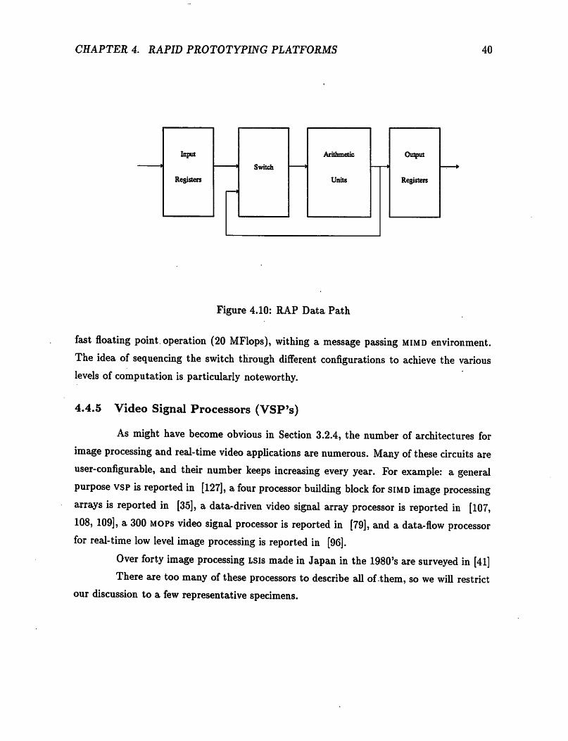
CHAPTER 4. RAPID PROTOTYPING PLATFORMS 40
Figure 4.10: RAP Data Path
fast floating point operation (20 MFlops), withing a message passing MIMD environment.
The idea of sequencing the switch through different configurations to achieve the various
levels of computation is particularly noteworthy.
4.4.5 Video Signal Processors (VSP's)
As might have become obvious in Section 3.2.4, the number of architectures for
image processing and real-time video applications are numerous. Many of these circuits are
user-configurable, and their number keeps increasing every year. For example: a generalpurpose VSP is reported in [127], a four processor building block for SIMD image processingarrays is reported in [35], a data-driven video signal array processor is reported in [107,108, 109], a 300 mops video signal processor is reported in [79], and a data-flow processorfor real-time low level image processing is reported in [96].
Over forty image processing LSis made in Japan in the 1980's are surveyed in [41]There are too many of these processors to describe all of them, so we will restrict
our discussion to a few representative specimens.

CHAPTER 4. RAPID PROTOTYPING PLATFORMS
Qocna
Inpa
Onral
Rccfcun
batu
JT To
Nownk
Cbaml
Rcctsm
Figure 4.11: RAP Block Diagram
Philips VSP
tops
Qots*
41
The Philips VSP chip targets real-time video signal processing [127]. Each chip
contains three Arithmetic Logic Elements ales, and two Memory Elements MEs, connected
by a full crossbar switch (Fig. 4.12). Connections to the crossbar switch are made through
so-called silos, which is a 32 word, two port ram which are used to provide algorithmic
sample delays. The ales are deeply pipelined (five stages). The MEs contain 512 words
each. Each PE is controlled by its own control memory P, which accommodates up to 16
instructions. In this architecture, the program is cyclically repeated, without any breaks,
by avoiding conditional branches.
The ALE blocks are shown in Fig. 4.13. Arithmetic and logic operations are possi
ble. It has two data inputs for ALU operations. A third input is used for partial multiplica
tions and to enable data dependent operations by supplying a parameter for the instructions
stored in P. In this way data-dependent instructions are realized without using conditional
branches.
The techniques such as employing a fully crossbar switch and the philosophy of
polycyclically executing a repetitive kernel make this architecture very interesting. The
target application domain is closely related to to that of this work. However, we observe
that the granularity and level of pipelining of the processors (ales), the fixed word widths

CHAPTER 4. RAPID PROTOTYPING PLATFORMS
CROSSBAR
SWITCH
f lilt 11 lilt 1111
LI uME ME
. moutputs .
42
Figure 4.12: Philips VSP
of 12 b, and the choice to allocate large resources to on board memory support, limit its
applicability for rapid prototyping of high speed data paths. A fixed word width narrows
its applicability to certain video applications. Its deep ALE pipelines are not well suited to
efficient calculation of recursive loops and conditional branch type instructions.
ITT DataWave
The ITT DataWave is a so called "Wavefront Array Processor for Video Applica
tions" [107,108,109]. The processor topology is an array of16 individually programmablemesh-connected cells (Fig. 4.14). The processor executes statically scheduled data flowprograms, propagating data through the array in a wavefront-like manner.
In this data-driven approach, cells automatically wait when neighbors are notready to send or receive data. Built-in hardware supports an asynchronous self-timed
4-phase handshake protocol. A major benefit of adopting an asynchronous paradigm isimmunity to clock skew, which is critical at very high clocking frequencies. Eight deep fifobuffers smooth out the data transmissions between cells.
The cells have 12b word widths and communicate with nearest neighbors throughinput and output FIFOs. The core cell with its execution units and program ram is surrounded by three 12b ring buses (Fig. 4.15). This bus enables a result from the core cell to

CHAPTER 4. RAPID PROTOTYPING PLATFORMS
FromP
Figure 4.13: PhiUps VSP: ALE Block Diagram
12 * v Nonh >.12
Bos Switch
12 12
Wen East
• f
12 12
Bm Switch
12 ^ * jioud1.12
Figure 4.14: DataWave: Processor Architecture
43
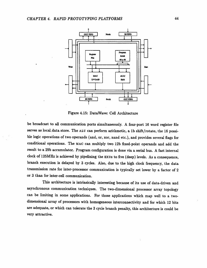
CHAPTER 4. RAPID PROTOTYPING PLATFORMS
Wot
our FIFOT ♦ *
Register
Pile
MAC
12*124-29
North
IIN FIFO Sotuh
T
IN FIFO
Pfognxn
RAM
64x48
ALU/
Shift
ehOUT FIFO
44
East
Figure 4.15: DataWave: Cell Architecture
be broadcast to all communication ports simultaneously. A four-port 16 word register file
serves as local.data store. The ALU can perform arithmetic, a lb shift/rotate, the 16 possi
ble logic operations of two operands (and, or, xor, nand etc.), and provides several flags for
conditional operations. The MAC can multiply two 12b fixed-point operands and add the
result to a 29b accumulator. Program configuration is done via a serial bus. A fast internal
clock of 125MHz is achieved by pipelining the EXUs to five (deep) levels. As a consequence,branch execution is delayed by 3 cycles. Also, due to the high clock frequency, the data
transmission rate for inter-processor communication is typically set lower by a factor of 2
or 3 than for inter-cell communication.
This architecture is intrinsically interesting because of its use of data-driven and
asynchronous communication techniques. The two-dimensional processor array topologycan be limiting in some applications. For those applications which map well to a two-
dimensional array of processors with homogeneous interconnectivity and for which 12 bits
are adequate, or which can tolerate the 3 cycle branch penalty, this architecture is could bevery attractive.

CHAPTER 4. RAPID PROTOTYPING PLATFORMS 45
Figure 4.16: NTT VSP Architecture
4.4.6 NTT VSP
The NTT VSP [79, 80] contains four pipelined data processing units (dpus) and
three parallel i/o ports (Fig. 4.16). Communication among the dpus and four sets of
cache memories occurs via eight 16b buses. The DPUs are pipelined to five levels. The
DPUs are controlled by local program units (16w x 32b) which are in turn sequenced by a
central program sequencer containing 512w x 32b of instructions. These units are initially
configured via a boot-rom which employs appropriate "set-up" commands. This vsp has
the advantage of having a very high data memory bandwidth and is attractive for specific
video processing such as video codecs.
4.4.7 Software Reconfigurable Transceiver
A programmable DSP engine for high-rate modems is was presented in [6]. The
architecture contains a fir processor for signal processing applications and a binary proces
sor for data manipulation. The fir processor contains three fir engines in a multiprocessor
simd architecture with a 32b instruction set dedicated for dsp tasks. The binary processor
contains a general purpose unit for cascading, error computation, error scaling, slicing, A/D

CHAPTER 4. RAPID PROTOTYPING PLATFORMS 46
and D/A interface, TDM interface, AGC etc.
The device is fully programmable as a transmitter, echo canceller, equalizer, deci
sion feedback equalizer. It supports programmable filter structures, programmable adapta
tion modes, programmable adaptation rates, programmable filter rates, has software recon
figurable interconnections, zero-glue interface to most processors and programmable support
functions.
While the data rates (5 Mb/sec) are not as high as the applications that we
consider, this processor is an good example of the effective use of software-configurable
techniques to its application domain to provide flexibility and high performance.
4.4.8 Field Programmable Gate Arrays
Programmable or restructurable devices known as programmable logic devices
(PLD's) (such as [5]) are able to implement random logic and simple fsms rather well.
Prior to these devices, any glue logic or simple controllers would typically require several
or many TTL parts depending on the complexity. With these devices, the chip count canbe dramatically reduced.
In recent years, the class of chips known as fpgas has seen rapid growth [40].Examples are numerous and new ones are continually being reported. Among the manypopular ones are: Xilinx [52, 51, 130], Actel [4], Algotronix (Cal) [45], Plessey [46], att[48], and Plus Logic [94]. These devices are of similar architecture and granularity in thatthey all consist of some form of configurable logic block clb connected by some form ofprogrammable interconnect.
It would be impractical and unnecessary to discuss all members of this class. We
will choose the popular xilinx XC3000 fpga as a representative. Fig. 4.17 shows the basiclogic cell array layout. Alogic cell array consists ofaset of clbs which are user-configurable.Other user-configurable structures are the programmable interconnect and the i/o blocks,or iobs.
The basic clb architecture is outlined in Fig. 4.18. It contains two sections, onecombinational logic, the other, registers. The combinational logic section is implementedas a thirty-two entry lb sram. With this structure, several choices of combinational logicfunctions are possible as shown in Fig. 4.19. The basic interconnection structure is shownin Fig. 4.20.

CHAPTER 4. RAPID PROTOTYPING PLATFORMS
PART CLB's I/O
3090 320 144
3064 224 120
3042 144 96
3000 100 80
2000 64 64
programmable interconnect
perimeter of IOBs
array of CLBs
Figure 4.17: XC3000 Logic Cell Array Family
COMBINATIONAL
LOGIC
R
Din
STORAGE ELEMENTS
-zh_rhljF— J D Q—i—H>CE I
— XA —
B —
C —
D —
E —
R
D Q
~t>CE tO-CLOCK
\yCB
Figure 4.18: XC3000 CLB Architecture
47

CHAPTER 4. RAPID PROTOTYPING PLATFORMS
CH
tH
my fimcdoaof up to 4vtritMcf
tsy faacdogof up to 4
vuublet
my function
of5 viritbles
Figure 4.19: XC3000 Combinational Logic Options
!CLB CLB
1
Switch
Minx
IIi i
iii !
CLB CLB
O DtnctCaoieci to4Nuictt neighborCLB'fO GeDBilPupoMbferconscciiSwftkiLShoriuBa]O I.mgl.tnM-4V«Tti.T»l,3W»i»»..|
Figure 4.20: XC3000 Interconnect Structure
48

CHAPTER 4. RAPID PROTOTYPING PLATFORMS 49
These devices are changing the way many system designs are being implementedand prototyped. Because they are software-configurable, and have robust simulation tools,designs which might take weeks to fabricate in an asic can now be done in a matter of
hours. As the level of integration increases, the number of usable gates will continue to
grow into the tens of thousands. Since many actual designs typically contain gates of this
order ofmagnitude, fpgas .have and will continue to becompetitive with conventional gate-arrays for low to medium complexity designs. Active research is also currently being done
in the field of logic synthesis for fpgas [81, 82, 39] and in incorporating them as hardware
platforms into high level synthesis systems [132].
Due to their bit-level granularity, fpgas will not support as flexible routing of
wide data-buses and will not have as fast adders (for the same technology) as a word-level
granular architecture with flexible bus interconnections and adders optimized for speed.
FPGAs also do not typically support hardware multiplexing of their clbs which can lead to
highly inefficient designs in some cases. For these reasons, fpgas will have limitations in
the prototyping of high speed data paths. These limitations will be further elaborated on
in Appendix A.
4.4.9 PADDI: Programmable Arithmetic Devices for High Speed DSP
In Chapter 2, we discussed the computational requirements for real-time DSP ap
plications, in Chapter 3, we discussed taxonomies which would help us differentiate between
the many architectural styles found in digital signal processing. There we focussed on the
arithmetic/control ratio as an appropriate metric and discussed the merits of hard-wired
data path approaches for high speed digital signal processing. In the previous sections of
this chapter, we have argued the need for rapid system prototyping, and the advantages
of software-configurable hardware approaches. We have discussed specific case studies of
systems and ics which use configurable hardware approaches. While these approaches serve
their particular application domains very well, none of them are well suited to rapid pro
totyping of real time digital signal processing applications, specifically those which require
hard-wired data path solutions because of their high speed computations, and low arith
metic/control ratio.
Clearly what emerges is the need for some type of programmable engine which
lends itself to the rapid prototyping of high speed data paths. From Section 2.5 we re-

CHAPTER 4. RAPID PROTOTYPING PLATFORMS 50
iterate the basic architectural features which must be supported by such an engine:
a) a set of concurrently operating execution units (exvs) with fast arithmetic, to
satisfy the high computation (hundreds ofuovs) requirements.
b) very flexible communication between the EXUs to support the mapping of a
wide range of algorithms and to ensure conflict free data routing for efficient hardware
utilization.
c) support for moderate (1-10) hardware multiplexing on the EXUs, for fast computation of tight inner loops.
d) support for low overhead branching between loop iterations.
e) wide instruction bandwidth.
f) wide i/o bandwidth (hundreds ofMB/sec).
The basic concepts for such an engine, PADDI, or Programmable Arithmetic De
vices for High Speed Digital Signal processing, were first reported in [25]. The abstract
architecture, shown in Fig. 4.21, is similar, but not identical to those of the software-
configurable architectures presented in the previous sections. The set of exus are repre
sented as data processors. The nx n switch provides flexible communication. Performance
is achieved through increased parallelism rather than increasing the level of pipelining ofthe EXUs, which better satisfies c) and d). In order to satisfy both e) and f) simultaneously,a two level instruction decoding scheme is employed. The local IPs which directly control
the dps are serially configured at configuration time. At run-time, they receive instructions
from an external IP via a 1-n switch. What sets this architecture apart from the othersmentioned previously is the granularity the EXUs, the instruction set, and the allocation of
resources to specifically support high speed data paths. The architecture will be presentedin detail in Chapter 5.
4.5 Conclusions
In this chapter we discussed the need for rapid prototyping in general, and fordsp applications in particular. We also discussed various methods which can be em
ployed to achieve a rapid prototyping capability. A promising approach is that of software-configurable hardware. We have discussed several architectures which employ this approach.While many such architectures exist for a variety of applications, none are well suited for
rapid prototyping of the high speed data paths found in real time dsp. We also presented

CHAPTER 4. RAPID PROTOTYPING PLATFORMS
NxN
Instruction
Memory
Hierarchy
Figure 4.21: PADDI Abstract Architecture
an abstract view of the paddi architecture which was created to fill this gap.
51

Chapter 5
PADDI: Architectural Design
Fallacy: One can design a flawless architecture
— J. Hennessy and D. Patterson, Computer Architecture A Quantitative Approach
5.1 Introduction
The goal of this chapter is to describe the development and design of an archi
tecture which targets the rapid prototyping of high speed data paths for real-time digital
signal processing applications.
In Chapter 2 we discussed the computationand i/o requirements of real-time dsp
applications. Many high speed dsp systems employ a hard-wired pipelined data path ap
proach to attain the requisite high computation rateThe merits of the hard-wired pipelined
data path approach were discussed in Chapter 3. Chapter 4 focussed on rapid prototyping
platforms for high speed dsp systems. There we identified software-configurable hardware
to be a very promising approach to attaining the dual goals of flexibility for rapid proto
typing and high computation rate. We discussed several examples of software-configurable
hardware architectures and identified the need for one that addresses real-time dsp. In this
chapter wedescribe the development and design of such an architecture, namely, the paddi
architecture. The acronym paddi stands for "Programmable Arithmetic Devices for HighSpeed Digital Signal Processing".
We shall begin with a discussion of how paddi was developed. As we present
the architecture, we will explain the reasons for some of the key design choices and we
will discuss the various techniques used to achieve high performance. The programmer's
52
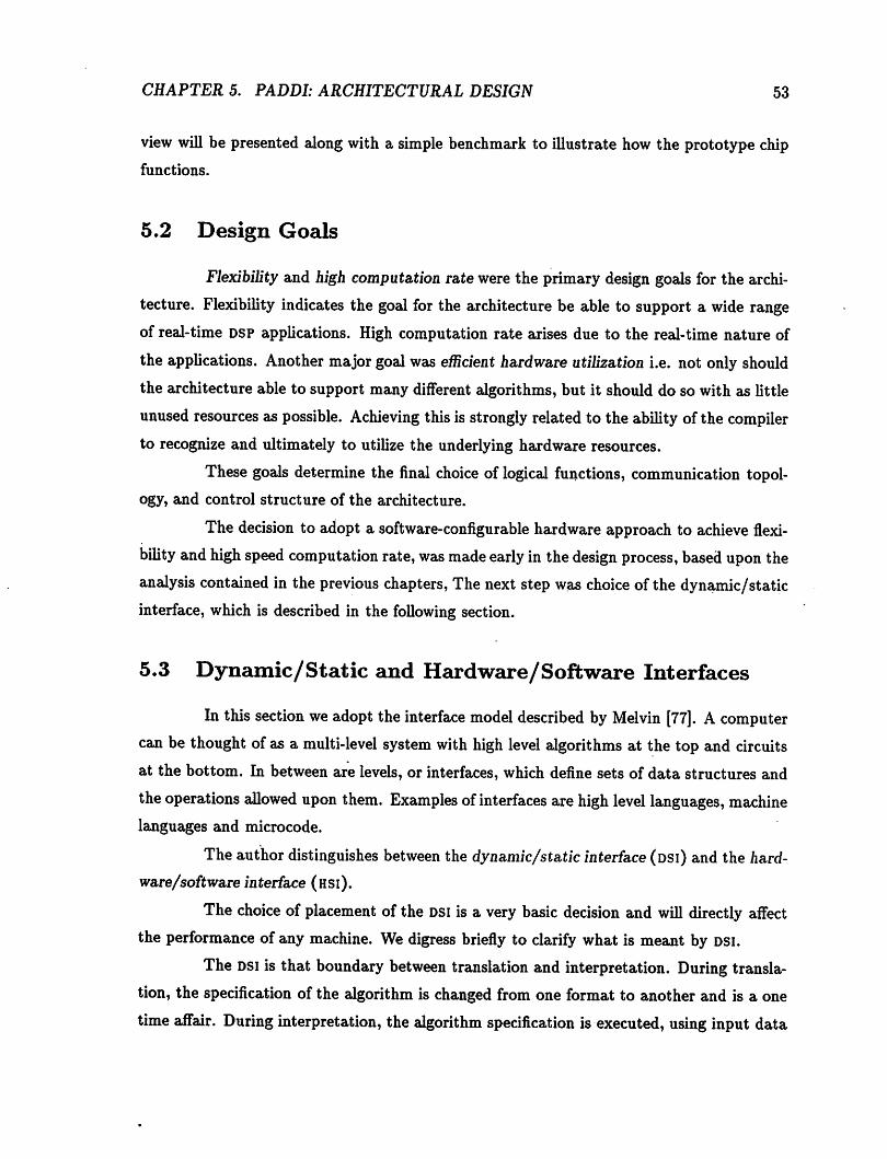
CHAPTERS. PADDI: ARCHITECTURAL DESIGN 53
view will be presented along with a simple benchmark to illustrate how the prototype chip
functions.
5.2 Design Goals
Flexibility and high computation rate were the primary design goals for the archi
tecture. Flexibility indicates the goal for the architecture be able to support a wide range
of real-time dsp applications. High computation rate arises due to the real-time nature of
the applications. Another major goal was efficient hardware utilization i.e. not only should
the architecture able to support many different algorithms, but it should do so with as little
unused resources as possible. Achieving this is strongly related to the ability of the compiler
to recognize and ultimately to utilize the underlying hardware resources.
These goals determine the final choice of logical functions, communication topol
ogy, and control structure of the architecture.
The decision to adopt a software-configurable hardware approach to achieve flexi
bilityandhigh speed computation rate, was made early in the design process, based uponthe
analysis contained in the previous chapters, The next step was choice of the dynamic/static
interface, which is described in the following section.
5.3 Dynamic/Static and Hardware/Software Interfaces
In this section we adopt the interface model described by Melvin [77]. A computer
can be thought of as a multi-level system with high level algorithms at the top and circuits
at the bottom. In between are levels, or interfaces, which define sets of data structures and
the operations allowed upon them. Examples of interfaces are high level languages, machinelanguages and microcode.
The author distinguishes between the dynamic/static interface (dsi) and the hardware/softwareinterface (hsi).
The choice of placement of the DSI is a very basic decision and will directly affect
the performance of any machine. We digress briefly to clarify what is meant by dsi.
The dsi is that boundary between translation and interpretation. During transla
tion, the specification of the algorithm is changed from one format to another and is a one
time affair. During interpretation, the algorithm specification is executed, using input data
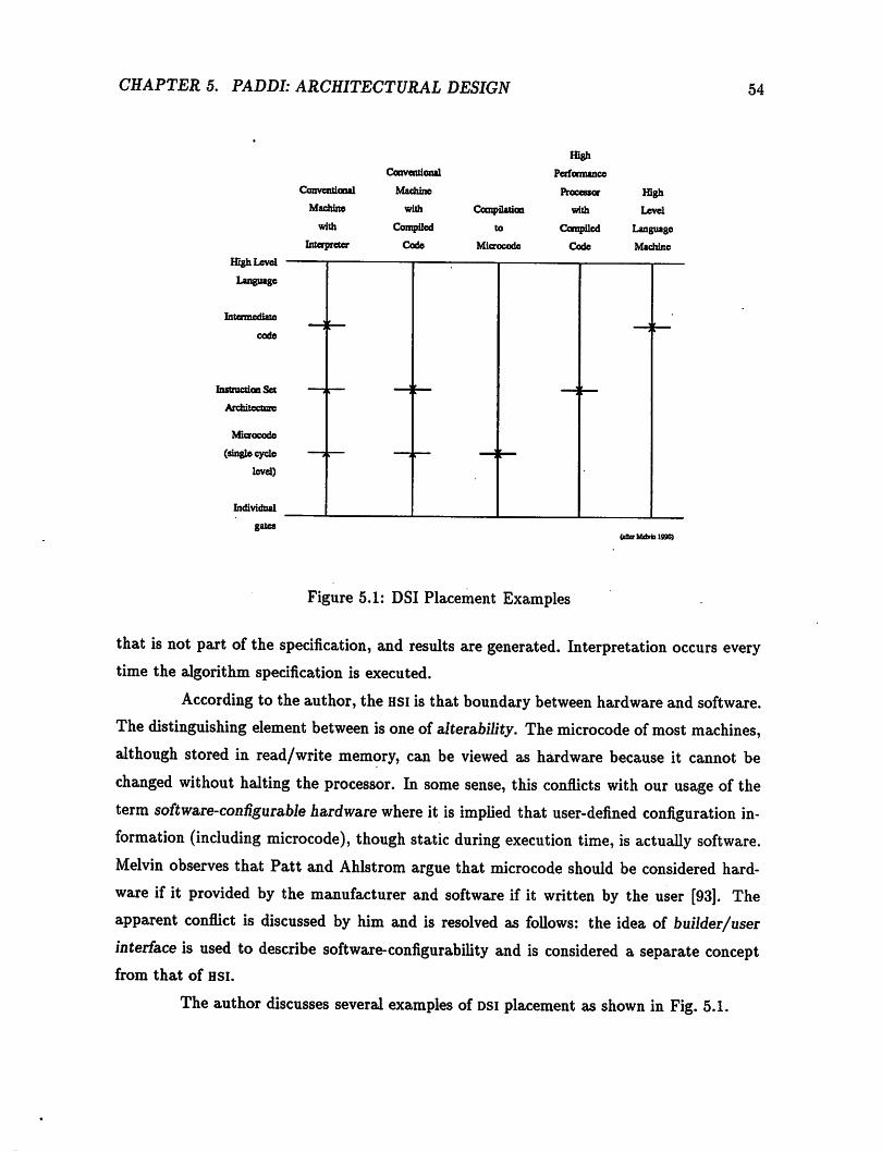
CHAPTER 5. PADDI: ARCHITECTURAL DESIGN
High
Conventional Performance
Conventional Machine Processor High
Machine with Compilation with Level
with Compiled to Compiled Language
ti:Du t «im»i -
Interpreter Code Microcode Code Machine
XUgfl U6VG1
Language
Litennediate
^
i
code
Instruction Set
Architecture
t I J!
i k ~^ l
Microcode
(single cycle 7 > i 5
level)
Individual
gatesUttaMdvfalSUO)
Figure 5.1: DSI Placement Examples
54
that is not part of the specification, and results are generated. Interpretation occurs every
time the algorithm specification is executed.
According to the author, the HSI is that boundary between hardware and software.
The distinguishing element between is oneof aiterability. The microcode of most machines,
although stored in read/write memory, can be viewed as hardware because it cannot be
changed without halting the processor. In some sense, this conflicts with our usage of the
term software-configurable hardware where it is implied that user-defined configuration in
formation (including microcode), though static during execution time, is actually software.
Melvin observes that Patt and Ahlstrom argue that microcode should be considered hard
ware if it provided by the manufacturer and software if it written by the user [93]. The
apparent conflict is discussed by him and is resolved as follows: the idea of builder/user
interface is used to describe software-configurability and is considered a separate conceptfrom that of hsi.
The author discusses several examples of dsi placement as shown in Fig. 5.1.

CHAPTER 5. PADDI: ARCHITECTURAL DESIGN 55
The first example represents a conventional interpreter. The high level language
program gets translated into an intermediate level code. It then gets interpreted by a
program running on a conventional microprogrammed machine. There are three levels of
interpretation involved: the intermediate level code by the machine level code, the machine
level code by the microcode, and the microcode by the gates. The second example rep
resents a conventional microcoded machine running compiled code. Here the intermediate
code step is eliminated. The third example represents reduced instruction set machines
which puts the dsi (and hsi) at the lowest level possible. The fourth example represents
a higher performance version of the second example. Here, the microcode interpreter has
been eliminated and the machine language level is executed directly. If the instruction set
architecture is designed specifically with a hard-wired implementation in mind, the distinc
tion between the third and the fourth examples blurs. The final example represents a highlevel language architecture. The author quotes examples of actual machines for each case.
At the beginning ofour architectural design, the choice was made to place the DSI
ofour processor as in example three discussed above. As was observed in Chapter 2, realtime dsp algorithms are typically implemented on pipelined data paths, which are either
fully pipelined (the hardware multiplexing ratio is one), or execute tight inner loops (thehardware multiplexing ratio can range from one to ten). The choice of adopting a Risephilosophy dove-tailed with this for the following reasons. Firstly, a reduced instruction
set evolves naturally from the digital signal processing domain. The instructions that are
required are naturally restricted to arithmetic and comparison types due to inherent nature
of the computations. Secondly, since these instructions execute repeatedly in pipelinesand/or in loops, the performance gain of a simplified, but faster design, will be magnifiedmany-fold as they are continually repeated over time.
Having committed to this choice of DSI, the next step was to evaluate the fre
quency of individual functions and optimize the performance of those that were used most
frequently. Essentially, the problem was one of chosing the HSI.
5.3.1 Design Methodology
Adesign methodology ofsuccessive refinement was used to develop the architecture
(Fig. 5.2). The successive refinement consisted of two phases, one ofanalysis, and one ofsynthesis.

CHAPTER 5. PADDI: ARCHITECTURAL DESIGN
Examine benchmarks
Define architecture,
primitive operators,
interconnect, control
10
Evaluate primitives,
interconnect, control & 10.
Reject complicated ones
Evaluate new benchmark
or recast old one
Compare performance
to existing architectures
analysis
synthesis
analysis
Figure 5.2: Architectural Design Methodology
56

CHAPTER 5. PADDI: ARCHITECTURAL DESIGN 57
In the analysis phase, a benchmark was evaluated for its particular architectural
requirements, namely its primitive operators, its interconnect, its control, and its i/o re
quirements. Basedon the results of the analysis, we could, in the synthesis phase, construct
or modify an architecture to support this benchmark. If a certain feature was not used
very often, or would complicate the architecture, it was rejected. Additionally, the final
architecture was compared to existing designs such as discussed in Chapter 4. The final
justification of the design lay in its ability to out-perform prior ones. Our objective was to
create as simple an architecture that would meet the design goals. By keeping things sim
ple, we wanted to maximize our chances for achieving functionality, high speed and efficientcompilation.
5.3.2 Functional Design
Listed below are some of the main algorithms that were used as benchmarks.
Biquadratic filters were a simple and convenient benchmark with which to get started.
The architecture can support non-recursive filters but recursive biquadratic filters are more
interesting because their feedback structure puts more of a burden on the architecture.
Filtering
• a) biquad
- hardware multiplexed
- direct-mapped
- pipelined [112, 92]
Video and Low Level Image Processing
b) Video Matrix Converter [88]
c) 3x3 Linear Convolver [104]
d) 3x3 Nonlinear Sorting Filter [104]
e) Memory Controller For Video Coding [106]Speech Recognition
• f) Dynamic Time Warp [58]
• g) Word Processor [116, 115]
• h) Grammar Processor [22]
The basic features that must be supported by the architecture were listed in Sec
tion 4.4.9. These were:

CHAPTER 5. PADDI: ARCHITECTURAL DESIGN
DATAPATH ARITHMETIC OPERATORS CONTROL DATA
I/O
pipelined, 8-18b unsigned + - shiftlocal branch
8-1121/P
parallel 8-24b2'sc 1/2.. 1/128 global branch 8 - 51 O/P
heterogenous saturation compare
communication min, max
ace, mult
Figure 5.3: General Characteristics of Benchmark Set
58
a) a set of concurrently operating execution units (exvs) with fast arithmetic, tosatisfy the high computational (hundreds of mops) requirements.
b) very flexible communication between the EXUs to support the mapping of awide range of algorithms and to ensure conflict free data routing for efficient hardwareutilization.
c) support for moderate (1-10) hardware multiplexing on the exvs, for fast computation of tight inner loops.
d) support for low overhead branching between loop iterations.
e) wide instruction bandwidth.
f) wide i/o bandwidth (hundreds ofMB/sec).
Figure 5.3 is a summary of the general characteristics of the benchmark set and
show specific features that need to be supported. The common theme to the data paths
examined was the requirement for many operators to be executing in pipelined and parallel
fashion, with a widely varying or heterogeneous communication between them. Typically
the arithmetic was unsigned or two's complement, ranged in required accuracy from 8b to
24b, and was saturating. Operations were mainly limited to addition, subtraction, shifting,
comparison, accumulation max and min, and multiplication. Two forms of low overhead
branching were required. Local branches where the result of one operator was used to

CHAPTER 5. PADDI: ARCHITECTURAL DESIGN
NUMBER of OPERATIONS
30
20
10
abcdefgh
add/sub shift comp 2:1 max
OPERATION
4:1 mux
59
abs malt
Figure 5.4: Number of Ops vs. Op Type
control the output of another, and global ones where the result of an operator influenced
the global instruction sequence. The i/o pin count for the various implementations that
were examined exhibited a wide range as shown, which gives some insight into the i/o
resource requirements. The combination of Table 2.1 which summarizes the computations
and i/o bandwidth requirements and Figure 5.3 which lists specific characteristics were
used to guide the design of the architecture. The detailed results of this study are describedbelow.
Operator Statistics
A count of the different operations present in each algorithm (a - g) listed above
was compiled. The result, for each algorithm, is shown in Figure 5.4. The assumptions
made for the fixed coefficient biquadratic filter (case a) was that on average, four shifts
were required after canonic-signed digit conversion. Max and min functions functions were
decomposed into compare and multiplexing operations. The abs and mult (variable by vari
able) operations were only present in the dynamic time warp example. As to be expected,
the add/sub operation is dominant for all algorithms.
Further perspective can be gained by summing a particular operation e.g. all
additions, across all the algorithms. The result is presented in Figure 5.5. The percentage

CHAPTER 5. PADDI: ARCHITECTURAL DESIGN 60
occurrence of all occurrences is also listed. Clearly, by adopting the ten percent rule,
architectural support for add/sub, shifts, comparisons, two to one multiplexing is desirable.
Interconnect Statistics
A count was made of the connectivity of the different operations in each algorithm
i.e. (a - g), listed above. The result for each algorithm is shown in Figure 5.6. Here l:m
denotes an arc in the signal flow graph which connects a single source to m destinations,
and n:l denotes an arc which connects n sources with one destination. As to be expected,
the 1:1 arcs are dominant for all algorithms sue to the spatial locality of the computations.
Further perspective can be gained by summing arcs across all the algorithms. The
result is presented in Figure 5.7. The percentage occurrence of all occurrences is also listed.
We observe that 1:1 connections dominate by occurring 78.9% of the time, 1:2 connections
15.0 %, 1:3 connections. 2.4 %, 1:4 connections 1.7 %, 1:5 connections 0.7 %, 1:5 connections
0.2 %, 2:1 connections 0.5 %, and 4:1 connections 0.2 %.
Becauseof the close correspondence between the operators-and hardware execution
units in fully pipelined applications, We can reasonably associate operator connectivity with
execution unit connectivity. We can deduce from the high percentage of 1:1 and 1:2 arcs
that there is tremendous spatial locality in the usage of variables. This spatial locality
arises as a direct consequence of pipelining where operational units tend to communicate
with neighbors. In these considerations, the statistics will change depending upon the level
of hardware multiplexing which is allowed. Clearly when several operations are executed
upon the same hardware unit, the distribution of the various types of arcs will change. For
example, the need for data merging into a single destination (over several cycles) will beclearly be greater.
Control Statistics
Thetypes ofcontrol structures required for each algorithm islisted in Figure 5.8. Inmany of the algorithms, the applications are fully pipelined and so the the control structure
is degenerate i.e. none is required. Others typically require the repetitive execution of asmall loop.
An example of such a loop is outlined in Figure 5.9. It is the control loop for the
grammar processorof the grammar processing subsystemofexampleh. The state transition

CHAPTER 5. PADDI: ARCHITECTURAL DESIGN
90
80
70
60
50
40
30
20
10
Total Number of Operations
37.6%
. _..{>C..Q4R.. .._ „..ZD.OT©
% --15.8% 16:39
0.9% 1.8% 1.8%
< X M H M X X •
add/ sh comp 2:1 4:1 abs mult
sub mux mux
OPERATION
Figure 5.5: Total Number of Ops vs. Op Type
61

CHAPTER 5. PADDI: ARCHITECTURAL DESIGN
60
SO
40
30
20
10
NUMBER
r-|
r-
"
™
-i
abed
<
efgh f*
• ffL_nr}Jl _ ^X H M X— •
1:1 1:2 1:3 1:4 1:5 1:6
FANOUT
Figure 5.6: Number of Arcs vs. Arc Type
62
diagram for the grammar processor consists of eight states. The first two perform processor
initialization. In the third state, the processor idles until a word is available at the input
FIFO. Upon receipt of this word, it performs several state transitions to fill the processor
pipeline until the last state is reached. At this point, the pipeline is full and the processor
executes within state until all successors of the word are updated, or the current probability
falls below a dynamically adjusted threshold, whichever comes first. The processor then
returns to the third state to await the next word. The above example illustrates the the
ability of the processor to perform conditional branches, and to perform several different
instructions in a tight loop.
From these examples we discern that the processor we design should be capable
of efficiently performing global branches, as well as the degenerate case of full pipelining
of the EXus. What might not have been clear is the need for efficient performance of
local branches. In many of the benchmarks, the result of one operation directly affects
the outcome of another. Examples of this are evident in the data path of the Grammar
Processor which waspresented in Fig. 2.4. In this way, high performance is achieved because
the conditional operation is directly hard-wired into the data path. Our processor should
also be capable of handling these cases efficiently.

CHAPTER 5. PADDI: ARCHITECTURAL DESIGN
TOTAL NUMBER
350
78.9%
300 -
250 -
200
150
100
50
(2:1 0.5%, 4:1 0.2%)
15.0%
2.4%1.7%
0.7% 0.2%
< M M X M M •1:1 1:2 1:3 1:4 1:5 1:6
FANOUT
Figure 5.7: Total Number of Arcs vs. Arc Type
63

CHAPTER 5. PADDI: ARCHITECTURAL DESIGN
BENCHMARK CONTROL
a) biquad
(pipelined)
fully pipelined
a) biquad (hardware
multiplexed)
control loop
b) video matrix
convener
fully pipelined
c) 3x3 Linear
Convolver
fully pipelined
d) 3x3 Non-linear
Sorting Filter
fully pipelined
e) Memory Controller fully pipelined
f)DTW control loop
g)WordProc control loop
h) Grammar Proc control loop
Figure 5.8: Control Structure by Benchmark
64

CHAPTER 5. PADDI: ARCHITECTURAL DESIGN
FILL
PIPELINE
READ OFFSET
READ RMIN, SET WCIR
PROB < THRESH
or ENDLIST
READ SUCC ADDRESS tBd TRANSITION PROB
UPDATE SUCC ADDRESS COUNTER
READ OLD PROB FROM PRIOR UPDATE
WRITE NEW PROB FOR CURRENT UPDATE
Figure 5.9: Grammar Processor Control
BENCHMARK CLOCK
(MHz)
INPUT OUTPUT
PINS BW
MBIsec
PINS BW
MBIsec
a) biquad
(pipelined)4 16 8 16 8
a) biquad (hardware
multiplexed)24 16 48 16 48
b) video matrix
converter27 24 51 48 162
c) 3x3 Linear
Convolver10 24 30 8 10
d) 3x3 Non-linear
Sorting Filter10 24 30 8 10
e) Memory Controller 8 12 12 36 36
f)DTW 5 32 20 16 10
g) Word Proc
(Viterbi only)
5 54 34 42 26
h) Grammar Proc
(excl. Epsilon Proc)
5 68 43 64 40
Figure 5.10: 10 Statistics
65

CHAPTERS. PADDI: ARCHITECTURAL DESIGN 66
IO Statistics
The i/o statistics are shown in Figure 5.10.
In this figure wesee the inclusion of two versions of the biquadratic filter. The first
assumes that the filter runs at 4 MHz. The second assumes that transformations are made
(using techniques described in [112, 92]) to pipeline the filter to achieve a sampling rateof24 MHz. Both assume that the filters are 16 bits. For the linear convolver and the non-linear
sortingfilter (examples c and d), we assume that the line delays exist external to the system.
This assumption is made to reflect the fact that our targeted architecture does not support
the implementation of video line delays. This allows a more accurate accounting of the
i/o requirements of these benchmarks. Actual pin numbers were available for the Viterbi
Processor section of the Word Processing Sub-system of benchmark g, and the Grammar
Processor of the Grammar Processing Sub-system of benchmark h which is why we have
tabulated these cases.
The main conclusion that can be drawn from these numbers is that real-time
algorithms place a heavy burdenon the pin and i/o bandwidth requirements of the systems
that implement them.
Computation Rate Statistics
The computation rate statistics for the different benchmarks are presented in Fig
ure 5.11. The computationrate is calculated as the product of the total numberofoperations
(excluding data moves) and the clock rate.
Here al and a2 refer to the two versions of the biquadratic filter. The Viterbi
Processor of the Word Processing Sub-system is labeled as gl, and the total requirements
of the whole word processing sub-system is labeled as g2. As mentioned in Chapter 2, this
system has been upgraded to handle 60,000 words in real-time with 30 accesses per state
which require in excess of 600 MB/sec of i/o bandwidth [115]. This upgraded system is
labeled as g3. The grammar processor section of the Grammar Processing Sub-system is
labeled as hi, and the total requirements of the grammar processing sub-system is labeledash2.
In order to estimate the balance of the required computation rate and the i/o
bandwidth of these systems, we can tabulate the ratio of these two metrics, as shown in
Figure 5.12. These results are plotted in Figure 5.13. The arithmetic mean of the ratio is 6.4

CHAPTER 5. PADDI: ARCHITECTURAL DESIGN 67
Computation Rate (MOPs)
3000
2000
1000
« H M M M M H M H M M M •al a2 b c d c f gl g2 g3 hi h2
BENCHMARK
Figure 5.11: Computation Rate Statistics
Mops/MB/sec. A betterestimate (to reduce the effect ofoutliers) is probably the geometric
mean which is 3.56 Mops/MB/sec. Clearly, if our final architecture digresses greatly from
these values, it should serve as a warning flag of possible imbalance of resources.
5.4 Techniques for High Performance
A popular measure of the performance of conventional uni-processors is the time
required to accomplish a specific task (or program, or algorithm, or benchmark). It is often
expressed as the product of three factors:
Time per Task = C * T * I
C = Cycles per instruction
T = Time per Cycle (clock speed)
I = Instructions per Task
Fig. 5.14 shows the task set for a uni-processor and a corresponding task set for
the prototype chip. If, for argument's sake, we assume this naive mapping, then several
points are clear. For each individual EXU, the above performance metric still applies. The
mapping is of course naive, since, by applying such techniques as pipelining and parallelizing
operations across EXUs, operator chaining within EXUs, pipelining within EXUs, one can

CHAPTER 5. PADDI: ARCHITECTURAL DESIGN
30
20
10
BENCHMARKCLOCK
(MHt)
COMP
(MOP*)
IOBW
(MM)
COMP/IO
(MOPl/MB/i)
t)Uqpal4 228 16 14.25
24 2640 96 27.5
bjndCOIStidJI
GOBVCSCT27 1674 21J 75
c)3*3Lfacv
Cmvolvcr10 170 40 405
<03i3Noo-tiaetf
SodtaaFOtcr10 280 40 7.0
o) Meotny OoomDcr 104 48 22
QDTW 176 30 5.9
Si) Word Proc
(VltaMcoly)130 60 22
(2) Ward Proc
(uul)22S 85 2A
|3)Ward Proc
(amded)320 600 09
al|USBUBff PlOB
(rrrl PprgoaPtoc)75 83 09
al/OMIIIIlfTPrUC
(told)200 265 0.75
Figure 5.12: Computation Rate / IO
ComputationRate(Mops)/ IO BW (MB/scc)
ArithMema6/t
GeomMeana3S6
1 1
< >< >< H M >< M M M X M X •al a2 b c d e fglg2g3hlh2
BENCHMARK
Figure 5.13: Computation Rate / IO
68

CHAPTER 5. PADDI: ARCHITECTURAL DESIGN
ins I
2
3
n
instructions
UNI-PROCESSOR
TASK SET
n/8
wide
instructions
EXUs
J!-
ins 1 2 8
9 10 16
n-7 n-6 n
PADDI
TASK SET
69
Figure 5.14: Naive Mapping of Uni-processor Task Set
dramatically reduce the number of wide instructions and, in the limit, approach I =1 for
a fully pipelined application. We will now discuss the various techniques which we have
applied to improving the performance. This work relies in part on the techniques used in
the popular Rise [57] approaches.
If we can reduce any of the individual components which contribute to the overall
time per task without increasing any of the other components in the process, we will have
improved the performance. Techniques which can be brought to bear on reducing C are
instruction pipelining, adopting a load/store architecture, using delayed branching and
filling the unused slots with useful instructions.
In order to reduce T one must attempt to optimize and equalize the various
critical paths of the machine. This is one of the strongest arguments for adopting a simple
rather than complicated architecture.
The primary techniques which help reduce I are resident in the compiler, will be
discussed in more depth in Chapter 7. For highest performance, the goal is to spread the
Task over as many EXU's as possible and, in the limit, approach 1 = 1. By minimizing
architectural constraints, eliminating special case situations and adopting an orthogonal
instruction set, the task of the compiler can be greatly facilitated. We therefore tried
to maintain a regular architecture with as few restrictions as possible and to expose the

CHAPTER 5. PADDI: ARCHITECTURAL DESIGN 70
underlying hardware to the compiler.
5.5 Processor Architecture
Having established our design goals, decided on a software-configurable hardware
approach, and settled on a DSI, the next step was to design the architecture based on the
analysis of the benchmark set presented above, and employing the various high performancetechniques presented.
At this point the problem was partitioned into its component pieces or modules,
namely functional blocks, interconnect, control, i/o, memory, and software con
figuration
We will now describe some of the basic design questions that arose for each of
the separate components. Design choices in a given component almost always influence the
design of the other components, and so it was not always possible to de-couple the-designs.
A major influence on the choice of design was the ability to have reasonably accurate
knowledge of the impact of a particular design choice upon the underlying silicon area and
the timing. Finally, the questions of Will the compiler be able to make use of this? and
Will this make it difficult to compile for? and How will this impact hardware utilization?
were constantly kept in mind.
5.5.1 Execution Units
We begin by re-iterating the relevant key architectural feature required for the
operational units that was identified in Section 2.5. The requirement was one of a set of
concurrently operating execution units with fast arithmetic, to satisfy the high computation(hundreds ofMOPs) requirements.
Design Considerations
Some of the major questions which needed to be answered for the functional block
design were Which operators should we support? Should the blocks resemble gate arraysor processors? What is appropriate granularity? and Should the blocks be homogeneous orheterogeneous in nature?
The question of which operators should be supported was answered by examining

CHAPTERS. PADDI: ARCHITECTURAL DESIGN 71
the general characteristics of the benchmark set as discussed previously. A decision was
made to adopt a processor or EXU based approach with moderate granularity. With this
approach, the desired functionality could be incorporated into the data path, optimized for
area and speed, and not consume any global routing resources that would be required in
a more granular approach. Additionally the overhead of configuring and controlling larger
blocks decreases linearly as the block size grows. The problem is that, as the block size
grows, the impact of an unused block becomes higher. This puts additional pressure on the
compiler to ensure that the hardware can be utilized as fully as possible. We considered
an initial block size of 8b with the possibility of linking the blocks together for 16b, 24b
and 64b accuracy. We finally decided upon a 16b architecture with linking capability for
32b operation in order to reduce the control overhead. A decision was made to adopt a
homogeneous architecture the regularity of which would be a plus for compilation efficiency.
Execution Unit Architecture
Fig. 5.15 shows the internal architecture of an EXU. It supports addition, subtrac
tion, saturation, comparison, maximum-minimum, and arithmetic right shift. Furthermore,
the EXUs can be user configured to be both 16b or 32b wide. Arithmetic is performed in
two's complement or unsigned format with automatic saturation.
Two register files each containing six registers are used for the temporary buffering
of data. The files are dual-ported for simultaneous read and writeoperations. They can also
be configured as delay lines to support pipelining and retiming of operations. In each file,
one of the six registers is configured as a scan-register. It can be initialized to contain an
arbitrary value (for the implementation of constant variables), read and written as a regular
register, or used for scan-testing. A fast carry-select adder and logarithmic shifter are used
to implement the arithmetic functions. A pipeline register is available at the output of each
EXU for optional use. By using the register, the user can increase the maximum sampling
rate by overlapping EXU operations with data transmission over the network. This can be
useful in applications where the additional latency has no negative effect. However, if the
operation is in a feedback loop, the additional pipeline register would normally not be used.
A status flag (a > b) is available to other EXUs and the external world.
The basic paddi operations are shown in Fig. 5.16 and Fig. 5.17 respectively.
There are no fundamental reasons, save area, that limit the EXU to the one used

CHAPTER 5. PADDI: ARCHITECTURAL DESIGN
r1 C v1 I,
-RBO--HtS- "HtS-
I\sunn ^^t-
"V—^
P-L-,1
ptpcuoo
g WORDS
NANOSTORE
Figure 5.15: EXU Architecture
n r
TADD/SUB
SATURATION
ACCUM
MAX(A,B)
MIN(A3)
SHIFT/(ADD/SUB)
COMPARE
Figure 5.16: Primitive PADDI Operations (a)
72

CHAPTER 5. PADDI: ARCHITECTURAL DESIGN
2
y OPTIONAL
PIPELINE REGISTER
PROGRAMMABLE
DELAY LINE
i 16 f 16
LINKABLE DATA-PATHS
k
1. U.
2 PORT
REG FILES
73
= s: /
A ^j
XT
PASSA/B
Figure 5.17: Primitive PADDI Operations (b)
in paddi or the number of nano-store instructions to eight. For a different application set,
one might indeed wish to modify the EXU design and increase the number of nano-store
instructions.
A decision was made to not implement a dedicated hardware multiplier due to
area cost. Many commercially available chips already exist which are essentially multiply-
accumulate engines. These engines are tuned for algorithms which require lots of multipli
cations. However, as our benchmark set indicates, for many applications, the presence of
a multiplier becomes a costly burden because it would be an under-utilized resource. The
architecture of the exus can be easily modified to support modified Booth coded, multi
cycle multiplication using shift and adds. Such a modification may be included in future
versions.
We also note that four to onemultiplexing andabsolute values can be implemented
using the operators chosen, and, if implemented across several hardware units, can be done
with no performance penalty. These were the two other, less frequently used, operationsthat were present in the benchmark set.

CHAPTER 5. PADDI: ARCHITECTURAL DESIGN 74
5.5.2 Interconnection Network
We recall that the key architectural requirement for the interconnection network
from Section 2.5was very flexible communication between theexus to support themapping
of a wide range of algorithms and to ensure conflict free data routing for efficient hardware
utilization.
Design Considerations
The major question which needed to be answered for the interconnect design was
What is the most economical network that will support the types of algorithms which we
target? This was one of the more critical and important design issues that was faced.
Although there is a tremendous amount of research which has gone into multi
stage routing networks, they were not considered as viable alternatives because several
clock cycles would ne needed to route data through such networks. A main criterion for
the interconnect network is that it be fast, with no latency. The main design choices left
to us was whether to adopt hierarchical approaches as fat-trees [69, 68] and discretionary
interconnection matrices as in [128], or to adopt a full-crossbar. Full-crossbars are more
expensive to implement than hierarchical ones, as the number of functional blocks grow.
Ultimately, we adopted a combination of the hierarchical and cross-bar approaches. As
mentioned previously each benchmark was analyzed for its communication and routing
requirements. For those benchmarks, the hardware mapping of the SFGs exhibit spatial and
temporal locality in the usage ofvariables. Spatial locality arises because of pipelining since
operational units tend to communicate with neighbors. This spatial locality is quite evident
from the results of the benchmark set analysis ofoperatorinterconnectivity presented earlier.
Temporal locality occurs because of moderate hardware multiplexing and tight loops where
variables tend to be used and consumed over the span of a few instructions. Wealso observed
the need for data broadcast, and data merging. This model of execution is supported
extremely well by communicating clusters of exus, each containing local register files and
connected by a high bandwidth, conflict-free network (full cross-bar). We were able to
successfully hand compile our benchmarks to the paddi architecture (excluding the Dynamic
Time Warp example). A example is given in Appendix B. We feel that this approach puts
less of a burden on the compiler than a hierarchical one because of the full cross-bar at
the lower level. One could have chosen a less expensive interconnect topology than a

CHAPTER 5. PADDI: ARCHITECTURAL DESIGN
EXU
A
EXU
B
EXU
C
EXU
D
^> ji4yi 4i* U\r"'I 1 1
Typel
\ Type 2
INPUT BUS
14— , OUTPUT BUS
Type 2
f * Typel
LOCAL BUS
Hr it i f1N TE
EXU
F
EXU
G
EXU
H
EXU
75
Figure 5.18: Crossbar Switch
full crossbar for the lower level of the interconnect hierarchy. However, the power of the
crossbar is evidenced in the ability to support data broadcast from and data merging into
a single EXU. The crossbarensures conflict free data routing within a cluster of EXUs which
ensures efficient hardware utilization. Since the cross-bar is only used at the lowest level
of the hierarchy, the cost is still much less than that of a complete cross-bar connecting allprocessors.
Clusters of EXUs are connected to other clusters via a high bandwidth connection.
The task of the compiler is to map sfgs by partitioning and selecting and assigning cutsets
to a cluster of exus. By having a full cross-bar at the lowest level of the hierarchy, we
ensure that there are no routing constraints on scheduling and assignment at that level.
However, partitions must be chosen so as not to violate the i/o constraints of the clusters.
In cases where the i/o constraints cannot be satisfied, hardware replication over clusters
can be used to overcome this barrier, at the cost of additional hardware.
Interconnect Network Architecture
Fig. 5.18 shows the internal structure of the crossbar for a cluster of processors.
(It is implemented as a two tiered structure for layout reasons). The routing from and exu
output to any input is conflict free. Global broadcasting from a single source is supported,

CHAPTER 5. PADDI: ARCHITECTURAL DESIGN 76
and the dynamic nature of the interconnect ensures that multiple sources can be merged
at a single destination. There are no constraints on the data routing from the from input
ports over the input buses. Even numbered exus can route data to two of the four output
buses and odd numbered ones can broadcast to the other pair. The buses shown are 16b
wide.
The interconnection network routes both data as well as status flags. The data
routing is under program controland can be changed in eachprogramcycle. The routingof
the status flags is static and set at compile time. By making the flag routing static we were
able to reduce the required number of nano-store bits and so remain within a reasonable
silicon budget.
Four input channels and four output channels, all sixteen-bits wide, are connected
to the crossbar network to provide a data i/o bandwidth of 400 MByte/sec. By providing
high communication bandwidth for inter-cluster (inter-chip for the prototype architecture),
scalability of the design is ensured.
5.5.3 Control
There are three main requirements for the control module: a) support for mod
erate (1-10) hardware multiplexing on the EXUs, for fast computation of tight inner loops,
b) support for low overhead branching between loop iterations, and c) wide instructionbandwidth.
Design Considerations
One way of supporting the above requirements would be to simply broadcast the
instruction for each EXU in a mimd fashion, which requires a wide instruction bandwidth.
However, due to limited hardware resources, a wide instruction bandwidth conflicts with a
wide data i/o bandwidth. The solution was to provide a control store for each EXU that
could be serially-configured at set-up time, and which would receive a global instruction in
the form of an address into that store at run-time. In this way, a wideinstruction bandwidth
could be achieved without consuming a large number of pins. The resulting architecture
is simd in the sense that a global instruction is broadcast to each EXU and MIMD in the
sense that each instruction is uniquely decoded for each EXU. This provides one aspect of
software-configurability i.e. the ability to change the contents of the control store with each

CHAPTERS. PADDI: ARCHITECTURAL DESIGN 77
new application and is similar to the approach taken in [127].
A control store with a finite set of instruction words, supports the execution of
loops and hardware multiplexing. For speed considerations we aimed for single cycle exe
cution of each instruction which led us to choose a horizontally encoded instruction word
format.
A major question was what form the support for conditional branching should
take. It was decided to provide dedicated hardware support for operations such as max,
min, and saturation instead of implementing them as a compare-branch instruction pair.
This enables single cycle execution and avoids and branching overhead penalty. Tosupport
loops and operations where the result ofone EXU could directly affect the result of another,
we decided on a form of local branch support which allowed an EXU to interrupt the control
flow of another with single cycle overhead. This is morefully discussed below in the section
on Delayed Branches. A complete next-address field is not supported in the control store,
which saves 3 additional bitsper nano-store. Rather a scheme utilizing two statically defined
interrupt vectors was chosen, and is described below. Global branching is handled by theexternal sequencer.
Control Architecture
In the final design, each EXU has an SRAM-based nanostore which is configured
serially at set-up time. At run-time, an external sequencer broadcasts a 3b global address to
each nanostore which is locally decoded into a 53b instruction word (Fig. 5.19). Effectively,
a 3b address is able to specify 8 x 53 or 424b very long instruction word.
Cycles per Instruction (C):
Techniques which allow C to be reduced include:
Instruction Pipeline: Each EXU operates using a four stage pipeline as shown
in Fig. 5.20 (a). Here I-fetch refers to the fetching of a global instruction from the external
controller, and Output Result refers to the availability of result at the output pads for say
an external memory write. The instruction pipeline can potentially reduce the number of
cycles per instruction by the depth of the pipeline as shown in (b), depending on how wellthe pipeline can be kept filled.
Load/Store Architecture: All operations are performed on operands held in
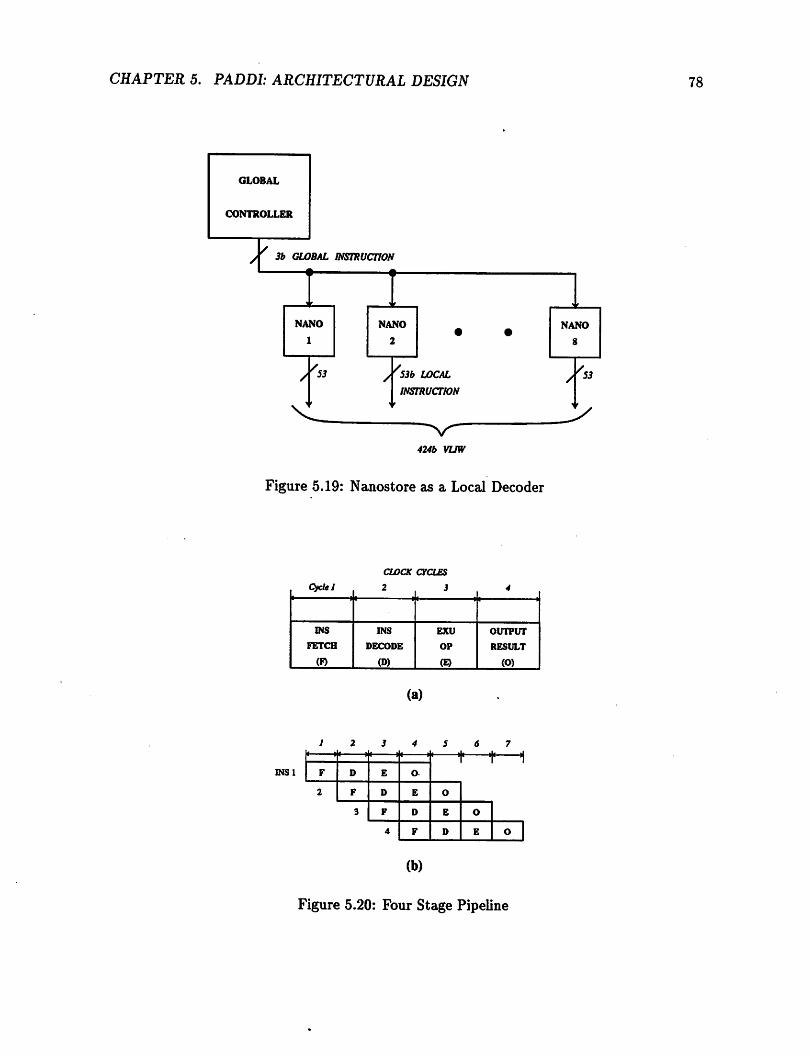
CHAPTER 5. PADDI: ARCHITECTURAL DESIGN
GLOBAL
CONTROLLER
y/ 3b GLOBAL INSTRUCTION* • —•
1 1
NANO
1
NANO
2• •
NANO
8
y '53 /'S3b LOCAL /*INSTRUCTION
. • • Y
^N^
424b VUW
Figure 5.19: Nanostore as a Local Decoder
clock: cycles
Cycle I 2 J 4
INS
FETCH
(F)
INS
DECODE
0»
EXU
OP
(E)
OUTPUT
RESULT
(O)
INSl
(a)
; 2 J 4 5 6 7
i ir .,-
F D E O
2 F D E 0
3 F D E O
4 F D E O
(b)
Figure 5.20: Four Stage Pipeline
78

CHAPTER 5. PADDI: ARCHITECTURAL DESIGN 79
EXUl F D E O
EXU 2
Figure 5.21: Local Delayed Branches
EXU registers. External memory is accessed by load and store instructions only, which are
handled by the external controller (Fig. 5.28).
Due to the pipelined nature of the architecture, branches and loads must be ac
counted for. The delay slots which they introduce are exposed to the assembly languageprogrammer and to the compiler for optimization.
Delayed Branches: The architecture supports two types of branches local and
global. In the former type, any exu on the same chip can alter the control flow ofany other
EXU on the same chip after 1 delay slot, as shown in Fig. 5.21. The EXU being interrupted
sets one or both of its interrupt enable flags in the previous instruction. Upon receipt of an
interrupt, it vectors to one of two pre-compiled instructions (denoted as IVs, for interrupt
vectors) in the next cycle. The hardware implementation of this feature will be described
in the next chapter (the test example of a modulo three counter described in Section 6.7.2
of the next chapter, also uses this feature and the branch logic hardware which implements
this is described in Section 6.4.2 of the next chapter). If the EXU being interrupted resides
on a different chip, an additional branch delay slot is required. During global branches, an
EXU flags the external controller which can then alter the global control flow as shown in
Fig. 5.22. In this case, two branch delay slots are also required.
Load/Execution Alignment: Because of the four stage pipeline, there is a two

CHAPTER 5. PADDI: ARCHITECTURAL DESIGN 80
F D E 0
F D E o
F D E O
F D E 0
F D E 0r
Figure 5.22: Global Delayed Branches
slot delay between an instruction issue and its corresponding EXU OP. The external memory
load for that instruction must be issued (by the external controller) so that the operands
will be aligned with its EXU operation. If single cycle SRAM is used, the system designer
must insert an additional delay stage between the sram and the chip as shown in Fig. 5.23.
as:
Time per Cycle (T):
The time required to perform a single machine cycle is determined by such factors
Instruction access time: Global instructions are generated by a fast commer
cially available external programmable logic sequencer e.g. [17, 119] and broadcast to each
EXU. For the prototype chip these are three bits long.
Instruction decode time: At configuration time, the local controller for each
EXU is serially configured each with its own unique set of instructions. Each controller is
an sram containing eight words of fifty-three bits each. Due to the small size of the srams,
global instructions can be decoded in a very short time.
Instruction operation time: All instructions execute in a single cycle.
Architectural simplicity: The organization of the machine is streamlined to
wards high speed DSP applications. By focusing on the operations important to our needs,

CHAPTER 5. PADDI: ARCHITECTURAL DESIGN
INS INS EXU OUTPUT
FETCH DECODE OP RESULT
(F) (D) (E) (0)
ALIGNED 1LOAD DELAY OPERAND
81
Figure 5.23: Load/Execution Alignment
we were able to optimize a small number ofcritical EXU features which support those oper
ations e.g. fast addition, max-min, accumulation, branching, and flexible communications.
Discussion:
A basic choice was to use a von Neumann-like, statically scheduled architecture
vs. a data-flow one. An objection to the former approach is that pipeline initialization
requires special controller states (nano-words) which serve no other really useful function.
Also data merges into a given processor requires several controller states. In a data-driven
approach, an encoding into the data stream might indicate the validity of the data. Hence
processing would occur only on the existence of valid data. This would circumvent the
need for extraneous prologue code necessary for pipeline fills in the statically scheduledcase. Some mechanism would be required to deal with data merge conflicts when severalsources attempt to broadcast to a single receiver. Another choice was to use a synchronous
approach vs. an asynchronous one. An asynchronous approach would not suffer from clock
skew problems, but would incur overhead to support the necessary handshaking protocols.Which of these various approaches might yield better results still remains to be answered
and is the subject of active research (e.g. [131]).

CHAPTERS. PADDI: ARCHITECTURAL DESIGN 82
5.5.4 IO
The key requirement for i/o is that there should be wide i/o bandwidth (hundreds
ofMB/sec). Wide i/o bandwidth mainly refers to the communication of the processors with
the external world. Recalling that we have chosen a hierarchical interconnection approach,
we note that a wide i/o bandwidth is also desirable for on-chip inter-cluster communication.
This will facilitate the task of the compiler in mapping and scheduling operations which
need to communicate across clusters.
5.5.5 Memory
Since the applications that weintend to support are data path intensive, a decision
was made not to explicitly support memory. There is someimplicit memorysupport. Every
EXU has a register file connected to both its input ports. These register files allow for a
temporary data buffering, which can alleviate the contention problem on the interconnect
buses. If larger amountsof memory such as video delay lines and frame buffers are required,
these will be implemented as external (commercially available) components in the finalsystem.
5.5.6 Configuration
Design Considerations
The configuration module must do whatever is necessary to configure the archi
tecture before run-time. The major issues were whether or not to have on-chip support for
automatic configuration, how to interface with slow external boot memory. It was finally
decided to include an on-chip configuration module which could interface seamlessly to an
external boot eprom without the need for additional glue logic. The hardware design of
these modules will be described in the next chapter.
At another level, weneeded to decide which configuration information wasrequired
to be in the control store and thereforeunder run-time control, and which could be statically
defined. The former is more costly in silicon area because it increases the size of the control
store,whereas the latter canbestored more cheaply in the serial configuration scan registers.
Appendix C lists the final choices that were made.

CHAPTER 5. PADDI: ARCHITECTURAL DESIGN 83
5.6 Processor Summary
The final overall architecture is outlined in Fig. 5.24. It contains thirty-two exus,
organized into four clusters (or quadrants) ofeight exus each. Quadrants are organized in
a ring network. The exus in each cluster are fully connected by a dynamically configurable
crossbar. We envision a family of processors using this architecture. The main difference
between the different processors shown is the number of exus per processor. Two members
of the family are shown in Fig. 5.25 and Fig. 5.26. Additionally, the number of words in the
instruction store and the basic functions of the EXUs can be varied to provide new members
of the family. For example, Fig. 5.27 shows a modified architecture with two multipliersshared over six EXUs. Another design might share one multiplier over seven EXUs, dependingon the demands of the applications. The level ofpipelining in the multipliers could be variedto accommodate the level of sharing.
At this point, a word about resource balancing is appropriate. Assuming a 25
MHz operating frequency, the Peak Computation Rate to i/o ratio for a thirty-two EXU
processor is 800 Mops to 400 MB/sec or 2.0 Mops/MB/sec. This ratio is similar to the
geometric mean of3.56 Mops/MB/sec of the benchmark set. An MCM based approach' with
double the processors and similar i/o resources will make the ratios tend to converge evenfurther, if desired.
As a proof of concept the architecture shown in Fig. 5.26 was implemented as a
single VLSI component. Its hardware implementation will be described in Chapter 6.
Fig. 5.28 shows how the chips might be applied in a simple system. At power up,
the paddi chips (labeled pads) are configured by self-booting from the boot ROM. After
receiving a startsignal from the externalcontroller, the chips are able to perform both data
computation and memory addressing tasks. The external controller determines the global
instruction sequence and issues the appropriate loads and stores to external memory. (The
figure shows a pad being used as an address generation unit (agu)). Flags generated fromthe pads (and theexternal world) can be monitored to effect global branching.
5.6.1 Benchmarks
Appendix B contains a list of benchmarks that were hand compiled to the paddi
architecture and exemplify how the mapping is done.

CHAPTER 5. PADDI: ARCHITECTURAL DESIGN
r tt t ~^r "^r "y "^ ^
SiI/O
SWITCH w SWITCH
I £ £ £ £
aT T T"T IT T I
SWITCH
ET3w SWITCH
I/O
ETUI LJLtt
Figure 5.24: PADDI with 32 EXUs
4
4
4
r t T"iSWITCH
JL _JL _JL _Jt
I
I
i
1 3T ItSWITCH
II
I
I
ITZ3
Figure 5.25: PADDI with 16 EXUs
I/O
:i:
£
I/O
84

CHAPTER 5. PADDI: ARCHITECTURAL DESIGN
I/O
TH EXUL
"ZST
_sk
EXU
C •»
T •» EXU
5Z
SWITCH
SZ
EXU
EXU
C *
T * EXU
L *
r t
•zp
EXU
IC *
T •» EXU
L •»
Figure 5.26: Prototype Architecture
EXU
ZT
SZ
SWITCH
EXU
MX
_sz_
IMX
Figure 5.27: Prototype Architecture With Multipliers
85
I/O
I/O

CHAPTER 5. PADDI: ARCHITECTURAL DESIGN
DATA
INA/D
BOOT
ROM
CONTROL
PAD3
AGU
' PAD1
MEM
PAD2 * D/A
MEM
DATA
OUT
86
Figure 5.28: System Using PADDI Chips
5.7 Instruction Set Summary
A detailed description of the paddi instruction set is given in Appendix C.
5.8 Programmer's View
Appendix C provides an overview of the architecture as seen by the assembly
language programmer. The formats of the run-time instructions as well as the configuration
specifiers are presented there. A sample assembly program that contains instances of the
basic instructions, together with explanatory comments, is also presented.
Section 7.2.1 of Chapter 7 and Appendix G describe the annotated grammar that
was developed for the assembly language.
A description of the software environment and a discussion of the compiler issues
will be presented in Chapter 7.
5.9 Summary and Conclusions
We have presented the architecture of a software-configurable multi-processor
which was developed to support the rapid prototyping of high speed data paths. The

CHAPTER 5. PADDI: ARCHITECTURAL DESIGN 87
design was driven by the results of analyzing a characteristic benchmark set. Various tech
niques from the domains of software-configurable and Rise architectures were employed to
achieve high performance. The general design philosophy was one of "keep it simple" for
speed and implementability, with as few constraints on the compiler as possible, in order
to enhance hardware utilization.

Chapter 6
PADDI: Hardware Design
Een graficus heeft in zijn wezen iets van een troubador.(A graphic artist has something of the troubador within him.)
— M Escher, Escher on Escher
6.1 Introduction
As a proof of concept, a prototype of the the architecture described in Chapter
5 was implemented as a multiprocessor ic [26] using VLSI technology. This chapter will
discuss the logic and VLSI implementation of the major units which comprise the chip.
In orderto maximize the probability of fabricating a functional chip, a conservative
approach to circuit design was taken wherever possible. Thus, a static design style was
chosen over a dynamic one. In some cases this meant trading off increased area, and some
speed, for improved noise margin and decreased susceptibility to clock skew. This also
meant the choice of a conventional and modest two-phase clocking scheme using external
clock generators over more elaborate methods involving multi-phase clocks with on-chip
analog phase-locked-loop generators. Additionally, special attention was paid to the routing
and metal layer width of critical signals (such as clocks) and power lines.
The functional and speed test results will be presented for the prototype circuit
which contains 8 execution units connected via a dynamically controlled crossbar switch. In
summary: it canoperateat 25MHz (200 mips) with a data i/o bandwidthof 400 MByte/sec
and a typical power consumption of 0.45 W. It contains 140,106 transistors on a 8.9 x 9.5
mm2 die, in 1.2 Lim CMOS technology.
88

CHAPTER 6. PADDI: HARDWARE DESIGN
-«BG-
HLE
1 I, 1
-raa-
I\«nm^-
r^^7
yt
fT
89
* WORDS
NANOSTORE
Figure 6.1: EXU Architecture
6.2 Execution Unit
A detailed block diagram of an EXU is shownin Fig. 6.1. This section will describe
the implementation of its major parts.
The adders wereimplemented using the carry-select-adder cells from the lageriv
cell library [64], the fastest available at the time. The adder consists of several stages thatwork in parallel to produce carry results for two cases: that of a zero carry input into the
stage and that of a one carry input into the stage. The true carry then ripples (stage-wise
not bit-wise) through the stages selecting the proper pre-computed carries, which are then
used to compute the sum at each bit. The successive stage lengths were chosen for optimal
speed. Starting from the least significant bit, these were three, five and eight respectively.
The shifters are capable of arithmetic right shifting from zero to seven bits, and
are implemented as a logarithmic shifter (Fig 6.2) using complementary pass transistor
gates. As mentioned previously, the exus can be user-configured to operate in 16b and
32b modes. Shifter interface logic ensures correct operation for both 16b and 32b modes of
operation, independent of whether the arithmetic is two's complement or unsigned.
Multiplexors are also implemented using complementary pass transistor logic.
The dual ported register-files and pipeline register at the output of each exu are
implemented using a static register cell for regular storage, and c2mos inverters for delay

CHAPTER 6. PADDI: HARDWARE DESIGN 90
WIS
sawn
SHIFT4
OUT1S ovro
IN A INB
J L
*—idfi2 4/JQE-f-HGya Jpfy)SHIFT
• SHIFT
OUT
Figure 6.2: Logarithmic Shifter
line mode. A detail of the register-file cell is shown in Fig 6.3. Register six of each register
file has the same basic structure as the other registers register. However it is linked to the
serial configuration scan chain by extra hardware and input and output ports. This feature
allows it to be set to an arbitrary value at Configuration time which is useful for setting
constants and initial values. This feature also enables it to be used during the Scan-Test
mode.
The exus contain hardware support for the max and MIN operations, and satu
ration logic for both unsigned and two's complement arithmetic. A status flag (a > 6) is
also provided. Correct operation is provided for both 16b and 32b modes. A detail of the
logic which implements this is shown in Fig 6.4. In this figure, the carry out bits from the
adder are used to generate two overflow bits, v2sc for two's complement mode and vun-
signed for unsigned mode. The choice of arithmetic mode is specified by the SUN bit which
is statically determined and set by the user. The saturation logic block uses these bits to
provide the correct saturated output (high or low) whenever an overflow or underflow is
detected, independent of the arithmetic mode. Other fields of interest are agebbar2sc and
agebbaru. The former is a flag which indicates that operand A is greater than B, assuming
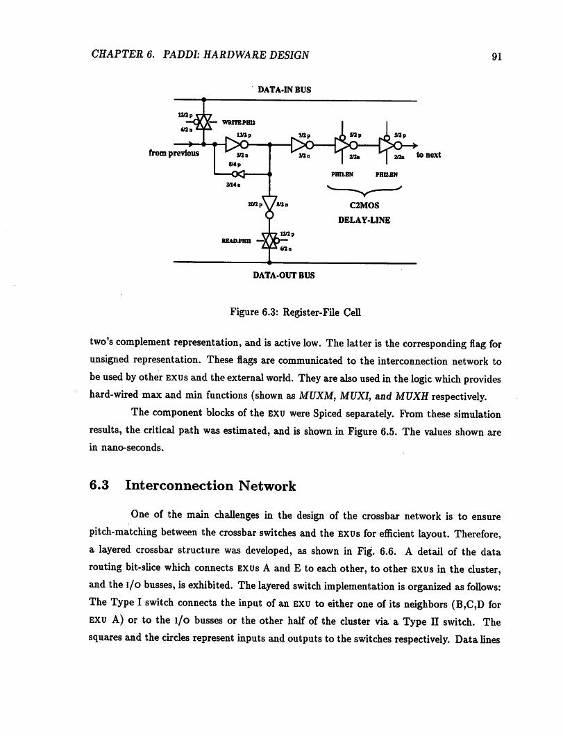
CHAPTER 6. PADDI: HARDWARE DESIGN
from previous
DATA-IN BUS
W2p\/a/2p
12/2 pRBAD-PHD —XX)—
UK
C2M0S
DELAY-LINE
2/2o to next
PHILEN PHOEN
91
DATA-OUT BUS
Figure 6.3: Register-File Cell
two's complement representation, and is active low. The latter is the corresponding flag for
unsigned representation. These flags are communicated to the interconnection network to
be used by other exus and the external world. They are also used in the logic which provides
hard-wired max and min functions (shown as MUXM, MUXI, and MUXH respectively.
The component blocks of the EXU were Spiced separately. From these simulation
results, the critical path was estimated, and is shown in Figure 6.5. The values shown are
in nano-seconds.
6.3 Interconnection Network
One of the main challenges in the design of the crossbar network is to ensure
pitch-matching between the crossbar switches and the EXUs for efficient layout. Therefore,
a layered crossbar structure was developed, as shown in Fig. 6.6. A detail of the data
routing bit-slice which connects EXUs A and E to each other, to other EXUs in the cluster,
and the i/o busses, is exhibited. The layered switch implementation is organized as follows:
The Type I switch connects the input of an EXU to either one of its neighbors (B,C,D for
EXU A) or to the i/o busses or the other half of the cluster via a Type II switch. The
squares and the circles represent inputs andoutputs to the switches respectively. Datalines
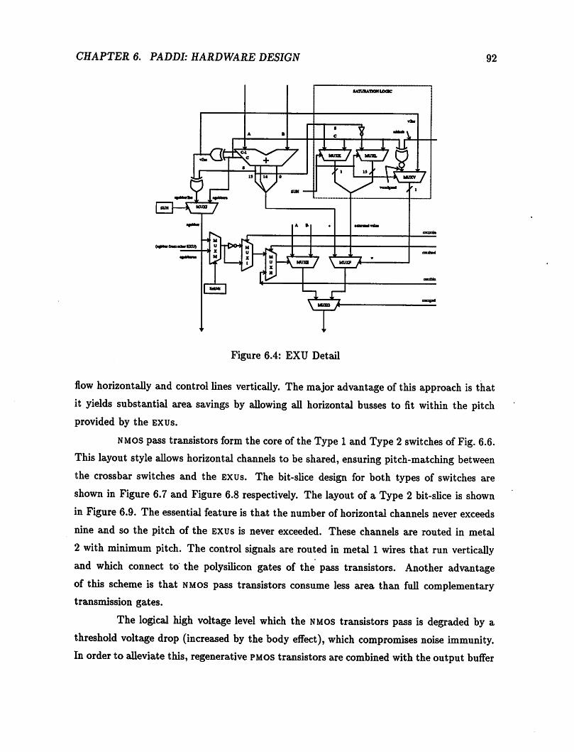
CHAPTER 6. PADDI: HARDWARE DESIGN 92
Figure 6.4: EXU Detail
flow horizontally and control lines vertically. The major advantage of this approach is that
it yields substantial area savings by allowing all horizontal busses to fit within the pitch
provided by the exus.
nmos pass transistors form the coreof the Type 1 and Type 2 switches of Fig. 6.6.
This layout style allows horizontal channels to be shared, ensuring pitch-matching between
the crossbar switches and the EXUs. The bit-slice design for both types of switches are
shown in Figure 6.7 and Figure 6.8 respectively. The layout of a Type 2 bit-slice is shown
in Figure 6.9. The essential feature is that the number of horizontal channels never exceeds
nine and so the pitch of the exus is never exceeded. These channels are routed in metal
2 with minimum pitch. The control signals are routed in metal 1 wires that run vertically
and which connect to the polysilicon gates of the pass transistors. Another advantage
of this scheme is that nmos pass transistors consume less area than full complementarytransmission gates.
The logical high voltage level which the nmos transistors pass is degraded by a
threshold voltage drop (increased by the body effect), which compromises noise immunity.
In order to alleviate this, regenerative PMOS transistors are combined with the output buffer

CHAPTER 6. PADDI: HARDWARE DESIGN
12 ns
^IY
\: MUX
^7
\ mux / \r ns
•KBG-
•fttS-
£
v-——* 7+ • 4.5 ns\ SHIFTER X|lqf
n ns
7 t" ns
Figure 6.5: EXU Critical Path
93
NANOSTORE

CHAPTER 6. PADDI: HARDWARE DESIGN 94
CROSSBAR SWITCH SCHEMATIC
O nttvr O ouirur
wnimui mr/anraimoohum MCTAIRTCB
Figure 6.6: Crossbar Network
h- h-
h h h h h
Figure 6.7: Type 1 Bit-slice

CHAPTER 6. PADDI: HARDWARE DESIGN 95
HI Hi HI HI HI HI HI HI
Figure 6.8: Type 2 Bit-slice
Figure 6.9: Layout of Type 2 Bit-slice

CHAPTER 6. PADDI: HARDWARE DESIGN 96
TYPB2SWITCH 4--> TYPB1SWITCH
•1 •1 r>
£*>tH»'
ir-HX>*r•1
i>>*t
Figure 6.10: Regenerative PMOS Design
stages of each switch to restore the output high voltage level to rail. The output buffer stages
are necessary to maintain sharp edges and speed. Types 1 and 2 switches were cascaded
directly as shown in Fig. 6.10 (the capacitance values shown are in femto-farads). The
design was coupled in order to avoid using extra buffer stages. This circuit was Spiced
for different W/L values of the regenerative pmos's and a few of the results are shown in
Fig. 6.11. Too weak aW/L causes an inordinately long restoration time. Too strong aW/L
inhibits the driving stage (Type 2), from ever pulling down the following stage (Type 1). A
W/L of 4/3 was chosen for the chip. The critical path through the network was simulated.
Imagine that there are two communicating quadrants. This path begins at the output of
an EXU in one quadrant (say EXU G in Fig. 6.6 which is input to the network. The path
continues through to the out bus into the IN bus of another quadrant, through Type 2 and
Type 1 switches, and is finally input to an EXU (say EXU D) of that quadrant. Such a path
is shown in Fig.6.12. The spice output (inverted) is shown in Fig.6.13. An average delay
of approximately 15 nsec. from input to output was measured.

CHAPTER 6. PADDI: HARDWARE DESIGN 97
TIME (NS)
Figure 6.11: Regenerative PMOS Design (Spice)
r T I r t t i$=$
i, „JL K * „JL „JL _JL i
2ns
r T T T T T T"t6ns $=$
i, „JL „JL „li- LJt f X 3
Figure 6.12: Interconnect Critical Path

CHAPTER 6. PADDI: HARDWARE DESIGN
VOLTS
j
input
4 -
3 •
2 •14.65
< *i
14.9 !
1 •output
\ l i 1 / 1
20 40 60
TIME (nsec)
80 100
98
Figure 6.13: Interconnect Critical Path Simulation
6.4 Control
This section describes the implementation of the nanostores which control the
EXUs. It also describes their associated branch logic which determine the flow of local
control streams.
6.4.1 Nanostore
The nanostores are implemented using an sram containing standard six transistor
sram cells. A bit-slice of the nanostore is detailed in Fig 6.14. A serial master-slave
scan-register, which is part of the global serial configuration scan chain, is connected to the
read/write ports of the sram. During Configuration mode, it is used to write the contents of
the srams word by word. At run-time, it is transparent as the SRAM issues each instructionword.
Each SRAM contains eight instruction words, each 51b wide. No column decoding
or column amplifiers are required for these small srams. They also have fast word accessesdue to their small size.
The associated control signal generation circuitry for the srams is shown in Fig.6.15. Buffers are sized to ensure minimal delay, sharp edges and proper timing of critical

CHAPTER 6. PADDI: HARDWARE DESIGN
SCAN-IN
SERIAL
MASTER-SLAVE
SCAN-REGISTER
INSTRUCTION-BIT
. 12U1
Utto
Figure 6.14: SRAM Detail
SCAN-OUT
BIT
! EQUALIZATION
99

CHAPTER 6. PADDI: HARDWARE DESIGN
.-jC,m •
in _ 4M
,?-t>-[>>-i>H>o-^>—r
^H>H>0-[>-u>-
^Oo-Oo-Cxj-IX)—4~V>o
IQUAIXUTXM
CH)
100
.EKAIU
Figure 6.15: SRAM Control Circuitry
signals.
The timing diagram of the sram is shown in Fig. 6.16. The sram operates using
the same two phase clocks PHll and PHI2 that are used throughout the rest of the chip.
Using this methodology, addresses are latched on the falling edge of PHI2 and read data
is latched on the falling edge of PHll. The read (/r) and write (/w) signals are active
low. Special attention was paid to ensure that word lines (wl) did not glitch due to chargesharing effects in the row decode circuitry. The bit-line and inverted bit-lines are denoted
by (b) and (/b). The pre-amp enable is denoted by pe and the write enable is denoted bywe. The data-out line is denoted by do and the datain line by di. A spice simulation of
the critical path during reading is shown in Fig. 6.17. The reading and writing times ofthe sram is not an issue because the size of the sram is quite small. A read access time of
approximately 21 nsec. is observed.
6.4.2 Branch Logic
The branch logic is shown in Fig. 6.18. It controls which nano addresses are sent
to the nanostores during the various phases of operation. During configuration, the nanoaddress is set by the Configuration Unit, independent of the interrupt flags and interruptenables (which are indeterminate during configuration). At run time, the nano address may

CHAPTER 6. PADDI: HARDWARE DESIGN
I
Ml |i
11ij 1-
11
1 11I
1ii
1
!
11
iI
P<
i
!
i
1 1
1111
i
!
i
{
11 ! i
i 11
1 i I1 i !
HHQ 1
1
! . 1 | |i i !1 ! i
~^ Y j j mnlaiwi I j wfniAri i
* X y$mi
! 1 1i ! j i
j
i
1 |i 1
[i 1 ! !
i • i
A I !
\
! ij j
i ii I! !
. i !i |
ii
1 1 !1 i i
i i ii i 1
|i ; ;
/» !
Wl
1 i i
/ 1 i I"i
1 i! !i i
j i i
1 ! '
<•
•tan <
i
1/
! j
1VM.
1 !
\
1 '- ^i
tcooc ML \
|1
WLI
/
i i !
"• 1
i
\ii! \
! !i i
IIS
! / ! \ | 1 1 1
*• ! 1|
/
i
i
1 1 1
_ _ jV V
i
i
i
^\
/1 !
ii
i i j
^ i i i ! 'S1 |i i
j i ! i
"S>^ X ; iaptttdau k x8>cy!
i 1 i! ! i
i j |
\
!
i 1
-W£<;X/i l\ diavtU /! •
j
Figure 6.16: SRAM Timing Diagram
101
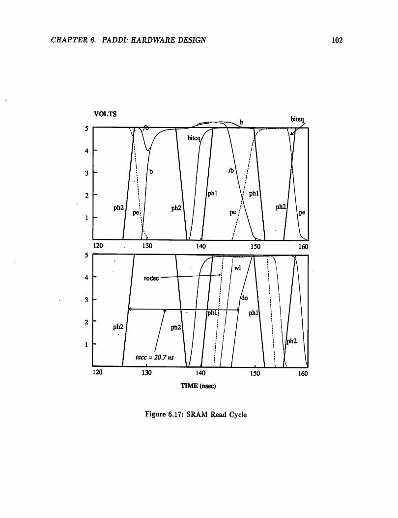
CHAPTER 6. PADDI: HARDWARE DESIGN
VOLTS
140
TIME (nsec)
Figure 6.17: SRAM Read Cycle
102

CHAPTER 6. PADDI: HARDWARE DESIGN 103
INPUT ADDRESS
SNOP <H^1tI>0^>>SYNC
Figure 6.18: Branch Logic
come from one of three sources. In the normal flow of operation, the usual source is is the
address generated by the external microsequencer. However, depending on the values of the
interrupt flags and interrupt enables it may also come from one of two (serially configured)
interrupt vectors (IV1, IV2). Synchronization between the configuration and run phases is
enabled by the snop and sync signals. The snop signal is asserted whenever a stop signal is
received from the external sequencer, or whenever a nop is received from the configuration
unit during configuration and verification phases.
A conventional non-overlapping two phase clocking scheme was used in the proto
type chip. A diagram showing how the various latches in the processor are clocked is shown
in Figure 6.19. This diagram shows two exus, A and B which communicate with each
other and the external world. Data-in, flag-in, global-addr and stop are input from the
external world. The input pads are contain half-latches which are clocked with PHll. The
global-addr is routed to the Branch Logic Module (BRL) the output of which is latched
on PHI2 as the address to the nano-store. The register files of exu are read at the beginning
of PHll and results are latched at the end of PHI2. In this figure, EXUA can be interrupted
from the external world and exuB depending on the status of the interrupt enables (IENl
and IEN2. exuB can be interrupted by EXUA. In general output data is latched at the
output pads on PHI2 and output flags are latched on PHll as shown for exuB. In this way,

CHAPTER 6. PADDI: HARDWARE DESIGN 104
paddi chips can be directly cascaded with an effective pipeline stage connecting the input
pins.
6.5 Configuration Unit
The Configuration Unit provides the requisite signals which allows the chip to
automatically self-boot from an external memory e.g an eprom. It enables the chip to
temporarily suspend operations, to verify the nanostore contents, and perform scan-testing
of the exus and interconnection network.
All chip configuration registers are connected as a serial shift register. This serial
shift register is also connected to the i/o circuitry of the SRAMs. The Configuration Unit
is composed of two on board fsms which generate the necessary clock and interface and
internal control signals for the external eprom, the serial shift register, and the srams.
6.5.1 Modes of operation
The Configuration Unit provides several modes of operation for the chip: a) Configuration, b) Stop, c) Run, d) Test.
Upon receipt of the appropriate boot signal (start), the chip enters Configuration
Mode. During Configuration Mode a complete line-scan is performed, then a location of
the nanostores are written via sections of the scan-chain which connect to the i/o circuitryof the srams. (A description of the scan-chain is given in below). This repeats until all
nanostore locations are written. The final scan is left in place to configure the rest of thechip.
During Stop Mode, the chip has been properly configured (or was running), but is
awaiting a go signal from the external controller before proceeding to Run mode. After the
chip has been properly configured, and has received the GO signal at its input pin it enters
Run Mode. In this mode, normal operation proceeds until the go signal is de-asserted (orthe chip is re-booted).
Test Mode will be described in Section 6.6.

CHAPTER 6. PADDI: HARDWARE DESIGN
data-in
data-out
global
flag-in adr stop
pi-6-th-A
Figure 6.19: Clocking of State Latches
105

CHAPTER 6. PADDI: HARDWARE DESIGN 106
Scan Chain
Fig. 6.20 shows a section of the scan chain connecting two EXUs. Cona, conb, and
oreg are scan registers which are used to set constants, and which can be overwritten at run
time. Statically defined configuration bits include: Linkwhich determines 16-bit or 32-bit
exu mode, sun which sets two's complement or unsigned arithmetic mode. Nvec which
contains pre-compiled interrupt vectors, and fswl and fsw2 which determine the routingof
status flags. Ftridetermines output bus selection. Nanostores are configured via the nanoregister.
The exu instructions and data routing are under program control and can be
changed in each program cycle. The routing of the status flags is static and set at compiletime.
6.5.2 Finite State Machines
In this section the constituent finite state machines which make up the Configuration Unit will be described.
By using a simple 3b counter, FSMl (cf. Fig. 6.21) slower non-oveflapping, two-
phase clocks (phim and phis) which are slower than PHll and PHI2 (the normal operatingclocks of the chip), and which are synchronized to PHI2 (Fig. 6.22). Slower clocks allow
interfacing to eproms which operate at slower (lOx) speeds than the operating speed (25MHz) ofour chip. Appendix D describes the various signals that interface with the externalboot-memory.
The main configuration tasksare performed by fsm2 which operateson the slower
clock frequency. After the start signal has been asserted and FSMl stabilized, startdel (adelayed version ofstart) is asserted and fsm2 enters Configuration mode. A line counter
(lctr) keeps track of the scan into the serial configuration scan-chain. A frame counter(fctr) keeps track of which nanostore word is currently being written (or read).
Multiplexors ensure that correct values are set for scan and addr respectivelyduring each mode of operation, scan is combined with clocks phim and phis for clockingthe serial configuration scan-chain. ADDR is broadcast to the Branch Logic Units of allEXUs. It is de-multiplexed from frame cnt and EXT addr. frame cnt provides theappropriate address for writing during Configuration Mode, ext addr is sourced from the
external world, usually from the external microsequencer.

CHAPTER 6. PADDI: HARDWARE DESIGN 107
Figure 6.20: Section of Configuration Scan Chain

CHAPTER 6. PADDI: HARDWARE DESIGN
PHI1
PHI2
PHM
PHS
PH2-
START -
COUT
FSMl
7R *
*—*
LD
EN♦ y
•- 3b CTR
Figure 6.21: FSMl
* w
Y Y
PHI
PH2
PHM
PHS
Figure 6.22: PHIM and PHIM Clock Generation
108
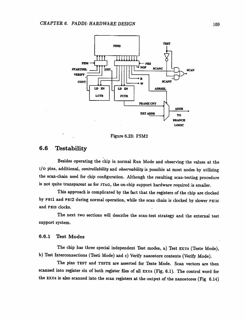
CHAPTER 6. PADDI: HARDWARE DESIGN
PHM
STARTDEL
VERIFY
COOT
6.6 Testability
LD EN
LCTR
FSM2TEST
*******
LD EN
FCTR
i—PHS
NOP SCANC
•+R
•+WSCANT
ADRSEL
FRAME CNT
EXTADDR
ADDR
TO
BRANCH
LOGIC
Figure 6.23: FSM2
109
SCAN
Besides operating the chip in normal Run Mode and observing the values at the
i/o pins, additional, controllability and observability is possible at most nodes by utilizingthe scan-chain used for chip configuration. Although the resulting scan-testing procedureis not quite transparent as for jtag, the on-chip support hardware required is smaller.
This approach is complicated by the fact that the registers of the chip are clocked
by phi1 and PHI2 during normal operation, while the scan chain is clocked by slower phimand phis clocks.
The next two sections will describe the scan-test strategy and the external testsupport system.
6.6.1 Test Modes
The chip has three special independent Test modes, a) Test EXUs (Teste Mode),b) Test Interconnections (Testi Mode) and c) Verify nanostore contents (Verify Mode).
The pins test and teste are asserted for Teste Mode. Scan vectors are then
scanned into register six of both register files of all exus (Fig. 6.1). The control word forthe EXUs is also scanned into the scan registers at theoutput of the nanostores (Fig 6.14)

CHAPTER 6. PADDI: HARDWARE DESIGN 110
of Section 6.4.1. For one (long) clock cycle, the exus operate normally, after which the
results are latched in the output pipeline register (Fig. 6.1) and scanned out.
The pins test and testi are asserted for Testi Mode. Scan vectors are then
scanned into the output pipeline registers of all EXUs (Fig. 6.1). The control word which
specifies the routing of data through the crossbar switch is also scanned into the scan
registers at the output of the nanostores (Fig 6.14). For one (long) clock cycle, the data
in the pipeline registers are propagated through the switch, latched into register six of the
target exus, and scanned out.
At any time after Configuration, the chip can receive a verify signal which will
force it into the Verify Mode. In this mode, a word of the nanostores is read, and scanned
out. This repeats for all nanostore words, thus enabling verification of the nanostore con
tents.
6.6.2 Test Support System
A pre-existing Test Support System [61], (Fig. 6.24), was retro-fitted to accom
modate the specific requirements of the chip. The system allows the user to download
scan-test vectors from a SUN workstation to a Test Control Board (tcb) which is connected
to the Device Under Test (dut). The architecture of the Test Control Board is shown
in Fig. 6.25. It is comprised of the vme interface which connects it to the backplanes (Jl
and J2), the vme interface logic (a VME2000) which implements the protocols that meet the
VMEbus specification IEEE 1014 timing requirements, control, status, and data registers, the
Test Controller, test data memory (scanin and scanout memories), the address counter
which generates the addresses for the test data memory, and the analog, scan-path, and
TAP interfaces, which connect the TCB to the duts.
The main change to the architecture was made in the Test Controller. This which
was implemented using EPLD's and so the changes were essentially software ones. The
design of the new test control board was completed but it was never fully implemented,
because the chips were tested (in Run Mode) and found to be completely functional, before
its hardware implementation was completed.

CHAPTER 6. PADDI: HARDWARE DESIGN
SUN (UNIX)
Ethernet
VME
CARD
CAGE
ImpUjitaaTtsCBtg
TCB
CPU
BOARD
*
Test Bus
jt&worktnf endCentmuminMiem
VME Bus* •
DUT
Figure 6.24: Test Support System
VME
Interface
Logic
Local Bus
Test
ControDer
VME Interface
Local Test Bus
Test Interface
TcstDate
Memory
Address
Counter
Figure 6.25: TCB Architecture
111

CHAPTER 6. PADDI: HARDWARE DESIGN
H»
mnr V*mn
PHU ~^0-^»
4»
Figure 6.26: Clock Distribution
6.7 Clocking
tfMP
"—0^~ PHDUMH
112
A conventional non-overlapping two-phase clocking scheme was used in the proto
type chip. Clock distribution was facilitated by the identical nature of of the EXUs and the
symmetry of the layout. Fig. 6.26 shows how the clocks were routed from the input pads.
Drivers were sized to maintain sharp edges.
6.7.1 Layout and Simulation
Layout: Hand-crafted cells were laid out using the MAGIC cad tool [90]. The
carry-select adder cells were obtained from the Lager cell library [64]. A micro-photograph
of the chip is shown in Fig. 6.27.
Simulation: Circuit and behavioral simulation were performed using spice [83]
and irsim [105] respectively, and the pas assembler was used to generate simulation test
vectors and chip configuration files. The configuration FSMs were described in a high level
behavioral language and their corresponding plas were automatically generated using the
Berkeley OCT tools [64].
SPICE simulations were performed to simulate the critical path of the chip. The
respective load capacitances wereestimated from the worst case ic process parameters and

CHAPTER 6. PADDI: HARDWARE DESIGN
nnDrnnnnnnn
H-"*- •*Mias)Ctiaaj<aM*CgiaM aiij^v^;-it n ~Kia**M«g=
' '-^-'i--J'-LLLLi_LLjLiUULiLjL;uUL'ULiL'IJUDUUUUUULJLJULjUdUUUUL}UL3DDu
Figure 6.27: Chip Photo
113

CHAPTER 6. PADDI: HARDWARE DESIGN
2 at
V ft t 24 ns
5=$
:L_ t ft ft1
6ns
<
1
II*
ft
ft
ft
ft
ft
ft
ft
ft
ft6ns
—ft
¥*! ft :?:l2 rS t
t
ft ft
Figure 6.28: Four Quadrant Critical Path
114
incorporated into the spice decks. The critical path simulation results for the EXU was
shown in in Fig. 6.5 and the critical path simulations for the interconnect network were
shown in Fig. 6.12. These results are combined to show the critical path simulation results
for a four quadrant chip (Fig. 6.28). The units shown are in nanoseconds. The critical
path begins from the issue of a read address to register file B. A delay of 24 nanoseconds is
incurred during EXU transit from the register file, through the shifter and inversion logic,
through the carry path of the carry select adder, through the saturation logic to the output
of the exu. An additional 15 nanoseconds is lost during transit through the crossbar
networks, after which 2 nanoseconds are required to latch the data into the input of the
target EXU. The total simulated critical delay is 41 nanoseconds.
We note that the prototype chip which contains a single quadrant runs at a maxi
mum clock frequency of 25 MHz with a critical path delay of 40 nanoseconds. This indicates
that there is excellent agreement with the SPICE simulations. The only major difference be
tween a single quadrant and one with four quadrants is the additional inter-quadrant transit
time which, with proper buffering, can be limited to 1 or 2 nanoseconds.
As was indicated in Section 5.5.1, a pipeline register is available at the output
of each exu for optional use. By using the register, the user can increase the maximum
sampling rate by overlapping EXU operations with data transmission over the network. This
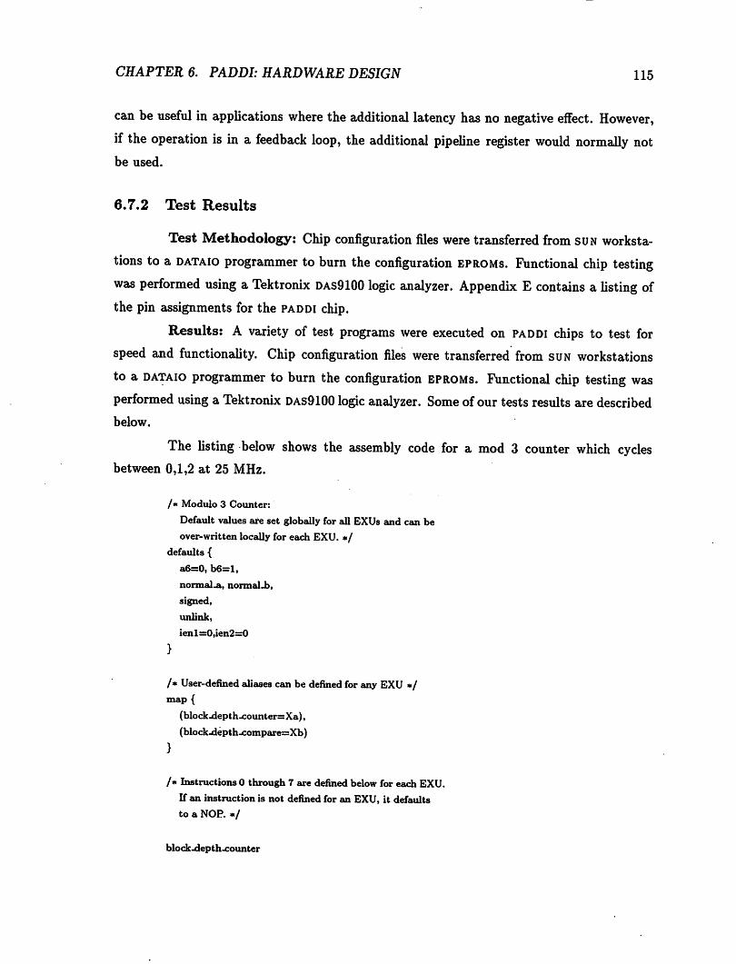
CHAPTER 6. PADDI: HARDWARE DESIGN 115
can be useful in applications where the additional latency has no negative effect. However,
if the operation is in a feedback loop, the additional pipeline register would normally notbe used.
6.7.2 Test Results
Test Methodology: Chip configuration files were transferred from sun worksta
tions to a dataio programmer to burn the configuration eproms. Functional chip testingwas performed using a Tektronix DAS9100 logic analyzer. Appendix E contains a listing ofthe pin assignments for the paddi chip.
Results: A variety of test programs were executed on paddi chips to test for
speed and functionality. Chip configuration files were transferred from sun workstations
to a DATAio programmer to burn the configuration EPROMs. Functional chip testing was
performed using a Tektronix DAS9100 logic analyzer. Some of our tests results are describedbelow.
The listing below shows the assembly code for a mod 3 counter which cyclesbetween 0,1,2 at 25 MHz.
/* Modulo 3 Counter:
Default values are set globally for all EXUs and can be
over-written locally for each EXU. */
defaults {
a6=0, b6=l,
normals, normal_b,
signed,
unlink,
ienl=0,ien2=0
}
/* User-defined aliases canbe defined for any EXU */map {
(block-depth-counter= Xa),
(block-depth-compare=Xb)
}
/* Instructions 0 through 7 are defined below for each EXU.
If an instruction is not defined for an EXU, it defaults
to a NOP. */
block-depth-counter

CHAPTER 6. PADDI: HARDWARE DESIGN 116
/* vector to instruction 1 when blockjdepth-compareasserts its flag */
flagl=blockjdepthjcompare, ivecl=l
{/* instruction 0: increment a6 by 1 and store the result
in a6 and bl, enable interrupt ienl, send result to
output bus ol */
0: a6=thisjexu, bl=this.exu, (a6+b6), ienl, ol;
/* instruction 1: subtract bl from a6 and store the result
in a6 and bl (this resets a6 and bl to zero), send
result to output bus 1 */
1: a6=this.exu, bl=this.exu, (a6-bl), ol;
}
blockjdepth-compare
a6=0,b6=0, /* overwrite global default values */
flagoutl=l /* route flag off-chipvia bus 1 (formonitoring) */
{
/* instruction 0: latch output of
blockjdepth-counter into register b6, subtract b6 from
a6. If b6 is greater than or equal to a6, assert flag.
Send result of a6-b6 to output bus o2 (for monitoring) */
0: b6=block-depth-counter, (a6-b6), o2;
}
The oscilloscope trace for the counter is shown in Fig. 6.29
The SFG of a low pass biquadratic filter is shown in Fig. 6.30. (It is the same one
referred to in Appendix A). The multiplying coefficients were converted to a canonic signed
digit format to minimize the number of non-zero bits and transformed into shifts and adds
(Fig. A.2). A processor schedule for this transformed SFG was hand-generated. It uses three
exus and three instructions andis shown in Fig. 6.31. The listing below shows the assembly
code for the biquad. Shown in Fig. 6.32 is the acquired impulse response (from a Tektronix
DAS9100), (a) a plot of the impulse response and (b) a plot of the corresponding frequency
response. The arithmetic mode is 16-bit two's complement and the impulse is input at bit
13. The measured results agree perfectly with simulations. Due to limitations of the signal
analyzer in acquiring data, the maximum clock rate of this biquad was constrained to 10
MHz.
/* Biquadratic Filter */
DEFAULTS {

CHAPTER 6. PADDI: HARDWARE DESIGN 117
A6 = 0, B6 = 0, SIGNED, UNLINK,
NORMAL-A, NORMAL.B,
BFSW = 11111111b,
IEN1 = 0, IEN2 = 0
}
MAP{
(EXU-A = XA),
(EXU-B = XB),
(EXU.C = Xc)
}
EXU-A {
1: (A6+(B6>4));
2: (B6);
3: A6 = I2L, B6 = EXU-A, (A6);
}
EXU_B{
1: A4=EXU-A, (A6+(B6>2));
2: B6=EXU-A, (A4+B6);
3: A6 = EXU.C, B6 = EXU.C, (B6);
}
EXU.C {
1: A2=EXU-B, B2=EXU.C, (A6-(B6>2));
2: A3=EXU-B, B3=EXU.C, (A2-B2);
3: A6=EXU-B, B6=EXU-C, (A3+B3),Ol;
}
Table 6.1 summarizes the chip characteristics.
6.8 Discussion
Given a more aggressive ic process, e.g. 0.8 /im, anda reasonably sized chip, a four
quadrant paddi chip each quadrant consisting of eight EXUs, is certainly implementable. In
order to illustrate this point we have tabulated several vsps [79, 107, 127] together with
the paddi chip in Table 6.2. The actual chip areas are listed. They are also normalized to
account for the difference in design rules. Two layers of metal were used in the fabrication
of all these processors. The ntt and Data-Wave chips are relatively six and four time
larger than paddi. Clearly we can realistically expect four to six times the area occupied
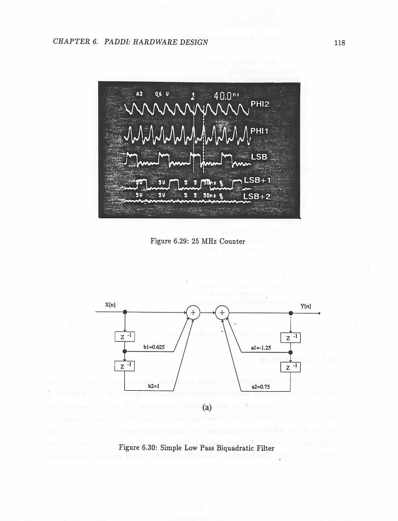
CHAPTER 6. PADDI: HARDWARE DESIGN
40.0
wwv\^^PHI2
PHM
TH 5u n 5 5 fib* * t^^8**B|iip*'i<' .i<U^~^«n ' \i,\***>**J l++++mJ- -£?+**> :3U 5U ': 5 5 30m \ LSB+2
Figure 6.29: 25 MHz Counter
X[n]
—I •—
b 1=0.625
—H
z-1
i
b2=l
Z"1
+
(a)
Y[n]
\ -
( >— •
Z'1
\ \ al=-1.25>
\
z-1
\ a2=0.75
Figure 6.30: Simple Low Pass Biquadratic Filter
118

CHAPTER 6. PADDI: HARDWARE DESIGN 119
AMPLITUDE
-0.5 -
INS
EXU A EXUB EXUC
•3 b3
Figure 6.31: Biquad Processor Schedule
GAIN (DB)
10.0 / \
0.0
-10.0
-20.0
-30.0
-40.0
I
75
TIME (300 nsec)
0.0 0.8
FREQUENCY (MHz)
1.6
Figure 6.32: Biquad Impulse Response

CHAPTER 6. PADDI: HARDWARE DESIGN
EXUs 8 units
16-32 bits
Register Files 2 files,
Six 16 bit registers
Nanostores 53 bits
8 words
I/O Ports 128
Clock Frequency 25 MHz.
Compute Power 200 Mips
I/O Bandwidth 400 MBytes/sec
No. of Transistors 140,106
Die Size 8.8x9.5 sq.mm
Table 6.1: Chip Characteristics
NTT VSP Data Wave Philips VSP PADDI
Design Rule 0.8/im 0.8 /im 1.6 /mi 1.2 (imTechnology Bi-CMOS CMOS CMOS CMOS
Word Lengths 16-24b 12b 12b 16-32b
No. transistors 910k 1.2M 206k 140k
Area (mm2) 15.2 x 15.2 12.5 x 12.5 9.9 x 12,3 8.9x9;5
Normalized area 6.15 4 0.81 1
Table 6.2: Chip Comparison of Technologies and Areas
120
by the prototype paddi chip. This will translate directly to four to six time the current
peak computation rate, to the first order. We also expect the performance of the chip to
improve with a scaled technology, especially if a BI-CMOS process is used.
One obvious way to increase the compute power of the paddi architecture is to
increase the number of EXUs on a single chip. Another is to employ an MCM based approach
usings sets of prototype chips. Both methodologies arebeing considered as future extensions
to the project, at the time of writing.
The crossbar switch in the paddi chip occupies exactly eighteen percent of chip
area. The design wasthe most efficient oneavailable to the author at the time. In the Philips
vsp the crossbar occupies less than five percent of the total chip area. At first glance, barring
any timing considerations, the VLSI design of the Philips crossbar switch seems superior to
that of paddi. This gives us reason to hope that, if the appropriate technology were to

CHAPTER 6. PADDI: HARDWARE DESIGN 121
become available, the size of the paddi crossbar could be shrunk dramatically.
6.9 Conclusions
The hardware implementation of a reconfigurable multiprocessor ic for rapid pro
totyping of real time data paths has been described. The chip is targeted towards high
performance digital signal processing applications* A 16 EXU (400 mips) processor is cur
rently under design, together with a multi-chip module approach which could support up
to 32 EXUs (800 mips) in a single package.

Chapter 7
PADDI: Software Environment
A slash symbol was usedsimply because the -r symbol wasnot a character on the 026keypunch.Similarly, the asterisk was used forexplicit multiplication because the x and • were not availableon the keypunch.
— M. Klerer on FORTRAN, Design of Very High-Level Computer Languages
7.1 Introduction
The major obstacle for the adoption of new programmable hardware platforms is
usually the lack of efficient and fast cad support tools. Therefore, from the inception of the
paddi project, special attention has been paid to developing cad tools which will enable a
mapping from high level language onto paddi.
In this section we will describe the grammar, assembler and simulator which have
been developed to enable user assembly language programming of paddi. Methods which
use high level synthesis techniques, to compile an abstract behavioral description of an
algorithm into these programmable arithmetic devices will be discussed. We will examine
the specific features of the architecture which will affect the quality of the compilation. The
cad environment and software tools being developed for automatic compilation from a high
level language [91] will be discussed.
7.2 Low-level Programming Tools
The low-level programming tools, the pas assembler and psim simulator, provide
the foundation for the higher-level synthesis tools.
122

CHAPTER 7. PADDI: SOFTWARE ENVIRONMENT 123
7.2.1 The pas assembler
Pas represents the lowest software level interface between the programmer and
the paddi architecture, providing a method for describing algorithms. The pas assembly
language was designed and implemented with the interconnection network of the paddi
architecture in mind: programs written in it can easily exploit intercommunication between
execution units. The intercommunication follows a "receiver controlled" model in which the
receiving unit controls the routing of the actual communication while the broadcasting unit
only concerns itselfwith the data or flag to be communicated (except when broadcasting to
the external world; in this case the broadcaster must specify which output bus to employ).
In addition to being able to express all available PADDI operations in a convenient c-like
syntax, the assembler also allows for the explicit specification of instructions within the
nanostores at the individual bit level. A detailed manual page for the assembler is listed in
Appendix F.
An annotated grammar for the assembly language is contained in Appendix G.
7.2.2 The psim simulator
Psim serves as a tool for simulatingand debugging multiple chip paddi algorithms
in software. It consists of a simulation engine coupled with an x-based graphical user
interface (gui). (see Fig. H.l) in Appendix H. The simulation engine can operate both
as a "black box," allowing it to interface with external software tools, or as a stand-alone
simulation environment when coupled with the x-based GUI. The stand-alone simulation
environment supports many of the common debugging features, including single-stepped
execution and the ability to modify registers and instructions "on the fly." A detailed
manual page for the simulator is also listed in Appendix H.
7.3 High Level Synthesis for Programmable Arithmetic De
vices
The success of an architecture depends heavily upon its ease of usage or ease of
programming. We are therefore interested in methods to compile an abstract behavioral
description of an algorithm into programmable arithmetic devices.
High level synthesis techniques can be brought to bear on the compilation problem.

CHAPTER 7. PADDI: SOFTWARE ENVIRONMENT 124
In high level synthesis, basic interdependent tasks which must be done include translation of
the high level language into an internal representation (typically some variation of a graph
with control flow and data flow constructs), transformations (at all levels of the process)
[124, 102, 89] scheduling, allocation, assignment, as described in [74] Various approachesdiffer in manner and the order in which these basic tasks are attacked.
In one approach, scheduling, allocation and assignment are performed separately
and in separate phases. The advantage of this approach is that it makes the problem some
what more tractable, because the different tasks are decoupled and solved independently.
The disadvantage of the approach is that it could yield sub-optimal results since decisions
chosenin one phase can have significant negative impact on the results obtained in another.
In another approach, for example the approach taken in hyper [98, 99], a global
optimization routine simultaneously takes into consideration all these tasks. Here the prob
lem is harder than the previous one.. A decision was made to adopt this type of approach
mainly because of the availability of the installed hyper software base, and the potential
for superior results.
We will begin by describing some of the architectural constraints of the paddi
architecture which will affect the compiler. We will then describe the two approaches to
compilation. In the first we will examine in detail a proposal for allocation and assignment
problem using a hierarchical clustering scheme. We will also discuss the latter approach
though somewhat briefly. The details of this approach will appear in [23].
7.3.1 Architectural Constraints
The goal is to identify computationally efficient means of compiling a high level
behavioral specification of an algorithm into paddi, subject to its particular hardware constraints.
A strong point of the architecture is the power of the cross-bar switch. It alleviates
much of the burden on the compiler since there are no conflicts when data routing is beingperformed inside a cluster of EXUs.
At this point we recall that the paddi chip will have clusters (or quadrants) of
eight EXUs. The term "quadrant" is adopted because the prototype architecture of EXUs
is one quarter of the original design, connected by a configurable crossbar switch. These
quadrants can communicate with each other but in a restricted fashion. The maximum i/o

CHAPTER 7. PADDI: SOFTWARE ENVIRONMENT 125
bandwidth ofthe chip is limited by thefixed number ofi/o pins. Each EXU has two registerfiles at its inputs, and is controlled by its own local memory (nanostore) to perform a setof basic operations. Each nanostore is in turn sequenced by the off-chip controller.
The ultimate goal of the synthesis process is to map the high-level description
onto paddi. This is achieved by generating the controlling sequence of nano-instructions
for each EXU. We will now discuss specific features of the architecture which will affect this
compilation process.
The system throughput requirements and the maximum clock frequency will de
termine the maximum level of hardware resource sharing as follows. The repetitive kernelin an (or in a part of an) algorithm is the smallest coherent part of the algorithm whichis repeated again and again in time, and which covers all arithmetic operations [42]. Ifthe rate at which the kernel has to be evaluated is /* and the operating clock frequency isfclocki then the hardware sharing ratio (hsr ) is:
HSR = ^jjj*
This sets an upper bound on the maximum number ofoperators which can be mapped to asingle EXU. The maximum hardware sharing ratio is constrained by two parameters. Thefirst is. the maximum number of registers in the exu's. In the prototype architecture this is
six. The register storage required for operands in the set ofoperations that get mapped toa particular EXU must not exceed this limit. The second is the number of instruction words
contained in the nanostore (eight in the prototype architecture). The maximum number of
unique operations that any given EXU can perform is set by this number. We note that, atthe cost of additional hardware, the number of registers and nanostoresize can be varied for
other members ofthe chip-set depending upon the performance range targeted. In general,it is desirable to pack as many operations intoas few EXUs as possible to maximize hardwareutilization.
7.3.2 Hardware Assignment Using Clustering
We will now examine the first approach to the compilation process i.e. where
the tasks of allocation and assignment are de-coupled from scheduling. In this approach,allocation and assignment will precede scheduling. Since much prior work has been done
on scheduling, we will address the allocation and assignment problem only. For example,

CHAPTER 7. PADDI: SOFTWARE ENVIRONMENT 126
we are considering the use of the hyper system scheduler as a candidate scheduler, hyper
is a high level synthesis system for real time applications.
Hierarchical Two Phase Clustering
We proposea hierarchical clustering approach to attack the allocation and assign
ment problem. In the following discussion, we restrict the problem size to one that will fit
on a single chip. One performs initial estimations to see whether or not the problem can fit
on a single ship. The multi-chip problem is subject to future research.
Clustering begins with EXU clustering followed by quadrant clustering. The ob
jective of EXU clustering is to pack as many operators into each exu as possible without
violating the hardware constraints. Quadrant clustering is clustering of the EXU clusters
with the goal of packing as many exu clusters as possible in each quadrant. Each type
of clustering uses the same algorithm and contains two phases, an initial solution phase
and an improvement phase. For each type of clustering, only the hardware and scheduling
constraints are different. Prior to clustering, weenvision a pre-optimization stage where sep
arate operations such as shift followed by an add, and add-compare-select can be collapsed
into a single operation to take advantage of the native instructions of the architecture.
We will now describe the initial and improvement phases which are generic to both
types of clustering.
Initial Phase
In the initial phase of clustering an attempt can be made to achieve a good first
guess. In many instances, the user will be able to easily identify obvious partitions where
there is a lot of local communication and from these partitions choose appropriate seed
nodes. Otherwise heuristics could be developed, to help guide the choice of the seed nodes.
When a node is attached to a seed node or another assigned node it is said to be assigned.
At each step of the initial phase, an existing cluster will join with the closest unassigned
node. Closeness measures will be defined using heuristics and moves will be subject to
hardware and scheduling constraints. Seed nodes will not be coalesced since there is no
backtracking in this phase. This phase provides an initial solution which, although it is not
guaranteed to have a successful schedule, does have a high probability of being scheduled
by keeping the constraints hard.

CHAPTER 7. PADDI: SOFTWARE ENVIRONMENT 127
Improvement Phase
In the improvement phase, simulated annealing [60] is applied to improve theinitial solution. One or more of the hard bounds are relaxed and even bad moves are
probabilistically accepted. Since the granulatity of the problem is coarse, i.e. we work with
EXUs and quadrants, not gates ortransistors, the size ofthe problem will not be very large,and so simulated annealing should not be too expensive to use. The closeness measures
and hardware bounds are wired into the cost function. Moves are tried e.g. pairwise swaps,triplet permutation etc. If the cost function is expensive to evaluate, complicated moveswill not be tried. Here a cost function based upon the closeness criteria and architectural
constraints is constructed. After completion of the annealing schedule, the final solution is
compared with that of the initial feasible solution and the winner is selected.
Detailed EXU Clustering
Closeness measures can be constructed which would attempt to encourage theclustering ofoperators which share the same control flow. If two operators are in the same
path, theirclustering isencouraged, ifnot they would bediscouraged. Othermeasures would
encourage the clustering ofoperators which sharedata, in order to keep the communications
local. On the other hand we would like to exploit low level parallelism and force operatorsthat have to be executed in the same cycle into different EXUs. Similar closeness measures
for a different clustering scheme have been done in the aparty architectural partitionerused in a behavioral synthesis system under development at Carnegie Mellon University[122] Some rough scheduling might be necessary here in order to identify such operators.
We will now discuss constraints particular to the PADDI architecture.
1) Maximum number of available registers per EXU: these will be incorporatedinto the closeness and cost functions. An efficient mechanism for estimating the number of
registers need per cluster will be required. Such a mechanism already exists for the hypersystem.
2) Maximum resource sharing: is determined by throughput constraints, sets upperbound on the maximum number ofoperators which can be mapped onto any EXU. This isa hard bound.
3) Communication constraints : we note that the switch network connecting theEXUs within a quadrant is under program control, while the switches connecting to quad-

CHAPTER 7. PADDI: SOFTWARE ENVIRONMENT 128
rants and to off-chip.modules are statically configured. If one makes the simplifying (sub-
optimal) assumption that the switches connecting the EXUs are statically configured, then
the maximum allowed fan-in per EXU is 2 and the fan-out is 1, again hard bounds. Such
an assumption will make the job of the register estimator and ultimately the scheduler
easier but will probably lead to sub-optimal solutions. Clearly the approach of not mak
ing this assumption will exploit the true power of the conflict-free routing network. If the
assumption is not made, then the bound on the fan-in to any EXU will be the twice the
maximum resource sharing allowed. The fan-out will be exactly the same. This is because
the exu switching network and the EXUs share the same nanostore. In this case, a more
sophisticated register estimator and scheduling algorithm will be required.
During the initial phase of exu clustering, an initial "good" solution is constructed.
Here a goodsolution means one which has a highprobability ofsuccessful scheduling. In this
phase, the register bound is kept hard. Assuming the specification of suitable seed nodes,
clusters are built up by attaching closest unassigned nodes. If a candidate causes either
the register, operator, fan-in or fan-out bounds to be exceeded, it is said to be infeasible.
Addition of nodes into a particular cluster terminates when all candidates are infeasible. At
this point, the cluster is said to be saturated and an EXU is allocated to it. At this point, a
new seed can be created by assigning an operator connected to any of those in the saturated
cluster. EXU clustering continues until no unassigned operator exists. At this point, an exu
can be allocated for each cluster. A record is kept of this initial feasible solution for later
use.
The improvement phase of exu clustering attempts to improve upon the initial
feasible solution by application of simulated annealing, as described earlier.
Detailed Quadrant Clustering
. At this point, quadrant clusteringof the EXU clusters can proceed. The problem of
quadrant clustering is to map the assigned EXUs to quadrants such that the interconnection
constraints are satisfied. These clusters are fixed internally and will not be modified. Once
the specific hardware constraints are updated for this level, the same clustering algorithm is
employed. At the quadrant level, the fan-in and fan-out bounds and maximum number of
EXUs are set by the architecture. The register estimator will continue to play an important
role at this level of clustering.

CHAPTER 7. PADDI: SOFTWARE ENVIRONMENT 129
When clustering is finished, the assignment task is complete and the scheduler
takes over. If the scheduler is successful the compilation task is essentially done. If not,
then either the time constraint or the clustering of operators within EXUs will need to be
relaxed.
The clustering approach described above is one approach which can be considered
for hardware assignment.
7.3.3 CADDI Compiler
We will now discuss the second approach to compilation, the one used in the
CADDI compiler. This compiler is being developed as a part of the unified rapid prototyping
framework environment, which also includes the hyper and mcdas [49] systems. The
three systems share a common database structure, but each targets a different architecture:
CADDI targets programmable arithmetic devices, hyper, semicustom architectures, and.
MCDAS, multiple programmable processor architectures. Besides the common data structure
and several tools, CADDI shares with MCDAS and hyper the same fully modular software
organization. This makes it easy to add new tools or to modify existing tools.
An overview of the envisioned system is shown in Fig. 7.1. An automated com
pilation path from a high level dataflow language silage [91] to the PADDI chip, which
includes partitioning, scheduling, and code generation is forseen. caddi will be similar
to the approach [95] taken in hyper and will contain all steps required for compilationnamely allocation, assignment, and scheduling modules, followed by translation into assem
bly language and ultimately into a configuration file. In hyper the synthesis procedure
is implemented as a search process. From an initial solution, new solutions are proposed
by executing anumber of basic moves, such as adding or removing resources, changingthe time allocation for different subgraphs in the algorithm, or applying graph transforma
tions, hyper uses a single global quality measure, called resource allocation, to drive the
search process. Theallocation andassignment approach differs from the approach presented
above in that a modification ofthe rejectionless antivoter assignment algorithm of [95] isenvisioned.
Therapid prototyping framework will allow the designer toexperiment andanalyze
the speed vs. cost trade-off for various implementations as well as theeffects ofquantizationand transformations on system performance. Initial results and the on-going investigation
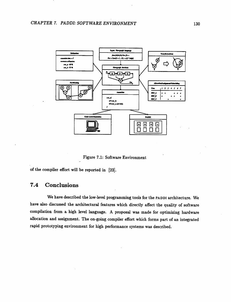
CHAPTER 7. PADDI: SOFTWARE ENVIRONMENT
BatMtoa
iimm'tmiiim u7
ntnmiMttiimiiiM.
*m_»-60%
<x*>>»«
u
hpxft rkmrtk hfin
fi*cfirfmWOu:fa.
Oa*Sam((i.l„li)r.WbiQi}
•=>
iinnmWilixg—xdriTiiiHh!
rim 1 2 1 4 S 6 7
OVA
bxuj
sxuc
MX X I X
X XXX
X X
0 0 00DDDD
Figure 7.1: Software Environment
of the compiler effort will be reported in [23].
7.4 Conclusions
130
We have described the low-level programming tools for the paddi architecture. We
have also discussed the architectural features which directly affect the quality of software
compilation from a high level language. A proposal was made for optimizing hardware
allocation and assignment. The on-going compiler effort which forms part of an integrated
rapid prototyping environment for high performance systems was described.

Chapter 8
Conclusions and Future Work
Dear Sister Irma,- The bare truth is as follows: Ifyou do notlearn a few more rudiments of theprofession, youwill only be a very, very interesting artist the rest of your life instead of a great one.
— J.D. Salinger, De Daumier-Smith's Blue Period
The focus of the dissertation has been to develop a new software-configurable
hardware approach for the rapid prototyping of high speed digital signal processing appli
cations. A benchmark set of real-time digital signal processing algorithms were analyzed
to determine the basic architectural features that require support. A multiprocessor ar
chitecture of programmable arithmetic devices was designed and implemented. A fully
functional VLSI part serves to demonstrate that architectures of this class are both feasible
and implementable.
The initial version contains 8 processors connected via a dynamically controlled
crossbar switch, and has a die size of 8.9 x 9.5 mm2, in a 1.2 ftm CMOS technology. With
a maximum clock rate of 25 MHz, it can support a computation rate of 200 mips and can
sustain a data i/o bandwidth of 400 MByte/sec with a typical power consumption of 0.45
W. An assembler and simulator have been developed to facilitate programming and testingof the chip. A software compilation path from the high level data flow language silage [91]to paddi is currently under development, and handles partitioning, scheduling, and code
generation. A 16 exu (400 mips) processor is currently under design, together with a multi-
chip module approach which could support up to 32 EXUs (800 mips) in a single package.Further investigations are being performed by other researchers into similar architectures
which employ a data driven paradigm.
The main conclusion of this work is as follows:
131

CHAPTER 8. CONCLUSIONS AND FUTURE WORK
Vendor PN Function
ADI ADV7141 Continuous edge graphicsAMD Am7911 1200/150 bps modem
C-Cube- CL-550 DCT image compression ICDallas DS2160 DES encryption chip
DSP group DSPG6000 Answering machine processorExar XR-2401 2400 bps MNP5 modem processorIntel . 89C026 2400 bps modemITT Digit2000 TV chip setNEC /ZPD77501 Speech synthesizerNPC SM5804 CD audio filter
Oki MSM6994 V.32 modem chipPioneer PD0029 Filter chip (fixed)Plessey PDSP16401 Edge detector chip
Rockwell RD96NFX 9600 bps fax modem (hybrid)Sanyo LC7860 CD player filter/servo IC
Siemens PEB2091 ISDN U transceiver
Sierra SC11046 2400 bps modemSony CXD1144AP CD player filter
ST/Inmos IMSA121 DCT image compression ICYamaha YM-3805 CD player filter/servo IC
Zoran ZR36020 DCT image compression IC
Table 8.1: Some Typical Dedicated-Function DSPs
132
Software-configurable hardware approaches to high speed digital signal
processing problems form viable alternatives to existing approaches for systems
designers interested in rapidly prototyping or implementing their ideas.
At present, morecomputation is donein signal processing applications than in any
other use of integrated circuit technology. Digital signal processing has made, and will con
tinue to maketremendous inroadsinto the domain ofanalog signal processing. As we stated
at the beginning of the thesis, DSP chips can be found in medical instruments, cars, satel
lites, rockets, video cameras, compact disks, televisions, modems, audioequipment, musical
instruments, facsimile and modems, cellular phones, disk drives, conventional workstations,
robots, and assembly lines. In other words, they are currently found in many places, and
are quickly becoming ubiquitous. To illustrate the pervasive nature of these chips we list
some typical dedicated-function ones in Table 8.1 (from [18]).

CHAPTER 8. CONCLUSIONS AND FUTURE WORK 133
Processing Power
Parallel structures (systolic arrays, etc.)
BitslicesormultipleDSPchips
Single-chipDSP
TITMS32010
1kHz 10 kHz 100 kHz 1MHz 10 MHz 100 MHz
Maximum Signal Frequency
Figure 8.1: Processing Power vs. Maximum Signal Frequency
In the future, digital signal processors will be applied extensively to application
areas such as machine vision, speech synthesis and recognition, personal communication de
vices, multimedia, video conferencing, handwriting recognition, adaptive noise cancellation
in automobiles and aircraft, adaptive vehicular suspension systems, to name a few. The key
to this revolution will be the massive computation power which will become available with
multiprocessing architectures.
Figure 8.1 (from [18]) shows processing power as a function of maximum signalfrequency. The author's view is that below 1 MHz., one chip can suffice, but above that,
multiple chips or even systolic arrays are needed. Here the term systolic array was used to
refer to parallel and multiprocessor architectures in general. This view essentially re-iterates
the view presented in Chapter 2 where we also saw that maximum signal frequency is not
the only criterion for high computation. The complexity of the algorithm plays a majorrole.
CHAPTER 8. CONCLUSIONS AND FUTURE WORK 134
We expect to see many novel multiprocessor architectures for digital signal pro
cessing. Accompanying innovations will be required in the software arena to fully exploit
the power of these architectures. Investigations into this domain, such as here and in
[127, 35, 34, 107, 6], have begun, and will continue to expand. For example star Semicon
ductor has recently introduced a complete development system, the Sproclab. It uses the
sproc1400 processor which contains four general signal processors with on-board shared
memory and serial and parallel i/o [114, 19]. The objective of this system is to provide
better performance than single chip DSPs, together with a rapid prototyping environment.
With a complete software and hardware development system, the user can automatically
compile his application down to board level within a matter of minutes from a block diagram
description.
The areaof rapid prototyping and emulation of systems is, in itself, a fast growing
area. For example, work is in progress by other researchers to provide programmability at
MCM level [32]. A field programmable mcm architecture utilizing an a array of modified
fpgas is proposed. Interconnections are provided by a fixed routing network on the mcm,
and by programmable interconnection frames on each FPGA. Quickturn Systems reports an
emulation machine based on XILINX fpgas. In [9], a programmable active memory (pam)
card which consists of a large array of xilinx fpgas is connected to the system bus of a
host computer, in this case, a DEC work-station. In the cases where the algorithms could
be hard-wired into the PAMs, several orders of magnitude speed-ups were observed. Similar
efforts at this level are reported in [21]
We anticipate that the impact of these and similarly new technologies on logic
design and system design methodology will be as follows:
a. Software-configurable components such as FPGAs, micro-controllers, PLDs, and
multiprocessor architectures such as wavefront arrays and programmable arithmetic devices
will gradually replace ssi components such as ttl. Future board level designs will consist
of relatively few components, those stated above, and perhaps some custom or semi-custom
VLSI parts.
b. The methodology of design will be driven by these generic devices. Synthesis
based approaches with robust simulation tools and real-time operating systems will guar
antee almost one hundred percent functionality for initial prototypes. The result will be
the creation of efficient, high performance systems which will compete with present manual
designs.

CHAPTER 8. CONCLUSIONS AND FUTURE WORK 135
The work reported in this thesis forms part of a new,exciting, and growing field of
research into software-configurable hardware systems which exhibit high performance and
which can be rapidly prototyped.

Appendix A
Xilinx Case Study
A.l Introduction
The results presented in this appendix were first presented in [24].
As mentioned in Section 4.4.8, the number of choices for fpgas are numerous. As
part of this research, we made a detailed study of the applicability of fpgas to high speed
data path prototyping. This Appendix will outline the results of that study.
A.2 Limitations of FPGAs
Due to their bit-level granularity, FPGAs will not support as flexible routing of
wide data-buses and will not have as fast adders (for the same technology) as a word-level
granular architecture with flexible bus interconnections and adders optimized for speed.
fpgas also do not typically support hardware multiplexing of their clbs. In software-
configurable fpgas, the functions of the clbs can be re-defined, but this is not typically
done in high speed applications except at system re-boot, since reconfiguration time is
of the order of milliseconds. In order to illustrate these points, we have mapped several
benchmarks to the popular XILINX XC3090 family.
As a simple example, consider the low pass filter biquad section of Fig. A.l and
Fig. A.2. We have mapped this benchmark to both XILINX and paddi, assuming ripple
adders (for efficient layout) and hard-wired shifts. The results are shown in Table A.l, case
A. The fpga speed numbers are optimistic because no account is taken for routing delays.
Assuming ripple adders (for optimal layout) and hard-wired shifts, the critical path from
register Si through three adders and back to Si will take at least (1 16-bit ripple delay
136
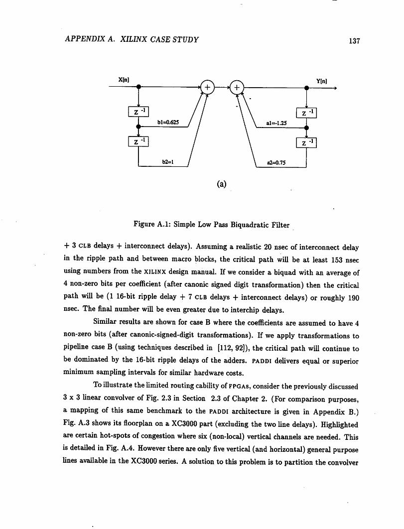
APPENDIX A. XILINX CASE STUDY
X[n]
—<•— 1
z-1 /i
51=0.625 / //
Z"1 /b2=l /
(a)
\ ^
Y[n]
/
al=-1.25
1 r
A z1
\\ J >\
a2=0.75
\ Z'1
\
Figure A.l: Simple Low Pass Biquadratic Filter
137
+ 3 clb delays + interconnect delays). Assuming a realistic 20 nsec of interconnect delayin the ripple path and between macro blocks, the critical path will be at least 153 nsec
using numbers from the XILINX design manual. If we consider a biquad with an average of
4 non-zero bits per coefficient (after canonic signed digit transformation) then the critical
path will be (1 16-bit ripple delay + 7 clb delays + interconnect delays) or roughly 190nsec. The final number will be even greater due to interchip delays.
Similar results are shown for case B where the coefficients are assumed to have 4
non-zero bits (after canonic-signed-digit transformations). If we apply transformations to
pipeline case B (using techniques described in [112, 92]), the critical path will continue to
be dominated by the 16-bit ripple delays of the adders, paddi delivers equal or superiorminimum sampling intervals for similar hardware costs.
Toillustrate the limited routing cability of FPGAs, consider the previously discussed
3x3 linear convolver of Fig. 2.3 in Section 2.3 of Chapter 2. (For comparison purposes,
a mapping of this same benchmark to the paddi architecture is given in Appendix B.)Fig. A.3 shows its floorplan on a XC3000 part (excluding the two line delays). Highlightedare certain hot-spots of congestion where six (non-local) vertical channels are needed. This
is detailed in Fig. A.4. However there are only five vertical (and horizontal) general purposelines available in the XC3000 series. A solution to this problem is to partition the convolver

APPENDIX A. XILINX CASE STUDY 138
X[n]
(b)
Figure A.2: Transformed Biquad
across 3 chips* one per vertical section (Table A.l). paddi again delivers a superiorminimum
sampling interval for similar hardware costs.
When we started our investigations only the XC3000 family was available. The
recently introduced of the xilinx XC4000 series which uses 0.8 and 0.5 fim cmos technol
ogy and which has hooks for faster adders, and a different interconnect architecture will
affect the above comparison. The XC4000 series alleviates some of the the abovementioned
limitations by incorporating special architectural hooks for faster addition (20nsec per 16
bits in 8 clbs). Per column there are now 8 single length lines, 2 double length lines, and
6 long lines but the switching matrices are less powerful than in the XC3000. Without fur
ther detailed study one cannot make definite conclusions about the new family's ability to
support high speed dsp algorithms. We also note that the XC3000 family was implemented
in 1.2 ^m CMOS as is our prototype chip whereas the XC4000 is implemented in 0.8 f.tm
CMOS. The XC4005 (14 x 14 clbs) is being sampled with the XC4010 (20 x 20) planned
before going to 0.5 ^m technology. The difference in implementation technology will, com
plicate the task of comparison, vsps [127] and commercial DSPs are other programmable
alternatives. In future comparisons, one must take into account the technology and archi
tectural differences and also the on chip hardware multiplexing support of paddi which is
not present in conventional fpgas. However, because of the features described above i.e.

APPENDIX A. XILINX CASE STUDY
16-bttlinedelayed inputs (use3 verticallonglinn)
>16 >16 >16ROWS
Rl
R2
R3
R4
R5
R6
R7
R8
R9 Ct!]
RIO
rii ED
R12
R13
R14
R1S
R16
ED
\~r*\
EpEg
S.
fi?
registeredoutput
saf
l±2!
Figure A.3: Convolver on XC3090 with Routing Congestion
R4
R5
R6
bitl
register
adder
register
bit2
register
adder
register
*
Figure A.4: Insufficient Routing Resources for the Convolver
139
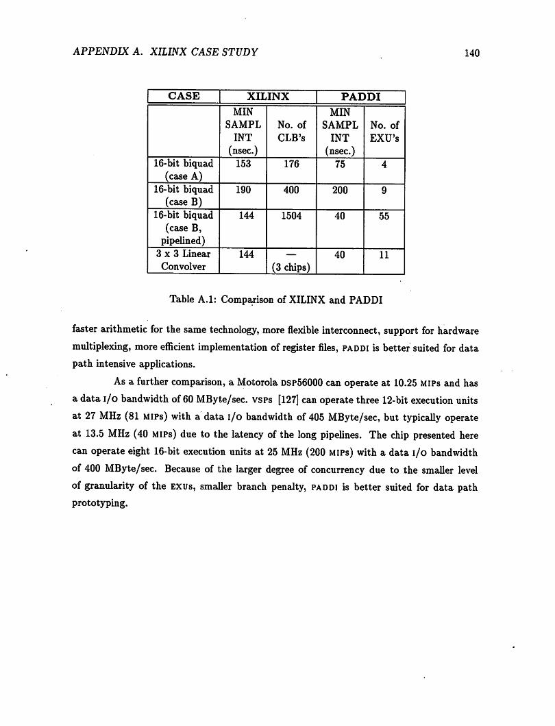
APPENDIX A. XILINX CASE STUDY
CASE XILINX PADDI
MIN
SAMPL
INT
(nsec.)
No. of
CLB's
MIN
SAMPL
INT
(nsec.)
No. of
EXU's
16-bit biquad(case A)
153 176 75 4
16-bit biquad(case B)
190 400 200 9
16-bit biquad(case B,
pipelined)
144 1504 40 55
3x3 Linear
Convolver
144
(3 chips)40 11
Table A.l: Comparison of XILINX and PADDI
140
faster arithmetic for the same technology, more flexible interconnect, support for hardware
multiplexing, more efficient implementation of register files, PADDI is better suited for data
path intensive applications.
As a further comparison, a Motorola DSP56000 can operate at 10.25 mips and has
a data i/o bandwidth of 60 MByte/sec. vsps [127] can operate three 12-bit execution units
at 27 MHz (81 mips) with a data i/o bandwidth of 405 MByte/sec, but typically operate
at 13.5 MHz (40 mips) due to the latency of the long pipelines. The chip presented here
can operate eight 16-bit execution units at 25 MHz (200 mips) with a data i/o bandwidth
of 400 MByte/sec. Because of the larger degree of concurrency due to the smaller level
of granularity of the EXUs, smaller branch penalty, PADDI is better suited for data pathprototyping.

Appendix B
Mapping an Example to PADDI
Table B.l shows several benchmarks which were manually mapped onto the paddiarchitecture.
Below, we show how one of these examples maps to the architecture. It is the 3 x
3 linear convolver of Fig. 2.3 of Section 2.3. The coefficients, are powers-of-two and so the
multiplications can be implemented as shifts and adds. This convolver is used in low level
image processing [103] to implement various filtering operations.
After retiming [68], the signal flow diagram of Fig. B.l results. Fig. B.2 and
Fig. B.3 show how this can be mapped to two chips (excluding the line delays). (Note
also that the pads of each chip are pipelined). In this example the SFG is mapped directly
to hardware and there is no hardware multiplexing of operations on the exus. The EXUs
receive a single static global instruction, and the instructions pins can be hard-wired to a
constant value.
141
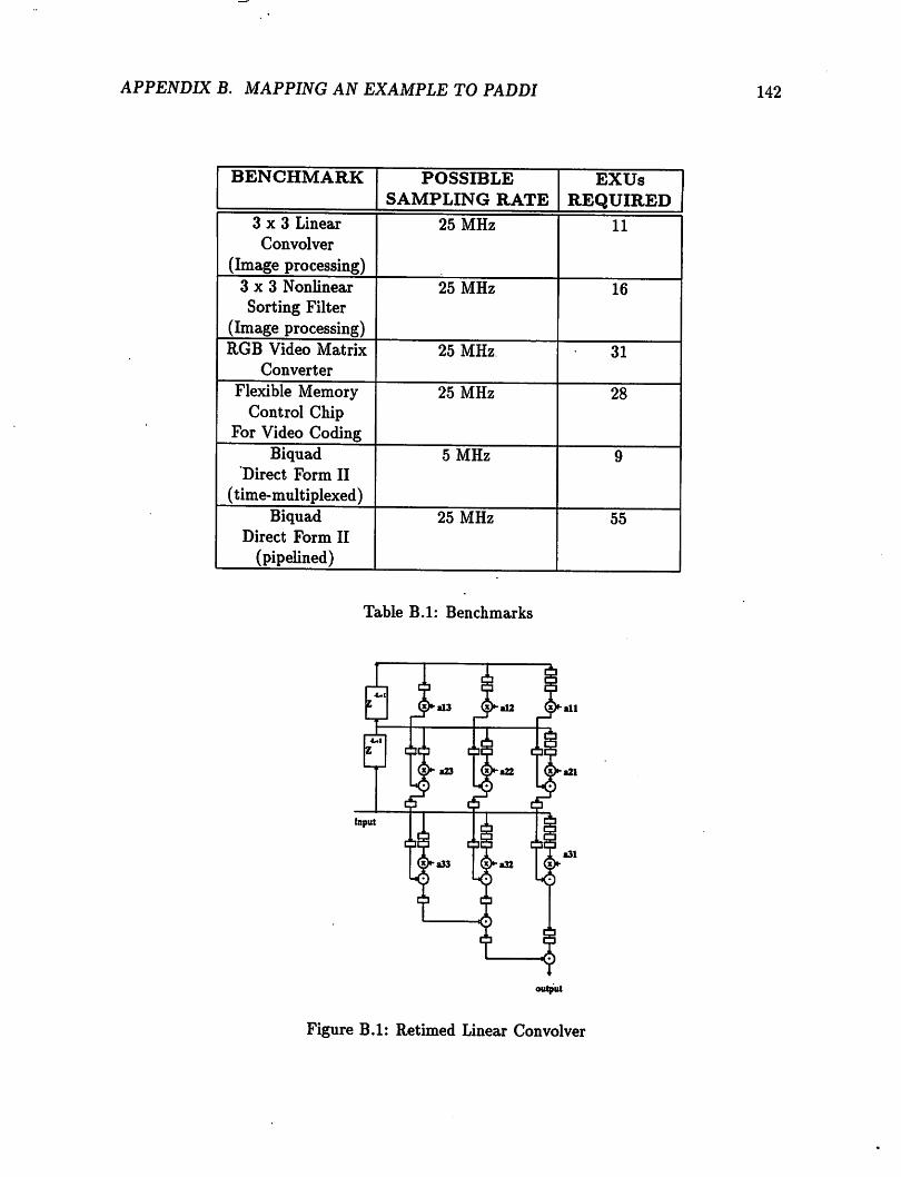
APPENDIX B. MAPPING AN EXAMPLE TO PADDI
BENCHMARK POSSIBLE
SAMPLING RATE
EXUs ,
REQUIRED
3x3 Linear
Convolver
(Image processing)
25 MHz 11
3x3 Nonlinear
Sorting Filter(Image processing)
25 MHz 16
RGB Video Matrix
Converter
25 MHz 31
Flexible MemoryControl Chip
For Video Coding
25 MHz 28
BiquadDirect Form II
(time-multiplexed)
5 MHz 9
BiquadDirect Form II
(pipelined)
25 MHz 55
Table B.l: Benchmarks
output
Figure B.l: Retimed Linear Convolver
142
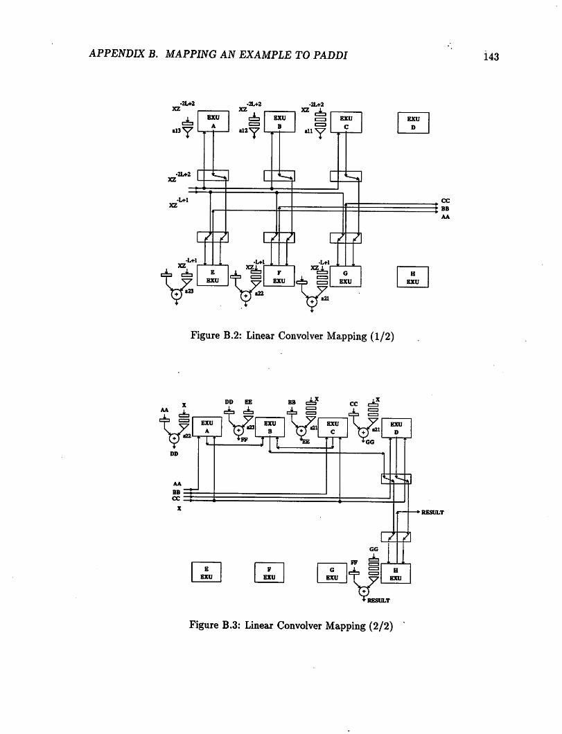
APPENDIX B. MAPPING AN EXAMPLE TO PADDI
-21*2xz
•13^7 \-j
-2L+2XZ
•L+lXZ
-L+lXZ
•23
BXU
A
7
E
BXU
-2L+2XZ
•12^
-L+lXZ^
•22
BXU
B
7 7
F
BXU
-2L+2XZ ^
all Y
-L+l
•21
BXU
C
7
G
BXU
BXU
D
H
BXU
Figure B.2: Linear Convolver Mapping (1/2)
AA±
♦ ) ^Vr
DD
AA
BXU
A
DD BB
•23
FF
BXU
B
BB ci?
«21EXU
C
CC ^
•21
GG
EXU
D
;* BBAA
CC ^
X•* RESULT
B
BXU
F
BXU
G
BXU
FF
cz aGG
H
EXU
RESULT
Figure B.3: Linear Convolver Mapping (2/2)
143

Appendix C
Programmer's Guide
C.l Introduction
This Appendix provides an overview of the assembly language supported by the
high level compiler.
The operations of the machine determined by two types of information: initial
configuration settings, and run time instructions. After configuration, each EXU accepts
run-time instructions which specify its operation, and the routing of the data. In model of
execution that was adopted, each EXU always issues it's output to the crossbar switch, as
a consequence, there is no specification of any particular destination be it internal register,
other EXU or i/o port. This "receiver controlled" model was described in Section 7.2.1.
C.l.l Dynamic Instructions
We will begin by describing the format of the dynamic or run-time instructions.
Each exu's operation in a given cycle is specified by a fifty-three bit instruction
word. The instruction format is shown in Fig. C.l. Two fields specify read and write
addresses for the A and B register files. The function field specifies the EXU function. The
switch fields are used to specify the sources of data for each of the register files. Sources
can be the outputs of any EXU or any of four input busses. The flags field sets the interrupt
enable flags for interrupt vectors IVONE and IVTWO respectively.
Each instruction executes in one cycle. We will now describe the separate fields
which are contained in an instruction.
144

APPENDIX C. PROGRAMMER'S GUIDE
REGISTER
A REGISTER
SPECIFIERS
FILESB REGISTER
SPECIFIERS
FUNCTIONFUNCTION
SPECIFIERS
OUTPUT BUS
ENABLES
SWITCHA REGISTER
SOURCE
B REGISTER
SOURCE
FUGSINTERRUPT
ENABLES
145
6 (bits)
6
11
2
13
13
2
Figure C.l: Instruction Format
Registers
Each EXU has two dual-ported register files (See Section 5.5.1) designated A and
B. Each register file contains six registers Al .. A6 and Bl .. B6. The registers A6 and
B6 are special i.e. they can be initialized to contain an arbitrary value.
Each EXU instruction contains specifiers for both read source register and write
destination register for each register file. Source and destination register specifiers can be
identical. The source register will be read at the beginning of the cycle, and the destination
register will be written at the end of the cycle.
Functions
A summary of the various EXU functions is shown in Table C.l. Accumulation in
a given exu is achieved by specifying register for reading and writing i.e. the accumulator
and the source unit for the write register to be "this-EXU"
Output Bus Enables
There are four 16b output buses OIL, OlH, 02L, 02H that communicate with
the external world. The routing of data to these buses is controlled by the output bus

APPENDIX C. PROGRAMMER'S GUIDE
Description Op-code Operand
Load = src
Addition + srcl, src2
Subtraction - srcl, src2
Maximum max srcl, src2
Minimum min srcl, src2Arithmetic
Right Shift> amount
Insert outputpipeline register
oreg
No operation nop
146
Table C.l: Summary of Arithmetic Instructions
enaMe fields. EXUs A, C, E, F can write to buses OIL and 02L while EXUs B, D, G, H
can write to buses OlH and 02H. In 32bmode, e.g. where EXUs A and B might be linked
and routed to output bus 1, the output from A would form the lower half of the output
word, and the output from B would form the upper half.
The assembler automatically checks for and flags any bus conflicts which mightoccur due to an error in the code.
A and B Register Sources
The A and B register sources fields control the switch settings of the crossbar net
work to determine the routing ofdata. These fields are implicitly specified by the assembly
code by the the sources (exus and/or input buses) for each register, and automaticallygenerated by the assembler.
There are four 16b input buses, I1L, I1H, I2L, and I2H respectively. There are
no restrictions on which input bus might be routed to any EXU.
Interrupt Enables
An EXU canbe interrupted from the normal control flow ifeitherofits twointerrupt
enable flags are set as described in Section 5.5.3.

APPENDIX C. PROGRAMMER'S GUIDE
Description Op-code Operand
Specifying constants = value
Normal registerfile mode (A)
normal-a
Normal registerfile mode (B)
normal-b
Delay registerfile mode (A)
delay-a
Delay registerfile mode (B)
delay_b
Link exus link
Unlink exus unlink
Unsigned arithmetic unsignedTwo's complement
arithmetic
signed
147
Table C.2: Summary of Configuration Specifiers
C.l.2 Configuration Specifiers
We will now describe the various fields which control the initial configuration and of
the machine. Apart from the constant register which may be overwritten, the configuration
remains static until the next re-boot. Table C.2 lists the various configuration specifiers.
C.1.3 Putting it all Together
The following program does not perform any meaningful operation. The listing is
presented to illustrate the syntax of the assembly language and a will be useful reference
to the assembly language programmer. It contains examples of all the main assembly
instructions with appropriate comments. (The reader may refer to Section 6.7.2 for some
real program listings)./* global defaults section
* these can be overridden at the specific EXU defaults
* section
*/
defaults {
A6=0, B6=0, /* initial values for constant regs */
bfsw=llllllllb, /* buffer switch value (note the binary
constant) */
normal-a, /* normal mode for reg file A */

APPENDIX C. PROGRAMMER'S GUIDE 148
normalJb, /* normal mode for reg file B */
ienl=0, ien2=0, /* turn off interrupts */
unlink, /* don't link EXUs */
oreg=OxABCD, /* pipeline reg value (note the hex
constant) */
signed /* signed mode */
}
/* symbol name to EXU letter maps */map {
(exu-a=Xa), (exu-b=Xb), (exu-c=Xc), (exujd=Xd),(exu-e=Xe), (exu-f=Xf), (extug=Xg), (exuii=Xh)
>/* for delay line mode, all incoming values*must* go to
* reg num 5
•/#define DELAY-REG-A A5
#define DELAY-REG.B B5
exu-a
link, /* link mode */
delay-a /* delay line mode for register A */
/* if you don't specify an instruction number,
* the instruction number defaults to the next
* available instruction 'slot' (in this case
* instruction zero)
•/
{
DELAY-REG-A=ill, oreg (Al+Bl), ol;
/* read in from external world input
bus 1L, latch the output, and
output it on external world output
bus 1 (either 1H or 1L, whatever is
valid) */
exu-b
link, /* link mode */
delay-a /* delay line mode for register A */
{
DELAY-REG-A=ilh, oreg (Al+Bl), ol;
}

APPENDIX C. PROGRAMMER'S GUIDE 149
exujc unsigned,a6=1234 /* decimal value 1234(base 10) */
{1: nop;
0: a5=exu-a, b5=exu_b, (max(a5, (b5>l))), o2;
7: a5=ill, b5=i2l, (min(a5,b5>7)), o2;
}
exu-d a6=l, b6=l, flagl=ill, ivecl=0 { /* usage of flags*/
0: a5= ill, (a5), ol, o2;
1: a5= ill, (a5+b6), ienl, ol, o2;
}
Appendix D
Configuration With External
Memory
The paddi chip caninterface directly to external memorywith minimal glue logic.
Commercial eproms (such as the xilinx XC1736 and XC1764) which have internally.re-
settable counters, are available. The paddi chip can interface directly to these with no gluelogic whatsoever.
Internally generated phim and PHIS non-overlapping, two-phase clocksare provided
for external synchronization. After an initializing START signal (e.g. power on reset) is
received by the paddi chip, the low during configuration (ldc) signal will toggle, the chip
enable (ce) will go low, and scan signal will go high (Fig. D.l). The scan signal will
remain high for the duration of a complete line scan. It will then go low to allow writing
of the on board srams and then return high. This will repeat until all 8 nanostore entries
are fully configured. After configuration is completed, the scan signal will be set low andldc and ce will be set high.
The actual circuits used during chip paddi testing are shown in Fig. D.2 and are
presented as a convenience for future users.
150

APPENDIX D. CONFIGURATION WITH EXTERNAL MEMORY
PHM
PHS
JLJUUOfUlJULMJULRMMJ^
JUUUlMlJliyiJlMJLnXfU^
START
LDC
CE
SCAN mmjn
Figure D.l: Configuration Timing Diagram
r>
PHM
CE
/LOAD
A
B
C COUNTER
D 169'
/HOT /ENP
SCANC
EPROM
4 tttdreu
SCAND4
PADDI
Figure D.2: Interfacing to External Memory
r
r
151

Appendix E
Pin List
E.l Pad Types
The pin grid array (pga) pin assignments are shown in Fig. E.l. The package
is a 208 pin pga manufactured by the Kyocera Corporation. The type field refers to the
type of pad that is used for a particular pin. There are two basic types, non-registered and
registered. Tables E.2 and E.3 show the paddi pin list. The correspondence between pad
types and pin types is given in Table E.l.
Pad Name Description Pin Type
padBin non-registered input pad Bin
padininv non-registered inverting input pad ininv
padbo non-registered output pad bo
padin registered input pad in
pado tri-stated registered o/p pad out
Table E.l: Pad Types
152

APPENDIX E. PIN LIST
E.2 PGA Pinout
208 PGA
17 ®®®®®®®®®®®®®®®®®16 ®®®®®®®®®®®®®®®®®IS ®®®®®®®®®®®®®®®®®14
13
®®®®®®®®®®®®®®®®®_ _ „_ 2J i» iu i» us iw im ui u* in i»® ® ® ®im ,«© © © ©
12 © © © ©*
© © © ©•
M IM in© © © ©
171© © © ©11•IM m
10 ^3 ^9 ^9 ^9" air 177® © © ©
9 © © © ©n BOTTOMVBW in© © © ©
8 © © © ©» i in© © © ©
7 © © ©. ©a iat
m© © © ©
6 ^ff ^p © ©0 „ »**»« 1 IN© © © ©
5
4
® ® ® ©» ® »® ® ® ®© © ®© e©©©©©©©©©©®®
3 ®®®®®®e®®®®®®®®®®2 ®®®®®®®®®®®®®®®®®1 ©©©©©©©©©©©©©©©©©
A B C D E FGHJ KLMNPRST
BOTTOM VIEW
13 Low inductance/resistance pins are thoseclosest to the die edge.
E Pins 11,63,115,167 are connected to substrate.
• Diemounted ontopside.
Figure E.l: PADDI PGA Pin Assignments
153
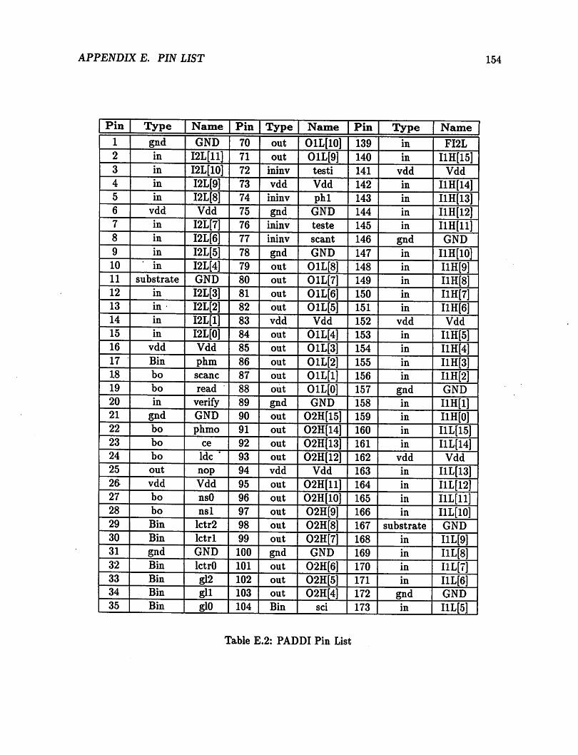
APPENDIX E. PIN LIST
Pin Type Name Pin Type Name Pin Type Name
1 gnd GND 70 out OlL[10] 139 in FI2L
2 in I2L[11] 71 out 01L[9] 140 in I1H[15]3 in I2L[10] 72 ininv testi 141 vdd Vdd
4 in I2L[9] 73 vdd Vdd 142 in I1H[14]5 in I2L[8] 74 ininv phi 143 in I1H[13]6 vdd Vdd 75 gnd GND 144 in I1H[12]7 in I2L[7] 76 ininv teste 145 in I1H[11]8 in I2L[6] 77 ininv scant 146 gnd GND
9 in I2L[5] 78 gnd GND 147 in I1H[10]10 in I2L[4] 79 out 01L[8] 148 in I1H[9]11 substrate GND 80 out 01L[7] 149 in I1H[8]12 in I2L[3] 81 out 01L[6] 150 in I1H[7]13 in I2L[2] 82 out 01L[5] 151 in I1H[6]14 in I2L[1] 83 vdd Vdd 152 vdd Vdd
15 in I2L[0] 84 out 01L[4] 153 in I1H[5]16 vdd Vdd 85 out 01L[3] 154 in I1H[4]17 Bin phm 86 out 01L[2] 155 in I1H[3]18 bo scanc 87 out 01L[1] 156 in I1H[2]19 bo read 88 out OlL[0] 157 gnd GND20 in verify 89 gnd GND 158 in I1H[1]21 gnd GND 90 out 02H[15] 159 in I1H[0]22 bo phmo 91 out 02H[14] 160 in I1L[15]23 bo ce 92 out 02H[13] 161 in I1L[14]24 bo ldc ' 93 out 02H[12] 162 vdd Vdd
25 out nop 94 vdd Vdd 163 in I1L[13]25 vdd Vdd 95 out 02H[11] 164 in I1L[12]27 bo nsO 96 out O2H[10] 165 in I1L[11]28 bo nsl 97 out 02H[9] 166 in I1L[10]29 Bin lctr2 98 out 02H[8] 167 substrate GND
30 Bin lctrl 99 out 02H[7] 168 in I1L[9]31 gnd GND 100 gnd GND 169 in I1L[8]32 Bin IctrO 101 out 02H[6] 170 in I1L[7]33 Bin gl2 102 out 02H[5] 171 in I1L[6]34 Bin gu 103 out 02H[4] 172 gnd GND35 Bin gio 104 Bin sci 173 in I1L[5]
Table E.2: PADDI Pin List
154
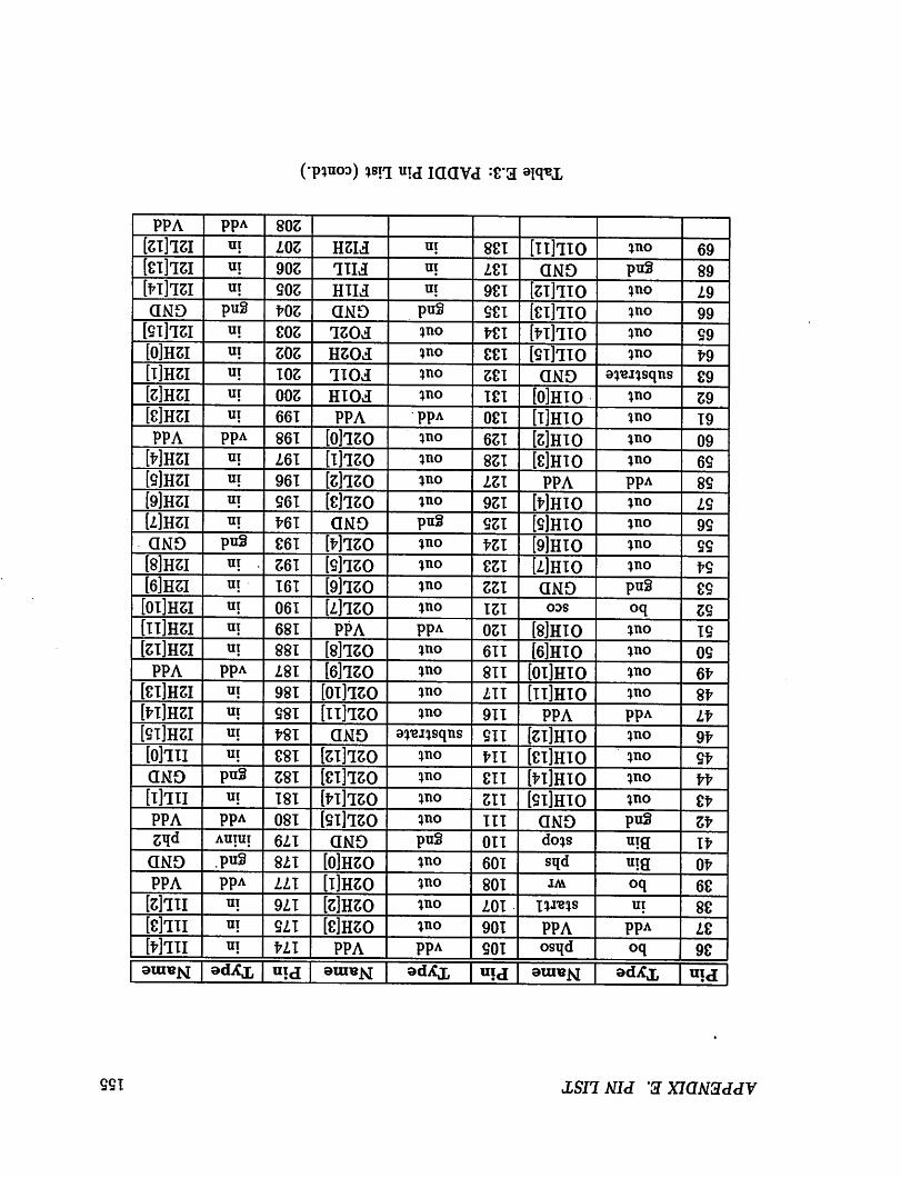
APPENDIXE.PINLIST
PinTypeNamePinTypeNamePinTypeName
36bophso105vddVdd174inI1L[4]37vddVdd106out02H[3]175inI1L[3]38instart1107out02H[2]176inI1L[2]39bowr108out02H[1]177vddVdd
40Binphs109outO2H[0]178gndGND41Binstop110gndGND179ininvph242gndGND111out02L[15]180vddVdd
43out01H[15]112out02L[14]181inI1L[1]44out01H[14]113out02L[13]182gndGND45out01H[13]114out02L[12]183inI1L[0]46out01H[12]115substrateGND184inI2H[15]47vddVdd116out02L[11]185inI2H[14]48out01H[11]117outO2L[10]186inI2H[13]49outOlH[10]118out02L[9]187vddVdd
50out01H[9]119out02L[8]188inI2H[12]51out01H[8]120vddVdd189inI2H[11]52boSCO121out02L[7]190inI2H[10]53gndGND122out02L[6]191inI2H[9]54out01H[7]123out02L[5]192inI2H[8]55out01H[6]124out02L[4]193gndGND56out01H[5]125gndGND194inI2H[7]57out01H[4]126out02L[3]195inI2H[6]58vddVdd127out02L[2]196inI2H[5]59out01H[3]128out02L[1]197inI2H[4]60out01H[2]129outO2L[0]198vddVdd
61out01H[1]130vdd.Vdd199inI2H[3]62outOlH[0]131outF01H200inI2H[2]63substrateGND132outFOIL201inI2H[1]64out01L[15]133outF02H202inI2H[0]65out01L[14]134outF02L203inI2L[15]66out01L[13]135gndGND204gndGND
67out01L[12]136inFI1H205inI2L[14]68gndGND137inFI1L206inI2L[13]69out01L[11]138inFI2H207inI2L[12]
208vddVdd
TableE.3:PADDIPinList(contd.)
155

Appendix F
Assembler Manual Page
P.l Introduction
PAS(l) USER COMMANDS PAS(l)NAME
pas - PADDI assembler
SYNOPSIS
pas [-ENPWsv] [-T type ] [-e errors ] [-i instruction ][-o objfile ] filename
DESCRIPTION
Pas translates the PADDI assembly language source file,
filename, into an object file, either the base of filename
followed by an aproposextension (the object file type name)or the specified objfile.
OPTIONS
Pas supports the following command-line options:
-E Do not display any error messages.
-N Do not display any informational messages(or"notes").
-P Do not apply the standard UNIX C language preprocessor,
cpp, to the input file. If this option is specified,
then the standard C language comments will
cause problems for the parser.
-W Do not display any warning messages.
-s Do not perform any semantic checking.
-v Show the current version information. -T type The
argument type specifies the object file type. See the
below section OBJECT FILE TYPES for more details. This
option was originally "-0" and later M-M."
-e errors
The argument errors specifies the maximum number of
156

APPENDIX F. ASSEMBLER MANUAL PAGE 157
errors allowed before pas terminates (the default is
ten).
-i instruction
The argument instruction specifies a specific instruc
tion number to assemble for the scandas and scantest
object file types (the default is "-1" or all
instructions).
-o objfile
The argument objfile specifies the output object file.
OBJECT FILE TYPES
Pas supports several different object file types:
eprom
This object file type is a straight ASCII file of bytes
in hexadecimal form, suitable for loading into an EPROM
programmer.
irsim
This object file type provides eight object files (one
for each instruction within the nanostore) which (after
manual massaging) is suitable for loading into the
irsim switch-level simulator.
obj This object file type is a "portable" object file
suitable for loading the PADDI simulator psim. This is
the default object file type.
scandas
This object file type provides either eight object
files (one for eachinstruction within the nanostore)or a single object file (the instruction specified by
the "-i" option) and is suitable for use with das.
scantest
This object file type provides either eight object
files (one for each instruction within the nanostore)or a single object file (the instruction specified by
the "-i" option) and is suitable for use with the
scantest program.) if mixed-case keywords are a problem.
AUTHOR
Eric Ng
University of California, Berkeley
Internet: [email protected]
UUCP: ...!ucbvax!zabriskie!erc
Sun Release.4.1 Last change: February 1992

Appendix G
Annotated grammar
G.l Annotated Assembler Grammar
The grammar presented below is the actual yacc parser-generator grammar used
by the paddi assembler (with a few modifications for increased clarity). There are sev
eral undefined terminal symbols which are clarified within the annotations below: boolean-
state, flag-output-bus-id, integer-constant, input-bus-id, interrupt-id, output-bus-id, register-
number, and string-label. Text expressed in the typewriter font are terminal symbols given
literally.
For convenience, pas applies cpp (the standard unix C language preprocessor)
to input files (unless instructed not to do so). Hence standard C language comments are
supported (7* ... */'), as are the usual preprocessor directives ('#def ine' and '#include').
•program.'.
execution-unit-defaults execution-unit-mappings execution-unit-program-list
A paddi assembler program consists of three parts: the execution unit default settings,
the execution unit mapping table, and the program list.
execution-unit-defaults'.
nothing
defaults { execution-unit-config-list }
All settings except for flag and flagout can be assigned default values here.
execution-unit-mappings:
map { execution-unit-mapping-list }
execution-unit-mapping-list:
execution-unit-id-mapping
execution-unit-id-mapping , execution-unit-mapping-list
158
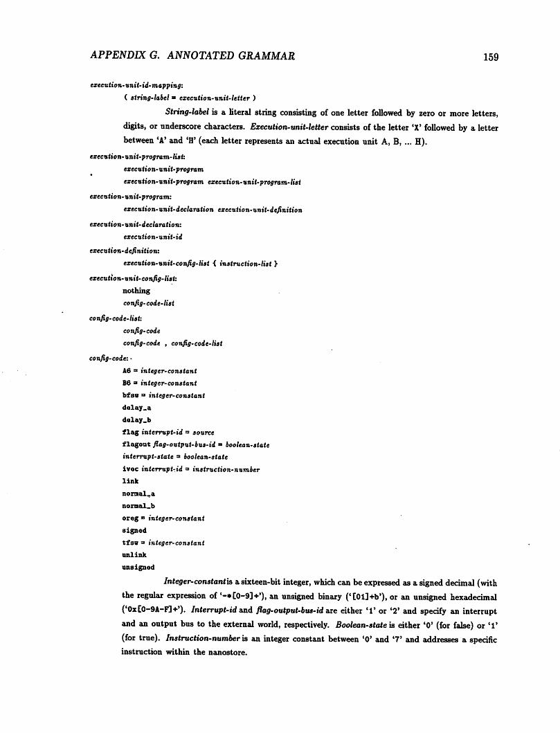
APPENDIX G. ANNOTATED GRAMMAR 159
execution-unit- id- mapping:
( string-label = execution-unit-letter )
String-label is a literal string consisting of one letter followed by zero or more letters,
digits, or underscore characters. Execution-unit-letter consists of the letter 'X' followed by a letterbetween 'A' and 'H' (each letter represents an actual execution unit A, B, ... H).
execution-unit-program-list:
execution-unit-program
execution-unit-program execution-unit-program-list
execution-unit-program:
execution-unit-declaration execution-unit-definition
execution-unit-declaration:
execution-unit-id
execution-definition:
execution-unit-config-list { instruction-list }
execution-antt-config- list:
nothing
config-code-list
config-code-list:
config-code
config-code , config-code-list
config-code: •
A6 » integer-constant
B6 = integer-constant
bfsw = integer-constant
delay.a
delay.b
flag interrupt-id = source
flagout flag-output-bus-id " boolean-state
interrupt-state = boolean-state
ivec interrupt-id = instruction-number
link
nortnal.a
normal.b
oreg ° integer-constant
signed
tfsw = integer-constant
unlink
unsigned
Integer-constantis asixteen-bit integer, which can beexpressed asa signed decimal (withthe regular expression of '-*[0-9]+'), an unsigned binary ('[Oll+b'), or an unsigned hexadecimal('0x[0-9A-F]+'). Interrupt-id and flag-output-bus-id are either '1' or '2' and specify an interruptand an output bus to the external world, respectively. Boolean-state is either c0' (for false) or *1'(for true). Instruction-number is an integer constant between '0' and '7* and addresses a specificinstruction within the nanostore.

APPENDDCG. ANNOTATED GRAMMAR 160
instruction-list:
instruction-prefix instruction
instruction-prefix instruction instruction-list
instruction-prefix:
nothing
instruction-number :
If no instruction-prefix is given, the current instruction is placed at the first empty
location within the nanostore, starting at zero.
instruction:
' bit-string » ;
code-list ',
nop ;
Bit-string is fifty-three bits long and allows for the explicit specification of an instruc
tion within the nanostore. A nop is results in an instruction consisting entirely of zeroes; a nop
with destination-register, interrupt-state, and output-bus-idcodes can be expressed by omitting theexpression code.
code-list:
code
code , code-list
code:
( expression )
oreg ( expression )
destination-register = source
interrupt-state
0 output-bus-id
Interrupt-state and output-bus-idcodes reverse their respective default states (i.e., spec
ifying an interrupt-state code for a previously enabled interrupt will disable it for that particularinstruction).
source:
execution-unit-id
1 input-bus-id
Input-bus-id specifies a particular input bus from the external world (with a regularexpression of *[12] [HL] ')•
expression:
source-register
source-register operator source-register
function ( source-register , source-register )
operator:
+
function:
max
min

APPENDIX G. ANNOTATED GRAMMAR 161
execution-unit-id:
string-label
destination-register:
A register-number
B register-number
Register-numberis an integer between '1' and '6' and addresses a specific register withinthe given register file.
source-register.
A register-number
B register-number
B register-number » integer-constant
( B register-number » integer-constant )
interrupt-state:
ien interrupt-id
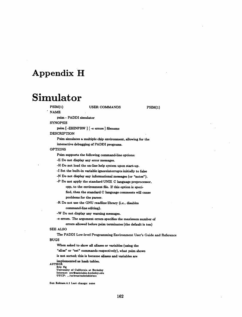
Appendix H
SimulatorPSIM(l) USER COMMANDS PSIM(l)
' NAME
psim - PADDI simulator
SYNOPSIS
psim [-EHINPRW ] [-e errors ] filename
DESCRIPTION
Psim simulates a multiple chip environment, allowing for the
interactive debugging of PADDI programs.
OPTIONS
Psim supports the following command-line options:
-E Do not display any error messages.
-H Do not load the on-line help system upon start-up.
-I Set the built-in variable ignoreinterrupts initially to false
-N Do not display any informational messages(or "notes").
-P Do not apply the standard UNIX C language preprocessor,
cpp, to the environment file. If this option is speci
fied, then the standard C language comments will cause
problems for the parser.
-R Do not use the GNU readline library (i.e., disables
command-line editing).
-W Do not display any warning messages.
-e errors. The argument errors specifies the maximum number of
errors allowed before psim terminates (the default is ten)
SEE ALSO
The PADDI Low-level Programming Environment User's Guide and Reference
BUGS
When asked to show all aliases or variables (using the
"alias" or "set" commands respectively), what psim shows
is not sorted; this is because aliases and variables are
implemented as hash tables.AUTHOR
Eric NgUniversity of California at BerkeleyInternet: ercOsabriskie.berkeley.eduUUCP: ...!ucbvax!zabriskie!erc
Sun Release.4.1 Last change: none
162

APPENDIX H. SIMULATOR
plitvice:biquad 55% pas biquad. 30 errors, 0 warnings, and 0 messages total7k bytes allocatedplitvice:biquad 56% p3im biquad. epsim 0.9 (compiled Apr 18 1992)Reading environment configuration file...Constructing simulation environment. ..Loading object file 'biquad.obj' for chip 'chip_one'Loading on-line help system.(psim) breakpoint chip_one + 3breakpoint set at 'chip_one', exu A, instruction 3breakpoint set at 'chip_one', exu B, instruction 3breakpoint set at 'chip_one', exu C, instruction 3breakpoint set at 'chip~one\ exu D, instruction 3breakpoint set at 'chip_one\ exu E, instruction 3breakpoint 3et at 'chip_one', exu F, instruction 3breakpoint set at 'chip_one', exu G, instruction 3(p3im) run . "breakpoint at 'chip_one', exu A, instruction 3(psim) dumpexu chip_one a pcchip 'chip_one', exu A (file 'biquad.obj')
A1=0 A2=0 A3=0 A4=0 A5=0 A6=-2 Bl-0 B2=-2 B3=2 B4=0 BS=0 B6=0oreg-0 delA-0 delB-0 signed-1 link-0 ftriout-00 intvecl-0 intvec2»0fswl=0000000000b fsv2=0000000000000000b intsrcl=null intsrc2=nullresult-2 flag-1 lastpc-2 pc-3 intl-0 int2-0
3: dregA=6 sregA=3 dregB=6 sregB=3 rs=0 add=l raax=0 h3el=0 hin=0 gsel=0latch-0 asel-0 bsel-0 ienl-0 ien2-0 triout-10svl=0000001100b sv2=0000000000001100b 3rcA=XB 3rcB=XB
(psim) dumpexu chip_one b nonechip 'chip one', exu B (file 'biquad.obj')
Al-0 A2-0 A3-0 A4-0 A5-0 A6-0 Bl-0 B2-0 B3-0 B4-0 BS-0 B6-0oreg=0 delA=0 delB=0 siqned=l link=0 ftriout=00 intvecl=0 intvec2=0fswl=0000000000b fsw2-0u00000000000000b intsrcl-null intsrc2-nullresult=0 flag=l lastpc=2 pc=3 intl=0 int2=0
(psim) step(psim) dumpexu chip_one a pcchip 'chip_one', exu A (file 'biquad.obj')
A1=0 A2=0 A3=0 A4=0 A5=0 A6=0 Bl=0 B2=-2 B3=2 B4=0 B5=0 B6=0oreg-0 delA-0 delB-0 signed-1 link-0 ftriout-00 intvecl-0 intvec2-0fswl=0000000000b fsw2=0000000000000000b intsrcl=null intsrc2=nullresult-2 flag-0 lastpc-3 pc-1 intl-0 int2-0
1: dregA=2 sregA=6 dregB=2 sregB=6 rs=2 add=0 max=0 hsel=0 hin=0 gsel=0latch-0 asel-0 bsel-1 ienl-0 ien2»0 triout-00swl=0000000100b sv2=0000000000000100b srcA=XB srcB=this_exu
(psim) I
Figure H.l: Typical Psim Session
163

Bibliography
[1] "IEEE Micro: Special Issue on Digital Signal Processors", Dec. 1986.
[2] "IEEE Micro: Special Issue on Digital Signal Processors", Dec. 1988.
[3] Advanced Micro Devices Inc.. Array Processing and Digital Signal Processing Handbook, 1986.
[4] M. Ahrens, A. EL Gammal, D. Gailbraith, J. Greene, S. Kaptanoglu, K.R. Dharmara-
jan, L. Hutchings, S. Ku, P. McGibney, K. Shaw, N. Stiawalt, T. Whitney, T. Wong,
W. Wong, and B. Wu. "An FPGA Family Optimized for High Densities and Reduced
Routing Delay". In Proc. CICC'90: 1990 Custom Integrated Circuits Conference,
pages 31.5.1-4, May 1990.
[5] Altera Corp. User-Configurable Logic - Data Handbook, July 1988.
[6] D. Amrany, S. Gadot, and M. Dimyan. "A Programmable DSP Engine for High-
Rate Modems". In Proceedings International Solid State Circuit Conference, pages
222-223, Feb. 1992.
[7] W. Andrews. "Distinctions Blur Between DSP Solutions". Computer Design, pages86-99, May. 1989.
[8] P.J. Berkhout and L.D.J. Eggermont. Digital Audio Systems. IEEE ASSP Magazine,pages 45-67, Oct. 1985.
[9] P. Bertin, D. Roncin, and J. Vuillemin. "Programmable Active Memories", presentedat the 1992 ACMInternational Workshop on Field- Programmable Gate Arrays, pages57-59, Feb. 1992.
164

BIBLIOGRAPHY 165
[10] R. Bisiani. "System Implementation Strategies". In Speech And Natural LanguageWorkshop, June 1990.
[11] W. E. Blanz, D. Petkovic, and J. L. C. Sanz. "Algorithms and Architectures for
Machine Vision (chapter)". In C. H. Chen, editor, Handbook of Signal Processing.Marcell Decker, 1988.
[12] R.K. Brayton. "SRC Center Of ExceUence In CAD/IC". 1990 Research PlanningReport, pages 1-45, 1990.
[13] R.K. Brayton, R. Rudell, A. Sangiovanni-Vincentelli, and A.Wang. "MIS: A MultipleLevel Logic Optimization System". IEEE Transactions on Computer Aided Design,CAD-6(6):1062-1081, Nov. 1987.
[14] R.W. Brodersen, A. Chandrakasan, and S. Sheng. "Technologies for Personal Communications". VLSI Symposium, 1991.
[15] R.W. Brodersen and J. Rabaey. "Evolution ofMicrosystem Design". In ESSCIRC'89:Proceedings ofthe 15th European Solid State Circuits Conference, pages 208-217, Sept.1989.
[16] R. Budzinski, J. Linn, and S. Thatte. "A Restructurable Integrated Circuit for Implementing Programmable Digital Systems". Computer, pages 11-21, Mar. 1982.
[17] D. Bursky. "Programmable Sequencer Hits 125-MHz Clock Speed". Electronic Design, pages 43-46, September 1989.
[18] D. Bursky. "DSP Expands Role As Cost Drops And Speed Increases". ElectronicDesign, pages 53-81, Oct 1991.
[19] D. Bursky. "Parallel Processing DSP Chip Delivers Top Speed". Electronic Design,pages 43-50, Oct 1991.
[20] F. Catthoor. "Microcoded Processor Architectures and Synthesis Methodologies forReal-Time Signal Processing". In E.F. Depreterre and A-J. van der Veens, editors,
Algorithms and Parallel VLSI Architectures, pages 403-429. Elsvier Science, 1991.Vol. A.

BIBLIOGRAPHY 166
[21] P.K. Chan, M. Schlag, and M. Martin. "BORG: A Reconfigurable Prototyping Board
Using FPGAs". presented at the 1992 ACM International Workshop on Field- Pro
grammable Gate Arrays, pages 47-51, Feb. 1992.
[22] D. C. Chen, R. Yu, R. W. Brodersen, and J. Rabaey. "A VLSI Grammar Process
ing Subsystem for a Real Time Large Vocabulary Continuous-Speech Recognition
System". In Proc. CICC'90: 1990 Custom Integrated Circuits Conference, pages
13.3.1-5, May 1990.
[23] D.C. Chen, L.M. Guerra, E.H. Ng, , M. Potkonjak, D.P. Schultz, and J.M. Rabaey.
"An Integrated System for Rapid Prototyping of High Algorithmic Specific Data
Paths", to be presented at the International Conference on Application-Specific Array
Processors, Aug. 1992.
[24] D.C. Chen, L.M. Guerra, E.H. Ng, D.P. Schultz, C.N. Yu, and J.M. Rabaey. "A Field
Programmable Architecture for High Speed Digital Signal Processing Applications".
presented at the 1992 ACM International Workshop on Field- Programmable Gate
Arrays, pages 117-122, Feb. 1992.
[25] D.C. Chen and J.M. Rabaey. "PADDI: Programmable Arithmetic Devices For Digital
Signal Processing". In VLSI Signal Processing IV, pages 240-249. IEEE Press, Nov.
1990.
[26] D.C. Chen and J.M. Rabaey. "A Reconfigurable Multiprocessor IC for Rapid Pro
totyping of Real Time Data Paths". In Proceedings International Solid State Circuit
Conference, pages 74-75, Feb. 1992.
[27] W.L. Chen, P.Haskell, D. Messerschmitt, and L.Yun. "Structured Video: Concept
and Display Architecture", sub. to IEEE Transactions on Circuits and Systems for
Video Technology, Aug. 1991.
[28] C. Chu, M. Potkonjak, M. Thaler, and J. Rabaey. "HYPER: An Interactive Synthesis
Environment for High Performance Real Time Applications". In IEEE International
Conference on Computer Design, October 1989.
[29] J.B. Costello. 1991 Keynote Address. In Proceedings 28th ACM/IEEE Design Automaton Conference, June 1991.

BIBLIOGRAPHY 167
[30] ed. C.P. Sandbank. In DIGITAL TELEVISION. John Wiley and Sons, 1990.
[31] ed. K. Feher. In Advanced Digital Communications: Systems and Signal ProcessingTechniques. Prentice-Hall, 1987.
[32] A. ElGamal, I. Dobbelare, D. How, and B. Kleveland. "Field Programmable MCMSystems", presented at the 1992 ACM International Workshop on Field- Pro
grammable Gate Arrays, pages 52-56, Feb. 1992.
[33] R. Ernst. "Long Pipelines in Single-Chip Digital Signal Processors-Concepts and Case
Study". IEEE Transactions on Circuits And Systems, pages 100-108, Jan. 1991.
[34] R.D. Fellman. Design Issues and an Architecture for the Monolithic Implementationof a Parallel Digital Signal Processor. IEEE Transactions on Acoustics, Speech, AndSignal Processing, pages 839-852, May. 1990.
[35] A.L. Fisher, P.T. Highnam, and T.E. Rockoff. "A Four Processor Building Block forSIMD Processor Arrays". IEEE Journal of Solid State Circuits, pages 369-375, April1990.
[36] S. Fiske and W. J. Dally. "The Reconfigurable Arithmetic Processor". 15th Annual
International Symposium on Computer Architecture, pages 30-36, May. 1988.
[37] M.J. Flynn. "Very High Speed Computing Systems". In Proceedings, of the IEEE,volume 54, pages 1901-1909,1966.
[38] M.J. Flynn. "Some Computer Organizations and Their Effectiveness". IEEE Transactions on Computers, C-21, Sep. 1972.
[39] R.J. Francis, J. Rose, and Z. Vranesic. "Technology Mapping for Lookup Table-Based
FPGAs fro Performance". In IEEE International Conference on Computer-AidedDesign, pages 568-561, Nov. 1991.
[40] R. Freeman. "User-programmable Gate Arrays". IEEE Spectrum, pages 32-35, December 1988.
[41] T. Fukushima. "A Survey of Image Processing LSIs in Japan". In IEEE InternationalConference on Pattern Recognition, volume 2, pages 394-401,1990.

BIBLIOGRAPHY 168
[42] W. Geurts and F. Catthoor. "DSP Applications suited for Lowly Multiplexed Archi
tectures". In ASICS Open Workshop on synthesis techniques for (lowly) multiplexeddatapaths, Aug. 1990.
[43] H. Gharavi, P. Pirsch, and H. Yasuda. Special Issue on VLSI Implementation For
Digital Image And Video Processing Applications. IEEE Transactions on Circuits
And Systems, pages 1259-1365, Oct. 1989.
[44] D. Goodman. "Trends in Cellular and Cordless Communications". IEEE Communi
cations Magazine, pages 31-40, June. 1991.
[45] J.P. Gray and T.A. Kean. "Configurable Hardware: A New Paradigm for Computation". In Advanced Research In VLSI, pages 279-295. Proceedings of the Decennial
Caltech Conference on VLSI, Mar. 1989.
[46] N. Hastie and Richard Cliff. "The Implementation of Hardware Subroutines on Field
Programmable Gate Arrays". In Proc. CICCf90: 1990 Custom Integrated Circuits
Conference, pages 31.4.1-4, May 1990.
[47] G. Heilmeir. "Personal Communications: Quo Vadis". In Proceedings InternationalSolid State Circuit Conference, pages 24-26-123, Feb. 1992.
[48] D. Hill and D. Cassiday. "Preliminary Description of Tabula Rosa: an electricallyconfigurable hardware design". In ICCD, pages 391-395, Sep. 1990.
[49] P.D Hoang and J.M. Rabaey. "McDAS: A Compiler for Multiprocessor DSP Implementation". In Proc. ICASSP92: 1992 International Conference on Acoustics Speech
and Signal Processing, pages V581-V584, Mar. 1992.
[50] R. Hofer, W. Kamp, R. Kiinemund, and H. Soldner. "Programmable 2D LinearFilter For Video Applications". In ESSCIRC'89: Proceedings of the 15th EuropeanSolid State Circuits Conference, pages 276-279, Sept. 1989.
[51] H.C. Hsieh, W. Carter, J. Ja, E. Cheung, S. Schreifels, C. Erikson, P. Freidin, L. Tin-key, and R. Kanazawa. "Third-Generation Architecture Boosts Speed And Density
of Field-Programmable Gate Arrays". In Proc. CICC'90: 1990 Custom IntegratedCircuits Conference, pages 31.2.1-31.2.7, May 1990.

BIBLIOGRAPHY 169
[52] H.C. Hsieh, K. Dong, J. Ja, R. Kanazawa, L. Ngo, L. Tinkey, and W. Carter R. Free
man. "A Second Generation User-Programmable Gate Array". In Proc. CICC'89:
1989 Custom Integrated Circuits Conference, May 1989.
[53] IEEE Communications Society. "HDTV: Special Issue", Aug. 1991.
[54] R. Jain, P. A. Ruetz, and R. W. Brodersen. "Architectural Strategies For DigitalSignal Processing Circuits". In VLSI Signal Processing II, pages 361-372, Nov. 1986.
[55] C. Joanblanq and P. Senn. "A 54 MHz CMOS Programmable Video Signal Processorfor HDTV Applications". In ESSCIRCf89: Proceedings of the 15th European SolidState Circuits Conference, pages 7-10, Sept. 1989.
[56] R. K. Jurgen. "The Challenges ofDigital HDTV". In IEEE Spectrum, page 28, April1991.
[57] G. Kane. "Mips RISC Architecture". Prentice-Hall, 1989.
[58] R. Kavaler. "The Design And Evaluation Of A Speech Workstation". Technical
Report Memo. No. UCB/ERL M86/39, U.C. Berkeley, 1986.
[59] K. Keutzer. "Three Competing Design Methodologies For. ASIC's: ArchitecturalSynthesis, Logic Synthesis and Module Generation". In Proceedings 26th ACM/IEEEDesign Automation Conference, pages 308-313, Feb. 1989.
[60] S. Kirkpatrick, C. Gelatt, and M. Vecchi. "Optimization by Simulated Annealing".Science, pages 671-680, 1983.
[61] K. Kornegay. "A Test Controller Board For TSS". Technical Report Memo. No.UCB/ERL M91/4, U.C. Berkeley, Jan. 1991.
[62] H.T. Kung. "Why Systolic Architectures?". IEEE Computer, 15:1:37-46, 1982.
[63] S.Y. Kung. "VLSI Array Processors". Prentice Hall, 1988.
[64] Electronic Research Laboratory. LagerlV Distribution 1.0 Silicon Assembly SystemManual. University of California at Berkeley, June 1988. Distribution 1.0.
[65] E. A. Lee. Programmable DSP Architectures, Part I. IEEE ASSP Magazine, Oct.1988.

BIBLIOGRAPHY 170
[66] E. A. Lee. Programmable DSP Architectures, Part II. IEEE ASSP Magazine, Jan.
1989.
[67] E.A. Lee. "Introduction to Programmable DSPs". UCSB short Course on Signal
Processing and Speech, July 1988.
[68] C. Leiserson. "VLSI Theory and Parallel Supercomputing". In Advanced Research
In VLSI, pages 308-313. Proceedings of the Decennial Caltech Conference on VLSI,
Mar. 1989.
[69] C. E. Leiserson and J. B. Saxe. "Optimizing Synchronous Systems". Twenty-Second
Annual Symposium on Foundations of Computer Science, Oct. 1981.
[70] P. E. R. Lippens, J. van Meerbergen, A. van der Werf, W.F.J. Verhaegh, B.T. Mc-
Sweeney, J.O. Huisken, and O.P. McArdle. "PHIDEO: A Silicon Compiler for High
Speed Algorithms". European Design Automation Conference, pages 436-41, Feb.
1991.
[71] M. J. Little, M. L. Campbell, S. P. Laub, M. W. Yung, and J. Grinberg. "3-D Com
puter For Advanced Fire Control". First Annual Fire Control Symposium (SDIO),
Oct. 1990.
[72] LSI Logic Corp. Application Note: DSP and Image Processing Family, 1987.
[73] M. Maruyama, H. Nakahira, T. Araki, S. Sakiyama, Y. Kitao, K. Aono, and H. Ya-
mada. "A 200 MIPS Image Signal Multiprocessor on a Single Chip". In Proceedings
International Solid State Circuit Conference, pages 122-123, Feb. 1990.
[74] M.C. McFarland, A.C. Parker, and R. Camposano. "Tutorial on High-Level Synthe
sis". In Proceedings 25th ACM/IEEE Design Automaton Conference, Feb. 1988.
[75] G.W.McNally. "Digital Audio in Broadcasting". IEEE ASSP Magazine, pages 26-44,Oct. 1985.
[76] G. Melcher, G. Thomas, and D. Kaplan. "TheNavy's New Standard Signal Processor,
the AN/UYS-2". Journal of VLSI Signal Processing, pages 103-109, Oct 1990.

BIBLIOGRAPHY 171
[77] S. Melvin. "Performance Enhancement Through Dynamic Scheduling and Large Execution Atomic Units In Single Instruction Stream Processors". U.C. Berkeley, 1990.
UCB CS Divsion.
[78] J. Mick and J. Brick. In "Bit-slice Microprocessor Design". McGraw-Hill, 1980.
[79] T. Minami, H. Yamaguchi, Y. Tashiro, R. Kasai, J. Takahasi, S. Hamaguchi, K. Endo,
and T. Tajiri. "A 300 MOPS Video Signal Processor with a Parallel Architecture". In
Proceedings International Solid State Circuit Conference, pages 252-253, Feb. 1991.
[80] T. Minami, H. Yamaguchi, Y. Tashiro, R. Kasai, J. Takahasi, S. Hamaguchi, K. Endo,
and T. Tajiri. "A 300 MOPS Video Signal Processor with a Parallel Architecture".
In Journal of Solid-State Circuits, pages 1868-1875, Dec. 1991.
[81] R. Murgai, Y. Nishizaki, N. Shenoy, R. Brayton, and A. Sangiovanni-Vincentelli.
"Logic Synthesis for Programmable GateArrays". 27th ACM/IEEE Design Automa
tion Conference, pages 620-625, June 1990.
[82] R. Murgai, N. Shenoy, R. Brayton, and A. Sangiovanni-Vincentelli. "Improved LogicSynthesis for Table Look Up Architectures". In IEEE International Conference on
Computer-Aided Design, pages 564-567, Nov. 1991.
[83] L. W. Nagel and et al. "Simulation Program With Integrated Circuit Emphasis(SPICE)". 16th Midwest Symp. Circuit Theory, Feb. 1985.
[84] R.O. Nielsen. In Sonar Signal Processing. Artech House Inc., 1991.
[85] Y. Ninomiya. "HDTV Broadcasting Systems". IEEE Communications Magazine,pages 15-22, Aug. 1991.
[86] T.G. Noll and S. Meier. "A 40 MHz Programmable Semi-Systolic Transversal Filter".
In Proceedings International Solid State Circuit Conference, pages 180-181, Feb. 1987.
[87] S. Note, W. Geurts, F. Catthoor, and H. DeMan. "Cathedral III: Architecture-Driven
High-level Synthesis for High Throughput DSP Applications". 28th ACM/IEEE De
sign Automation Conference, pages 597-602, June 1991.

BIBLIOGRAPHY 172
[88] S. Note, J. Van Meerbergen, F. Catthoor, and H. De Man. "Hardwired Data Path
Synthesis For High Speed DSP Systems With The Cathedral III Compilation Envi
ronment". In Logic and Architecture Synthesis for Silicon Compilers, pages 243-254.
Elsevier Science Publishers B.V. (North-Holland), Feb. 1989.
[89] S. Note, J.V. Meerbergen, F. Catthoor, and H. De Man. "Automated Synthesis of a
High Speed CORDIC Algorithm With The CATHEDRAL-III Compilation System".
ISCAS, pages 581-584,1988.
[90] J. Ousterhout and et al. "The Magic VLSI Layout System". IEEE Design & Test of
Computers,- pages 19-30, Feb 1985.
[91] P. Hilfinger. "A High Level Language and Silicon Compiler for Digital Signal Process
ing". In Proc. IEEE Custom Integrated Circuits Conference, pages 240-243. IEEE,
May 1985.
[92] K.K. Parhi and D.G. Messerschmitt. "Pipeline Interleaving and Parallelism in Recur
sive Digital Filters, I and II". IEEE Transactions on Speech and Signal Processing,
pages 1099-1134, July 1989.
[93] Y.N. Patt and J.K. Ahlstrom. "Microcode and the Protection of Intellectual Effort".
Proceedings of the 18th Annual Workshop on Microprogramming, Dec. 1985.
[94] Plus Logic. FPGA2040, 1989.
[95] M. Potkonjak and J. Rabaey. "A Scheduling and Resource Allocation Algorithm for
Hierarchical Signal Flow Graphs". In Proceedings 26th ACM/IEEE Design Automa
tion Conference, pages 7-12, June 1989.
[96] G. Quenot and B. Zavidovique. "A Data-Flow Processor for Real-Time Low-Level
Image Processing.". In Proc. CICC'91: 1990 Custom Integrated Circuits Conference,
page 12.4, May 1991.
[97] J. Rabaey, R. Brodersen, A. Stolzle, S. Narayanaswamy, D. Chen, R. Yu, P. Schrupp,
H. Murveit, and A. Santos. "A Large Vocabulary Real Time Continuous Speech
Recognition System". In VLSISignal Processing III, pages 61-74. IEEE Press, 1988.
[98] J. Rabaey and M. Potkonjak. "Resource Driven Synthesis in the HYPER System".ISCAS, 1990.

BIBLIOGRAPHY 173
[99] J.M. Rabaey, C. Chu, P. Hoang, and M. Potkonjak. "Fast Prototyping of Datapath-
Intensive Architectures". IEEE Design & Test of Computers, pages 40-51, June 1991.
[100] J.M. Rabaey, H. De Man, J. Vannhoof, G. Goosens, and F. Catthoor.
"CATHEDRAL-II: A Synthesis System for Multiprocessor DSP Systems". Addison
Wesley, Dec. 1989.
[101] J.M. Rabaey, S. Pope, and R. Brodersen. "An Integrated Automatic Layout System
for Multiprocessor DSP Systems". IEEE Transactions on Computer Aided Design,CAD-4:285-296, July. 1985.
[102] M. Roberts. "Optimizing Compilers". BYTE Magazine, pages 165-170, 1987.
[103] P. Ruetz and R. Brodersen. "A Realtime Image Processing Chip Set". In ProceedingsInternational Solid State Circuit Conference, pages 148-149, Feb. 1986.
[104] P. A. Ruetz. "Architectures And Design Techniques For Real-Time Image ProcessingICs". Technical Report Memo. No. UCB/ERL M86/37, U.C. Berkeley, 1986.
[105] A. Salz and M. Horowitz. "IRSIM: An Incremental MOS Switch-Level Simulator".
In Proceedings 26th ACM/IEEEDesign Automaton Conference, pages 173-178, June
1989.
[106] R. Schmidt. "A Memory Control Chip for Formatting Data into Blocks Suitable
for Video Coding Applications". IEEE Transactions on Circuits and Systems, pages
249-258, Oct. 1989.
[107] U. Schmidt. "Data Wave - a Data Driven Video Signal Array Processor". In Hot
Chips II: A Symposium on High Performance Chips, Aug. 1990.
[108] U. Schmidt and S. Mehgardt. "Wavefront Array Processor for Video Applications".In ICCD, 1990.
[109] U. Schmidt, S. Mehgardt, K. Caesar, T. Himel, and S. Mehgardt. "Data-controlledarray processor for video signal processing". In Electronik, June 1990.
[110] C.L. Seitz. "Concurrent VLSI Architectures". IEEE Transactions on Computers,pages 1247-1265, Dec. 1984.

BIBLIOGRAPHY 174
[111] D.B. Skillicorn. "A Taxonomy for Computer Architectures". IEEE Computer, Nov.1988.
[112] M. A. Soderstrand and B. Sinha. "Comparison ofThree New Techniques For Pipelin
ing IIR Digital Filters". In Asilomar Conference on Circuits and Systems, pages
439-443,1985.
[113] M.B. Srivastava and R.W. Brodersen. "Rapid-Prototyping of Hardware and Software
in a Unified Framework". In ICCAD, pages 152-155, Nov. 1991.
[114] Star Semiconductor. SPROC Signal Processor Data Book, 1991.
[115] A. Stolzle. "A Real Time Large Vocabulary Speech Recognition System". PhD thesis,
University of California, May 1992.
[116] A. Stolzle, S. Narayanaswamy, K.Kornegay, R. W. Brodersen, and J. Rabaey. "A
VLSI Wordprocessing Subsystem for a Real Time Large Vocabulary Speech Recogni
tion System". In Proc. CICC'89: 1989 Custom Integrated Circuits Conference, pages
20.7.1-5, May 1989.
[117] H.S. Stone, T.C. Chen, M.J. Flynn, S.H. Fuller, W. G. Lane, H.H. Loomis Jr., W.M.
McKeeman, Kay.B. Magleby, R.E. Matick, and T.M. Whitney. Parallel Computers,
pages 321-323. Science Research Associates, 1975.
[118] J.S. Sun, M.B. Srivastava, and R.W. Brodersen. "SIERA: A CAD Environment for
Real-Time Systems". 3rd IEEE/ACM Physical Design Workshop on Module Gener
ation and Silicon Compilation, May. 1991.
[119] C. Sung, P. Sasaki, R. Leung, Y.M. Chu, K.M. Le, G.W. Conner, R.H. Lane, J.L.
DeJong, and R. Cline. "A 76-MHz BiCMOS Programmable Logic Sequencer". IEEE
Journal of Solid State Circuits, pages 1287-1294, Oct. 1989.
[120] L. Synder. "Introduction to the Configurable Highly Parallel Computer". Computer,pages 47-57, Jan. 1982.
[121] I. Tamitani, H. Harasaki, T. Nishitani, Y. Endo, M. Yanshina, and T. Enomoto. "A
Real-Time Video Signal Processor Suitable for Motion Picture Coding Applications".
IEEE Transactions on Circuits and Systems, pages 1259-1266, Oct. 1989.
BIBLIOGRAPHY 175
[122] D.E. Thomas and E.D. Lagnese. "Architectural Partitioning for System Level Design". In Proceedings 26th ACM/IEEE Design Automation Conference, pages 62-67,June 1989.
[123] M. Toyoukura, K. Okamoto, H. Kodama, A.Ohtani, T. Araki, and K. Aono. "A VideoSignal Processor with a Vector-Pipeline Architecture". In Proceedings InternationalSolid State Circuit Conference, pages 72-73, Feb. 1992.
[124] H. Trickey. "Flamel: A High-Level Hardware Compiler". IEEE Transactions onComputer Aided Design, CAD-6:259-269, Mar.. 1987.
[125] C. van Berkel, C. Niessen, M. Rem, and R.W.J. Saeijs. "VLSI Programming andSilicon Compilation". In IEEE International Conference on Computer Design, pages150-166, 1988.
[126] A.H. van Roermund. "Architectures for Real-Time Video". In E.F. Depreterre and A-J. van der Veens, editors, Algorithms and Parallel VLSI Architectures, pages 445-461.Elsvier Science, 1991. Vol. A.
[127] A.H. van Roermund, P.J. Snijder, H. Dijkstra, C.G. Hemeryck, CM. Huzier, J.M.P.Schmitz, and R.J. Sluitjter. "A General Purpose Programmable Video Signal Pro
cessor". IEEE Transactions on Consumer Electronicsy pages 249-258, August 1989.
[128] J. Wawrznyek. "A Reconfigurable Concurrent VLSI Architecture For Sound Synthesis". In VLSI Signal Processing II, pages 385-396, Nov. 1986.
[129] A. Wolfe, M. Breternitz Jr., C. Stephens, A.L. Ling, D. B. Kirk, R. P. Bianchini
Jr., and J. P. Shen. "The White Dwarf: A High-Performance Application-Specific
Processor". 15th Annual International Symposium on Computer Architecture, pages212-222, May. 1988.
[130] Xilinx Corp. The Programmable Gate Array Data Book, 1989.
[131] A. Yeung and J.M. Rabaey. "A Reconfigurable Data-driven Multiprocessor IC forRapid Prototyping of High Performance DSP Algorithms". In VLSI Signal ProcessingV. IEEE Press, Oct. 1992. submitted.
[132] R. Yu and J. Rabaey. "Techniques for Very Fast System Prototyping". Eecs/erlresearch summary, U.C. Berkeley, 1990.