performance and degradation characteristics of blue–violet laser diodes grown by molecular beam...
TRANSCRIPT

© 2009 WILEY-VCH Verlag GmbH & Co. KGaA, Weinheim
Phys. Status Solidi A 206, No. 6, 1205–1210 (2009) / DOI 10.1002/pssa.200880842 p s sapplications and materials science
a
statu
s
soli
di
www.pss-a.comph
ysi
ca
Performance and degradation characteristics of blue–violet laser diodes grown by molecular beam epitaxy
W. S. Tan*, 1, M. Kauer1, S. E. Hooper1, T. M. Smeeton1, V. Bousquet1, M. Rossetti1, J. Heffernan1, H. Xiu2, and C. J. Humphreys2
1 Sharp Laboratories of Europe Ltd., Edmund Halley Road, Oxford Science Park, Oxford, OX4 4GB, United Kingdom 2 Department of Materials Science and Metallurgy, University of Cambridge, Pembroke Street, Cambridge, CB2 3QZ,
United Kingdom
Received 19 September 2008, revised 7 November 2008, accepted 10 November 2008
Published online 2 February 2009
PACS 42.55.Px, 42.60.Lh, 78.55.Cr, 78.60.Fi, 81.05.Ea, 81.15.Hi
* Corresponding author: e-mail [email protected], Phone: +44 01865 747 711, Fax: +44 01865 747 717
© 2009 WILEY-VCH Verlag GmbH & Co. KGaA, Weinheim
1 Introduction In recent years, remarkable progress has been made in the growth of nitride optoelectronic devices by metal-organic vapor phase epitaxy (MOVPE). High brightness light emitting diodes (LEDs) and long life-time continuous wave (cw) blue–violet laser diodes (LDs) have been reported [1, 2]. The use of molecular beam epi-taxy (MBE), which is well known for its fine control of growth parameters and in situ growth monitoring capabili-ties is already an established technique for nitride elec-tronic devices [3]. But only recently has the growth of high quality nitride optoelectronic devices by MBE been dem-onstrated. The first MBE grown cw laser diode with a life-time of a few minutes was demonstrated in 2005 [4], and this was subsequently improved to ~2.6 hours (h) in 2006 [5]. Independently, Skierbiszewski et al. have reported a cw lifetime of ~5 h for broad area laser diodes grown by plasma-assisted MBE and a cw output power of 60 mW [6]. While these results demonstrate the potential of MBE for nitride optoelectronic applications, significant improve-ments in lifetime, threshold current and power perform-
ance are required in order to reach the performance of MOVPE-grown LDs. Furthermore, the mechanisms under-lying the degradation during lifetime testing of nitride LDs are still not well understood. For MOVPE LDs, the most commonly suggested degradation mechanism is the diffu-sion of point defects towards the active region, resulting in increased non-radiative recombination possibly originating from Mg–H complexes in the p-doped layers, based on InGaN/GaN light emitting diode (LED) degradation stud-ies [7]. In this paper, we present the improved lifetime and power performance of MBE-grown blue–violet LDs. LD lifetime data shows a strong exponential dependence be-tween lifetime and dissipated power. The degradation be-haviour of the LDs was also studied, since identifying the various degradation mechanisms will be key to further improving the LD lifetime. Through the use of micro- electroluminescence (µEL) and microphotoluminescence (µPL) measurements, at least two different mechanisms contributing to the performance degradation are identified,
This paper reports the state of the art performance for blue–
violet laser diodes (LD) grown by molecular beam epitaxy.
Improvements in device design and growth have resulted in a
threshold current density of 3.6 kA/cm2, which translates into
improved cw lifetime of up to 42 hours. Reducing the internal
loss resulted in a high cw slope efficiency of 1.08 W/A and a
maximum cw output power of 145 mW. To obtain a better
understanding of the LD failure mechanism, degraded LDs
were analysed using surface mapping techniques such as pho-
toluminescence and electroluminescence on a micrometric
scale, which allows the identification of failure regions. These
measurements revealed increased nonradiative recombination
in localized regions and increased current injection non-
uniformities as possible mechanisms for LD performance
degradation after aging.
1206 W. S. Tan et al.: Performance and degradation characteristics of blue–violet laser diodes
© 2009 WILEY-VCH Verlag GmbH & Co. KGaA, Weinheim www.pss-a.com
ph
ysic
ap s sstat
us
solid
i a
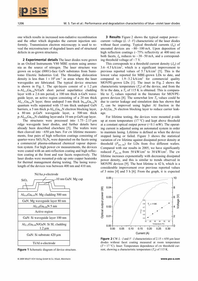
one which results in increased non-radiative recombination and the other which degrades the current injection uni-formity. Transmission electron microscopy is used to re-veal the microstructure of degraded lasers and of structural defects in as-grown structures. 2 Experimental details The laser diodes were grown in an Oxford Instruments V80 MBE system using ammo-nia as the source of nitrogen. The laser structure was grown on n-type (0001)-face GaN substrates from Sumi-tomo Electric Industries Ltd. The threading dislocation density is less than 1 × 106 cm–2 in areas where the laser waveguides are fabricated. The typical device structure is shown in Fig. 1. The epi-layers consist of a 1.2 µm n-Al0.12Ga0.88N/GaN short period superlattice cladding layer with a 2.6 nm period, a 100 nm thick n-GaN wave-guide layer, an active region consisting of a 20 nm thick Al0.11Ga0.89N layer; three undoped 3 nm thick In0.08Ga0.92N quantum wells separated with 15 nm thick undoped GaN barriers, a 5 nm thick p-Al0.2Ga0.8N electron blocking layer, a 80 nm p-GaN waveguide layer, a 500 nm thick p-Al0.05Ga0.95N cladding layer and a 10 nm p-GaN cap layer. The structures were processed into 1.75–2.15 µm ridge waveguide laser diodes, and further details have already been described elsewhere [5]. The wafers were then cleaved into ~650 µm bars. For cw lifetime measure-ments, four pairs of high reflection coatings consisting of quarter-wave SiO2/Si3N4 were deposited on the facets using a commercial plasma-enhanced chemical vapour deposi-tion system. For high power cw measurements, the devices were coated with an anti-reflection coating and high reflec-tion coating at the front and rear facets respectively. The laser diodes were mounted p-side up onto copper heatsinks for thermal management during testing. The lasing wave-length of the devices was between 400 nm and 410 nm.
Ti/Al n-electrode
GaN: Si substrate 420 µm
GaN: Si waveguide layer 100 nm
Al0.12Ga0.88N/GaN: Si SL cladding 1.2 µm
Active region
Al0.20Ga0.80N 5 nm
SiO2 10 nm GaN: Mg cap
Ni/Au p-electrode
GaN: Mg waveguide layer 80 nm
Al0.05Ga0.95N: Mg cladding 500 nm
Figure 1 Schematic diagram of device structure.
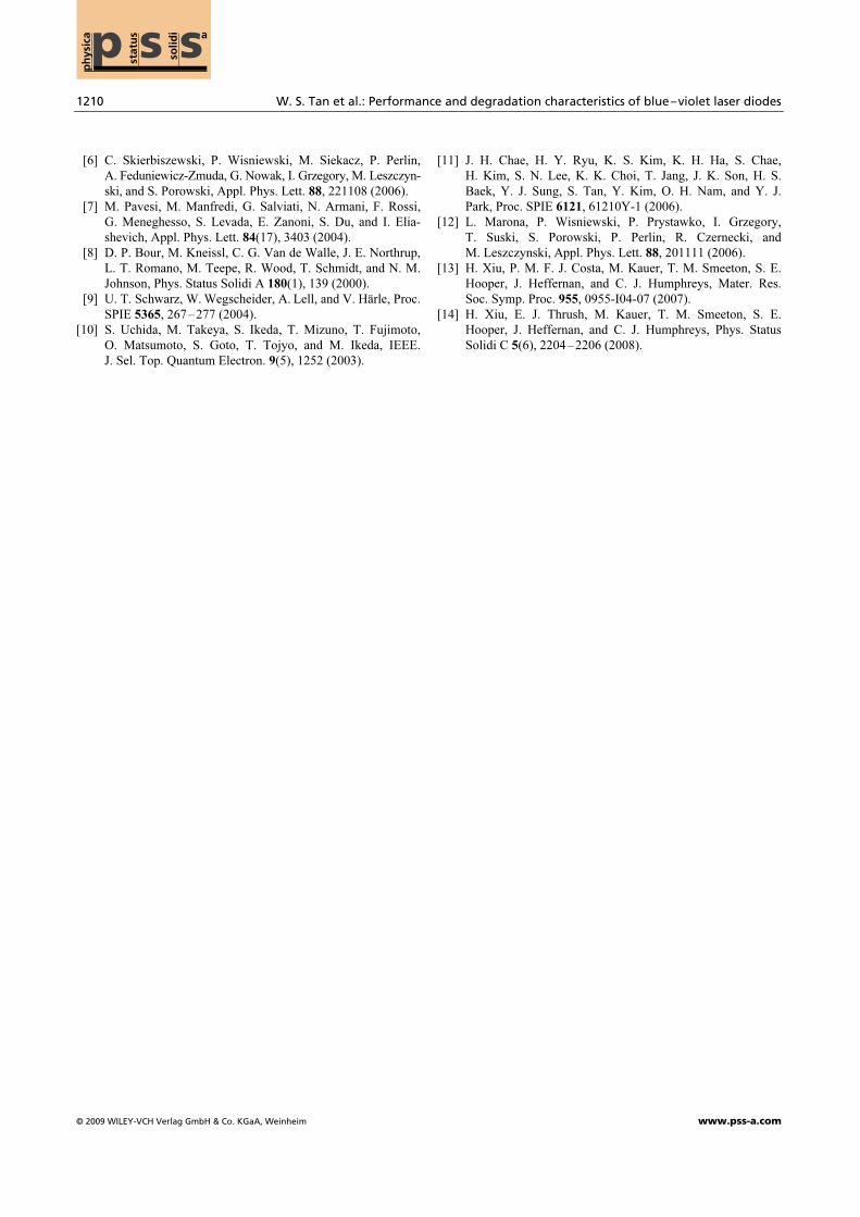
3 Results Figure 2 shows the typical output power–current–voltage (L–I–V) characteristic of the laser diodes without facet coating. Typical threshold currents (Ith) of uncoated devices are ~80–100 mA. Upon deposition of high reflection coatings (~75% reflectivity at 400 nm) on both facets, Ith reduces to ~38–50 mA, and a correspond-ing threshold voltage of ~7 V. This corresponds to a threshold current density (Jth) of 3.6–4.5 kA/cm2, which is a significant improvement to previous reported values of 5.7 kA/cm2 [5]. This is the lowest value reported for MBE-grown LDs to date, and compared to 1.9–3.2 kA/cm2 for commercial quality MOVPE-grown LDs [1]. The inset in Fig. 2 shows the characteristic temperature (T0) of the device, and from the fit to the data, a T0 of 115 K is obtained. This is compara-ble to T0 values reported in the literature for MOVPE-grown devices [8]. The somewhat low T0 values could be due to carrier leakage and simulation data has shown that T0 can be improved using higher Al fraction in the p-Al
xGa1–xN electron blocking layer to reduce carrier leak-
age.
For lifetime testing, the devices were mounted p-side
up at room temperature (17 °C) and kept above threshold
at a constant optical output power (<0.1 mW). The operat-
ing current is adjusted using an automated system in order
to maintain lasing. Lifetime is defined as when the device
stopped lasing or failed. Figure 3 shows the statistical
variation of cw lifetime against dissipated power density at
threshold (Pdiss_Ith) for LDs from five different wafers.
Compared with our results in 2005, we have significantly
reduced Pdiss_Ith from 50 kW/cm2 to 30 kW/cm2. The cw
lifetime increases exponentially with decreasing dissipated
power density, and this is similar to trends observed in
MOVPE devices [9]. The best lifetime is 42 h, which is a
considerable improvement over previous reported values
of 3 mins [4] and 5 h [6]. From the graph, it is expected
10 20 30 40 50 60
4.4
4.5
4.6
4.7
4.8
4.9
ln (
I th)
Temperature (ºC)
T0 = 115K
0.00 0.05 0.10 0.15 0.20 0.25 0.300.00
0.01
0.02
0.03
0.04
0.05
0
2
4
6
8
10V
olta
ge (
V)
Opt
ical
out
put p
ower
(W
)
Current (A)
Figure 2 CW L– I and V– I characteristics of 2.15 × 650 µm laser
diodes without facet coating measured at room temperature
(T = 17 °C). Inset: Temperature dependence of cw threshold cur-
rent, showing a characteristic temperature (T0) of 115 K.

Phys. Status Solidi A 206, No. 6 (2009) 1207
www.pss-a.com © 2009 WILEY-VCH Verlag GmbH & Co. KGaA, Weinheim
Original
Paper
0 20 40 60 800.01
0.1
1
10
100
1000 Wafer 1 Wafer 2 Wafer 3 Wafer 4 Wafer 5
cw la
ser
lifet
ime
(h)
initial cw Pdiss_Ith
(kW/cm2)
Figure 3 CW lifetime of MBE laser diodes against dissipated
power density at the beginning of lifetime test (T = 17 °C). De-
vice dimensions are nominally 1.75–2.15 × 650 µm. The straight
line is a guide to the eye.
that further reduction in the dissipated power will lead to improved LD lifetime. Assuming exponential behaviour, a cw lifetime of ~1000 h can be extrapolated to a Pdiss_Ith of 15–20 kW/cm2. To improve the power performance of the LDs, im-proving the slope efficiency will be essential. This can be achieved by optimizing the internal parameters such as the internal loss and quantum efficiency. Two different struc-tures (structures A and B) were grown by tailoring the p-waveguide Mg-doping profile at the vicinity of the active region in order to reduce the optical absorption. For struc-ture A, the p-waveguide is grown at a constant temperature,
0.00 0.04 0.08 0.12 0.16 0.200.00
0.01
0.02
0.03
0.04
0.05
0.06
Structure A Structure B
Opt
ical
out
put p
ower
(W
)
Current (A)
Figure 4 L– I characteristics of two structures with different
p-waveguide doping profiles. The circle (structure A) and triangle
(structure B) symbols represent the non-graded and graded dop-
ing profile respectively. The device dimensions are 1.8 × 780 µm.
resulting in uniform doping throughout the layer. For struc-ture B, the p-waveguide growth temperature is graded such that the region closest to the p-AlGaN blocking layer is gradually less doped than other regions on the p-waveguide. This is to ensure that high quality p-GaN material is obtained at the region closest to the active re-gion, while gradually increasing the p-doping on regions further away from the active region in order to maintain a good threshold voltage. This method is achieved by gradu-ally ramping down the p-waveguide growth temperature. Figure 4 shows the L–I curves and the slope efficiency for structures A and B are 0.45 W/A and 0.71 W/A respec-tively. The threshold current is significantly reduced from ~110 mA to 70 mA for structure B. The current–voltage characteristics remained similar for both structures. The considerable improvement in threshold current and slope efficiency for structure B suggests that introduction of the graded doping profile have decreased the probability for Mg to diffuse back to the active region. This may increase the non-radiative lifetime, thus increasing the internal quantum efficiency. Another possible explanation is the in-troduction of the graded structure may also reduce the op-tical absorption in the vicinity of the active region, thus reducing the optical loss and subsequently the threshold current. To further investigate the differences in loss between structures A and B, the devices were facet coated. Using the calculated facet reflectivity together with the measured slope efficiency, the internal loss of the devices can be ex-tracted. It is found that the internal loss has decreased from 45 cm–1 in structure A to 15 cm–1 in structure B. The sharp reduction in loss may be attributed to reduced Mg incorpo-ration in the vicinity of the active region and is now com-parable to loss values of ~14 cm–1 in commercial grade MOVPE laser diodes [10]. This result demonstrates that high quality MBE laser diodes with low internal loss have been successfully achieved. To determine the maximum cw output power of struc-ture B, the devices are coated with a high reflection and anti reflection coating (HR-AR) on the front and rear facets respectively. The coating reflectivities are ~75% and 5% at 400 nm for the high reflection and anti reflection layers re-spectively. The sample is mounted p-side up onto a copper heatsink at room temperature during testing. The resulting L–I curve is shown in Fig. 5. A cw slope efficiency of 1.08 W/A is obtained and the maximum cw output power is 145 mW. This result represents the highest output power achieved so far for blue–violet LDs frown by MBE. The kink at 180 mA is due to second order modes, as seen in the far field. The maximum output power is currently lim-ited by thermal dissipation, as this can be observed from the rollover of the L–I curve at 300 mA, which is due to self heating. More efficient thermal dissipation can be achieved by mounting the device p-side down and this is expected to further increase cw lifetime and maximum output power [11]. Higher cw output powers and slope efficiencies beyond 150 mW and 1.1 W/A can also be

1208 W. S. Tan et al.: Performance and degradation characteristics of blue–violet laser diodes
© 2009 WILEY-VCH Verlag GmbH & Co. KGaA, Weinheim www.pss-a.com
ph
ysic
ap s sstat
us
solid
i a
0.00 0.05 0.10 0.15 0.20 0.25 0.30 0.35
0.00
0.02
0.04
0.06
0.08
0.10
0.12
0.14
0.16
Current (A)
Opt
ical
out
put p
ower
(W
)
Figure 5 CW L– I curve of a device coated with high reflection
and anti-reflection coating at the front and rear facets, respectively.
The device dimension is 1.8 × 780 µm.
achieved by further optimization of the high reflection coating from 75% to >90%. The underlying mechanisms towards the degradation of LD characteristics during lifetime testing of nitride LDs are not well understood. Further insight into this phenome-non will be important towards improving reliability for LD commercialization purposes. Device degradation studies in MOVPE LDs have suggested diffusion of point defects through threading dislocations into the active region to be responsible, thus resulting in increased non-radiative re-combination [7, 12]. In the following section, the degrada-tion characteristics of our MBE laser diodes are investi-gated using various techniques. The defects in the p-type layers of aged MBE LDs were initially analysed using transmission electron micro-scopy (TEM). Four major types of defects were observed: cracks, stacking faults (SFs), inversion domains (IDs) and dislocation networks. A significant density of IDs was found in the p-layers of as-grown structures, but there were no changes to these defects after aging [13]. Therefore, the role of IDs remains unclear at present. There were also no structural changes to SFs of untested and tested devices. An interesting observation is the presence of dislocation networks located in the active region of aged devices, since these were not found on untested devices [14]. It is possi-ble that dislocations act as non-radiative recombination centers, thus leading to increased threshold current during lifetime test. These initial TEM studies were carried out on randomly chosen sites of degraded LDs. In the following, we describe our work on site-specific TEM. The use of TEM is typically restricted to small vol-umes of a specimen due to constraints of specimen prepa-ration. In order to obtain a larger scale analysis, µPL and µEL is used to map emissions from the ridge waveguide regions of the LDs. This technique allows the degraded re-
Figure 6 (online colour at: www.pss-a.com) (a) and (b) µPL
maps of LDs tested to failure under cw injection and (c) untested
laser. The intensity scale is normalized to 1 for clarity. The arrow
in map (b) points to the region investigated by TEM.
gions to be identified for TEM analysis. Degraded LDs which have stopped lasing due to high threshold current from lifetime testing were analysed, and an untested device is also measured as a comparison in both cases. For µPL mapping, the p-layer contacts and SiO2 layer were re-moved by dipping in HCL:HNO3 (3:1) and HF respec-tively. The PL signal is obtained by focusing a HeCd laser on the top p-region surface through a 15× microscope ob-jective. The sample is then moved along the stage using properly aligned step motors to generate a surface map. The spatial resolution of the image is ~1–2 µm. Fig-ure 6(a) and (b) show the integrated intensity map of failed LDs, when compared to an untested device (Fig. 6(c)). The dark stripes in Fig. 6(a) to (c) are due to lower PL signal arising from strong laser absorption into the p-AlGaN cladding along the ridge waveguide. Dark regions are ob-served outside the stripe region in Fig. 6(a) and (b), but in contrast, the untested device in Fig. 6(c) did not show any dark regions outside the stripe region. Since optical and scanning electron microscopy images did not reveal any evident defects or damage to the dark regions outside the stripe region of failed LDs in Fig. 6(a) and (b), this sug-gests that they were related to non-radiative recombination in the active region. The microstructure of the dark regions is subsequently investigated by TEM. The area marked by the white arrow in Fig. 6(b) is removed by using focused ion beam milling, leaving a ~300 nm thick membrane in the region of inter-est of the ridge. Bright field TEM images were acquired using a Phillips CM30 operating at 300 kV and the results obtained are shown in Fig. 7. More than ten dislocations are observed in the vicinity of the active region, all of which lie parallel to the (0001) plane and the dislocation array extends for a few micrometers parallel to the ridge direction. The same type of defect was not observed else-where in the device. This is similar to the extent of the re-gion with reduced PL intensity and suggests that the array

Phys. Status Solidi A 206, No. 6 (2009) 1209
www.pss-a.com © 2009 WILEY-VCH Verlag GmbH & Co. KGaA, Weinheim
Original
Paper
Figure 7 (online colour at: www.pss-a.com) Cross-sectional
bright field TEM image taken under two beam conditions with
g = 1120 .· Ò The sample has been tilted by 14° from edge on to re-
veal dislocations lying parallel to the (0001) plane.
of dislocations is the most likely origin of the dark regions. This result demonstrates the usefulness of µPL as a power-ful tool to identity degraded regions in localized areas, which may warrant further TEM analysis. For µEL maps, the bottom emitted EL from the laser under test is obtained by imaging the ridge waveguide through the chip substrate after mechanical polishing of the substrate (resulting in a smooth GaN-air interface). The device is mounted onto a glass slide n-side down and elec-trical injection is achieved by wire bonding. The resolution of EL mapping is limited to tens of microns, which corre-sponds to the lateral dimension of the area from which is the EL signal is collected through a 50× microscope objec-
Figure 8 (online colour at: www.pss-a.com) Bottom emitted
µEL maps of a portion of a laser diode waveguide measured at
different aging periods of the laser life under a constant cw injec-
tion of 5 kA/cm2: (a) untested, (b) aged for 2 hours, (c) aged for
4 hours and (d) aged for 5 hours. (e) µPL map of the same portion
of the waveguide measured after unmounting the laser chip and
after removing the p-contact and SiO2. µPL colour scale is in-
verted for clarity.
tive. This can however be refined down to ~2 µm, by spa-tially filtering the collected signal through the use of a pin-hole. Figure 8(a) to (d) ((a) untested, (b) 2 h, (c) 4 h and (d) 5 h of cw operation) show the maps of the bottom emitted EL taken at different periods of the LD tested under cw conditions at a current density of 5 kA/cm2. It can be seen that the signal intensity is relatively uniform at the early stages of the test, but increasing non-uniformities begin to appear with increasing aging time. Figure 8(e) shows the µPL of the same device measured after 5 h of operation. The colour scale of the µPL map is inverted to show more clearly the uniformity of the emission. The µPL data, in contrast to the µEL shows good uniformity, suggesting that the optical quality of the active region remains undegraded. This indicates that the EL inhomogeneities are related to degradation in current injection and not due to increased non-radiative recombination sites. This effect may be due to defect formation at the interface between metal and p-layers, or to local degradation of the p-AlGaN electron blocking layer resulting in localized carrier leakage. 4 Conclusion In summary, optimization of the active region and p-layer doping has improved the lifetime and power performance of blue–violet LDs grown by MBE. This has resulted in a record cw lifetime of 42 h, cw slope efficiency of 1.08 W/A and a maximum cw output power of 145 mW. The power performance of the LDs represents a significant improvement over previously reported values and highlights the capability of MBE to produce high qual-ity active regions. µPL and µEL have successfully been used to reveal two different types of degradation mecha-nism in the aging behaviour of our devices, the former due to an increase in non-radiative recombination sites and the latter due to increased non uniformities in current injection. TEM analysis of the degraded region obtained from µPL measurements have revealed the formation of dislocations lying in the vicinity of the active region of aged devices. These results have shed more light on the intensely debated aging behaviour of nitride LDs and will be useful for fu-ture device optimization work.
References
[1] S. Nagahama, N. Iwasa, M. Senoh, T. Matsushita, Y. Sugi-
moto, H. Kiyoku, T. Kozaki, M. Sano, H. Matsumura,
H. Uemoto, K. Chocho, and T. Mukai, Jpn. J. Appl. Phys.
39, L647–L650 (2000).
[2] T. Tojyo, T. Asano, M. Takeya, T. Hino, S. Kijima, S. Goto,
S. Uchida, and M. Ikeda, Jpn. J. Appl. Phys. 40, 3206 (2001).
[3] S. Rajan, P. Waltereit, C. Poblenz, S. J. Heikman, D. S.
Green, J. S. Speck, and U. K Mishra, IEEE Electron Device
Lett. 25, 247 (2004).
[4] M. Kauer, S. E. Hooper, V. Bousquet, K. Johnson, C. Zell-
weger, J. M. Barnes, J. Windle, T. M. Smeeton, and J. Hef-
fernan, Electron. Lett. 41, 739 (2005).
[5] M. Kauer, V. Bousquet, S. E. Hooper, J. M. Barnes, J. Win-
dle, W. S. Tan, and J. Heffernan, Phys. Status Solidi A
204(1), 221 (2007).
1210 W. S. Tan et al.: Performance and degradation characteristics of blue–violet laser diodes
© 2009 WILEY-VCH Verlag GmbH & Co. KGaA, Weinheim www.pss-a.com
ph
ysic
ap s sstat
us
solid
i a
[6] C. Skierbiszewski, P. Wisniewski, M. Siekacz, P. Perlin,
A. Feduniewicz-Zmuda, G. Nowak, I. Grzegory, M. Leszczyn-
ski, and S. Porowski, Appl. Phys. Lett. 88, 221108 (2006).
[7] M. Pavesi, M. Manfredi, G. Salviati, N. Armani, F. Rossi,
G. Meneghesso, S. Levada, E. Zanoni, S. Du, and I. Elia-
shevich, Appl. Phys. Lett. 84(17), 3403 (2004).
[8] D. P. Bour, M. Kneissl, C. G. Van de Walle, J. E. Northrup,
L. T. Romano, M. Teepe, R. Wood, T. Schmidt, and N. M.
Johnson, Phys. Status Solidi A 180(1), 139 (2000).
[9] U. T. Schwarz, W. Wegscheider, A. Lell, and V. Härle, Proc.
SPIE 5365, 267–277 (2004).
[10] S. Uchida, M. Takeya, S. Ikeda, T. Mizuno, T. Fujimoto,
O. Matsumoto, S. Goto, T. Tojyo, and M. Ikeda, IEEE.
J. Sel. Top. Quantum Electron. 9(5), 1252 (2003).
[11] J. H. Chae, H. Y. Ryu, K. S. Kim, K. H. Ha, S. Chae,
H. Kim, S. N. Lee, K. K. Choi, T. Jang, J. K. Son, H. S.
Baek, Y. J. Sung, S. Tan, Y. Kim, O. H. Nam, and Y. J.
Park, Proc. SPIE 6121, 61210Y-1 (2006).
[12] L. Marona, P. Wisniewski, P. Prystawko, I. Grzegory,
T. Suski, S. Porowski, P. Perlin, R. Czernecki, and
M. Leszczynski, Appl. Phys. Lett. 88, 201111 (2006).
[13] H. Xiu, P. M. F. J. Costa, M. Kauer, T. M. Smeeton, S. E.
Hooper, J. Heffernan, and C. J. Humphreys, Mater. Res.
Soc. Symp. Proc. 955, 0955-I04-07 (2007).
[14] H. Xiu, E. J. Thrush, M. Kauer, T. M. Smeeton, S. E.
Hooper, J. Heffernan, and C. J. Humphreys, Phys. Status
Solidi C 5(6), 2204–2206 (2008).