performance analysis of trench power mosfets in …downloads.hindawi.com/archive/2008/412175.pdf ·...
TRANSCRIPT
Hindawi Publishing CorporationInternational Journal of Power Management ElectronicsVolume 2008, Article ID 412175, 9 pagesdoi:10.1155/2008/412175
Research ArticlePerformance Analysis of Trench Power MOSFETs inHigh-Frequency Synchronous Buck Converter Applications
Yali Xiong,1 Xu Cheng,2 Xiangcheng Wang,3 Pavan Kumar,4 Lina Guo,1 and Z. John Shen1
1 School of Electrical Engineering and Computer Science, University of Central Florida, Orlando, P.O. Box 162362, FL 32816, USA2 Freescale Semiconductor, Tempe, AZ, USA3 Cherokee International, Santa Ana, CA, USA4 Intel Corporation, Hillsboro, Oregon, USA
Correspondence should be addressed to Z. John Shen, [email protected]
Received 3 January 2008; Accepted 7 March 2008
Recommended by Peter Barbosa
This paper investigates the performance perspectives and theoretical limitations of trench power MOSFETs in synchronous rectifierbuck converters operating in the MHz frequency range. Several trench MOSFET technologies are studied using a mixed-modedevice/circuit modeling approach. Individual power loss contributions from the control and synchronous MOSFETs, and theirdependence on switching frequency between 500 kHz and 5 MHz are discussed in detail. It is observed that the conductionloss contribution decreases from 40% to 4% while the switching loss contribution increases from 60% to 96% as the switchingfrequency increases from 500 KHz to 5 MHz. Beyond 1 MHz frequency there is no obvious benefit to increase the die size of eitherSyncFET or CtrlFET. The RDS(ON) × QG figure of merit (FOM) still correlates well to the overall converter efficiency in the MHzfrequency range. The efficiency of the hard switching buck topology is limited to 80% at 2 MHz and 65% at 5 MHz even with themost advanced trench MOSFET technologies.
Copyright © 2008 Yali Xiong et al. This is an open access article distributed under the Creative Commons Attribution License,which permits unrestricted use, distribution, and reproduction in any medium, provided the original work is properly cited.
1. INTRODUCTION
Trench powerMOSFETsare widely used as both control andsynchronous rectifier switches (CtrlFET and SyncFET) inbuck converters for computer, telecommunication, and con-sumer applications [1–5]. Power MOSFETs usually accountfor most of the power losses, and often determine theoverall efficiency of today’s DC/DC converters. Over the pastdecade, the power semiconductor industry has significantlyimproved MOSFET performance, especially in terms of thefigure of merit (FOM) of RDS(ON) × QG [6, 7]. The analysis,modeling, and optimization of power MOSFET performancein synchronous buck converters have also become the focusof a significant amount of research work in the past few years[8–12]. The objective is to identify the optimum design ofthe CtrlFETs and SyncFETs that offer the highest converterefficiency. The previous work addressed this goal withvaried levels of success, but several issues still remain openespecially in light of ever-evolving DC/DC converter designrequirements.
The RDS(ON) × QG FOM is generally considered as thesingle most important indicator of MOSFET performance inDC/DC converters in the medium switching frequency rangeof 100 kHz to 1 MHz. As the switching frequency of buckconverters increases to the MHz range to facilitate better con-verter transient response and smaller passive components, itis, however, not clear how closely the RDS(ON) × QG FOMcorrelates to the overall converter efficiency, or whether ornot a different FOM needs to be defined. Furthermore, theanalysis on individual MOSFET power loss contributions,namely, conduction loss of the CtrlFET, conduction lossof the SyncFET, switching loss of the CtrlFET, diode lossof the SyncFET, and gate-drive losses of both the CtrlFETand SyncFET, was previously limited to the use of simpleanalytical equations based on approximations and assump-tions [4, 8, 9, 11, 13]. These simple device models have onlyvery limited accuracy [14]. More importantly, they are notcapable of revealing or predicting the influence of variationsin device structures or circuit operating conditions on eachof the individual power loss terms. This is the essential

2 International Journal of Power Management Electronics
knowledge required for developing future generation powerMOSFETs for high-efficiency and high-density buck con-verters. Lastly, the scope of the previous work on powerMOSFET performance analysis was limited to the study ofeither one particular power MOSFET technology [4] or justa limited number of commercial parts [5, 15]. While offeringuseful information on how to select commercially availablepower MOSFETs for today’s practical converter design, theprevious work does not sufficiently address the perspectivesand theoretical limitations of power MOSFET technologyfor future generation DC/DC converters operating withever-increasing switching frequency, slew rate, and outputcurrent.
The purpose of this paper is to comprehensively inves-tigate the performance perspectives and theoretical limita-tions of trench power MOSFET technology in synchronousrectifier buck converters over a wide range of operatingconditions [16]. The MOSFET device structures underinvestigation include but are not limited to those manufac-turable with today’s semiconductor fabrication technology.The investigation was carried out with a mixed-modedevice/circuit simulation approach. Device measurementdata was also used to validate the physical device models.Various power loss contributions from the CtrlFETs andSyncFETs at different operating conditions were studied indetail. Several important observations were made which mayshed some light on the development of future generationpower MOSFETs, as well as the optimal utilization of today’spower MOSFETs in buck converter applications.
2. METHODOLOGY
Although the efficiency of a buck converter is usuallydetermined by directly measuring its input and outputpower, such an experimental approach proves very diffi-cult to employ to characterize the individual power lossterms of the control and sync FETs in the converter. Theactual current waveforms, and to a less extent, the voltagewaveforms, of the power MOSFETs in a high-current, high-slew rate DC/DC converter are most likely disturbed by themeasurement setup such as current probe loops, resultingin large distortions and measurment errors. The limitedsampling rate of digital oscilloscopes often introduces somemeasurement errors as well. Modeling analysis approachesprovide an alternative way of investigating power MOSFETperformance in buck converters.
The previous work on power MOSFET performanceanalysis used simple analytical device models to calculateRDS(ON), QG, and other device parameters, and a set ofsimple analytical equations for power loss calculation [4, 8,11, 13]. While these approaches provide a quick first-orderestimation of converter efficiency, its accuracy is inevitablylimited by the approximation and simplification made in theanalytical models. Recently, Cavallaro et al. used a circuitsimulator to estimate buck converter power losses usingMOSFET behavior models which were derived from two-dimensional numerical device and process simulation [9].It should be pointing out that the accuracy of converterpower losses can be further improved by using a mixed-mode
CtrlFET
Syn
cFE
TRg
Rg
L
Vin VoutC
Figure 1: Mixed-mode DESISS simulations for DC/DC converterwith numerical power MOSFET models.
device/circuit simulation approach with numerical MOSFETmodels being directly incorporated into circuit simulation.Furthermore, detailed information on various power losscontributions of the CtrlFETs and SyncFETs over a widerange of operating conditions can be easily obtained fromthe mixed-mode simulation.
In this paper, we used a physically based mixeddevice/circuit modeling approach to investigate the powerlosses of the MOSFETs under different operating condi-tions. “Virtual” power MOSFETs were first built usinga two-dimensional numerical device simulation TCADtool-DESSIS from Synopsis [17], and then placed into a12 V-to-1 V, 20 A buck converter circuit for mixed-modedevice/circuit simulation. Figure 1 depicts the concept of thisapproach. DESSIS numerically solves the Possion’s equation,the continuity equations of electron and hole currents self-consistently, using a variety of physical models. It can beused to predict the electrical characteristics of arbitrarytwo- or three-dimensional semiconductor structures underuser-specified operating conditions. It also offers SPICE-like circuit simulation capability combined with devicenumerical modeling capability, and provides a quick andinexpensive way of evaluating and optimizing circuit anddevice concepts. Unlike analytical or other SPICE models ofpower MOSFETs, the numerical device model, relying littleon approximations or simplifications, faithfully representsthe behavior of a realistic power MOSFET, and providesphysical insights on device operation. Note that while thismixed device/circuit modeling method is suitable for ourstudy of power MOSFET losses, it is not convenient to usefor general circuit design purposes.
3. MODELING OF BASIC TRENCH POWER MOSFET
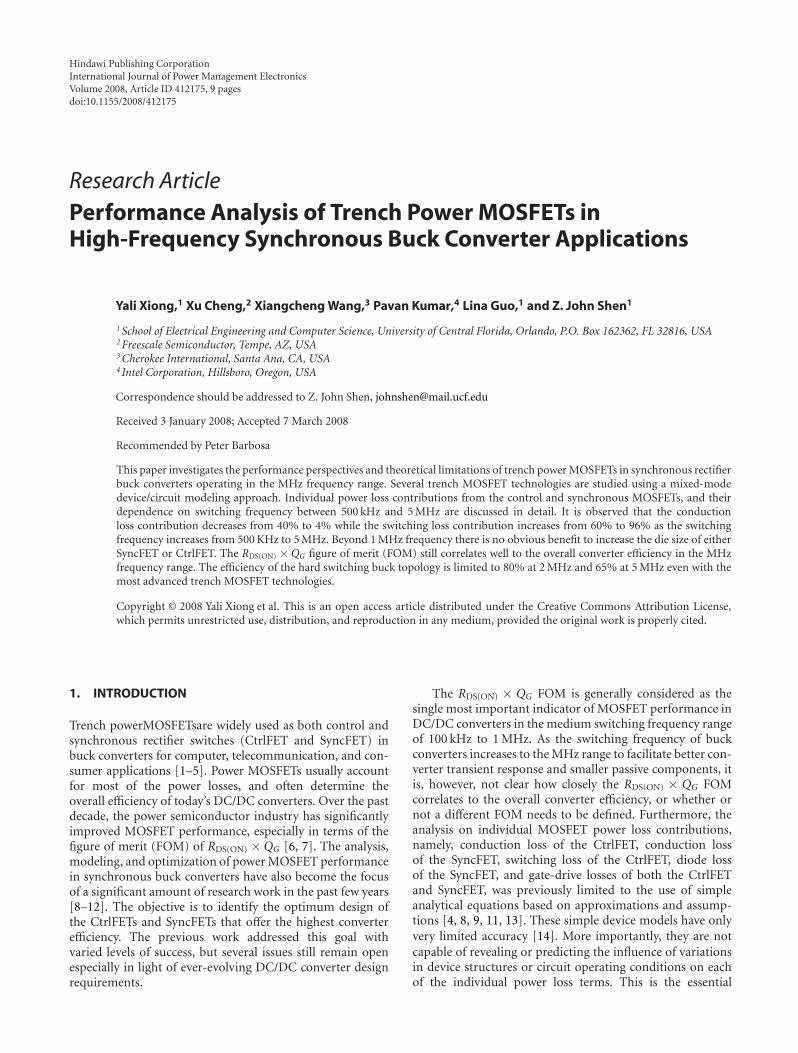
A basic trench MOSFET structure with a cell pitch of2.5 μm is shown in Figure 2. To accurately reproduce thebehavior of the trench MOSFETs in real circuit operation,we have carefully chosen the physical models and modelparameters used in DESSIS simulation, such as carriermobility and lifetime. The trench MOSFET model wasvalidated by comparing to measurement data of real devices.Table 1 shows the electrical parameter comparison betweenthe “virtual” trench power MOSFET and its real worldcounterpart. Reasonable agreement is observed.
Yali Xiong et al. 3
Table 1: Comparison of simulated and measured electrical param-eters of the basic trench power MOSFET.
Device parametersBasic trench MOSFET
Modeled (type A) Measured (IR6618)
BVDSS @250 μA (V) 36.4 33
VTH @250 μA (V) 1.35 1.7
RDS(on) @4.5 V (mΩ) 2.3 3.2
QG @4.5 V/15 V (nC) 43 45
QGD @15 V (nC) 15 15
Qrr @100 A/μs (nC) 33.5 46
n+n+
Polygate p-
bodyp-
body
n-epi
Figure 2: A basic trench power MOSFET structure (type A).
After the completion of MOSFET phsical models valida-tion, a chip set ofvirtualCtrlFET and SyncFET is incorpo-rated into the mixed-mode simulation of a buck convertercircuit with an input voltage of 12 V and an output voltageand current of 1 V and 20 A, respectively, in Figure 1. Theduty cycle of the buck converter was carefully adjusted tomaintain the 1 V/20 A output. An RDS(ON) ratio of 4.3 waschosen between the CtrlFET and SyncFET. The issue ofoptimizing this RDS(ON) ratio is to be discussed in Section 5.
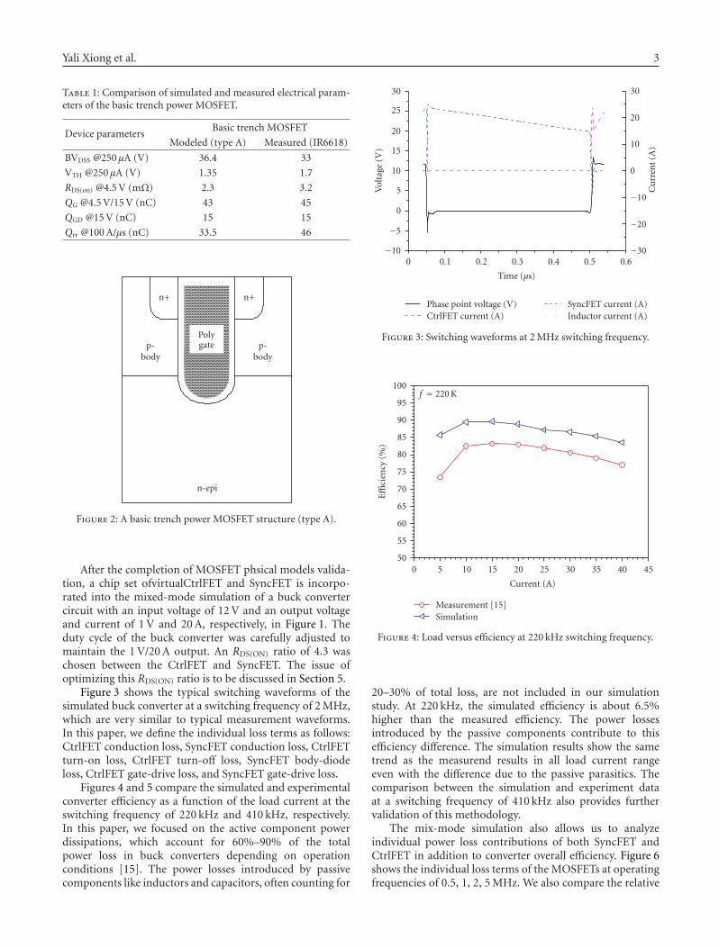
Figure 3 shows the typical switching waveforms of thesimulated buck converter at a switching frequency of 2 MHz,which are very similar to typical measurement waveforms.In this paper, we define the individual loss terms as follows:CtrlFET conduction loss, SyncFET conduction loss, CtrlFETturn-on loss, CtrlFET turn-off loss, SyncFET body-diodeloss, CtrlFET gate-drive loss, and SyncFET gate-drive loss.
Figures 4 and 5 compare the simulated and experimentalconverter efficiency as a function of the load current at theswitching frequency of 220 kHz and 410 kHz, respectively.In this paper, we focused on the active component powerdissipations, which account for 60%–90% of the totalpower loss in buck converters depending on operationconditions [15]. The power losses introduced by passivecomponents like inductors and capacitors, often counting for
0.60.50.40.30.20.10
Time (μs)
−10
−5
0
5
10
15
20
25
30
Vol
tage
(V)
Phase point voltage (V)CtrlFET current (A)
SyncFET current (A)Inductor current (A)
−30
−20
−10
0
10
20
30
Cu
rren
t(A
)
Figure 3: Switching waveforms at 2 MHz switching frequency.
454035302520151050
Current (A)
50
55
60
65
70
75
80
85
90
95
100E
ffici
ency
(%)
Measurement [15]Simulation
f = 220 K
Figure 4: Load versus efficiency at 220 kHz switching frequency.
20–30% of total loss, are not included in our simulationstudy. At 220 kHz, the simulated efficiency is about 6.5%higher than the measured efficiency. The power lossesintroduced by the passive components contribute to thisefficiency difference. The simulation results show the sametrend as the measurend results in all load current rangeeven with the difference due to the passive parasitics. Thecomparison between the simulation and experiment dataat a switching frequency of 410 kHz also provides furthervalidation of this methodology.
The mix-mode simulation also allows us to analyzeindividual power loss contributions of both SyncFET andCtrlFET in addition to converter overall efficiency. Figure 6shows the individual loss terms of the MOSFETs at operatingfrequencies of 0.5, 1, 2, 5 MHz. We also compare the relative

4 International Journal of Power Management Electronics
454035302520151050
Current (A)
50
55
60
65
70
75
80
85
90
95
100
Effi
cien
cy(%
)
Measurement [15]Simulation
f = 410 kHz
Figure 5: Load versus efficiency at 410 kHz switching frequency.
543210
Frequency (MHz)
0
0.5
1
1.5
2
2.5
3
3.5
4
Pow
erlo
ss(W
)
CtrlFET conduction lossSyncFET conduction lossCtrlFET turn-on lossCtrlFET turn-off lossSyncFET body-diode lossCtrlFET gate-driver lossSyncFET gate-driver loss
Figure 6: Individual power-loss terms versus switching frequency.
contribution of each power loss term at the switching of0.5 MHz and 5 MHz at Figure 7. The following are observed.
(I) The gate-drive loss of the SyncFET becomes signifi-cant beyond 2 MHz operating frequency. At 5 MHz,the gate-driver loss is about 2 W, or roughly 14% ofthe total power loss.
(II) Conduction losses remain constant independent ofswitching frequency, and count for a small percentageof the total power loss in the MHz frequency range.At 0.5 MHz, the conduction losses account for 40%
f = 0.5 MHz
16%
24%
6%< 1%
22%
22%
9%
CtrlFET conduction lossSyncFET conduction lossCtrlFET turn-on lossCtrlFET turn-off lossSyncFET body-diode lossCtrlFET gate-driving lossSyncFET gate-driving loss
(a)
f = 5 MHz2% 2%
24%
14%
2%
28%
28%
CtrlFET conduction lossSyncFET conduction lossCtrlFET turn-on lossCtrlFET turn-off lossSyncFET body-diode lossCtrlFET gate-driving lossSyncFET gate-driving loss
(b)
Figure 7: Contribution of power losses at switching frequency: (a)0.5 MHz; (b) 5 MHz.
of total power loss, while they only account for 4% oftotal power loss at a switching frequency of 5 MHz.
(III) CtrlFET switching loss and SyncFET body-diode lossdominate the total power loss in the MHz frequencyrange, accounting for roughly 52% and 26% ofthe total power loss at 5 MHz. For the switching

Yali Xiong et al. 5
13121110987654
SyncFET die size (mm2)
50
55
60
65
70
75
80
85
90
95
100
Effi
cien
cy(%
)
0.5 MHz1 MHz
2 MHz5 MHz
CtrlFET die size: 2.2 mm2
Figure 8: Converter efficiency as a function of the SyncFET die size.
frequency of 0.5 MHz and 5 MHz, the total switchinglosses account for 60% and 96% of total power losses,respectively.
Since the individual loss terms are dependent on thesizing of both the CtrlFET and SyncFET [4]. Next, we willfocus on the optimal sizing of CtrlFETs and SyncFETs forbuck converter efficiency.
4. OPTIMAL SIZING OF CONTROL ANDSYNCHRONOUS RECTIFIER MOSFETs
Selection of large-size MOSFETs may not necessarily leadto efficiency improvement since the MOSFET switchingand gate-drive losses increase with increasing die size eventhough the conduction losses are reduced. Silicon cost isyet another factor that needs to be considered in MOSFETsizing. An optimal size exists for both the CtrlFETs andSyncFETs to provide a minimum total power loss.
Figure 8 shows the converter efficiency as a functionof the die size of the SyncFETs given a fixed CtrlFET diesize of 2.2 mm2 at various switching frequencies. The directobservation is that there is no any efficiency benefit byincresing SyncFET die size as frequency beyond 2 MHz.For lower-frequency range, the SyncFET die size increaseintroduces subtle efficiency increase, which is very cost-consuming. For example, at 0.5 MHz, the increase of die sizeabout 2.6 times just results in 2.5% efficiency improvement.For the frequency higher than 2 MHz, such as 5 MHz, thedie size increase, in fact, introduces efficiency degradation.Figure 10 illustrates the individual loss terms at differentfrequencies, which helps to explain the above observations.The switching losses dominate at MHz frequency range,which increases when the switching frequency increases.As the die size increases, the conduction loss decrease iseasily overshadowed by the increase of switching losses. Thiseffect is even more significant for the CtrlFET die sizing.As Figure 9 shows that beyond 1 MHz frequency there is
3.532.521.51
CtrlFET die size (mm2)
50
60
70
80
90
100
Effi
cien
cy(%
)
0.5 MHz1 MHz
2 MHz5 MHz
SyncFET die size: 9.4 mm2
Figure 9: Converter efficiency as a function of the CtrlFET die size.
SyncFETgate-driver
loss
CtrlFETgate-driver
loss
Body-diodeloss
CtrlFETturn-off
loss
CtrlFETturn-on
loss
SyncFETconduction
loss
CtrlFETconduction
loss
0
0.5
1
1.5
2
2.5
3
3.5
4Po
wer
loss
(W)
0.5 MHz1 MHz
2 MHz5 MHz
Figure 10: Individual loss-term comparison over 0.5 to 5 MHz.
already no benefit to increase CtrlFET die size. At 5 MHz, theincreased die size introduces 7% efficiency degradation.
In this specfic case, for a fixed die size of 2.2 mm2 ofthe CtrlFET, the optimal size of the sync-FET decreasesfrom 11.8 mm2 to 4.8 mm2 when the switching frequencyincreases from 500 kHz to 5 MHz, indicating the increasingweight of switching losses at higher switching frequencies.The die size of 9.4 mm2 seems to be a good choice for theSyncFET over the frequency range of 500 kHz to 5 MHz. Fora fixed die size of 9.4 mm2 for the SyncFET, the optimal sizeof the CtrlFET is about 1.1 mm2. The increase in die sizebeyond 3.3 mm2 only results in less than 1% improvementin efficiency at 0.5 MHz, making 1.1 mm2 a good choice forthe CtrlFET.
Furthermore, as shown in Figures 8 and 9, an optimumrange instead of a single maximum point of MOSFET die size
6 International Journal of Power Management Electronics
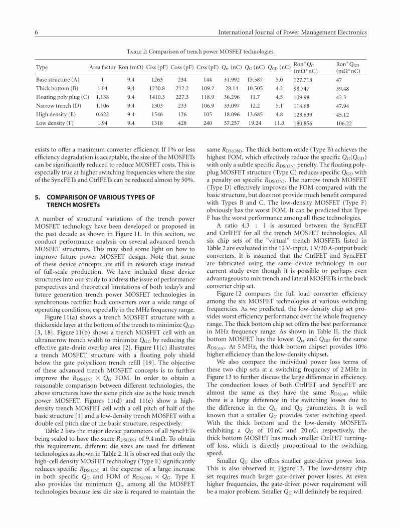
Table 2: Comparison of trench power MOSFET technologies.
Type Area factor Ron (mΩ) Ciss (pF) Coss (pF) Crss (pF) Qrr (nC) QG (nC) QGD (nC) Ron∗QG
(mΩ∗nC)Ron∗QGD
(mΩ∗nC)
Base structure (A) 1 9.4 1263 234 144 31.992 13.587 5.0 127.718 47
Thick bottom (B) 1.04 9.4 1230.8 212.2 109.2 28.14 10.505 4.2 98.747 39.48
Floating poly plug (C) 1.138 9.4 1410.3 227.3 118.9 36.296 11.7 4.5 109.98 42.3
Narrow trench (D) 1.106 9.4 1303 233 106.9 33.097 12.2 5.1 114.68 47.94
High density (E) 0.622 9.4 1546 126 105 18.096 13.685 4.8 128.639 45.12
Low density (F) 1.94 9.4 1318 428 240 57.257 19.24 11.3 180.856 106.22
exists to offer a maximum converter efficiency. If 1% or lessefficiency degradation is acceptable, the size of the MOSFETscan be significantly reduced to reduce MOSFET costs. This isespecially true at higher switching frequencies where the sizeof the SyncFETs and CtrlFETs can be reduced almost by 50%.
5. COMPARISON OF VARIOUS TYPES OFTRENCH MOSFETs
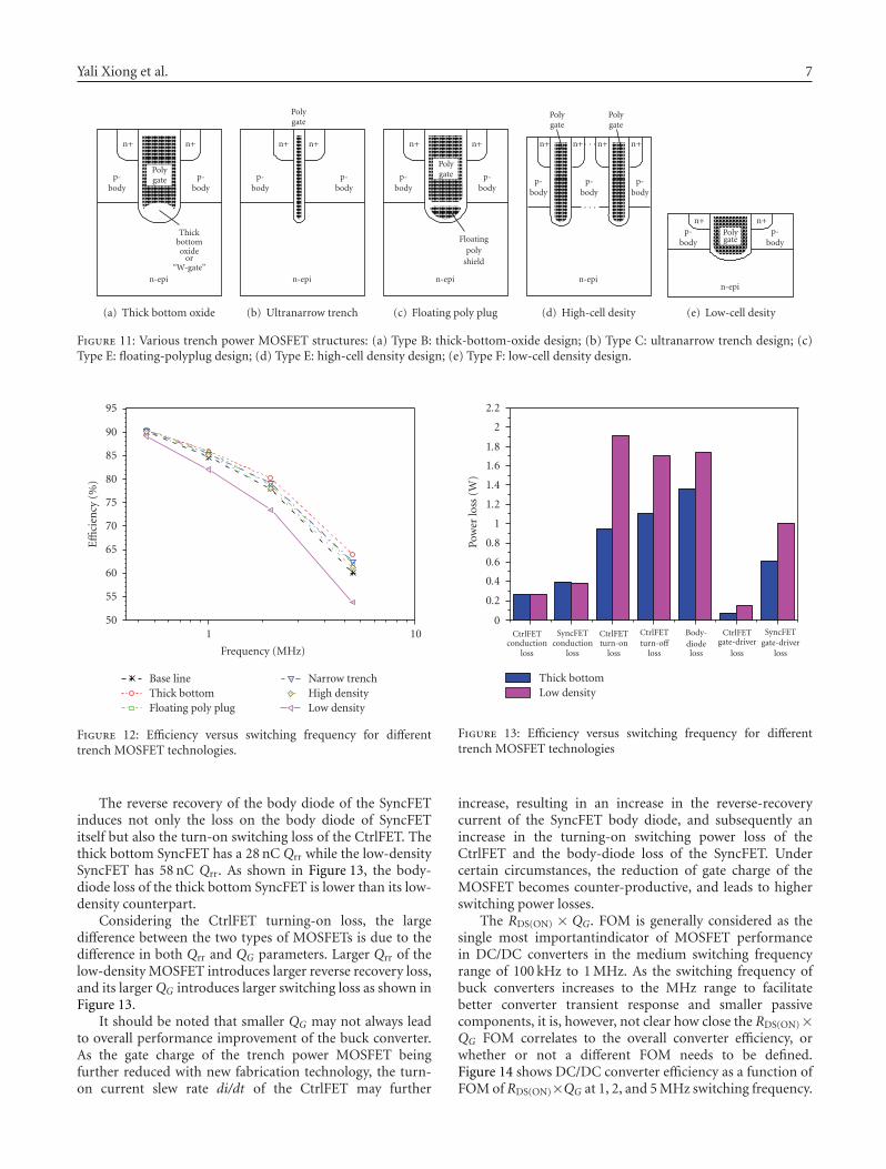
A number of structural variations of the trench powerMOSFET technology have been developed or proposed inthe past decade as shown in Figure 11. In this seciton, weconduct performance analysis on several advanced trenchMOSFET structures. This may shed some light on how toimprove future power MOSFET design. Note that someof these device concepts are still in research stage insteadof full-scale production. We have included these devicestructures into our study to address the issue of performanceperspectives and theoretical limitations of both today’s andfuture generation trench power MOSFET technologies insynchronous rectifier buck converters over a wide range ofoperating conditions, especially in the MHz frequency range.
Figure 11(a) shows a trench MOSFET structure with athickoxide layer at the bottom of the trench to minimize QGD
[3, 18]. Figure 11(b) shows a trench MOSFET cell with anultranarrow trench width to minimize QGD by reducing theeffective gate-drain overlap area [2]. Figure 11(c) illustratesa trench MOSFET structure with a floating poly shieldbelow the gate polysilicon trench refill [19]. The objectiveof these advanced trench MOSFET concepts is to furtherimprove the RDS(ON) × QG FOM. In order to obtain areasonable comparison between different technologies, theabove structures have the same pitch size as the basic trenchpower MOSFET. Figures 11(d) and 11(e) show a high-density trench MOSFET cell with a cell pitch of half of thebasic structure [1] and a low-density trench MOSFET with adouble cell pitch size of the basic structure, respectively.
Table 2 lists the major device parameters of all SyncFETsbeing scaled to have the same RDS(ON) of 9.4 mΩ. To obtainthis requirement, different die sizes are used for differenttechnologies as shown in Table 2. It is observed that only thehigh-cell density MOSFET technology (Type E) significantlyreduces specific RDS(ON) at the expense of a large increasein both specific QG and FOM of RDS(ON) × QG. Type Ealso provides the minimum Qrr among all the MOSFETtechnologies because less die size is requred to maintain the
same RDS(ON). The thick bottom oxide (Type B) achieves thehighest FOM, which effectively reduce the specific QG(QGD)with only a subtle specific RDS(ON) penelty. The floating poly-plug MOSFET structure (Type C) reduces specific QGD witha penalty on specific RDS(ON). The narrow trench MOSFET(Type D) effectively improves the FOM compared with thebasic structure, but does not provide much benefit comparedwith Types B and C. The low-density MOSFET (Type F)obviously has the worst FOM. It can be predicted that TypeF has the worst performance among all these technologies.
A ratio 4.3 : 1 is assumed between the SyncFETand CtrlFET for all the trench MOSFET technologies. Allsix chip sets of the “virtual” trench MOSFETs listed inTable 2 are evaluated in the 12 V-input, 1 V/20 A-output buckconverters. It is assumed that the CtrlFET and SyncFETare fabricated using the same device technology in ourcurrent study even though it is possible or perhaps evenadvantageous to mix trench and lateral MOSFETs in the buckconverter chip set.
Figure 12 compares the full load converter efficiencyamong the six MOSFET technologies at various switchingfrequencies. As we predicted, the low-density chip set pro-vides worst efficiency performance over the whole frequencyrange. The thick bottom chip set offers the best performancein MHz frequency range. As shown in Table II, the thickbottom MOSFET has the lowest Qrr and QGD for the sameRDS(on). At 5 MHz, the thick bottom chipset provides 10%higher efficiency than the low-density chipset.
We also compare the individual power loss terms ofthese two chip sets at a switching frequency of 2 MHz inFigure 13 to further discuss the large difference in efficiency.The conduction losses of both CtrlFET and SyncFET arealmost the same as they have the same RDS(on) whilethere is a large difference in the switching losses due tothe difference in the Qrr and QG parameters. It is wellknown that a smaller QG provides faster switching speed.With the thick bottom and the low-density MOSFETsexhibiting a QG of 10 nC and 20 nC, respectively, thethick bottom MOSFET has much smaller CtrlFET turning-off loss, which is directly proportional to the switchingspeed.
Smaller QG also offers smaller gate-driver power loss.This is also observed in Figure 13. The low-density chipset requires much larger gate-driver power losses. At evenhigher frequencies, the gate-driver power requirement willbe a major problem. Smaller QG will definitely be required.
Yali Xiong et al. 7
n+n+
Polygate
Thickbottomoxide
or“W-gate”
p-body
p-body
n-epi
(a) Thick bottom oxide
n+n+
Polygate
p-body
p-body
n-epi
(b) Ultranarrow trench
n+n+
Polygate
Floatingpoly
shield
p-body
p-body
n-epi
(c) Floating poly plug
n+n+ n+n+· · ·
p-body
Polygate
Polygate
· · ·
p-body
p-body
n-epi
(d) High-cell desity
n+n+p-
bodyp-
body
n-epi
Polygate
(e) Low-cell desity
Figure 11: Various trench power MOSFET structures: (a) Type B: thick-bottom-oxide design; (b) Type C: ultranarrow trench design; (c)Type E: floating-polyplug design; (d) Type E: high-cell density design; (e) Type F: low-cell density design.
101
Frequency (MHz)
50
55
60
65
70
75
80
85
90
95
Effi
cien
cy(%
)
Base lineThick bottomFloating poly plug
Narrow trenchHigh densityLow density
Figure 12: Efficiency versus switching frequency for differenttrench MOSFET technologies.
The reverse recovery of the body diode of the SyncFETinduces not only the loss on the body diode of SyncFETitself but also the turn-on switching loss of the CtrlFET. Thethick bottom SyncFET has a 28 nC Qrr while the low-densitySyncFET has 58 nC Qrr. As shown in Figure 13, the body-diode loss of the thick bottom SyncFET is lower than its low-density counterpart.
Considering the CtrlFET turning-on loss, the largedifference between the two types of MOSFETs is due to thedifference in both Qrr and QG parameters. Larger Qrr of thelow-density MOSFET introduces larger reverse recovery loss,and its largerQG introduces larger switching loss as shown inFigure 13.
It should be noted that smaller QG may not always leadto overall performance improvement of the buck converter.As the gate charge of the trench power MOSFET beingfurther reduced with new fabrication technology, the turn-on current slew rate di/dt of the CtrlFET may further
SyncFETgate-driver
loss
CtrlFETgate-driver
loss
Body-diodeloss
CtrlFETturn-off
loss
CtrlFETturn-on
loss
SyncFETconduction
loss
CtrlFETconduction
loss
0
0.2
0.4
0.6
0.8
1
1.2
1.4
1.6
1.8
2
2.2
Pow
erlo
ss(W
)
Thick bottomLow density
Figure 13: Efficiency versus switching frequency for differenttrench MOSFET technologies
increase, resulting in an increase in the reverse-recoverycurrent of the SyncFET body diode, and subsequently anincrease in the turning-on switching power loss of theCtrlFET and the body-diode loss of the SyncFET. Undercertain circumstances, the reduction of gate charge of theMOSFET becomes counter-productive, and leads to higherswitching power losses.
The RDS(ON) × QG. FOM is generally considered as thesingle most importantindicator of MOSFET performancein DC/DC converters in the medium switching frequencyrange of 100 kHz to 1 MHz. As the switching frequency ofbuck converters increases to the MHz range to facilitatebetter converter transient response and smaller passivecomponents, it is, however, not clear how close the RDS(ON)×QG FOM correlates to the overall converter efficiency, orwhether or not a different FOM needs to be defined.Figure 14 shows DC/DC converter efficiency as a function ofFOM of RDS(ON)×QG at 1, 2, and 5 MHz switching frequency.

8 International Journal of Power Management Electronics
200180160140120100
Ron ∗Qg (Ω∗nC)
50
55
60
65
70
75
80
85
90
Effi
cien
cy(%
)
1 MHz2 MHz5 MHz
Figure 14: FOM RDS(ON) ×QG of trench power MOSFETs.
Different data points in Figure 14 may represent differenttrench MOSFET technologies. The RDS(ON)×QG. FOM seemsto correlate well with the converter efficiency even in theMHz operating frequency range.
6. CONCLUSIONS
In this paper, we have comprehensively investigated the per-formance perspectives and theoretical limitations of trenchpower MOSFETs in synchronous rectifier buck convertersover a wide range of operating conditions. Several trenchMOSFET technologies are investigated using a mixed-modedevice/circuit modeling approach. Individual power losscontributions from the CtrlFETs and SyncFETs and theirdependence on switching frequency between 500 kHz and5 MHz are discussed in detail.
It is observed that going from 0.5 MHz to 5 MHz, theconduction loss contribution decreases from 40% to 4%while the switching loss contribution increases from 60% to96%. Under hard switching operation condition, the buckconverter efficiency is limited to 80% at 2 MHz and 65%at 5 MHz even with the most advanced trench MOSFETtechnology.
For the base technology we studied, beyond 1 MHzfrequency, there is no obvious benefit to increase the die sizeof either SyncFET or CtrlFET. For 5 MHz, given a constantdie size of SyncFETs, the die size increase of CtrlFETs actuallyintroduces obvious efficiency degradation.
For different trench technologies, the technology,whichhas the lowest QG, provides smallest gate-driver lossesand the smallest CtrlFET turning-off losses. On the otherhand, smaller QG gives faster switching transition, whichmay introduce larger reverse recovery loss due to largedi/dt. Basically, there is a tradeoff between faster switchingtransition and smaller reverse recovery loss. The technology,
which has lowest Qrr, theoretically provides the best reverserecovery loss under the same CtrlFET current slew rate.
In order to give good indication on trench MOSFETdesign for MHz frequency operating range, we obtain theRDS(ON) × QG FOM. The simulation results show that thisFOM still correlates well to the overall converter efficiency.
ACKNOWLEDGMENT
This work was supported in part by the U.S. National ScienceFoundation under Award ECS-0454835 and a grant fromIntel Corporation (CA, USA).
REFERENCES
[1] J. Zeng, G. Dolny, C. Kocon, et al., An ultra dense trench-gated power MOSFET technology using a self-aligned process,in Proceedings of the 13th International Symposium on PowerSemiconductor Devices and ICs (ISPSD ’01), pp. 147150,Osaka, Japan, June 2001.
[2] S. T. Peake, R. Grover, R. Farr, C. Rogers, and G. Petkos, Fullyself-aligned power trench-MOSFET utilising 1 um pitch and0.2 um trench width, in Proceedings of the 14th InternationalSymposium on Power Semiconductor Devices and ICs (ISPSD’02), pp. 2932, Santa Fe, NM, USA, June 2002.
[3] L. Ma, A. Amali, S. Kiyawat, et al., New trench MOSFETtechnology for DC-DC converter applications, in Proceedingsof the 15th International Symposium on Power SemiconductorDevices and ICs (ISPSD ’03), pp. 354357, Cambridge, UK,April 2003.
[4] R. Sodhi, S. Brown Sr., and D. Kinzer, Integrated designenvironment for DC/DC converter FET optimization, inProceedings of the 11th International Symposium on PowerSemiconductor Devices and ICs (ISPSD ’99), pp. 241244,Toronto, Canada, May 1999.
[5] N. Thapar, R. Sodhi, K. Dieberger, G. Stojcic, C. Blake, and D.Kinzer, MOSFET technology advances DC-DC converter effi-ciency for processor power, in Proceedings of the InternationalConference Power Conversion & Intelligent Motion (PCIM ’01),Nuremberg, Germany, June 2001.
[6] C. S. Mitter, Device considerations for high current, lowvoltage synchronous buck regulators (SBR), in Proceedings ofthe WESCON Conference, pp. 281288, Santa Clara, Calif, USA,November 1997.
[7] S. Deuty, Optimizing transistor performance in synchronousrectifier, buck converters, in Proceedings of the 15th AnnualIEEE Applied Power Electronics Conference and Exposition(APEC ’00), vol. 2, pp. 675678, New Orleans, La, USA,February 2000.
[8] G. Belverde, C. Guastella, M. Melito, S. Musumeci, R. Pagano,and A. Raciti, Advanced characterization of low-voltage powerMOSFETs in synchronous-rectifier buck-converter applica-tions, in Proceedings of the 38th IAS Annual Meeting onIndustry Applications Conference, vol. 3, pp. 18021809, SaltLake City, Utah, USA, October 2003.
[9] C. Cavallaro, S. Musumeci, R. Pagano, A. Raciti, and K.Shenai, Analysis modeling and simulation of low-voltageMOSFETs in synchronous-rectifier buck-converter applica-tions, in Proceedings of the 29th IEEE Annual Conference ofthe Industrial Electronics Society (IECON ’03), vol. 2, pp.16971702, Roanoke, Va, USA, November 2003.
[10] T. Tolle, T. Duerbaum, and R. Elferich, De-embedding ofreverse recovery losses in fast switching VRM applications, in

Yali Xiong et al. 9
Proceedings of the 18th Annual IEEE Applied Power ElectronicsConference and Exposition (APEC ’03), vol. 2, pp. 958963,Miami Beach, Fla, USA, February 2003.
[11] J. Brown, Modeling the switching performance of a MOSFETin the high side of a non-isolated buck converter, IEEETransactions on Power Electronics, vol. 21, no. 1, pp. 310, 2006.
[12] R. K. Williams, R. Blattner, and B. E. Mohandes, Optimizationof complementary power DMOSFETs for low-voltage high-frequency DC-DC conversion, in Proceedings of the 10th IEEEAnnual Applied Power Electronics Conference (APEC ’95), vol.2, pp. 765772, Dallas, Tex, USA, March 1995.
[13] P. Markowski, Estimating MOSFET switching losses meanshigher performance buck converter, report on planet analog,December 2002, http://www.planetanalog.com/showArticle?articleID=12802296.
[14] Z. J. Shen, Y. Xiong, X. Cheng, Y. Fu, and P. Kumar, PowerMOSFET switching loss analysis: a new insight, in Proceedingsof the 41st IEEE Annual Meeting on Industry ApplicationsConference (IAS ’06), vol. 3, pp. 14381442, Tampa, Fla, USA,October 2006.
[15] D. Maric and R. Monteiro, 20V MOSFETs for DC-DCconverters in desktop computers and servers, in Proceedings ofthe 17th Annual IEEE Applied Power Electronics Conference andExposition (APEC ’02), vol. 2, pp. 872877, Dallas, Tex, USA,March 2002.
[16] X. Cheng, Y. Xiong, X. Wang, P. Kumar, and Z. J. Shen, Per-formance analysis of trench power MOSFETs in synchronousbuck converter applications, in Proceedings of the 22nd AnnualIEEE Applied Power Electronics Conference and Exposition(APEC ’07), pp. 332338, Anaheim, Calif, USA, February-March 2007.
[17] Synopsis ISE-TCAD 10.0 User’s Manual.[18] M. Darwish, C. Yue, K. H. Lui, et al., A new power W-gated
trench MOSFET (WMOSFET) with high switching perfor-mance, in Proceedings of the 15th International Symposium onPower Semiconductor Devices and ICs (ISPSD ’03), pp. 2427,Cambridge, UK, April 2003.
[19] J. Zen, US Patent Application: US2002/0125529A1.

International Journal of
AerospaceEngineeringHindawi Publishing Corporationhttp://www.hindawi.com Volume 2010
RoboticsJournal of
Hindawi Publishing Corporationhttp://www.hindawi.com Volume 2014
Hindawi Publishing Corporationhttp://www.hindawi.com Volume 2014
Active and Passive Electronic Components
Control Scienceand Engineering
Journal of
Hindawi Publishing Corporationhttp://www.hindawi.com Volume 2014
International Journal of
RotatingMachinery
Hindawi Publishing Corporationhttp://www.hindawi.com Volume 2014
Hindawi Publishing Corporation http://www.hindawi.com
Journal ofEngineeringVolume 2014
Submit your manuscripts athttp://www.hindawi.com
VLSI Design
Hindawi Publishing Corporationhttp://www.hindawi.com Volume 2014
Hindawi Publishing Corporationhttp://www.hindawi.com Volume 2014
Shock and Vibration
Hindawi Publishing Corporationhttp://www.hindawi.com Volume 2014
Civil EngineeringAdvances in
Acoustics and VibrationAdvances in
Hindawi Publishing Corporationhttp://www.hindawi.com Volume 2014
Hindawi Publishing Corporationhttp://www.hindawi.com Volume 2014
Electrical and Computer Engineering
Journal of
Advances inOptoElectronics
Hindawi Publishing Corporation http://www.hindawi.com
Volume 2014
The Scientific World JournalHindawi Publishing Corporation http://www.hindawi.com Volume 2014
SensorsJournal of
Hindawi Publishing Corporationhttp://www.hindawi.com Volume 2014
Modelling & Simulation in EngineeringHindawi Publishing Corporation http://www.hindawi.com Volume 2014
Hindawi Publishing Corporationhttp://www.hindawi.com Volume 2014
Chemical EngineeringInternational Journal of Antennas and
Propagation
International Journal of
Hindawi Publishing Corporationhttp://www.hindawi.com Volume 2014
Hindawi Publishing Corporationhttp://www.hindawi.com Volume 2014
Navigation and Observation
International Journal of
Hindawi Publishing Corporationhttp://www.hindawi.com Volume 2014
DistributedSensor Networks
International Journal of