iii. two approaches of flexural mode resonators: out … 2. concepts of nano/micromechanical...
TRANSCRIPT

Chapter 2. Concepts of nano/micromechanical resonators for mass sensing applications with all electric actuation and detection
-65-
III. Two approaches of flexural mode resonators: Out-of-plane and in-plane vibrating resonators
The performance and, more generally, the response of a nano/micromechanical resonator embedded in a capacitive readout system depends much on how the configuration of Figure 9 is realized in practice. Considering only resonators operated in their fundamental flexural mode, we identify two cases of study with very distinct electrical responses: out-of-plane and in-plane vibration devices.
It must be clearly stated that in terms of mechanical behavior, there is absolutely no difference in the theoretical treatment between both categories. The single but very significant difference concerns the electrical response because those two types of devices are affected in a very different way by parasitic capacitances.
III.1. Out-of-plane flexion mode resonators
With the aim of selecting a type of resonating device to undertake its fabrication and its electrical test to subsequently implement it as mass sensor, three types of silicon resonators operated in the fundamental out-of-plane flexural mode are compared in terms of electrical response and mass sensitivity [36].
Cantilevers (Figure 3), bridges (Figure 4) (common structures used for mass sensing [37, 38]) and quad-beam resonators (Figure 5) are studied hereafter.
III.1.a. Comparison in terms of electrical response of three discrete devices with simplified RLC model
The goal is to compare the electrical response of those three devices in a capacitive readout scheme. For this purpose, the electrical figure of merit FM defined in section II.2.c (page 59) is used. FM must be adapted to the specific case of out-of-plane flexion resonators:
( )
2 2 20
4
1100 100 IN DCM
P W P W
Q A ViFM
i i kd C Cε
= =+ +
actuation is performed by applying a voltage (AC+DC) between resonator and substrate, that acts as driving electrode
CP is the capacitance related to the physical capacitor Si/SiO2/Si formed between resonators anchors, lines and pads, and substrate. Its gap is d (i.e. SiO2 thickness)
CW is the static capacitance related to the physical capacitor formed between the resonator area, the air and the substrate (modeled as parallel finite plates with a constant gap d equal to the sacrificial SiO2 layer thickness).
For device specific FM calculation (k depends upon the type of structure), useful expressions are reported in Table II - 6:

Chapter 2. Concepts of nano/micromechanical resonators for mass sensing applications with all electric actuation and detection
-66-
Cantilever Bridge Quad beam (*)
f0 resonance frequency of the first out-of-plane flexion mode 22
0151lhE
ρπ. 22
56lhE
ρπ.
0 5
1 512
.
.QB E h b
l L
λ
π ρ
FM with 2 2
4 3( )IN DC
P W
Q o VC C d E h
εγ⎧ ⎫⎪ ⎪=⎨ ⎬
+⎪ ⎪⎩ ⎭ 53
2l bγ 51
32l bγ
4 311
QB
L lb
γλ
Punctual: α1_P =mEFF / mRESONATOR 0.24 0.379 1 kEFF_P spring constant for punctual
mass loading at the free end
3
3
14E h bl
3
316 E h bl
3
3QBE h bl
λ
S (g.Hz-1) 3 2
1 31 2
41 015
/_
/.P l bE
π α ρ⎛ ⎞⎜ ⎟⎝ ⎠
3 2
1 31 2
46 5
/_
/.P l bE
π α ρ⎛ ⎞⎜ ⎟⎝ ⎠
3 1 53 2
1 11 2 0 5
4 ./_
/ .P
QB
L lE b
π α ρλ
⎛ ⎞⎜ ⎟⎜ ⎟⎝ ⎠
Distributed: α1_A =mEFF / mRESONATOR 0.65 0.757 1 kEFF_A spring constant for uniform
force distribution
3
3
23E h bl
3
332 E h bl
3
3QBE h bl
α
SD (g·cm-2·Hz-1) 3 2
21 2
41 015
/
/.l
Eπ ρ⎛ ⎞
⎜ ⎟⎝ ⎠
3 2
21 2
46 5
/
/.l
Eπ ρ⎛ ⎞
⎜ ⎟⎝ ⎠
1 53 2
11 2 0 5
4 ./
/ .QB
L lE b
π ρα
⎛ ⎞⎜ ⎟⎜ ⎟⎝ ⎠
Table II - 6. Basic equations used to compare quantitatively three kinds of electrostatically actuated and detected resonators implemented as mass sensors, where b is the beam width, h the beam thickness, l the beam length, L1 the QB plate width, E the Young modulus and ρ the density of the structural material.
In Figure 16, FM has been plotted as a function of the characteristic length of the device (defined as the most varying parameter, see Table II - 6): for bridges and cantilevers this is their length l ; for QB this the plate width L1. The rest of parameters is: constant thickness (h = 600 nm), beam width (b = 0.5 µm) and gap (d = 0.8µm). A Q-factor equal to 20 for all devices is considered (corresponding to ambient conditions in air). QB are DC biased with 50 V, bridges and cantilevers with 20 V: these voltages are below the pull-in voltage threshold. The spring-softening effect lowering the resonance frequency is neglected. To calculate the spring constant inside the FM formula, we have considered a uniform electrostatic force (see Table II - 6).
Figure 16. Electrical figure of merit (FM) in air for three kinds of resonators
for b=0.5 µm, h=600 nm as a function of the characteristic dimension.

Chapter 2. Concepts of nano/micromechanical resonators for mass sensing applications with all electric actuation and detection
-67-
It is seen that the QB resonator exhibits increasing FM according as its arms increase in length. Among those three out-of-plane vibrating devices, this is probably the most appropriate one in terms of electrical response for an operation in air (i.e. low Q and high RM).
III.1.b. Comparison in terms of mass sensitivity (punctual and distributed)
In this section, we compare the mass sensing attributes of the three devices for punctual and distributed mass accretions.
III.1.b.i) Punctual mass sensitivity
We study the case of masses deposited at the point of highest deflection (mid-point for bridges, free end for cantilevers and central plate for QB). The punctual mass sensitivity S is calculated from eq.(II.46) and plotted in Figure 17 as a function of l and L1 (characteristic length of each device) for the same conditions of Figure 16. kEFF_P and mEFF_P get specific coefficients reported in Table II - 6, in the grey zone.
Figure 17. Punctual mass sensitivity for three kinds of resonators
for b=0.5 µm, h=600 nm as a function of the characteristic dimension.
This graph shows that the bridge is the most sensitive, about one order of magnitude better than the cantilever. Concerning QB, they are about three orders of magnitude less sensitive than cantilevers, however they have a bigger active area what can be convenient for the deposition of the target adsorbate.
III.1.b.ii) Distributed mass sensitivity
Distributed (or areal) mass sensing is another application of a mass sensor. This is the field of quartz-crystal microbalances, generally implemented as mass rate sensors to monitor the thickness of thin layers deposited inside commercial evaporation chambers: they represent a reliable tool for this purpose but have a very poor punctual mass sensitivity.
Applying equation (II.50) to those three structures, we calculate the distributed mass sensitivity SA. Additionally, we find that for any kind of flexural out-of-plane vibrating structure, the following quantity is constant:

Chapter 2. Concepts of nano/micromechanical resonators for mass sensing applications with all electric actuation and detection
-68-
2Af Sh
ρ= (II.83)
where ρ is the resonator structural layer density and h its thickness. Therefore, for a given thickness, the higher the resonance frequency, the better is the sensitivity.
Based on formulas of Table II - 6, we have plotted SA (distributed mass sensitivity) in Figure 18 as a function of l and L1 (characteristic length of each device) for the same conditions of Figure 16:
Figure 18. Distributed mass sensitivity for three kinds of resonators
for b=0.5 µm, h=600 nm as a function of the characteristic dimension.
Globally, only the bridge differientates notably from the other devices: it is between one and two orders of magnitude better in terms of distributed mass sensitivity.
However, the bridge has the poorest electrical response. A trade-off between reasonably high electrical response and sensitivity must be found in function of the targeted sensitivity of the mass measurement.
III.1.c. Analysis of the quad-beams device
Among the three devices that have just been presented, the QB resonator exhibits the highest electrical response and is therefore the most convenient device regarding the detection aspect. This is why our study of out-of-plane flexion devices will now be exclusively focused on it. For mass sensing purposes, this is also an interesting device as its large active area (i.e. the central plate) makes more convenient the punctual deposition of a target specie.
Hereafter, a simplified electromechanical model is developed for qualitative estimation of the resonance signal as a function of geometrical dimensions, materials and device polarization.
III.1.c.i) Electromechanical modeling
Neglecting air damping and any other type of loss, the resonance frequency of the first out-of-plane flexural mode is approximately given (see Table II - 6) by:

Chapter 2. Concepts of nano/micromechanical resonators for mass sensing applications with all electric actuation and detection
-69-
0 5
1 1 512
.
.QB E hbf
l L
λ
π ρ= (II.84)
where E and ρ are the Young modulus and the density of the material. b and h are the beam width and the thickness of the device (see next figure). λQB stands as a corrective empiric factor to maintain the resonance frequency under such a form that makes its manipulation easier for simple electromechanical calculations.
Figure 19. QB geometrical dimensions and characteristic impedances in a capacitive readout scheme
Figure 19 is a specific implementation of out-of-plane vibrating QB in a capacitive detection system. Let us discuss the meaning and the typical value of each parameter:
CP (parallel parasitic capacitance) and CW (parallel static capacitance) have been defined already (section III.1.a)
At resonance, the motional impedance ZM can be assimilated to RM, a simple resistance whose general value is given by eq.(II.69). In this specific case, the detail of RM is:
4 0 5 0 5 0 5 2
2 2 3 1 50 1
. . .
.QB
mIN DC
d E b hRQV L l
λ ρ
ε= (II.85)
CP2 is associated to the measurement instrumentation (coaxial cables, etc…), therefore it does not depend on the resonator shape and dimensions. It contributes to attenuate the available output level of resonance signal.
ZE is the input impedance of the readout device. For the measurement of discrete devices, a network analyzer (see next section III.1.c.iii)) is implemented (input impedance adjustable to 50 or 1MΩ).
Considering eq.(II.85) of motional impedance, it appears that the most decisive parameters for increasing the level of resonance motional current are L1 (that should be increased) and h (that should be decreased). In parallel, considering the electrical FM (eq.(II.73)), basically CP should be lowered. Regarding this objective, one should notice that it does not depend on the resonator

Chapter 2. Concepts of nano/micromechanical resonators for mass sensing applications with all electric actuation and detection
-70-
shape but is only related to the anchor and contact pads area. Consequently, special efforts in terms of device design should focus on reducing this area.
The most significant features of this system are:
for dimensions in the micron and submicron range (b in the submicron range, 10 μm range for L1 and l ), RM is high [1-100MΩ range] and always between one and two orders of magnitude larger than the impedance associated to CP.
Consequently, the resonance motional current ( /M IN AC Mi V R= ) never dominates over the two other parallel branches (RM //CW //CP).
based on these statements and on results of section II.2.b.i), we can therefore expect from QB a poor phase peak around resonance and a resonance current magnitude systematically ‘sunk’ in a high background signal (mostly related to CP, while CW plays a minor role).
however, QB may achieve lower RM than other devices like cantilevers or bridges, between other reasons because they can endure much higher polarization voltages since the pull-in voltage threshold is higher.
CMOS integration would not improve the FM (defined between the three branches contributions), however more signal would be collected because of the decrease of CP2 and an improvement of SNR (signal to noise ratio) would be achieved.
As a conclusion, out-of-plane vibrating flexural quad-beams embedded in a capacitive detection scheme offer contrasted features: (i) high levels of resonance current are obtained owing to potentially low RM but (ii) this resonance signal is poorly differentiated with respect to a high intrinsic background signal (low FM), that is related to stray parasitic capacitances originated by QB anchors.
III.1.c.ii) Fabrication of discrete devices: e-beam lithography on SOI
As a preparatory step before the CMOS integration, discrete (i.e. on bare wafers without CMOS circuitry) quad-beams devices have been fabricated using a technological process based on standard silicon surface micromachining using silicon-on-insulator (SOI) wafers. The thickness of the SOI layer is 1.5 μm, the thickness of the SiO2 is 1 μm. Pads and anchors areas have been minimized in order to decrease physical parasitic capacitances (see previous section): device routing and contact pads are solely realized with silicon.
Therefore, for the whole process, a single lithography step is required. We have used electron beam lithography: first to be able to define submicron patterns, second because of its flexibility for prototyping new devices. The lithography is followed by a lift-off process of aluminum optimized for nanometer scale features. Al is used as mask for the subsequent reactive ion etching (RIE) of Si because of its excellent selectivity with respect to Si even for very thin layers (24 nm) what makes the lift-off process easier. Then, QB plates and beams are released by selective wet under-etching of SiO2 in HF.
Hereafter, all process steps are detailed. Figure 20 shows scanning electron micrographs of mechanical resonators at the end of the process. The right image reveals that the mechanical structure is successfully released from the substrate:

Chapter 2. Concepts of nano/micromechanical resonators for mass sensing applications with all electric actuation and detection
-71-
Figure 20. Scanning electron micrographs (left: top view; right: tilted view) of a mono crystalline Si quad-
beam resonator fabricated by surface micromachining of a SOI wafer WAFER DOPING First, the monocrystalline Si upper layer n doped (Nd≈1018 at·cm-3) at wafer level.
Step 1. n-type doping per diffusion of POCl3 Recipe: OPOC4800 (T3), 18 min at 950°C in order to dope superficially 480 nm of Si
Step 2. Wet etching of PSG (Phospho-Silicate-Glass) (this particular type of Si oxide forms at the Si surface because of doping impurities during diffusion). Recipe: QDPSGC25 (AC 5/2)
Step 3. Activation of P doping atoms. First, Si surface oxidation at 1100°C to impede posterior exodiffusion of impurities Second, annealing at 1000°C under N2. Recipe: O&R-ESP (T1 or T8)
Step 4. Removal of thermal Si oxide formed during previous step. Wet etching to remove a 70 nm thick Si oxide. Overetching to make the process surer Recipe: QDOXTXXX (AC 2/1)
At this step, the wafer is diced and we start working at chip level. PMMA DEPOSITION
Step 1. Cleaning in acetone, water, IPA and water. Drying with nitrogen spray Step 2. Dehydration. 30 min at 200°C Step 3. Spinner. v=1500 rpm; a=4500 rpm/s; 30 s with PMMA 950 KmW. (resulting in ∼115 nm thick
layer) Step 4. Post-bake. 30 min at 180°C in oven or 1 min at 180°C with a hot plate
E-BEAM LITHOGRAPHY STEP
System: Raith controller interfaced to a LEO SEM column Step 1. Exposure with an extraction voltage of 10 kV, aperture: 20 µm. Step 2. Development: MIBK (metilisobutilketona) : IPA [1:3], 30 s. Step 3. Rinsing in IPA, 30 s. Drying with nitrogen spray
METALLIZATION
System: Leybold-Heraeus Z-550 sputtering (Magnetron circular cathode type) Recipe MZ550ING Type of Al: Al/Cu 0.5% (Cu decreases Al electromigration in CMOS processes)

Chapter 2. Concepts of nano/micromechanical resonators for mass sensing applications with all electric actuation and detection
-72-
LIFT-OFF Step 1. 5 min immersion in heated acetone (40°C): heating makes PMMA lift off more easily Step 2. 5 min immersion in room temperature (RT) acetone with ultrasounds Step 3. 5 min immersion in IPA (RT) for cleaning Step 4. 5 min immersion in water with ultrasounds Step 5. Rinsing and drying
RIE (REACTIVE ION ETCHING) OF THE UPPER SI LAYER
Step 1. Chamber conditioning. The chip is placed onto a bare Si carrier wafer. First, the system must be adequately conditioned: a bare Si wafer is etched with the etching recipe until it overpasses 10 minutes without having any reflected power pulse above 6 W. Once this step is completed, the sample is etched by proceeding with discrete steps of 14 s (equivalent to 4 cycles, one cycle representing the injection of the passivating gas C4F8 followed by the injection of the etching gas SF6).The lateral overetching is around 50 nm for an etched depth of 1.3 µm.
Step 2. Etching. System: Alcatel A601-E (recipe Nano1) t: 4 discontinued steps of 14 s (14 s are equivalent to 4 cycles of 3.5 s) C4F8: 100 sccm (1 s) SF6: 150 sccm (2.5 s) Pressure: 1.4 – 2.8.10-2 mbar ICP Power: 1500 W Plate power: 15 W Nominal etching speed: 1300 nm/min at 20ºC
RELEASE ETCHING Objective: wet etch in a controllable way the sacrificial buried SiO2 layer in order to release the mechanical structures
Etchant: HF 49% Etching velocity: ∼ 1.6 µm/min. This value tends to decrease with old bottles. Rinsing in water, drying with a critical point drying (CPD) system
III.1.c.iii) Measurement of discrete devices
Prototypes of discrete quad-beams resonators were measured in air. First, to enhance substrate polarization and to facilitate the electrical contact with a probe, we used a paintbrush to manually coat the surface around the resonators with a conductive Au-based resist. Through a manually controllable contact probe, an AC voltage (<10 V, provided by a network analyzer, AGILENT E5100A) summed to a DC voltage (50-100 V) by means of a bias tee (MINI-CIRCUITS ZFBT-4R2GW) are applied to the substrate.
The resonator layer is accessed via a contact pad using another probe connected to the network analyzer wherein the capacitive current produced by the resonator is converted into a voltage according to the adjustable input impedance (50 or 1 MΩ). Due to the MΩ range values of the resonator impedance around the resonance frequency, the allowed parasitic capacitance CP2 (Figure 9) at the output port is limited far below the pF range. In practice, CP2 is around 50 pF, equivalent to about 2 kΩ in the MHz range. Consequently an input impedance of 1 MΩ is

Chapter 2. Concepts of nano/micromechanical resonators for mass sensing applications with all electric actuation and detection
-73-
preferably employed so that 2 kΩ dominate at output (otherwise, 50 Ω would dominate resulting in a still worse transimpedance amplification of the current).
Figure 21. Measurement set-up of discrete QB resonators
The response in air of a QB (whose dimensions are: L1=14 μm, l=18 μm, b=0.55 μm, h=1.5 μm) is depicted in Figure 22 for several values of VIN DC:
Figure 22. Resonance curves of a measurement in air for several
applied dc voltages. They are obtained after calibration of the background signal with the network analyzer
Figure 23. Experimental curve and linear fit of the voltage dependant resonance frequency as a
function of the squared applied voltage (VIN DC2)
The amplitude spectrum exhibits one maximum and one minimum corresponding to resonance and anti-resonance respectively (see II.2.b.i)). The anti-resonance is related to parallel parasitic capacitances. In Figure 23, the evolving resonance frequency (i.e. amplitude maxima) is plotted as a function of VIN DC
2 [eq.(II.82)], the natural resonance frequency f0 is obtained by linear extrapolation (very conformal linear fit as expected from eq.(II.82)): its natural value (at VIN DC=0) is found to be around 1.72 MHz. This is in good agreement with analytical mechanical calculations, based on Rayleigh-Ritz quotient (see Table II - 4, first row).
Yet, the resulting level of signal is very low because of the output low-pass filter created by the high parasitic output capacitance CP2 (around 50 pF). CMOS integration is expected to overcome this effect by decreasing the output parasitic capacitance down to around 10 – 50 fF.
VIN DC

Chapter 2. Concepts of nano/micromechanical resonators for mass sensing applications with all electric actuation and detection
-74-
III.2. In-plane flexion mode resonators. Cantilevers
With respect to out-of-plane vibrating resonators, in-plane vibrating flexural devices present a completely distinct electrical response, as it is going to be illustrated hereafter. We focus here exclusively on the cantilever design for two reasons: according to the previous comparative study (i) bridge resonators generate much less capacitive signal than cantilevers because of their superior stiffness and (ii) QB resonators cannot be easily integrated in-plane as 3D (or tricky 2D) lithography would be required to form non-planar beams.
Neglecting air damping and any other type of loss, the resonance frequency of the first in-
Figure 24. Cantilever geometrical dimensions
plane flexural mode is given (see section I.2.b.i)) by:
0 2
1 0152. E bf
lπ ρ= (II.86)
where E and ρ stand for the Young modulus and the density of the structural material. b and l are the width and the length (see Figure 24).
Figure 25 is a specific implementation of in-plane vibrating cantilevers in a capacitive detection system. Let us discuss the meaning and the typical value of each parameter:
CP is called fringing field capacitance. It is associated to the three dimensional electric field between cantilever and front electrode. Its value is in the same order as·CW (it is calculated in chapter 5)
CW is the static capacitance related to the cantilever/air/electrode capacitor. A bias dependent corrective factor K [21], also named electromechanical coupling factor, is applied to take into account the bending of the cantilever
Figure 25. 3D view of an in-plane vibrating cantilever
system. All main impedances are represented.
(i.e. to correct the non-parallelism of the capacitor) when a DC voltage is applied:
201( )W IN DCC KV C= + (II.87)
where 4
03 3
34
lK
E b dε
= [see eq.(II.81)] assuming VIN DC >> VIN AC and C0 represents the
static parallel capacitor: 00
hlC
dε
= .

Chapter 2. Concepts of nano/micromechanical resonators for mass sensing applications with all electric actuation and detection
-75-
At resonance, the motional impedance can be assimilated to a simple resistance RM whose general value is given by eq.(II.69). In this specific case, a more accurate approach that takes into account the DC voltage-related static bending is followed [21]. This method starts by evaluating CM (the motional capacitance), then LM is deduced from the resonance frequency and CM, and finally RM is estimated from CM and LM (see eq.(II.69):
201 798.M IN DCC KV C= , 2 2
14M
RES M
Lf Cπ
= , and 1 MM
M
LR
Q C= (II.88)
CP2 is a sum of two contributions (see Figure 25) CP2a and CP2b. CP2a corresponds to the physical capacitor between anchor and substrate. However, CP2b associated to wiring (coaxial cables, etc…) dominates here. CP2 tends to attenuate the available output level of resonance signal.
ZE is the input impedance of the readout device.
The most significant features of this system are:
for dimensions in the micron and submicron range (down to 100 nm), RM is very high [10M-100MΩ range] but is of the same order of magnitude (and even smaller) than the impedance associated to CW and/or CP. Consequently, the motional current ( /M IN AC Mi V R= ) is the highest contribution of the three parallel branches (RM //CW //CP) and is not sunk in a high background signal unlike QB.
based on these statements and on results of section II.2.b.i), we can therefore expect from the cantilever much higher phase changes than the QB. This feature is very interesting regarding the possibility of a future insertion of the cantilever in a closed loop as self-oscillator.
however, in-plane vibrating cantilever beams produce very low resonance signals, owing to their high RM, which consequently are closer to the noise floor. The additional strong attenuation at resonator output (related to CP2) makes even more difficult resonance measurements of discrete devices.
in this sense, in-plane vibrating cantilever configuration would benefit much from a monolithic integration as CP2 would drastically be reduced.
As a conclusion, in-plane vibrating cantilevers embedded in a capacitive detection scheme also offer contrasted features: (i) low resonance signal levels are obtained, (ii) however, these resonance signals are not sunk in the background signal caused by parallel parasitic capacitances. Therefore, relatively high phase changes can be expected.

Chapter 2. Concepts of nano/micromechanical resonators for mass sensing applications with all electric actuation and detection
-76-
Conclusion of chapter 2
In this chapter, the mechanical and electrical behaviors of electrostatically actuated nano/microresonators (cantilevers, bridges and quad-beams) embedded in a capacitive detection scheme have been analytically analyzed. In parallel, methods to calculate the mass sensitivity of a nano/micromechanical resonator have been described.
A comparative study of in-plane and out-of-plane vibrating flexural resonators has been carried out. Although they have identical mechanical features except the direction of vibration, their electrical response differ much. This arises from the fact that in a capacitive detection scheme, parasitic parallel capacitances can drastically degrade the performance of the transduction.
In this sense, in-plane vibrating devices are much less affected than the out-of-plane ones since the driving and the readout electrodes are sufficiently decoupled: much higher amplitude and phase relative changes can be obtained with respect to the background signal. However, in practice in-plane vibrating resonators present reduced capacitive coupling areas what results in low absolute signal levels. Additionally, output parasitic capacitances related to the measurement instrumentation (wirings, etc...) can further reduce the available signal levels.
For this reason, the opportunity to integrate monolithically nano/micromechanical resonators on CMOS in order to detect the signal through a specific CMOS circuitry is studied in next chapter (nº3). Such integration should provide two relevant advantages: (i) reducing all the parasitic loads at the resonator output, and (ii) amplifying and conditioning ‘on-chip’ the resonance signal.

Chapter 2. Concepts of nano/micromechanical resonators for mass sensing applications with all electric actuation and detection
-77-
Bibliographical references 1. Berger, R., C. Gerber, H.P. Lang, and J.K. Gimzewski Micromechanics: A toolbox for femtoscale science: ''Towards a laboratory on a tip'' Microelectronic Engineering, 1997. 35(1-4): p. 373-379. 2. Boisen, A., J. Thaysen, H. Jensenius, and O. Hansen Environmental sensors based on micromachined cantilevers with integrated read-out Ultramicroscopy, 2000. 82(1-4): p. 11-16. 3. Ekinci, K.L. and M.L. Roukes Nanoelectromechanical systems Review of Scientific Instruments, 2005. 76(6). 4. Cleland, A.N. and M.L. Roukes External control of dissipation in a nanometer-scale radiofrequency mechanical resonator Sensors and Actuators a-Physical, 1999. 72(3): p. 256-261. 5. Blick, R.H., A. Erbe, L. Pescini, A. Kraus, D.V. Scheible, F.W. Beil, E. Hoehberger, A. Hoerner, J. Kirschbaum,
and H. Lorenz Nanostructured silicon for studying fundamental aspects of nanomechanics Journal of Physics-Condensed Matter, 2002. 14(34): p. R905-R945. 6. Carr, D.W. and H.G. Craighead Fabrication of nanoelectromechanical systems in single crystal silicon using silicon on insulator substrates and
electron beam lithography Journal of Vacuum Science & Technology B, 1997. 15(6): p. 2760-2763. 7. Carr, D.W., L. Sekaric, and H.G. Craighead Measurement of nanomechanical resonant structures in single-crystal silicon Journal of Vacuum Science & Technology B, 1998. 16(6): p. 3821-3824. 8. Gupta, A., D. Akin, and R. Bashir Single virus particle mass detection using microresonators with nanoscale thickness Applied Physics Letters, 2004. 84(11): p. 1976-1978. 9. Villarroya, M., J. Teva, E. Forsen, J. Verd, G. Abadal, J. Montserrat, J. Esteve, F. Pérez-Murano, A. Boisen, and
N. Barniol MEMS mass sensor with attogram/Hz sensitivity based on a polysilicon cantilever array integrated
monolithically with CMOS circuit in the proceedings of the XIX Eurosensors. 2005. Barcelona. 10. Arcamone, J., M.A.F.v.d. Boogaart, F. Serra-Graells, S. Hansen, J. Brugger, F. Torres, G. Abadal, N. Barniol, and
F. Pérez-Murano Full-wafer integration of NEMS on CMOS by nanostencil lithography in the proceedings of the IEEE IEDM. 2006. San Francisco (USA). 11. Brand, O. and G.K. Fedder CMOS-MEMS Wiley-VCH ed, Vol. 2, 2005, Weinheim. 12. Bao, M.-H. Micro Mechanical Transducers Elsevier ed, Vol. 8, 2000, Amsterdam.

Chapter 2. Concepts of nano/micromechanical resonators for mass sensing applications with all electric actuation and detection
-78-
13. Villanueva, G. Development of cantilevers for biomolecular measurements PhD thesis, UAB (CNM-CSIC) (2006) 14. Chen, G.Y., T. Thundat, E.A. Wachter, and R.J. Warmack Adsorption-Induced Surface Stress and Its Effects on Resonance Frequency of Microcantilevers Journal of Applied Physics, 1995. 77(8): p. 3618-3622. 15. Ramos, D., J. Tamayo, J. Mertens, M. Calleja, and A. Zaballos Origin of the response of nanomechanical resonators to bacteria adsorption Journal of Applied Physics, 2006. 100(10). 16. Tamayo, J., D. Ramos, J. Mertens, and M. Calleja Effect of the adsorbate stiffness on the resonance response of microcantilever sensors Applied Physics Letters, 2006. 89(22). 17. Dohn, S., R. Sandberg, W. Svendsen, and A. Boisen Enhanced functionality of cantilever based mass sensors using higher modes Applied Physics Letters, 2005. 86(23). 18. Mattila, T., O. Jaakkola, J. Kiihamaki, J. Karttunen, T. Lamminmaki, P. Rantakari, A. Oja, H. Seppa, H.
Kattelus, and I. Tittonen 14 MHz micromechanical oscillator Sensors and Actuators a-Physical, 2002. 97-8: p. 497-502. 19. Mattila, T., J. Kiihamaki, T. Lamminmaki, O. Jaakkola, P. Rantakari, A. Oja, H. Seppa, H. Kattelus, and I.
Tittonen A 12 MHz micromechanical bulk acoustic mode oscillator Sensors and Actuators a-Physical, 2002. 101(1-2): p. 1-9. 20. Nguyen, C.T.C. and R.T. Howe An integrated CMOS micromechanical resonator high-Q oscillator IEEE Journal of Solid-State Circuits, 1999. 34(4): p. 440-455. 21. Abadal, G., Z.J. Davis, B. Helbo, X. Borrise, R. Ruiz, A. Boisen, F. Campabadal, J. Esteve, E. Figueras, F. Perez-
Murano, and N. Barniol Electromechanical model of a resonating nano-cantilever-based sensor for high-resolution and high-sensitivity
mass detection Nanotechnology, 2001. 12(2): p. 100-104. 22. Carr, D.W., S. Evoy, L. Sekaric, H.G. Craighead, and J.M. Parpia Measurement of mechanical resonance and losses in nanometer scale silicon wires Applied Physics Letters, 1999. 75(7): p. 920-922. 23. Tilmans, H.A.C., M. Elwenspoek, and J.H.J. Fluitman Micro Resonant Force Gauges Sensors and Actuators a-Physical, 1992. 30(1-2): p. 35-53. 24. Davis, Z.J., G. Abadal, O. Kuhn, O. Hansen, F. Grey, and A. Boisen Fabrication and characterization of nanoresonating devices for mass detection Journal of Vacuum Science & Technology B, 2000. 18(2): p. 612-616. 25. Zhao, J.H., G.E. Bridges, and D.J. Thomson Direct evidence of "spring softening" nonlinearity in micromachined mechanical resonator using optical beam
deflection technique Journal of Vacuum Science & Technology A, 2006. 24(3): p. 732-736.

Chapter 2. Concepts of nano/micromechanical resonators for mass sensing applications with all electric actuation and detection
-79-
26. Agarwal, M., S.A. Chandorkar, R.N. Candler, B. Kim, M.A. Hopcroft, R. Melamud, C.M. Jha, T.W. Kenny, and B. Murmann
Optimal drive condition for nonlinearity reduction in electrostatic microresonators Applied Physics Letters, 2006. 89(21). 27. Kozinsky, I., H.W.C. Postma, I. Bargatin, and M.L. Roukes Tuning nonlinearity, dynamic range, and frequency of nanomechanical resonators Applied Physics Letters, 2006. 88(25). 28. Syms, R.R.A. Electrothermal frequency tuning of folded and coupled vibrating micromechanical resonators IEEE Journal of Microelectromechanical Systems, 1998. 7(2): p. 164-171. 29. Sazonova, V., Y. Yaish, H. Ustunel, D. Roundy, T.A. Arias, and P.L. McEuen A tunable carbon nanotube electromechanical oscillator Nature, 2004. 431(7006): p. 284-287. 30. Schwab, K. Spring constant and damping constant tuning of nanomechanical resonators using a single-electron transistor Applied Physics Letters, 2002. 80(7): p. 1276-1278. 31. Gagnepain, J.J. Nonlinear Properties of Quartz Crystal and Quartz Resonators: A Review in the proceedings of the 35th IEEE annual Frequency Control Symposium. 1981. New York (USA). 32. Kaajakari, V., T. Mattila, A. Oja, and H. Seppa Nonlinear limits for single-crystal silicon microresonators IEEE Journal of Microelectromechanical Systems, 2004. 13(5): p. 715-724. 33. Agarwal, M., K. Park, R. Candler, M. Hopcroft, C. Jha, R. Melamud, B. Kim, B. Murmann, and T.W. Kenny Non-linearity cancellation in MEMS resonators for improved power-handling in the proceedings of the IEEE IEDM. 2005. Washington (USA). 34. Landau, L.D. and E.M. Lifshitz Mechanics Butterworth-Heinemann ed, Course of theoretical physics, Vol. 1, 1982, Reading, MA. 87-92. 35. Agarwal, M., K.K. Park, B. Kim, M.A. Hopcroft, S.A. Chandorkar, R.N. Candler, C.M. Jha, R. Melamud, T.W.
Kenny, and B. Murmann Amplitude noise induced phase noise in electrostatic MEMS resonators in the proceedings of the Solid state sensor, actuator and microsys. Workshop. 2006. Hilton Head'06. 36. Arcamone, J., G. Rius, G. Abadal, J. Teva, N. Barniol, and F. Perez-Murano Micro/nanomechanical resonators for distributed mass sensing with capacitive detection Microelectronic Engineering, 2006. 83(4-9): p. 1216-1220. 37. Ekinci, K.L., X.M.H. Huang, and M.L. Roukes Ultrasensitive nanoelectromechanical mass detection Applied Physics Letters, 2004. 84(22): p. 4469-4471. 38. Sharos, L.B., A. Raman, S. Crittenden, and R. Reifenberger Enhanced mass sensing using torsional and lateral resonances in microcantilevers Applied Physics Letters, 2004. 84(23): p. 4638-4640.

-80-

Chapter 3. Device modeling and IC design of nano/micromechanical resonators on CMOS circuitry
-81-
CHAPTER 3
DEVICE MODELING AND IC DESIGN OF NANO/MICROMECHANICAL RESONATORS
ON CMOS CIRCUITRY
I. Interest of monolithic integration with CMOS ........................................................................................ 83
I.1. Comparison integrated/discrete structures........................................................................................ 83 I.2. State-of-the-art of circuit topologies ................................................................................................. 84
II. Integration of NEMS on CMOS................................................................................................................. 86 II.1. Design of CMOS integrated NEMS resonators.................................................................................. 86
II.1.a. In-plane vibrating cantilevers................................................................................................. 86 II.1.b. Out-of-plane vibrating QB...................................................................................................... 86
II.2. CCII CMOS circuit characteristics..................................................................................................... 87 II.2.a. CCII Circuit topology.............................................................................................................. 87 II.2.b. CCII circuit performance ........................................................................................................ 90
II.2.b.i) Determination of operation points (DC) ............................................................................ 91 II.2.b.ii) AC response ......................................................................................................................... 92 II.2.b.iii) Transient simulations .................................................................................................... 95 II.2.b.iv) Conditions of saturation ................................................................................................ 97 II.2.b.v) Linearity of the circuit response ........................................................................................ 97 II.2.b.vi) Noise analysis ................................................................................................................. 98
II.2.c. CCII circuit performance with NEMS model at input .......................................................... 99 II.2.c.i) Electrical simulations of cantilevers-CCII mixed circuit.................................................. 99 II.2.c.ii) Electrical simulations of QB-CCII mixed circuit ............................................................ 105
II.3. NEMS/CMOS circuit layout............................................................................................................. 108 II.3.a. CCII Circuit layout, integration areas layout....................................................................... 108 II.3.b. Chip layout ............................................................................................................................ 111
Conclusion of chapter 3..................................................................................................................................... 113 Bibliographical references ................................................................................................................................. 114

Chapter 3. Device modeling and IC design of nano/micromechanical resonators on CMOS circuitry
-82-
As a continuation of chapter 2, chapter 3 is focused on the monolithic integration of nano/micromechanical resonators on CMOS circuitry. The motivation and advantages are detailed in terms of device operation. Later, chapter 4 will be related to the fabrication process of M-NEMS/CMOS integrated systems.
As demonstrated in chapters 1 and 2, nano/micromechanical resonators have a strong interest mainly in two areas: as high sensitivity sensors [1, 2] and as building blocks for high frequency telecommunication systems [3-5]. Many practical applications of mechanical resonators require all electric actuation and detection methods whose smartest and most efficient implementation is monolithic integration with a CMOS circuit: this solution is optimum for ‘on-chip’ signal processing since parasitic capacitances are drastically reduced. The integrated circuit (IC), interfaced with the M/NEMS, efficiently collects the resonance signal and can subsequently amplify and condition it
Concerning sensing applications, several recent publications confirm that nanotechnology is becoming a promising approach to integrate both sensors [6-10] and actuators [11] in CMOS technologies.
On another hand, the semiconductor market exhibits an increasing demand on products for mobile applications, requiring in general very low-power and compact IC. In this sense, nanotechnologies also seem a suitable partner for CMOS circuits, since mechanical implementations of RF components may achieve larger power consumption savings and size reductions than their electronic counterparts. In particular, the possibility of using NEMS to replace the quartz crystal devices (as reference clock oscillator) is of high interest for the implementation of integrated oscillators [12, 13]. With respect to quartz devices, NEMS consume much less energy, offers outstanding perspectives of integration and are compatible with batch fabrication processes.
In this context, this chapter will start by the comparison in terms of electrical performance between discrete and integrated devices, and then a state-of-the-art of reported CMOS circuits for N-MEMS interfacing will be presented.
Specific CMOS circuits either for testing NEMS or for their interfacing within the final mixed electromechanical system-on-chip (SoC) need to be developed. Here, an approach is followed whereby electrostatic actuation and capacitive readout by an IC are used to detect the oscillations of the nanomechanical resonators. The RLC model presented in chapter 2 is implemented to predict the electrical response of nano/micromechanical resonators: the expected low signal levels in the range of nA and the required bandwidth in the MHz range imposed a series of challenging circuit specifications.
Thereby, a specific built-in low-power CMOS readout circuit [14] has been developed in the framework of this thesis and is presented hereafter. Its function is to interface NEMS resonators by collecting the motional current and to provide the frequency response in order to be able to detect the mechanical resonance frequency; more specifically the behavior of cantilevers and QB operated in in-plane and out-of-plane flexion respectively is studied. The IC architecture is inspired from second generation current conveyors (CCII). Circuit topology, layout and simulated response are detailed in this chapter.

Chapter 3. Device modeling and IC design of nano/micromechanical resonators on CMOS circuitry
-83-
I. Interest of monolithic integration with CMOS
Major enhancements in terms of device performance can be achieved by integrating nanomechanical structures with CMOS circuitry to form NEMS/CMOS systems. Following an all electric actuation and detection scheme (capacitive transduction), a monolithic integration provides a better readout of the output signal through a decrease of parasitic capacitances at NEMS output. This signal can subsequently be amplified and conditioned ‘on chip’. This opens perspectives of closed loop operation as stand alone electromechanical oscillator. NEMS/CMOS devices also offer unique advantages in terms of compactness and packaging for portable applications like sensors or electronic devices (mobile phones, etc…).
I.1. Comparison integrated/discrete structures
Following the electrical modeling presented in chapter 2, the behavior of discrete and integrated cantilevers and QB is compared. Figure 1 sketches the equivalent electrical modeling of a nanomechanical resonator (cf. chapter 2, fig. 9), whereby the key elements are:
ZP, the parasitic impedance (related to parasitic capacitances CP) and ZW the ‘static’ impedance (related to the resonator static capacitance CW)
ZM, the motional impedance, equivalent around the resonance frequency to a simple resistance RM
ZP2, the NEMS output impedance (related to parasitic output capacitances CP2).
Figure 1. Equivalent electrical modeling of a nanomechanical resonator
Three criteria determine both the magnitude of the collected NEMS current ( )MEMSI and the relative contribution of the resonance current RESI within MEMSI :
CRITERIA 1 the lower is RM, the higher is the generated resonance signal ( )RESI
CRITERIA 2 the smaller is the ratio M
P W
RZ Z+
(= 1/FM), the larger is the ratio RES
MEMS
II
and
better is the ‘quality’ of the resonance signal. Concretely, it means that higher amplitude peaks are obtained with respect to the background signal created by ZP and ZW. The same happens concerning the phase: more significant phase peaks (phase changes) are generated (c.f. chapter 2).

Chapter 3. Device modeling and IC design of nano/micromechanical resonators on CMOS circuitry
-84-
CRITERIA 3 the higher is ZP2 (e.g. the smaller are the output capacitances), the higher is the available resonance signal for the readout device, in other words the lower are the losses.
Criteria 1 and 2 are intrinsic to a NEMS structure and do not depend on whether it is discrete or integrated.
From previous studies, it states that in-plane vibrating cantilevers are limited by criteria 1 (high RM) and produce very low signals. However, the motional signal (the interesting one) is equal or bigger than the parallel parasitic ones, what makes that criteria 2 is fully satisfied.
Concerning quad-beams, the situation is reversed: criteria 1 is correctly satisfied while their response to criteria 2 is very poor, possibly complicating irreversibly an implementation of QB in closed loop operation, on the contrary to cantilevers.
Monolithic integration provides a drastic enhancement facing criteria 3, independently of the NEMS structure. The insertion of a built-in interface IC at the output electrode reduces CP2
2
1
PZ ω⎛ ⎞=⎜ ⎟⎝ ⎠
to a low capacitance physical capacitor formed by the routing between NEMS output
electrode and IC input.
For discrete devices, CP2 is related to the measurement set-up (wire bonding, probe station, coaxial cables, etc…) and is in the order of tens of pF. For integrated, CP2 is in the order of tens of fF, what represents an improvement by three or four orders of magnitude. Therefore signal losses at NEMS output are almost nulled and the entire resonator current ( )MEMS RES W PI I I I= + + is collected for the readout through the IC.
As a conclusion, CMOS integrated NEMS ensures better transduction efficiency as more resonance signal is collected for subsequent readout due to the reduction of losses at NEMS output, and provided CMOS circuitry does not generate any additional noise, better SNR (signal to noise ratio) are consequently obtained.
I.2. State-of-the-art of circuit topologies
Monolithic integration of nano/micromechanical resonators with CMOS readout circuitry is more efficient in terms of transduction; however the global performance of the mixed NEMS-CMOS system depends on the type of readout IC. Different approaches have been reported in the literature to get to the result of electrically measuring the resonance frequency of nano/micromechanical resonators.
Circuit topologies depend on the type of transduction, mainly either capacitive or piezoresistive. The frequency of operation is also a relevant factor: very high frequency N-MEMS require more complex circuits, and signal transmission issues also perturb the readout process. Hereafter, a short survey of existing CMOS circuits for the readout of mechanical oscillations is presented.

Chapter 3. Device modeling and IC design of nano/micromechanical resonators on CMOS circuitry
-85-
Concerning piezoresistively sensed mechanical resonators, the integrated detection electronics is generally based on specific implementations of Wheatstone bridge. A solution relying on an off-chip high impedance buffer amplifier wire bonded to the sensor die has been proposed to measure the variation of resistance of an implanted piezoresistor in a half bridge scheme [15]. Regarding monolithic solutions, a chopper amplifier placed after a half bridge configuration has been used for low frequency devices [16-19] to circumvent the effect of 1/f noise as the signal is moved from low to the chopping frequency and amplified there.
An original approach consists in employing stressed transistors as deflection sensors [20]. Four diode-connected PMOS-transistors (acting as active loads) are used to sense the mechanical stress created by cantilever vibrations: orientating adequately four well-matched transistors, an ‘on-resonator’ Wheatstone bridge is formed where strained MOS channels play the role of resistors.
However, most examples of CMOS integrated resonators use capacitive transduction.
In [21], an integrated floating-electrode electric microgenerator is proposed. The mechanical motion of a metallic resonator creates charges in an in-front (permanently charged) insulated electrically floating fixed electrode working like a conventional non-volatile memory. This floating electrode is connected to the gate of a transistor acting as sensor for charge monitoring.
In [12, 22, 23] and [10], the current/voltage conversion is realized at resonator output, not inside the CMOS circuit. Indeed, the capacitive motional current is integrated through the parasitic capacitance formed by the parallel routing and intrinsic CMOS input capacitances. The resulting voltage passes through an unity gain differential pair, the output stage is a source follower. The DC input node voltage is controlled with a bias resistance in [12], with a PMOS transistor operated in the subthreshold region (high impedance is ensured so that no current flows in) in [10].
In [4, 13, 24-28], the motional current is converted to a voltage in the first stage of the circuit. In [4, 13, 24, 25], this operation is realized through the use of a low input impedance shunt-shunt feedback amplifier: the transimpedance gain is achieved by a nearly linear cross-coupled configuration [24] or using a MOS resistor [4, 13, 25].
In [24], an interesting solution is proposed to diminish the cross-talk of feed-through capacitances: differential signaling is put in practice through the simple analog subtraction of the currents arising both from the readout electrode and from an auxiliary electrode, non-movable and with the same feed-through capacitance.
In many cases, these CMOS circuits that amplify the motional current in a way or another actually make part of a closed loop MEMS/CMOS oscillator [4, 13, 26-28].
In this thesis, an original and new CMOS topology [14] is proposed based on a low input impedance second generation current conveyor (CCII)-based circuit that collects and amplifies the motional current. The current/voltage conversion is realized externally at circuit output by means of a load resistor.

Chapter 3. Device modeling and IC design of nano/micromechanical resonators on CMOS circuitry
-86-
II. Integration of NEMS on CMOS
In this section, a detailed description of our approach for the monolithic integration of NEMS resonators on CMOS is given. The guidelines for the choice of adequate geometrical dimensions for integrated cantilevers and QB are explained. Then, a new topology of interfacing CMOS readout circuit is presented: its schematic and layout are exposed. Its intrinsic behavior and its behavior when coupling it to the NEMS are discussed based on electrical simulations.
II.1. Design of CMOS integrated NEMS resonators
The maximum cut-off frequency permitted by CNM CMOS technology is limited to 5-10 MHz. As we will explain it in more details in chapter 4, this CMOS technology was selected for its flexibility in terms of fabrication (all process steps are well-known and may be slightly modified). The process strategy of integration is based on using existing layers of the CMOS as structural (polysilicon) and sacrificial (field SiO2) layers.
Focusing this work on cantilevers and QB integration, their geometrical dimensions must be optimally chosen so that (i) their resonance frequency (that depends only on resonator dimensions and material) does not exceed a limit of 5 MHz (limitation caused by the technology), (ii) the electrical figure of merit (FM) is maximized and (iii) an areal mass sensitivity around 10-10 g.cm-
2.Hz-1 is provided for further mass sensing experiments. To get free of unavoidable deviations due to process fluctuations, the resonance frequency was limited to 1-2 MHz.
II.1.a. In-plane vibrating cantilevers
The vibration mode to be transduced is the first in-plane flexural mode. Considering a limitation in the resonance frequency of 2 MHz, cantilever length and width (l and b respectively) are the two parameters to be adjusted since polysilicon thickness has a fixed value determined by the technology (h ≈ 600 nm) (see chapter 2, fig. 24).
Improving the electrical figure of merit (FM) can be achieved reducing b or increasing l . At the same time, l should be as short as possible (i) in order to increase the value of the pull-in voltage, (ii) shorter cantilevers are stiffer what makes them less sensitive to ‘sticking’ effect which may collapse them against their in-front electrode or against the underneath substrate during their release.
Concerning fabrication aspects, a demonstration of high nanopatterning resolution has been pursued (NaPa project, see chapter 4) therefore b has been chosen around 200 nm. In this context, length around 13 -14 μm enter the specifications in terms of resonance frequency.
II.1.b. Out-of-plane vibrating QB
The vibration mode to be transduced is the first out-of-plane flexural mode. According to table II.6, L1, the plate width, is the key parameter governing the electrical FM while l, the beam length, is the key parameter governing the resonance frequency and the distributed mass sensitivity SD.
l and L1 have contrary effects, increasing L1 will result in a better FM, however it will deteriorate SD, and vice versa for l. Considering a limitation in the resonance frequency of 2 MHz,

Chapter 3. Device modeling and IC design of nano/micromechanical resonators on CMOS circuitry
-87-
the choice of l and L1 is a trade-off between FM and SD : the final values must be selected in function of the desired target, either a better electrical response or better sensing attributes. Regarding the beam width b, it does not influence much nor FM neither SD, however it is kept in the submicron range due to the technology (test parameter of patterning resolution).
In this context, l and L1 being both in the 10 μm range and b around 500 nm, the three aforementioned requirements are satisfied.
II.2. CCII CMOS circuit characteristics
A specific integrated capacitive readout system [14] is proposed for the electrical detection of the mechanical resonance. The proposed monolithic CMOS new implementation is based on a second generation current conveyor (CCII) circuit coupled to a NEMS resonator:
Figure 2. Proposed monolithic CMOS-NEMS system. Example of an in-plane vibrating cantilever
The nano/micromechanical resonator is electrostatically actuated by a DC+AC voltage. The readout electrode (i.e. the resonator anchor), electrically connected to the IC input, collects a capacitive current whose one part is specifically generated (see chapter 2) by the variation of electrode-resonator capacitance due to mechanical motion.
With the aim of reading out the output current of the resonator, a CMOS CCII is inserted at the output electrode. The circuit keeps a constant voltage at the NEMS output electrode (node X) according to the control electrode (node Y) and the monolithic integration ensures values of CP2 (parasitic capacitance determined by the routing) in the far sub-pF range. Furthermore, the CCII supplies flat spectral amplification of IMEMS at the circuit output (node Z) for either external measurement at VOUT or internal feedback for future implementations as stand-alone oscillator.
II.2.a. CCII Circuit topology
The CMOS interfacing circuit of Figure 2 must ensure a constant bias at the output of the NEMS so that the circuit input (node X) behaves like a low impedance node in order to readout its current like an ammeter. Its complementary function is to amplify it and convert it externally into a voltage according to a load resistor.
For this purpose, the compact CMOS circuit shown in Figure 3 is proposed (the complete schematic is given in annex A.6). Basically, it is a transimpedance amplifier (input in current, output in voltage) whose architecture is divided into two main blocks that consist of an input low-impedance stage (M1-M4) and an output current scaler (M5-12).

Chapter 3. Device modeling and IC design of nano/micromechanical resonators on CMOS circuitry
-88-
Figure 3. Simplified schematic of the CMOS CCII circuit
On one hand, the low-input impedance is achieved by the cascode transistor M4. Its gate is continuously regulated by the telescopic differential amplifier M1-M3, whose negative feedback tends to compensate any difference between VX and VY. As a result, this input stage behaves like a voltage source VX controlled by VY, sinking or sourcing the IMEMS current demanded by the NEMS resonator. In this sense, the IMEMS full scale that can drive the CCII-circuit from X is defined by its Class-A bias level IBIAS. Class-A is optimum to maintain a good linearity and by reducing the complexity of the circuit, a smaller circuit area is obtained. The associated higher static consumption is not an issue here. According to the advanced EKV MOSFET model [29], the small-signal input resistance of this controlled voltage source is found to be:
1 4
1
1 1in
g g
d
rgm gm
ngm
⎛ ⎞⎜ ⎟⎜ ⎟=⎜ ⎟
+⎜ ⎟⎝ ⎠
(III.1)
where n stands for the subthreshold slope factor, gmg1 for the gate transconductance of transistor M1, gmd1 for the drain transconductance of transistor M1, and gmg4 for the gate transconductance of transistor M4. Hence the error amplifier scales down rIN by its gain factor
1
1
g
d
gmgm
compared to the impedance of the single M4 transistor 4
1
ggm.
On the other hand, the NEMS current sensed by M4 is amplified by the geometrical scaling factors M and N of the two-stage cascode current mirrors M5-M8 and M9-12 biased at VCASP and VCASN, respectively. In order to reduce the overall power consumption, a K/M fraction of the biasing is subtracted before the second amplification stage.
In conclusion, the proposed circuit qualitatively behaves like a classic CCII- [30], but with an extra gain from the IX to IZ signals:
0 0 01 0 00 0
Y Y
X X
Z Z
I VV I
MNI V
⎡ ⎤ ⎡ ⎤⎡ ⎤⎢ ⎥ ⎢ ⎥⎢ ⎥=⎢ ⎥ ⎢ ⎥⎢ ⎥⎢ ⎥ ⎢ ⎥⎢ ⎥−⎣ ⎦⎣ ⎦ ⎣ ⎦
(III.2)

Chapter 3. Device modeling and IC design of nano/micromechanical resonators on CMOS circuitry
-89-
In fact, the new CCII-topology introduced in Figure 3 is an improvement of the input stage of [31] in order to allow a wider voltage range for both VX and VY thanks to the symmetry of the M1 and M2 drain connections. Also, compared to other CCII- evolutions like [32], the proposed circuit saves power consumption by minimizing the transistor count of the input stage.
Applying the circuit model (matrix (III.2)) to the general readout scheme of Figure 1, the following characteristics are obtained: OUT AC LOAD MEMSV R M N I= (III.3)
X NEMSOUT REFV V V= = (III.4)
where MEMS RES W PAI I I I= + + is the total MEMS current with the three contributions previously mentioned while VNEMS OUT stands for the DC voltage at resonator output.
Additionally, the DC output voltage is given by:
( )OUT DC DD LOAD BIASV V R M K N I⎡ ⎤= − −⎣ ⎦ (III.5)
where IBIAS is given in first approximation by: /BIAS POL POLI V R≈ (III.6)
VPOL and RPOL are externally controllable through contact pads and are a DC voltage and a variable resistance respectively. In the next section, the calculation of IBIAS is detailed.
The external output stage consisting of RLOAD and CLOAD represents a low-pass filter whose cut-off frequency is given by:
31
2MAX dBLOAD LOAD
fR Cπ− = (III.7)
From initial tests, an approximate value of 50 pF for the output parasitic capacitance CLOAD (related to the probe station, PCB and coaxial cables) had been estimated and implemented in initial circuit simulations. Final experimental tests with fully fabricated samples yielded 30 pF. The corresponding maximum value for RLOAD is 2.65 kΩ for a cut-off frequency of 2 MHz. This corresponds to a global transimpedance amplification of 2.65 105 (108.5 dB). For instance, an IMEMS (NEMS AC current) of 10 nA would result in an AC output voltage of about 2.65 mV.
MOS transistors dimensions of this circuit implementation are listed in Table III - 1:
Transistor α*W/L (μm/μm) M1-2 4 * 30/5 M3 2 * 15/10 M4 30/3
M5-6 10/5 M7-8 M * 10/5
M9-10 50/5 M11-12 N * 50/5
Table III - 1. Transistor dimensions for the CCII circuit of Figure 3, where α, W and L stand for the device multiplicity, channel width and length, respectively

Chapter 3. Device modeling and IC design of nano/micromechanical resonators on CMOS circuitry
-90-
The resulting specifications for a CCII circuit fabricated with CNM CMOS technology are summarized in Table III - 2 for a typical set of values: IBIAS = 10 μA, M = N = 10, K = 5, RLOAD = 2.65 kΩ and CLOAD = 30 pF.
Specifications Simulation results from layout extraction
(including parasitic capacitors) Technology CNM25, 1 metal -
Supply 0 - 5V - CMIR (Common Mode Input Range) for VREF
[1.5 V – 2.5 V] [1.3 V – 3 V]
Transimpedance 100 dB 108.5 dB Bandwidth ≥ 1 MHz 2 MHz for RLOAD =2.65 kΩ
In-band input impedance as low as possible < 3 kΩ In-band input current noise ≤1 pA rms / √Hz 0.5 pA rms / √Hz
Current consumption - 230 μA Table III - 2. Initial circuit specifications and results of layout SPICE simulations
Concerning the range of AC input current, the inferior limit is set by the noise floor depending on the measurement bandwidth. The upper limit is reached when the output AC voltage saturates and loses symmetry. This can be avoided by decreasing adequately RLOAD, actually an extreme case would be if RLOAD =10 Ω, then the upper limit for IMEMS would be in the order of a few mV (what represents between four and six orders of magnitude more than the expected signal levels).
ADDITIONAL FEATURE
A start-up p-type transistor has been placed within the transistor network that generates IBIAS.
Figure 4. Transistors network generating IBIAS. A start-up transistor is inserted to ensure a
correct initialization
This network consists of two crossed current mirrors that force the RPOL voltage node to the voltage of (externally controllable) VPOL node. In this way, IBIAS is generated according to eq.(III.6), flows in both branches and can thereby be replicated in any other parallel stages with a mirror. Yet, a very hypothetic scenario (and alternative steady solution) is that no current flows in both branches. In this case, the source of the start-up transistor would be at VDD =5 V and its gate at 0 V. In these conditions of polarization, the transistor would generate a current pulse that would switch on the circuit anyway.
In normal steady state operation, this transistor is operated in its deep sub-threshold regime and no current flows into it.
II.2.b. CCII circuit performance
Simulations of the intrinsic frequency response of this new built-in CCII IC were performed with HSPICE under ICFB of CADENCE 4.46. The simulation cell is represented in Figure 5: at CCII input, an ideal current source is placed to substitute the NEMS output signal. A series of

Chapter 3. Device modeling and IC design of nano/micromechanical resonators on CMOS circuitry
-91-
parameters (RLOAD, CLOAD, RPOL, VPOL and VREF) is adjustable so that the circuit can be fully characterized.
Figure 5. SPICE simulation cell for the characterization of the CCII response
Hereafter, an exhaustive analysis of the behavior of the CCII circuit is undertaken. DC simulations are made to determine the operating point and IBIAS is calculated. AC simulations of the extracted layout (including physical parasitic capacitances) are made in order to study the influence on the frequency response of every externally adjustable parameter. Transient simulations are performed to check the functionality of the starter switch, and then the conditions of saturation and of linearity are determined. Finally, a brief noise analysis is proposed.
II.2.b.i) Determination of operation points (DC)
The DC behavior is investigated when VPOL and VREF are set to the same value (what is realized in practice in experimental measurements), in particular the calculation of IBIAS is addressed. According to Figure 4, the feedback loop (optimized for VPOL =1 V) forces the RPOL node to VPOL resulting in IBIAS =VPOL/RPOL =1/RPOL. However, if VPOL takes another value than 1 V, RPOL node is not completely forced to 1 V. The rigorous VPOL expression for IBIAS is:
POLR nodeBIAS
POL
VI
R= (III.8)
In the next table, the results of DC simulation for two values of RPOL are listed as a function of VPOL =VREF. The resulting CCII input voltage (node X), the voltage at RPOL node and the resulting IBIAS are given while the resultding DC output voltage is calculated according to eq.(III.5):
RPOL =200 kΩ VREF/
VPOL (V) node X
(V) node
RPOL (V) IBIAS (μA)
VOUT DC (V)
1 1.29 1 5 4.75 2 2 1.59 8 4.60 3 2.93 1.6 8 4.60
RPOL =1 MΩ VREF/
VPOL (V) node X
(V) node
RPOL (V) IBIAS (μA)
VOUT DC (V)
1 1 1 1 4.95 2 2 2 2 4.90 3 2.95 2.6 2.6 4.87
Table III - 3. Results of DC simulations for several VREF-VPOL for a typical set of values for RLOAD =1000 Ω

Chapter 3. Device modeling and IC design of nano/micromechanical resonators on CMOS circuitry
-92-
II.2.b.ii) AC response
In this section, the factors affecting the transimpedance gain 20 log OUT ACdB
MEMS
VG
I⎛ ⎞
=⎜ ⎟⎝ ⎠
, the
bandwidth and the circuit input impedance are studied. Simulations are performed with the following standard conditions:
Parameter Value RLOAD 1 kΩ CLOAD 30 pF RPOL 200 kΩ VPOL 1 V VREF 2 V
Table III - 4. Standard simulations parameters
Study of RLOAD influence
Figure 6. Bode diagram as a function of RLOAD
The Bode diagram for several values of RLOAD is depicted in Figure 6. As expected according to eq. (III.3) and (III.7), when RLOAD increases the gain increases while the bandwidth decreases. In next table, the simulated cut-off frequencies and the calculated cut-off frequencies corresponding to the output low-pass RLOAD //CLOAD filter are listed for a typical set of values:
RLOAD (Ω) fMAX -3dB (simul.)
CCII (MHz) fMAX -3dB of the filter
RLOAD // CLOAD (MHz) 500
1625 2033 2750 3875 5000
4.99 2.88 2.42 1.88 1.40 1.07
10.6 3.26 2.61 1.93 1.37 1.06
Table III - 5. Simulation and calculated results of frequency response

Chapter 3. Device modeling and IC design of nano/micromechanical resonators on CMOS circuitry
-93-
Table III - 5 demonstrates that for CLOAD = 30 pF, the low-pass filter is the limiting factor of the CCII bandwidth while RLOAD > 2 kΩ, but at lower RLOAD values, the limitation arises from an internal high impedance pole of the circuit itself, that is the drain of M1 (see Figure 3).
Study of CLOAD influence
The previous section revealed that the bandwidth is limited by an internal pole and above a critical value of RLOAD, the bandwidth becomes limited by the RLOAD //CLOAD output low-pass filter. Studying now the influence of CLOAD, the analysis is consequently carried out for a low and a high value of RLOAD: the incidence of CLOAD is overviewed for realistic orders of magnitude from 1 to 100 pF. In Figure 7, the Bode diagram of the CCII circuit is depicted for RLOAD = 700 Ω:
Figure 7. Bode diagram as a function of CLOAD
From Figure 7, it is clear that CLOAD has no influence on the transimpedance gain. This statement remains true independently of RLOAD. Nevertheless, it logically acts as a parameter limiting the bandwidth (according to eq.(III.7)).
RLOAD =700 Ω CLOAD
(F) fMAX -3dB (simul.)
CCII (MHz) fMAX -3dB of filter
RLOAD //CLOAD (MHz) 1p
34p 67p 100p
5.896 4.281 2.959 2.176
227 6.69 3.39 2.27
RLOAD =4000 Ω CLOAD
(F) fMAX -3dB (simul.)
CCII (MHz) fMAX -3dB of filter
RLOAD //CLOAD (MHz) 1p
34p 67p 100p
5.508 1.196 0.609 0.409
40 1.17
0.594 0.398
Table III - 6. Simulation and calculated results of CCII response
In Table III - 6, the simulated cut-off frequencies and the calculated cut-off frequencies corresponding to the output low-pass RLOAD /CLOAD filter are listed for two values of RLOAD: 700 and 4000 Ω.
The results at low CLOAD confirm the existence of an internal pole, which makes that the limiting factor of the cut-off frequency is not systematically the output RC filter.

Chapter 3. Device modeling and IC design of nano/micromechanical resonators on CMOS circuitry
-94-
Study of RPOL (i.e. IBIAS) influence
In next curve, the Bode diagram for several values of RPOL is plotted. Since RPOL governs IBIAS through eq.(III.8), it is interesting to study its incidence on the speed of the circuit. More biasing current should likely decrease the commutation time of the transistors and enlarge the bandwidth.
Figure 8. Bode diagram as a function of RPOL
Figure 8 confirms this assumption: by decreasing RPOL (i.e. increasing IBIAS) the bandwidth can be increased. Physically, this corresponds to a faster charging of capacitance (analogy with the slew rate SR=I /C) when more current flows. As a conclusion, IBIAS magnitude and circuit bandwidth follow the same trend.
Input Impedance analysis
One of the required features of the CCII circuit is a low input impedance for an accurate
Figure 9. Input impedance test module
current sensing (like an ammeter) as well as to decrease the influence of NEMS output capacitances.
To estimate the input impedance, a parallel capacitance ‘CPA’ is added at CCII input to simulate the presence of parasitic capacitances at NEMS output. Its influence on the circuit input impedance (ZE) is analyzed.
For this purpose, simulations are performed with the test module of Figure 9 where CPA is swept from 1 fF to 1 pF. IMEMS AC amplitude is set to 1, hence ZE = VX/IMEMS =VX. Measuring VX directly provides the value of ZE .

Chapter 3. Device modeling and IC design of nano/micromechanical resonators on CMOS circuitry
-95-
Figure 10. Input impedance (ZE) (measured through VX ) versus frequency in function of CPA
From this simulation, it is clear that in the 1-2 MHz range, the parallel parasitic capacitance has no influence on ZE. In this frequency range, ZE is in the order of 100-500 Ω. This range of value is satisfactory as it is sufficiently low:
compared to the equivalent impedance of CPA2 which is in the range of the MΩ
not to perturb the stability of the X node forced to VREF. If IMEMS was as high as 10 μA (extreme case), this would generate a fluctuation of about [10.10-6 * 500] = 5 mV what is still negligible compared to 2 V (typical value of VREF ).
II.2.b.iii) Transient simulations
In this section, the circuit initialization and its conditions of stability are investigated realizing transient simulations.
Transient analysis of circuit initialization
It is necessary to check if the functionality of start-up mechanism, i.e. if the circuit will
Figure 11. Initialization test module
adequately switch on when polarizing VDD and VSS. For this purpose, IMEMS is set to 0. At t=0, VDD =0. Then VDD is progressively polarized with a ramp from 0 to 5V in 100 ns, and then a constant 5 V voltage is applied.
The initialization is measured through RPOL node voltage (red node), e.g. where IBIAS is produced: as previously explained, two crossed current mirrors, depicted in Figure 4, are supposed to force this node to VPOL value (1 V here). If everything works correctly, this node must reach 1 V within some micro-seconds.

Chapter 3. Device modeling and IC design of nano/micromechanical resonators on CMOS circuitry
-96-
Figure 12. Transient analysis of circuit initialization. Voltage measurement at RPOL node versus time
According to this graph, the circuit initiates properly since RPOL node voltage reaches 1 V (= VPOL) after 0.8 µs. From this instant on, IBIAS is constantly produced and the circuit is properly switched on.
Analysis of circuit stability
The influence of the NEMS output parasitic capacitance (modeled here as an input capacitance CPA) on the CCII stability is investigated for several CPA values. Actually, the negative feedback loop constituted of M1 and M4 transistors (Figure 3) contains a high impedance pole at the drain of M1 (≡ gate of M4 and drain of another transistor generating IBIAS). It represents in fact the second main pole of the CCII after the one consisting of the output low-pass RC filter. If CPA increases, the frequency of the internal pole shifts down to lower frequencies and gets closer the main pole. The potentially insufficient phase margin can generate some instability materialized by unwanted oscillations. Actually this parasitic input capacitance is equivalent to CP2 in Figure 2: it is estimated around 50-100 fF, as a maximum, taking into account the anchor area and the routing area between resonator and CCII input.
To test this, a simulation module sketched in Figure 13 is built up. A parallel capacitance ‘CPA’ is added at CCII input to simulate the NEMS output parasitic capacitances. A single step current is applied at IMEMS source and the response at the output Z node is measured.
Figure 13. Stability test module

Chapter 3. Device modeling and IC design of nano/micromechanical resonators on CMOS circuitry
-97-
Figure 14. Transient analysis in function of CPA. Output voltage versus time.
This graph indicates that for values of 10 fF and 100 fF, the system should be perfectly stable. However, for 1 pF, slight oscillations start to appear and from 10 pF on, the system is no more stable. If both poles get nearer, an overshoot peak should appear in the Bode diagram.
II.2.b.iv) Conditions of saturation
The conditions for circuit saturation can be derived mathematically. The results of this analytical approach have actually been confirmed by simulations.
The maximum value of the output AC peak-peak voltage (VOUT AC pp)MAX is limited by the DC output voltage offset ∆VOUT DC generated by the amplification IBIAS ( )OUT DC DD OUT DCV V V∆ = − (see
eq.(III.5)). This can be described numerically as:
( ) 2/OUT AC pp OUT DCMAXV V= ∆ (III.9)
Expressing the left and the right term according to eq.(III.3) and (III.5), one can write:
( ) ( )100
2 2OUT AC pp MEMS pp MAXMAX
LOAD
V IR
⎡ ⎤⎢ ⎥=⎢ ⎥⎣ ⎦
and 50 50 POLROUT DC LOAD BIAS LOAD
POL
VV R I R
R∆ = = (III.10)
what results in:
( ) POLRMEMS pp MAX BIAS
POL
VI I
R= = (III.11)
This means that the peak-peak magnitude of IMEMS must be inferior or equal to IBIAS to avoid any saturation of the output voltage.
II.2.b.v) Linearity of the circuit response
In order to further analyze the linearity of the response of the nano/micromechanical resonator, it is necessary to be able to decorrelate it from the linearity of the electrical response of

Chapter 3. Device modeling and IC design of nano/micromechanical resonators on CMOS circuitry
-98-
the circuit. In practice, if the circuit response is linear, any deviation in the electrical response of the resonator from a linear behavior can be attributed to its own mechanical behavior only and not to any electrical artifact. In this section, the linearity of the circuit is checked in the range of IMEMS = 1 μV AC. Actually, a DC analysis is performed and the resulting output voltage is plotted in next figure for several values of RPOL. The output voltage is normalized to remove the DC offset that depends on the RPOL value (see eq.(III.5) and (III.8)).
Figure 15. Output AC voltage versus IMEMS for several RPOL values
This graph indicates that the response is very linear, particularly for values of RPOL inferior to 1 MΩ. The curves for RPOL = 550 kΩ and 1 MΩ exhibit plateaus in the output voltage for negative values of IMEMS. This phenomenon is not related to any loss of linearity but to saturation effects according to eq.(III.11) (the observed saturation threshold is in perfect agreement with that equation). In fact, these two curves are normalized but if the DC offset had not been removed, a saturation at 5 V (VDD) could be observed.
II.2.b.vi) Noise analysis
Based on simulations, a noise analysis is undertaken to evaluate the noise of the output voltage which is a combination of the global noise generated internally by the circuit itself and by the external load resistor (thermoelectrical noise called ‘Nyquist and Johnson’ noise). It comes that the spectral density of the output voltage noise is constant until 5 MHz, e.g. in all the bandwidth of the CCII circuit.
In Table III - 7 and Table III - 8, the spectral density is provided for different conditions of operation. Then, the resulting output voltage noise is given as function of the bandwidth of a 2 MHz mechanical resonator for two values of Q: 10 (like for a measurement in air) and 10000 (like for a measurement in vacuum). The resonator bandwidth is approximated as:
0fBWQ
= (III.12)
Let us define the voltage gain GV as:
20 log OUT ACV
IN AC
VG
V⎛ ⎞
= ⎜ ⎟⎜ ⎟⎝ ⎠
(III.13)

Chapter 3. Device modeling and IC design of nano/micromechanical resonators on CMOS circuitry
-99-
these two tables also provide the resulting voltage gain GV of the output voltage noise floor:
RPOL (Ω) Density of output voltage
noise DOVN (nV / Hz1/2) BW (Hz)
for f0= 2 MHz Output noise VOUT AC (μV)
GV (dB) for VIN AC =1V
100 k 100 200 k (for Q=10)
200 (for Q=10000) 45
1.41 -79 -109
1 M 55 200 k (for Q=10)
200 (for Q=10000) 25 0.8
-84 -114
Table III - 7. Noise study for RLOAD =1 kΩ
RLOAD (Ω) Density of output voltage
noise DOVN (nV / Hz1/2) BW (Hz)
for f0= 2 MHz Output noise VOUT AC (μV)
GV (dB) for VIN AC =1V
500 36 200 k (for Q=10)
200 (for Q=10000) 16 0.5
-88 -118
1000 69 200 k (for Q=10)
200 (for Q=10000) 31 1.0
-82 -112
Table III - 8. Noise study for RPOL = 200 kΩ
To reduce the noise, RPOL should be as high as possible: low values of RPOL result in more bias current what naturally generates more noise current. Depending on the measurement bandwidth, the total output noise varies from hundreds of nV to tens of μV.
On the opposite, the results of Table III - 8 reveal that the CCII circuit dominates over RLOAD . In fact, the signal to noise ratio (SNR) is fixed within the circuit and the output noise current is converted by RLOAD into an output voltage noise but it is not increased by the load resistor. Indeed, according to Table III - 8 the density of output voltage noise is proportional to RLOAD . If RLOAD was the dominant factor, it would create a ‘Nyquist-Johnson’ voltage noise which is in principle proportional to the square root of RLOAD : this is not the case here. This means that the equivalent input noise is independent of RLOAD .
II.2.c. CCII circuit performance with NEMS model at input
In chapter 2, it has been demonstrated that a mechanical resonator can be electrically modeled as an equivalent RLC component. The calculation of these electrical parameters opens up the possibility of performing electrical simulations of the cluster RESONATOR-CCII CIRCUIT. Simulations cells are built up where the NEMS device modeled by three parallel branches (c.f. chapter 2) replaces the ideal current source utilized in previous simulations.
Provided the RLC model is accurate, the experimental frequency response should be well predicted. In addition, it is necessary to check that the CCII circuit carries on working with a more realistic input device than an ideal current source.
II.2.c.i) Electrical simulations of cantilevers-CCII mixed circuit
Figure 16 is a scheme of the simulation cell of the mixed electromechanical system CANTILEVER-CCII CIRCUIT. Cantilevers are placed at CCII input and modeled by three branches (c.f. chapter 2). The first one contains the RLC components (called RM, LM and CM in this schematic), the second the static capacitance CDC (called CW in chapter 2) and the third one the parallel parasitic capacitance CPA (called CP in chapter 2). The NEMS output parasitic capacitance is named CPA2 (called CP2 in chapter 2).

Chapter 3. Device modeling and IC design of nano/micromechanical resonators on CMOS circuitry
-100-
Figure 16. Simulation module based on a RLC model that represents the cantilever at CCII input
In this model, the spring-softening effect that shifts the resonance frequency down to lower values when the excitation voltage is increased is neglected. The resonator parameters are calculated in the following way (c.f. section III.2 chapter 2):
201( )DC DC INC KV C= + where 0
0hl
Cd
ε= and
40
3 3
34
lK
E b dε
= (III.14)
201 798.M DC INC KV C= 2 2
14M
RES M
Lf Cπ
= 1 MM
M
LR
Q C= (III.15)
CPA is related to the fringing field and is in the order of magnitude of CDC or slightly higher. CPA2 is estimated between 10 and 100 fF from direct measurements of dimensions in the layout: 2PA ANCHOR CONTACTS ROUTINGC C C C= + + (III.16)
Regarding the NEMS part, adjustable variables in the simulation cell are: fRES, K, C0, CPA, and CPA2, accurately calculated as a function of geometrical dimensions of the cantilever. VIN AC and VIN DC , the AC and DC excitation voltages, are also tunable. The Q-factor is the last variable: initially it was estimated based on previous experimental measurements of discrete devices. HSPICE subsequently calculates CM, LM, RM and CDC following equations (III.14) and (III.15).
Regarding the CCII part, adjustable variables in the simulation cell are the same as in the previous simulations: RPOL, RLOAD, CLOAD, VPOL and VREF (set to the same value).
Complementarily with the study of the intrinsic behavior of the CCII circuit, the influence of characteristic parameters, like RLOAD or RPOL, on the frequency response of the mixed NEMS/CMOS system is investigated.
Realistic values for all parameters, evaluated from experimental data, are implemented into the model and reported into Table III - 9, Table III - 10 and Table III - 11. These data are

Chapter 3. Device modeling and IC design of nano/micromechanical resonators on CMOS circuitry
-101-
calculated as a function of the geometrical dimensions of the cantilever: l (length), b (width), h (thickness) and d (gap with driver), and for E=130 GPa. Subsequent simulations are performed based on these conditions.
Parameter Value l ; b; h ; d 14.5 ; 0.29; 0.56 ; 0.75 (μm)
fRES 1.66 MHz Q 13 K 2.2 10-4 C0 96 aF
CPA 1 fF (≈ 10·C0) CPA2 50 fF
VIN AC 0.9 V pp (0 dBm) 1VIN DC 20 V (22 applied)
Table III - 9. NEMS parameters
Parameter Value RM 490 MΩ LM 605 H CM 15 aF
Table III - 10. Equivalent motional parameters
Parameter Value RLOAD 1 kΩ CLOAD 30 pF RPOL 200 kΩ
VPOL / VREF 2 V Table III - 11. CCII parameters
The resulting CDC is 104 aF according to eq.(III.14). The influence of CPA2 is analyzed in the 1fF - 1pF range, and seems to be negligible; therefore it is not depicted later. In all the following simulations, the frequency response is given in terms of voltage gain (see eq.(III.13))
Comparison with discrete cantilevers
The electrical frequency responses of two identical cantilevers, one integrated with the CCII, the other discrete, are plotted in Figure 17 in order to measure the incidence of the CMOS integration. For the discrete one, CPA2 is actually equal to CLOAD =30 pF, while for the integrated one CPA2 = 50 fF, e.g. three orders of magnitude less.
Figure 17. Comparison integrated/discrete cantilever. Left: gain in dB; right: normal gain.
In this specific context, where RLOAD is relatively low, the circuit already provides a 30 dB (equivalent to a factor 30) enhancement in terms of signal level. Elevating RLOAD is a straightforward way to increase even more this difference. As future prospect, the same CCII topology with one or more additional internal amplification stages (through cascode mirrors) would provide even higher output signals.
1 since the resonator is biased at VREF, in order to apply X V to the resonator, VIN DC value must be X + VREF. For simplification purposes, VIN DC will be cited as X only.

Chapter 3. Device modeling and IC design of nano/micromechanical resonators on CMOS circuitry
-102-
Study of RLOAD influence
In Figure 18, the output frequency spectrum is plotted for several values of RLOAD from 0.5 to 5 kΩ.
Figure 18. CMOS cantilever frequency response as a function of RLOAD
RLOAD increases the level of both the resonance peak and the background signal (arising mainly from CPA) even if the relative amplitude of one with respect to the other remains constant (same offset in dB). It can be observed that above 3500 Ω, the response curve is attenuated (flatter) before fRES since for these values of RLOAD the cutting frequency becomes inferior to fRES. This graph reveals that for CLOAD around 30 pF, there is no sense adjusting RLOAD to more than 3 kΩ (in all subsequent simulations, RLOAD is set to 1 kΩ).
Study of CLOAD influence
In Figure 19, the output frequency spectrum is plotted for three values of CLOAD: 1, 10 and 100 pF.
Figure 19. CMOS cantilever frequency response as a function of CLOAD
For values of CLOAD resulting in cut-off frequencies larger than the resonance frequency of the resonator, the spectrum pattern remains unaffected by CLOAD. However, for CLOAD =100 pF, cut-off frequency and resonance frequency take the same value and the signal level starts decreasing. Since CLOAD is intrinsic to the measurement set-up, RLOAD must be adequately chosen to avoid signal attenuation.

Chapter 3. Device modeling and IC design of nano/micromechanical resonators on CMOS circuitry
-103-
Study of RPOL influence
In Figure 20, the output frequency spectrum is plotted for RPOL = 0.01, 0.1 and 1MΩ.
Figure 20. CMOS cantilever frequency response as a function of RPOL
In agreement with Figure 8, this graph shows that RPOL does not influence the resonance peak level but the lower it is the higher is the bandwidth what avoids signal attenuations.
Study of CPA influence
In Figure 21, the output frequency spectrum is plotted for several values of CPA from 1 aF to 10 fF.
Figure 21. CMOS cantilever frequency response as a function of CPA
This graph reveals that CPA is one of the most critical parameters in the resonance spectrum pattern. As the background signal level is mainly related to CPA, when CPA is low the background level is low and the resonance peak emerges much: see for CPA= 10 and 100 aF. Then, there is a critical domain for 100 aF<CPA<1 fF where the background signal becomes really dominant over the resonance peak. The cantilever resonators of this work are situated in this domain.

Chapter 3. Device modeling and IC design of nano/micromechanical resonators on CMOS circuitry
-104-
Study of VIN DC influence
In Figure 22, the output frequency spectrum is plotted for several values of VIN DC from 15 to 25 V.
Figure 22. CMOS cantilever frequency response as a function of VIN DC
This graph shows the major role played by VIN DC on the peak amplitude (neglecting the frequency translation owing to spring-softening effect).
CONCLUSION
According to these simulations, the parameters that most affect the resonance peak amplitude are CPA and VIN DC, as well as the Q-factor, not analyzed here. Q and CPA are intrinsic parameters that cannot be varied (unless measurements are performed in vacuum what would drastically improve the Q-factor). Regarding VIN DC, its upper limit is the value of the pull-in voltage which provokes irreversible lateral sticking of the cantilever on its in-front electrode.
The parameters that most affect the background level of the resonance peak are CPA and the adjustable RLOAD. CLOAD and RPOL are less determining than other parameters but they must be adequately chosen to avoid signal attenuations. Reducing CLOAD would allow increasing RLOAD but in the present conditions CLOAD is not modifiable as it is determined by the measurement set-up.

Chapter 3. Device modeling and IC design of nano/micromechanical resonators on CMOS circuitry
-105-
II.2.c.ii) Electrical simulations of QB-CCII mixed circuit
Figure 23 is a scheme of the simulation cell of the mixed electromechanical system QB-CCII CIRCUIT. QB are placed at CCII input and modeled by three branches (c.f. chapter 2). With respect to Figure 16, their meaning is identical except for CPA. The CPA branch is related to anchors capacitors.
Figure 23. HSPICE simulation cell of a QB coupled to the CCII
In this model, the spring-softening effect (that shifts the resonance frequency down to lower values with increasing driving voltage) is also neglected. The resonator parameters are calculated according to a RLC model (c.f. chapter 2):
2
0 1W
LC
dε
= (III.17)
2 2MD kmR
Qη η= =
2
MC kη
= 2MmLη
= (III.18)
where 2
0 12 IN DCLV
dε
η ≈ 3
3QBE h bkl
α= 21m L hρ= (III.19)
CPA is related to the physical capacitor constituted of polysilicon anchor // SiO2 pillar // Si bulk. It is approximated as:
2
2
4 SiO ANCHORPA
SiO
AC
hε
= (III.20)
CPA2 is estimated between 10 and 100 fF from direct measurements of dimensions in the layout: 2PA CONTACTS ROUTINGC C C= + (III.21)

Chapter 3. Device modeling and IC design of nano/micromechanical resonators on CMOS circuitry
-106-
Regarding the NEMS part, adjustable variables in the simulation cell are: k, m, η, CW, CPA, CPA2, accurately calculated as a function of geometrical dimensions of the QB. VIN AC and VIN DC , AC and DC excitation voltages, and Q-factor are also tunable. HSPICE subsequently calculates CM, LM, RM following equations (III.18).
Regarding the CCII part. adjustable variables in the simulation cell are: RPOL, RLOAD, CLOAD,VPOL and VREF.
Taking into account previous results, the study of the influence of characteristic parameters on the frequency response of the mixed QB/CMOS system is restricted to CPA, the parallel parasitic capacitance, since the phenomenological incidence of the other parameters is already known. In the case of QB, CPA is so high that it constitutes de facto the most critical parameter determining the level of background signal and the resonance peak amplitude (to what extent it emerges from this background signal).
Realistic values for all parameters, evaluated from experimental data, are implemented into the model and reported into Table III - 12, Table III - 13 and Table III - 14. These data are calculated as a function of the geometrical dimensions of the QB: L1 (square paddle width), l (beam length), b (beam width), h (thickness) and d (gap with substrate), and for E=130 GPa.
Parameter Value L1 ; l
b; h ; d 5.9 ; 13.2 (μm)
0.42; 0.45; 1.1 (μm) k 3.7 N/m m 36 pg η 5 10-9 Q 35
CW 280 aF CPA 80 fF CPA2 25 fF
VIN AC 0.9 V pp (0dBm) VIN DC 20 V (22 applied)
Table III - 12. QB NEMS parameters
Parameter Value RM 380 MΩ LM 1400 H CM 8 aF
Table III - 13. Equivalent motional parameters
Parameter Value RLOAD 0.92 kΩ CLOAD 30 pF RPOL 200 kΩ
VPOL-VREF 2 V Table III - 14. CCII parameters
Study of CPA influence
In Figure 24, the output frequency spectrum is plotted for three values of CPA from 10 fF to 1 pF.
Figure 24. CMOS QB frequency response as a function of CPA

Chapter 3. Device modeling and IC design of nano/micromechanical resonators on CMOS circuitry
-107-
From Figure 24, it is clear that for CPA values in the 10 fF-1 pF range, the induced background signal is so high that the resonance peak is totally masked. This is consistent with the predictions of chapter 2. To circumvent this issue, a ‘calibration’ of the background signal is made: it can be performed with a network analyzer during experimental measurements (for detailed explanations, refer to chapter 5).
A simulation cell is built up according to this calibration approach. Like in Figure 24, the output frequency spectrum is plotted in Figure 25 for three values of CPA from 10 fF to 1 pF, but with a calibrated signal.
Figure 25. CMOS QB frequency response (calibrated) as a function of CPA
This graph confirms the major role played by CPA regarding the amplitude of the peak.
CONCLUSION
Apart from the Q-factor, the parameter that most affect both the resonance peak amplitude and the level of background signal is CPA. Unfortunately, Q and CPA are intrinsic parameters that cannot be varied. At least, special efforts should be dedicated to the resonator design in order to decrease as much as possible the area of the four anchors.
With respect to discrete devices, CMOS integration does not provide any improvements regarding the role of CPA, nevertheless signal attenuation due to CPA2 is drastically reduced.

Chapter 3. Device modeling and IC design of nano/micromechanical resonators on CMOS circuitry
-108-
II.3. NEMS/CMOS circuit layout
The CCII layout was made using CADENCE ICFB with CNM process library. Hereafter, the guide lines followed during the design of the layout of the CCII and its integration areas are explained. An exhaustive description of the entire chip layout is provided
II.3.a. CCII Circuit layout, integration areas layout
The layout of the CMOS CCII circuit has been done according to several requirements. Concerning the circuit itself, transistor matching and routing optimization have been the two critical points. Indeed, CNM CMOS technology contains one single metal layer and the routing has to associate two materials: so-called poly1 (polysilicon) and metal (Al).
The resulting size of the CCII circuit without pads is about 500 * 400 μm2 (0.2 mm2). Since CNM CMOS technology is a 2.5 μm lithography process, a considerably smaller implementation can be obtained using modern submicron CMOS technologies.
Regarding the objective of integrating NEMS on CMOS, a fabrication strategy (detailed in chapter 4) is chosen whereby nanomechanical resonators are defined by post-processing pre-fabricated CMOS substrates. In other words, the nanopatterning step for NEMS definition and the subsequent process steps are carried out after complete fabrication of the CMOS circuit. This approach requires the use of specific areas, subsequently called ‘integration areas’ (IA), in which NEMS devices will be defined.
As explained later in chapter 4, the layout of the entire chip (7.5 * 7.5 mm2) is not trivial: all the clusters CCII circuits + integration areas had to be placed adequately in order to be able to align a full-wafer nanostencil membrane a posteriori. Since the design of the stencil responds to specific rules owing to the mechanical behavior of the membrane, the position of the integration areas had to respect the position of the membranes apertures.
Each resonating nano/micromechanical device is connected to its own readout circuit. Indeed, the CCII circuit has not been designed for operating arrays of resonators. This means that every ensemble CIRCUIT+RESONATOR is electrically isolated and independent one from each other. Each ensemble has its own contact Al pads for electrical test.
At the end of the fabrication process, the whole surface of the chip is covered with a passivation bi-layer (800 nm thick) constituted of silicon nitride (SiN) and silicon oxide (SiO2). Local apertures into the passivation layers are only defined on top of:
all Al contact Al pads
all integration areas. These are the special areas where nano/micromechanical devices are fabricated in a post-processing module after CMOS fabrication. One resonator per area is fabricated. They are electrically connected on one side to Al contact pads and on the other to CCII input. Their layout is detailed hereafter.
INTEGRATION AREA (IA) LAYOUT
They are located on an n-well to isolate them from the surrounding p-bulk and for independent polarization. Their fabrication is realized along the CMOS process whose steps are

Chapter 3. Device modeling and IC design of nano/micromechanical resonators on CMOS circuitry
-109-
described in detail in chapter 4 and in annex A7.1. The final result after CMOS process completion is:
Figure 26. Cross-sectional view of an integration area
The main novelty regarding the layout with respect to the previous experience in NANOMASS project is the presence of INTERLEVEL OXIDE above the integration area. This technological improvement leading to higher yield is detailed in chapter 4. Figure 27 depicts the top view of the integration area:
Figure 27. Integration area layout. Specific design for in-plane cantilever integration
At one of the four edges of the passivation aperture, a discontinuity is included in both poly0 and poly1 patterns so that left and right electrodes are isolated one from each other after nanodevice pattern transfer by Reactive Ion Etching (RIE) of polysilicon. A margin of 7 µm between passivation aperture and polysilicon patterns is provided. The discontinuity area has been minimized in order to maximize the ‘usable’ poly0 area with the aim of making easier the alignment of nanodevices inside integration areas.

Chapter 3. Device modeling and IC design of nano/micromechanical resonators on CMOS circuitry
-110-
CCII CIRCUIT LAYOUT WITH INTEGRATION AREA
Three kinds of devices are integrated with CMOS: cantilevers, quad-beams and torsional paddles. We have focused specifically on in-plane vibrating cantilevers and out-of-plane vibrating quad-beams. Figure 28 represents the ensemble READOUT CIRCUIT + INTEGRATION AREA + NANODEVICE PATTERN + CONTACT PAD for cantilevers integration; Figure 29 represents integrated quad-beams. The green pattern corresponds to the Al pattern deposited by metal evaporation and structured either by nSL or by eBL and lift-off. This gives an idea of how nanodevices have to be aligned within an integration area. In the case of cantilevers, the left anchor is electrically connected to the VEXC pad (for excitation voltage), the right one is connected to CCII input. This kind of layout contains 8 pads depicted in Figure 28:
Pads VREF, VDD, VPOL, RPOL and VSS for circuit polarization
Pad IOUT collecting the amplified AC (IMEMS) + DC (IBIAS) current that subsequently flows externally into RLOAD.
Pads VEXC for polarizing the resonator through its driving electrode (VIN DC + VIN AC)
Pads VGND-NANOAREA for polarizing the underlying n-well like VREF in order to diminish parasitic capacitances and to be at the same voltage as the resonator (connected to CCII input, i.e. VREF) so that it is not attracted and does not collapse downwards
In the case of quad-beams, all pads have the same meaning except that the device (resonating ‘vertically’, i.e. out-of-plane) is polarized through the underlying n-well connected to the VEXC pad (see Figure 29).
Figure 28. CCII layout with cantilevers-specific integration area
Figure 29. CCII layout with quad-beams-specific integration area

Chapter 3. Device modeling and IC design of nano/micromechanical resonators on CMOS circuitry
-111-
By a simple calculation of a p-n junction, the necessary distance between integration area and circuit can be estimated to prevent excessive extension of the depletion zone formed at the n-well/p-bulk interface. If this depletion zone reaches the p-substrate of the n-transistors of the CCII-, their operation can be perturbed. A 5 µm distance between the n-well of the integration area and the CCII CMOS circuit has been foreseen what limits the polarization voltage of the n-well to 6 V. A posteriori, it is clear that it has not been sufficient for QB which require higher voltages.
II.3.b. Chip layout
The layout of the whole chip contains 37 CCII CIRCUIT + RESONATOR ensembles together with 41 integration areas for discrete devices. The chip has a 7.32 * 7.32 mm2 area. Integration areas for discrete devices have an identical architecture but they have no associated circuitry, their output electrode is connected to a contact pad for external detection.
Figure 30 illustrates the devices distribution within the chip:
Figure 30. NaPa chip layout
Zones A, B, H and I contain IA for different types of discrete devices and are all located on a n-well. In-between each IA, electrical contacts metal (connected to the pads) / n+ substrate have been inserted to polarize the well more efficiently (possible until 100 V).
Big metal rectangles (in blue) were included in order to homogenize the metal spatial distribution and therefore to improve the metal etching homogeneity.
zone A 12 IA for discrete devices (longitudinal mode dual beams, not described in this thesis) controllable with 2 pads. The n-well can be accessed by 4 pads visible on Figure 30 (red circles at extremities).
zone B 17 IA for discrete paddle resonators (not described in this thesis) controllable with 1 pad. The n-well can be accessed by 2 pads visible on Figure 30 (red circles at extremities).

Chapter 3. Device modeling and IC design of nano/micromechanical resonators on CMOS circuitry
-112-
zone C 10 BSNN circuits (not described in this thesis) for integration of in-plane vibrating cantilevers.
zone D 10 CCII circuits for integration of in-plane vibrating cantilevers. zone E from left to right and up to down:
3 BSNN circuits for integration of double cantilevers 2 CCII circuits for integration of double cantilevers 5 CCII circuits for integration of paddle resonators
zone F & G 7 CCII circuits for integration of quad-beams zone H 5 IA for discrete devices (longitudinal mode dual beams) controllable with 2 pads.
The n-well can be accessed by 4 pads visible on Figure 30 (red circles at extremities).
zone I 7 IA for discrete QB resonators, controllable with 1 pad. The n-well can be accessed by 4 pads visible on Figure 30 (red circles at extremities).
zone J 2 BSNN test circuits (not described). J1 above, J2 below. zone K 2 CCII test circuits. K1 above, K2 below. zone M poly0 patterns serving as nanostencil-CMOS alignments marks (see chapter 4) zone M’ metal patterns serving as nanostencil-CMOS alignments marks see chapter 4) zone O cell for testing [passivation+interlevel oxide] RIE (see chapter 4) zone O’ cell for testing poly1 RIE (see chapter 4) zone P CNM logo and NaPa project references

Chapter 3. Device modeling and IC design of nano/micromechanical resonators on CMOS circuitry
-113-
Conclusion of chapter 3
In this chapter, a specific low-power CMOS readout circuit designed in the framework of this thesis has been described in detail: its function is to read out the capacitive current generated by resonating nano/micromechanical devices.
Complementarily, a whole CMOS chip has been designed, responding both to the requirements of the design rules of the CMOS technology and of the posterior integration of NEMS.
The topology and the corresponding layout of the second-generation current conveyor (CCII) circuit have been presented. The circuit behavior (intrinsic and coupled to resonating N-MEMS) has also been fully simulated. Electrical simulations show that CMOS integration greatly enhances the capacitive detection of the resonance of mechanical resonators by (i) drastically reducing parasitic loads at the resonator output and (ii) amplifying ‘on-chip’ the resonance signal.
These two statements remain true for any type of resonator. However, for out-of-plane vibrating resonators CMOS integration does not solve the issue of ‘vertical’ (out-of-plane) stray capacitances. In fact, this issue can mainly be solved through an optimization of the design of the resonator anchors.
In terms of processing, combining the technology for the fabrication of nanomechanical resonators with a standard CMOS technology is challenging. However, this issue has been addressed through a novel technology that is going to be detailed in chapter 4. In chapter 5, the experimental electrical characterization of successfully fabricated NEMS/CMOS together with an analysis of their frequency response will be carried out.

Chapter 3. Device modeling and IC design of nano/micromechanical resonators on CMOS circuitry
-114-
Bibliographical references 1. Yang, Y.T., C. Callegari, X.L. Feng, K.L. Ekinci, and M.L. Roukes Zeptogram-scale nanomechanical mass sensing Nano Letters, 2006. 6(4): p. 583-586. 2. Ekinci, K.L. and M.L. Roukes Nanoelectromechanical systems Review of Scientific Instruments, 2005. 76(6). 3. Wong, A.C. and C.T.C. Nguyen Micromechanical mixer-filters ("Mixlers") IEEE Journal of Microelectromechanical Systems, 2004. 13(1): p. 100-112. 4. Nguyen, C.T.C. MEMS technology for timing and frequency control IEEE Transactions on Ultrasonics Ferroelectrics and Frequency Control, 2007. 54(2): p. 251-270. 5. Rebeiz, G. RF MEMS Theory, design and technology Wiley ed, 2003. 6. Le, H.P., K. Shah, J. Singh, and A. Zayegh Design and implementation of an optimised wireless pressure sensor for biomedical application Analog Integrated Circuits and Signal Processing, 2006. 48(1): p. 21-31. 7. van Schaik, A. and S. Shamma A neuromorphic sound localizer for a smart MEMS system Analog Integrated Circuits and Signal Processing, 2004. 39(3): p. 267-273. 8. Sadat, A., H.W. Qu, C.Z. Yu, J.S. Yuan, and H.K. Xie Low-power CMOS wireless MEMS motion sensor for physiological activity monitoring IEEE Transactions on Circuits and Systems I-Regular Papers, 2005. 52(12): p. 2539-2551. 9. Wu, J.F. and L.R. Carley Electromechanical Delta Sigma modulation with high-Q micromechanical accelerometers and pulse density
modulated force feedback IEEE Transactions on Circuits and Systems I-Regular Papers, 2006. 53(2): p. 274-287. 10. Li, Y.C., M.H. Ho, S.J. Hung, M.H. Chen, and M.S.C. Lu CMOS micromachined capacitive cantilevers for mass sensing Journal of Micromechanics and Microengineering, 2006. 16(12): p. 2659-2665. 11. Tang, M., A.Q. Liu, A. Agarwal, Q.X. Zhang, and P. Win A new approach of lateral RF MEMS switch Analog Integrated Circuits and Signal Processing, 2004. 40(2): p. 165-173. 12. Verd, J., A. Uranga, J. Teva, J.L. Lopez, F. Torres, J. Esteve, G. Abadal, F. Perez-Murano, and N. Barniol Integrated CMOS-MEMS with on-chip readout electronics for high-frequency applications IEEE Electron Device Letters, 2006. 27(6): p. 495-497. 13. Nguyen, C.T.C. and R.T. Howe An integrated CMOS micromechanical resonator high-Q oscillator IEEE Journal of Solid-State Circuits, 1999. 34(4): p. 440-455.

Chapter 3. Device modeling and IC design of nano/micromechanical resonators on CMOS circuitry
-115-
14. Arcamone, J., B. Misischi, F. Serra-Graells, M.A.F. van den Boogaart, J. Brugger, F. Torres, G. Abadal, N. Barniol, and F. Perez-Murano
A Compact and Low-Power CMOS Circuit for Fully Integrated NEMS Resonators IEEE Transactions on Circuits and Systems II, 2007. 54(5): p. 377-381. 15. Reichenbach, R.B., M. Zalalutdinov, J.M. Parpia, and H.G. Craighead RF MEMS oscillator with integrated resistive transduction IEEE Electron Device Letters, 2006. 27(10): p. 805-807. 16. Enz, C.C., E.A. Vittoz, and F. Krummenacher A Cmos Chopper Amplifier IEEE Journal of Solid-State Circuits, 1987. 22(3): p. 335-342. 17. Menolfi, C. and Q.T. Huang A fully integrated, untrimmed CMOS instrumentation amplifier with submicrovolt offset IEEE Journal of Solid-State Circuits, 1999. 34(3): p. 415-420. 18. Menolfi, C. and Q.T. Huang A low-noise CMOS instrumentation amplifier for thermoelectric infrared detectors IEEE Journal of Solid-State Circuits, 1997. 32(7): p. 968-976. 19. Uranga, A., X. Navarro, and N. Barniol Integrated C-MOS amplifier for ENG signal recording IEEE Transactions on Biomedical Engineering, 2004. 51(12): p. 2188-2194. 20. Lange, D., C. Hagleitner, C. Herzog, O. Brand, and H. Baltes Electromagnetic actuation and MOS-transistor sensing for CMOS-integrated micromechanical resonators Sensors and Actuators a-Physical, 2003. 103(1-2): p. 150-155. 21. Ma, W., R.Q. Zhu, L. Rufer, Y. Zohar, and M. Wong An integrated floating-electrode electric microgenerator IEEE Journal of Microelectromechanical Systems, 2007. 16(1): p. 29-37. 22. Uranga, A., J. Teva, J. Verd, J.L. Lopez, E. Torres, J. Esteve, G. Abadal, E. Perez-Murano, and N. Barniol Fully CMOS integrated low voltage 100 MHz MEMS resonator Electronics Letters, 2005. 41(24): p. 1327-1328. 23. Verd, J., G. Abadal, J. Teva, M.V. Gaudo, A. Uranga, X. Borrise, F. Campabadal, J. Esteve, E.F. Costa, F. Perez-
Murano, Z.J. Davis, E. Forsen, A. Boisen, and N. Barniol Design, fabrication, and characterization of a submicroelectromechanical resonator with monolithically
integrated CMOS readout circuit IEEE Journal of Microelectromechanical Systems, 2005. 14(3): p. 508-519. 24. Bertz, A., H. Symanzik, C. Steiniger, A. Hoffer, K. Griesbach, K. Stegemann, G. Ebest, and T. Gessner A single-crystal Si-resonator with on-chip readout amplifier in standard CMOS Sensors and Actuators a-Physical, 2001. 93(2): p. 163-172. 25. Weigold, J.W., A.C. Wong, C.T.C. Nguyen, and S.W. Pang A merged process for thick single-crystal Si resonators and BiCMOS circuitry IEEE Journal of Microelectromechanical Systems, 1999. 8(3): p. 221-228. 26. Bienstman, J., H.A.C. Tilmans, E. Peeters, M. Steyaert, and R.R. Puers An oscillator circuit for electrostatically driven silicon-based one-port resonators Sensors and Actuators a-Physical, 1996. 52(1-3): p. 179-186. 27. Nguyen, C.T.C. Frequency-selective MEMS for miniaturized low-power communication devices IEEE Transactions on Microwave Theory and Techniques, 1999. 47(8): p. 1486-1503.

Chapter 3. Device modeling and IC design of nano/micromechanical resonators on CMOS circuitry
-116-
28. Otis, B.P. and J.M. Rabaey A 300-mu W 1.9-GHz CMOS oscillator utilizing micromachined resonators IEEE Journal of Solid-State Circuits, 2003. 38(7): p. 1271-1274. 29. Enz, C.C., F. Krummenacher, and E.A. Vittoz An Analytical Mos-Transistor Model Valid in All Regions of Operation and Dedicated to Low-Voltage and
Low-Current Applications Analog Integrated Circuits and Signal Processing, 1995. 8(1): p. 83-114. 30. Sedra, A. and K.C. Smith A Second-Generation Current Conveyor and Its Applications IEEE Transactions on Circuit Theory, 1970. CT17(1): p. 132-&. 31. Surakampontorn, W., V. Riewruja, K. Kumwachara, and K. Dejhan Accurate Cmos-Based Current Conveyors IEEE Transactions on Instrumentation and Measurement, 1991. 40(4): p. 699-702. 32. Hassanein, W.S., I.A. Awad, and A.M. Soliman New wide band low power CMOS current conveyors Analog Integrated Circuits and Signal Processing, 2004. 40(1): p. 91-97.

Chapter 4. Fabrication of nano/micromechanical resonators on CMOS circuitry
-117-
CHAPTER 4
FABRICATION OF NANO/MICROMECHANICAL
RESONATORS ON CMOS CIRCUITRY
I. Lithography techniques for integration of NEMS on CMOS................................................................. 120
I.1. Nanostencil lithography, a full-wafer high-resolution technique ................................................. 120 I.1.a. State of the art, features and advantages of the technique .................................................. 120 I.1.b. Fundamental aspects of the fabrication of a full-wafer stencil by DUV............................. 122 I.1.c. Specific nanostencil layout for CNM CMOS wafer ............................................................. 125
I.2. Electron beam lithography .............................................................................................................. 127 II. Fabrication of micro/nanomechanical resonators on CMOS by nanostencil lithography (nSL)......... 128
II.1. CNM CMOS technology .................................................................................................................. 129 II.2. Optimization of nSL process on CMOS: alignment and blurring corrections.............................. 131
II.2.a. Alignment.............................................................................................................................. 131 II.2.b. Blurring of Al patterns deposited by nSL............................................................................. 133 II.2.c. Dummy wafers ...................................................................................................................... 139
II.3. Post-processing of pre-fabricated CMOS wafers based on nSL...................................................... 141 II.3.a. poly1 removal ........................................................................................................................ 141 II.3.b. Alignment.............................................................................................................................. 142 II.3.c. Al deposition.......................................................................................................................... 144 II.3.d. Blurring correction................................................................................................................ 145 II.3.e. Pattern transfer and release .................................................................................................. 145 II.3.f. Test of CMOS compatibility of nSL...................................................................................... 148
III. Fabrication of nano/micromechanical resonators on CMOS by electron-beam lithography (eBL) 150 Conclusion of chapter 4..................................................................................................................................... 151 Bibliographical references ................................................................................................................................. 152

Chapter 4. Fabrication of nano/micromechanical resonators on CMOS circuitry
-118-
As a continuation to chapter 3, chapter 4 is focused on the technological aspect of the monolithic integration of nano/micromechanical resonators with CMOS circuitry.
Chapter 3 detailed to what extent such a monolithic integration implies a drastic enhancement in terms of device operation through the low-loss coupling with a CMOS circuit for on-chip signal conditioning and amplification. In chapter 4, we address the technological realization of this objective.
Regarding processing, the key issue of the fabrication of devices with submicron scale dimensions arises from lithography. In this connection, the technological process flow is mostly determined by the choice of nanopatterning technique.
We follow an approach [1, 2] based on post-processing pre-fabricated standard CMOS wafers. The fabrication strategy consists in using existing CMOS layers as structural layer (capacitor polysilicon) and sacrificial layer (field oxide) of the resonators. This method facilitates the interconnection between the nanomechanical device and the CMOS circuit, avoiding the need to use any additional layer and/or material.
The post-processing approach also allows using a different lithography technique for CMOS circuit fabrication and NEMS definition: in this way, potentially cheaper, not ultra-advanced CMOS technologies can be utilized for circuitry fabrication while a higher resolution nanolithography technique is implemented for subsequent (single step) NEMS patterning.
To define the nanodevices dimensions, we have chosen two different nanolithography techniques: nanostencil (nSL) and electron beam lithography (eBL). Actually, most of the work exposed in this thesis has been devoted to nSL, an emerging technique, still in development, in particular to demonstrate that it represents an outstanding tool to define nanometer scale devices on CMOS wafer at full wafer level. In parallel, we have developed another post-processing technology based on eBL for rapid, but serial, prototyping of new devices.
The development of nSL technique for this purpose has been realized in the framework of the NaPa1 project, whose goals are the development of emerging nanopatterning techniques like nanoimprint, soft-lithography or self-assembly. The fabrication of nanomechanical devices monolithically integrated into CMOS circuit has represented an ideal platform to demonstrate the full-wafer patterning of nanodevices on CMOS wafers by nSL, what was one of the initial objectives of NaPa. This task has given occasion to a close collaboration with the Microsystems laboratory LMIS1 from EPFL, in particular with Dr Marc.A.F. van den Boogaart and Prof. Jürgen Brugger. Initially, this work partially relied on the previous experience of CNM in FP5 EU project NANOMASS2 in which a similar approach was followed but using alternative nanolithography methods: in that project, the functionality of few prototypes was demonstrated but not the patterning of a whole CMOS wafer.
1 “Emerging Nanopatterning methods” project funded by the European Commission within FP6 (6th Framework Program), 31 (academic and industrial) partners from 14 countries (contract NMP4-CT-2003-500120) 2 Project funded by the European Commission within the FP5 (5th Framework Program), contract nº IST-1999-14053

Chapter 4. Fabrication of nano/micromechanical resonators on CMOS circuitry
-119-
Pursuing a monolithic integration of NEMS on CMOS, several nanolithography techniques may be adequate but only a few simultaneously ensure parallel patterning for rapid processing at wafer scale and nanometer-sized features definition. Moreover, CMOS circuits require compatibility of the patterning technique for proper circuitry operation, in other words, to avoid any damage during the post-processing related to NEMS definition.
Nanostencil lithography (nSL) is a suitable technique to fulfill those requirements. It is a flexible (easy to apply), parallel and resistless patterning method based on a high-resolution wafer-scaled shadow mask.
It allows a wide choice of materials and surfaces to be selectively deposited (i.e. only where needed). On the contrary to deep-ultraviolet (DUV), X-ray, electron beam, or ion beam exposure, mechanically fragile and chemically functionalized surfaces can be structured, due to the absence of cyclic (resist-based) process steps and to the absence of etching processes (unlike nanoimprint lithography). Additionally, nSL potentially has a sub-100 nm (maybe sub-50 nm) resolution what is better than DUV, for example.
Its parallelism and its associated potentially high throughput make it a serious candidate for industrialization. Nevertheless, as it will be explained in this chapter, some limitations still exist for its industrial implementation but some of them have been solved during the development of this thesis.
This chapter will review the main aspects of the fabrication and applications of nanostencils. Then the fabrication of a full-wafer stencil will be explained. The challenges and the related necessary optimization of nSL-based process on CMOS will be exposed. All process steps will be detailed before concluding on the obtained results. At the end, the CMOS compatibility of the nSL-based process in terms of circuit operation will be commented.
Much more briefly, the interest and limitations of e-beam lithography for integration of NEMS on CMOS as well as the details upon the corresponding process flow we have been defining will be exposed.

Chapter 4. Fabrication of nano/micromechanical resonators on CMOS circuitry
-120-
I. Lithography techniques for integration of NEMS on CMOS
I.1. Nanostencil lithography, a full-wafer high-resolution technique
Nanostencil lithography (nSL) is a shadow-mask based lithography technique (see Figure 1). Potentially, patterning techniques implementing shadow-masks are not limited in resolution and towards the confirmation of this assumption, some authors have applied single-walled carbon nanotubes as shadow masks for the fabrication of 1-2 nm wide gaps [3, 4].
In this work, the shadow-masks are under the form of stencils that are micromachined Si wafers containing hundreds of nanostencils in the form of thin (200 nm thick) free-standing silicon nitride (SiN) membranes with micro- and nano-scale apertures (see Figure 2). As it will be demonstrated along this chapter, this type of stencil allows local nanopatterning of a whole CMOS wafer in one deposition step.
Figure 1 [5]. Principle of nanostencil lithography
Figure 2. Specific implementation of nanostencil lithography in this thesis. Nanostencils free-standing membranes (framed
by a Si wafer) with local nano/microapertures
First, the applications and various fabrication processes of nanostencil membranes reported in the literature will be discussed. After this introduction, the fabrication of a full-wafer (100 mm) nanostencil based on advanced bulk and surface nano-micromachining [6] will be described.
I.1.a. State of the art, features and advantages of the technique
ADVANTAGES OF THE TECHNIQUE
Stencil lithography (SL) is a versatile method that can be used in a variety of applications. There has been recently a strong interest regarding the use of shadow masks, mostly related to combinatorial materials science [7, 8], organic based device fabrication [9, 10], as well as rapid prototyping of nanoscale structures using dynamic [11-13] or quasi-dynamic [14] stencil deposition. These papers are mainly focused on process related topics [6, 15-18]; few ones are more focused on the application itself [1, 19, 20].
From the study of almost all reported variants of SL, a series of intrinsic generic advantages emerges. Its main features are its ‘cleanliness’, its flexibility, its parallelism and its high resolution.

Chapter 4. Fabrication of nano/micromechanical resonators on CMOS circuitry
-121-
Moreover, it is a non-contact and resistless (i.e. clean) technique. This exclusive characteristic makes that ultra-clean surfaces with high purity deposits can be obtained. From that, mechanically fragile [16] and chemically functionalized surfaces [21] can be structured, due to the absence of cyclic (resist-based) process steps.
More generally, SL allows a wide choice of materials (the limitation comes from the deposition technique and not from SL itself) and surfaces to be selectively deposited (i.e. only where needed). In particular, several examples of deposition of complex oxides by Pulsed Laser Deposition (PLD) through nanostencils have recently been reported [22, 23].
Its parallelism makes it much faster than presently existing charged particle techniques (FIB or eBL) and in this context one objective of NaPa project, relying on a collaboration between EPFL and CNM, has been the demonstration of its implementation at full-wafer scale while providing 150 nm resolution.
TYPES OF SHADOW-MASK
There are basically two types of shadow masks: in-situ and membrane-based. In-situ shadow masks were used, for example, to fabricate the first single electron transistor [24]; this is also a well-known technique in MBE (Molecular Beam Epitaxy) experiments with II-VI and III-V semiconductor compounds [25, 26]. In practice, such a shadow mask consists of a two-layer stack onto the substrate to be patterned: the top layer is the proper shadow mask and the bottom one, generally a sacrificial layer, acts as spacer. A clear disadvantage of in-situ SL is the need to remove this mask after evaporation what involves a chemical treatment contaminating the substrate.
The other approach is based on the implementation of a locally perforated membrane. Its material may be a metal, Si, Si3N4 or even polymers. To release the membrane from the backside, several distinct techniques were already reported. Membrane thickness and area are two key features.
It is important to obtain a final thin membrane mainly for two reasons: it makes its perforation easier (shorter etching) and it increases the uniformity of the structures whose replication patterns are located at the extremities of the stencil: otherwise the apertures sidewalls may shadow the incoming flux and deform the obtained pattern shape.
Nanoapertures are generally defined from the membrane front-side either by eBL (and subsequent pattern transfer by RIE) [27] or FIB [11, 18, 28] but these two techniques are serial and impede large area fabrication of apertures and consequently the available throughput.
Concerning the area of thin membranes, it generally does not exceed 1 mm2 [5, 28, 29] because of its fragility. Mechanical in-situ reinforcements could permit to increase the membrane area but in general this tends to decrease the density of apertures [29].
LIMITATIONS
The resolution of the deposited structures is both determined by the stencil aperture resolution and the geometrical configuration of the deposition chamber (source size, source-substrate distance and gap between stencil and substrate). In practice, a deposited structure is composed of a main structure, a penumbra, whose dimensions are calculable in a simple way through geometrical laws [28, 30], and surface interaction effects such as surface migration and re-deposition (scattering). The penumbra formation depends exclusively on the geometrical conditions and together with those surface-related effects, they cause a distortion of the pattern

Chapter 4. Fabrication of nano/micromechanical resonators on CMOS circuitry
-122-
resulting in blurred edges and pattern widening. This so-called ‘blurring effect’ has been observed by numerous authors [10, 16, 25, 28, 30, 31]. The gap between stencil and surface appears to be the key parameter of this issue. In contrast, the deposition of a material through the apertures of a stencil directly put in contact with the substrate yields a perfect 1:1 replication of the aperture pattern [16]. ‘Blurring effect’ is the topic of section II.2.b.
Another source of pattern distortion, associated to ‘blurring effect’, is the stress-related increasing deflection of membranes around specific apertures (for example U-shape) during material deposition. As the gap is constantly varying, the resulting pattern is not well defined and its edges are smooth and blurred. To circumvent that, reinforced membranes have been demonstrated by EPFL [32, 33]. Their full-wafer fabrication process is actually detailed in next section.
A third relevant effect causing pattern distortion is clogging. It always occurs but can be more or less significant: when evaporating a material, a certain amount is deposited on the membrane itself and inside its apertures (on the sidewalls). Kölbel et al. [15] proposes a solution to remedy to this problem by coating stencils with an anti-adhesive self-assembled monolayer (SAM): this reduces the adhesion of the evaporated material inside the apertures and thereby the clogging of nano/micro apertures.
OBJECTIVE AND CONTEXT OF THIS WORK
It has been shown that the fabrication of apertures as small as 15-20 nm [27] is possible with the use of thin suspended SiN membranes. However in this paper the membranes have a limited area (max. 100 x100 µm2).
In this context, EPFL has demonstrated the possibility of fabricating full-wafer scale (100 mm) stencils with local free-standing membranes, whose apertures result in arbitrary shaped patterns between 200 nm up to 300 µm [6, 18] (this large range of pattern size, simultaneously obtainable, is clearly a key feature of the technique).
To compete or complement with other standard micro and nanofabrication technologies, nSL needs to fulfill the following requirements: high resolution, high pattern density, large area and further integration into existing processes, like for example CMOS. This was the purpose of the collaboration undertaken within NaPa project between EPFL and CNM.
I.1.b. Fundamental aspects of the fabrication of a full-wafer stencil by DUV
FABRICATION PROCESS OF STABILIZED MEMBRANES [5, 6]
Limited stencil size is mainly due to the lack of a suitable high-resolution and high-throughput lithography and of MEMS fabrication methods for creating nanoscale structures on large areas combined with well-controlled wafer-through etching of thin solid-state membranes. Serial fabrication technologies like FIB or eBL have been used to obtain apertures at nanoscale, however with limited throughput. Laser interference lithography (LIL) can achieve 100 nm scale patterning on large areas, but is exclusively limited to periodic structures. In order to overcome these limitations for the fabrication of large-area nanostencils with arbitrary apertures, a 100 mm wafer scale combined DUV (Deep Ultra Violet)/MEMS fabrication process was developed at EPFL. Using this method, aperture patterns covering multiple length scales, from 200 nm up to 300 µm,

Chapter 4. Fabrication of nano/micromechanical resonators on CMOS circuitry
-123-
can be defined in a thin silicon nitride layer by a wafer stepper DUV exposure followed by dry etching. Additional local FIB milling can introduce sub-200 nm features in these stencils.
In order to overcome or limit the effects of membrane deformation, two distinct fabrication processes have been developed in which the membranes were mechanically stabilized. This is done in such a way that the local membrane stabilization does not interfere with the normal stencil deposition process, e.g. the line of sight is not affected by the stabilization. These fabrication processes have resulted in silicon supported SiN membranes and corrugated SiN membranes. The improved micro/nanostencils incorporate in-situ, local stabilization structures increasing their moment of inertia, I, which is the structural property directly related to stiffness or deformability [33]. Since the corrugated stabilized stencil membranes add only one process step to the standard stencil fabrication process, it has been tried to combine this stabilization fabrication process with a wafer stepper DUV exposure.
Figure 3 shows a schematic overview of the fabrication process of a full-wafer stencil with corrugated membrane stabilization. The process begins with the definition of stabilization structures or rims by UV lithography and anisotropic dry etching into a double-side polished, 380 µm thick Si wafer (Figure 3a). Then the deposition of 100, 200, or 500 nm thick low-stressed silicon nitride (LS-SiN) by low pressure chemical vapor deposition (LPCVD) follows as illustrated in Figure 3b. Mesoscopic patterns which will form the membrane apertures were defined in a DUV resist via a 4 times reduced projection in a DUV wafer stepper. Transfer of the resist pattern into the low-stress SiN layer was done by means of anisotropic etching (RIE) (Figure 3c).
Figure 3 [5]: Simplified schematic illustration of the fabrication process for a corrugated stencil fabrication.
(a) definition of stabilization structures/rims; (b) LPCVD low-stress SiN deposition; (c) transfer by RIE of the DUV resist patterns into SiN; (d) membrane etch window definition by backside lithography and pattern
transfer (e) KOH etching of bulk Si to release membranes; (f) schematic detail of the corrugated membrane.
The key process parameters for the transfer of the patterned DUV resist into the low-stress SiN layer is the selectivity of the etching agent between the DUV resist mask layer and the SiN structural layer. In order to optimize the pattern transfer conditions, a C2F6 gas flow of 20 sccm is used with additional 20 sccm of CH4. The backside patterns are defined in photoresist by means of conventional photolithography. The SiN layer on the backside is opened using ICP (Inductive Coupled Plasma) anisotropic etching. This backside patterned SiN (Figure 3d) forms the etch mask for the subsequent membrane release (Figure 3e). A schematic detail of the corrugated membrane can be seen in Figure 3f.

Chapter 4. Fabrication of nano/micromechanical resonators on CMOS circuitry
-124-
DUV RETICLE
The 4 times reduced projection in a DUV wafer stepper of the mesoscopic patterns into a DUV resist required the design and fabrication of a suitable reticule (mask). The general layout of the reticule was designed at EPFL containing several specific designs provided by and for NaPa partners. In our case, the chip design for full-wafer replication of NEMS devices on CMOS was done by us respecting design rules defined by EPFL. Because of the 4 times reduced projection used in the DUV exposure, 200 nm features in a stencil design become 800 nm features in the reticule.
This reticle contains standard structures and markers related to the used exposure equipment (ASML, PAS 5500/700 system). In the middle of the reticule lies an exposure field in which all the designs are placed. The DUV stepper allows exposing one single structure of the reticule on a wafer in contrast to a 1:1 exposure, in which an entire wafer is directly exposed in a single exposure. The step and repeat exposure has been utilized to expose NaPa partner specific wafer stencils and chip-based stencils.
Figure 4 shows a schematic overview of the reticule containing the markers and the individual designs together with two examples of wafers, exposed according to NaPa partner specifications. At CNM, we have made our chip design (presented in the next section) and sent it to EPFL to incorporate it in the exposure field of the reticle: CNM patterns are the so-called “stencil 1” in Figure 4.
Figure 4. Schematic representation of NaPa reticle and 2 examples of stencils. This reticle contains several
designs which can be selectively exposed on custom wafers enabling large freedom in reticle designs.
DUV EXPOSURE [5, 6]
The DUV exposure was done in cooperation with ASML directly at their labs in Veldhoven, The Netherlands. It was realized on a modified PAS 5500/700 system. In order to obtain a higher process window bottom- and top anti-reflective coatings were applied. Four different wafers were exposed of which two wafer designs had a stabilized option integrated. The stabilized series of stencils were exposed with the same setting as the normal stencils.

Chapter 4. Fabrication of nano/micromechanical resonators on CMOS circuitry
-125-
I.1.c. Specific nanostencil layout for CNM CMOS wafer
The fabricated full-wafer nanostencil contains 24 identical chips (7.5 * 7.5 mm2) per wafer. The corresponding layout of the chip to replicate had to combine two independent requirements:
adaptation to nanostencil fabrication and robustness-related design rules:
SiN membranes are released from the back side of the Si wafer (380 μm thick). This wet etching is made by KOH through photolithographic apertures: consequently the etch profile is not vertical but inclined of 54°. For this reason, two membranes must be separated of at least 0.6 mm. For enhanced stability of non stabilized membranes, their area should not exceed 1 mm2.
adaptation to CMOS chip design (and vice versa) for alignment of the resonators patterns (nanostencil apertures) with the integration areas of the CMOS substrate. Actually, both CMOS and nanostencil chip layouts were made interactively to respond to all respective spatial limits: membrane separation and area, CCII circuit size, etc…
Figure 5 depicts a schematic view of the nanostencil layout (chip level) with all the membranes (grey rectangles) and their in-between separation. Table IV - 1 reports the characteristics of each membrane depending on the type of patterned device and whether they contain integrated (connected to a CCII CMOS readout circuit) and discrete (without integrated readout circuitry) devices. We will focus on the study of integrated cantilevers and QB (membranes C, D, E, F and G).
Figure 5. Nanostencil layout at chip level.
Membrane number and type of devices (apertures)
Area (mm2)
A 12; discrete paddles 0.9 B 17; discrete paddles 0.51 C 10; int. cantilevers 0.98 D 10; int. cantilevers 0.98 E 10; int. cantilevers
and paddles 0.98
F 4; int. QB 0.44 G 3; int. QB 0.36 H 5; discrete paddles 0.45 I 7; discrete QB 0.72
M 1 M’
set of alignment marks 1
Table IV - 1. Membrane characteristics
In total, there are 78 patterns of nano/micromechanical structures per nanostencil chip, distributed over 9 membranes, 37 of them are integrated with CMOS, the others are discrete. This
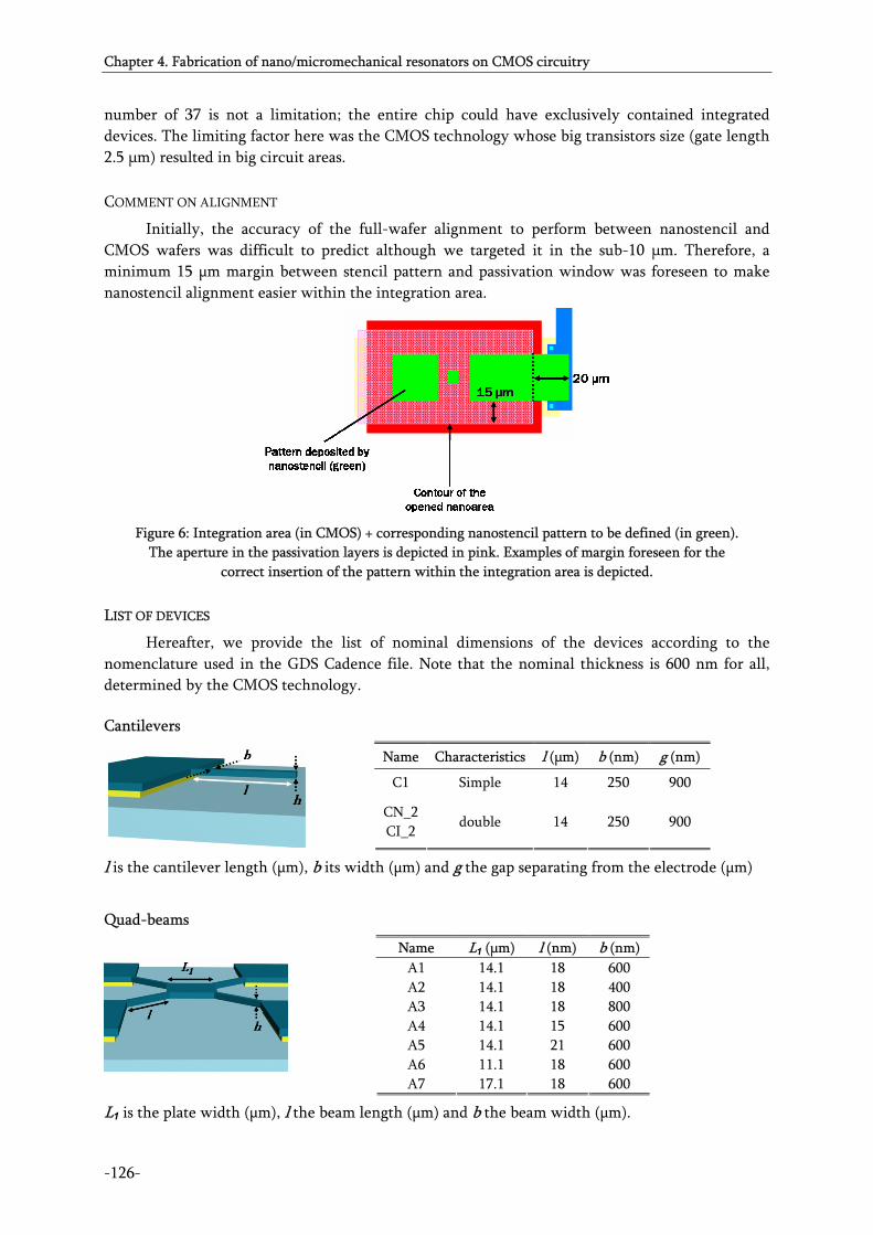
Chapter 4. Fabrication of nano/micromechanical resonators on CMOS circuitry
-126-
number of 37 is not a limitation; the entire chip could have exclusively contained integrated devices. The limiting factor here was the CMOS technology whose big transistors size (gate length 2.5 μm) resulted in big circuit areas.
COMMENT ON ALIGNMENT
Initially, the accuracy of the full-wafer alignment to perform between nanostencil and CMOS wafers was difficult to predict although we targeted it in the sub-10 μm. Therefore, a minimum 15 µm margin between stencil pattern and passivation window was foreseen to make nanostencil alignment easier within the integration area.
Figure 6: Integration area (in CMOS) + corresponding nanostencil pattern to be defined (in green).
The aperture in the passivation layers is depicted in pink. Examples of margin foreseen for the correct insertion of the pattern within the integration area is depicted.
LIST OF DEVICES
Hereafter, we provide the list of nominal dimensions of the devices according to the nomenclature used in the GDS Cadence file. Note that the nominal thickness is 600 nm for all, determined by the CMOS technology.
Cantilevers
Name Characteristics l (μm) b (nm) g (nm) C1 Simple 14 250 900
CN_2CI_2
double 14 250 900
l is the cantilever length (µm), b its width (µm) and g the gap separating from the electrode (µm)
Quad-beams
Name L1 (μm) l (nm) b (nm) A1 14.1 18 600 A2 14.1 18 400 A3 14.1 18 800 A4 14.1 15 600 A5 14.1 21 600 A6 11.1 18 600 A7 17.1 18 600
L1 is the plate width (µm), l the beam length (µm) and b the beam width (µm).

Chapter 4. Fabrication of nano/micromechanical resonators on CMOS circuitry
-127-
I.2. Electron beam lithography
Electron beam lithography (eBL) started its development in early 70s and since then, it has represented an alternative to conventional optical lithography (OL) for the definition of submicron patterns. Actually, eBL consists in irradiating by means of a focused electron beam a surface coated with an electron sensitive resist. eBL is a direct writing technique utilizing electrons as irradiation support, on the contrary to optical techniques that require an opaque mask and light respectively. Physically, enhanced resolution is obtained basically since electronic radiation is not limited by diffraction effects that affect the resolution of OL.
With such an eBL system, a layout is directly written through the spatial monitoring of a high energy electron beam applied upon a surface whose top material (a coated resist) properties are physically or chemically modified by the incident beam. The subsequent step is the development of the sample in order to remove the irradiated part of the resist (if it is positive).
The key parameters determining the efficiency of an eBL step [34] are the beam shape and its characteristics, its electronic energy, electron-matter interactions, resist thickness and molecular structure, the development solution and time, but also the design of the structure to be drawn. In recent years, every element of the system has known a big progress; more stable filaments are now available, beam diameter has been reduced down to few nm, and globally the whole eBL process (electron generation and focus, sample displacement, etc…) is fully automated.
At CNM, our eBL consists of a Scanning Electron Microscope (SEM) completed by a set of electronic devices that control beam deflection and blanking. The SEM system provides the electron source, focusing elements and a movable substrate holder for nano/micropositioning. PMMA (PolyMethilMethaCrylate) is used as a resist.
In industry and research areas, eBL is mainly applied to the fabrication of masks, for device prototyping and fabrication in low amounts. More generally, it is useful in research for very specific applications (nano/microelectrodes patterning, etc…). For us at CNM, the use of eBL is of interest for its high resolution and versatility. Indeed, it allows rapid fabrication of new prototypes, since it is a direct writing method that does not require purchasing a mask each time that first prototypes of a new device have to be produced. In this sense, it is cost and time effective. eBL is also capable of realizing patterns in a large range of dimensions (50 nm - 100 μm).
Nevertheless, intrinsically and comparatively with nSL, eBL suffers a series of limitations. First, the cost of the system is relatively high. Second, its slowness and low throughput must be pointed out. Compared to nSL, OL or NIL which are parallel, eBL is serial what considerably slows the patterning of a full wafer. In comparison with nSL, eBL requires more related process steps: resist coating, exposure, development, metallization and lift-off, in other words five steps, while nSL only requires one evaporation, i.e. one single step (two if counting alignment and clamping).
Third, the large quantity of parameters and the complexity of operation imply a low reproducibility of eBL systems. Constant technical support is required and only big foundries can afford having an entire team devoted to the optimization of the system.
Last but not least, some authors have pointed out the fact that eBL degrades the performance of the CMOS circuitry [35] when it is implemented as nanolithography technique for the fabrication of nanodevices on pre-fabricated CMOS substrates. In contrast, in section II.3.f, CMOS compatibility of nSL is discussed: in our samples, no relevant change between before and after post-processing has been observed.

Chapter 4. Fabrication of nano/micromechanical resonators on CMOS circuitry
-128-
II. Fabrication of micro/nanomechanical resonators on CMOS by nanostencil lithography (nSL)
This work is the result of an intensive collaboration realized with LMIS1 (Microsystems Laboratory 1) from EPFL (Lausanne, Switzerland) in the frame of the NaPa European project, in particular with Dr. Marc .A.F. van den Boogaart, who was pursuing his PhD at this time on Stencil Lithography, and Professor Jürgen Brugger. To less extent, SÜSS MICROTEC also participated in the development of tools for stencil/CMOS alignment, in particular a specific chuck was designed for adapting to a standard SÜSS MICROTEC bond aligner.
Figure 7 shows the time evolution of different tasks related to NaPa project and my thesis. Between the beginning of the project (in 2004) and the first demonstration of device functionality, about 20-22 months passed. It has been a success and further advancements are still in course.
TASKS CORRESPONDANCE
CMOS Nanostencil (nSL) Associated processes Applications of
NEMS/CMOS devices C1: CCII circuit design and simulations C2: circuit layout C3: circuit fabrication C4: circuit pre-test C5: tests of CMOS integrated cantilevers C6: tests of CMOS integrated quad-beams (QB)
N1: design (CNM) and fabrication (EPFL) of 1ST generation of chip-sized stencils N2: first tests with non-custom CMOS chips N3: design (CNM) and fabrication (EPFL) of full-wafer nanostencils
AP1: characterization of ‘blurring effect’ AP2: fabrication of dummy wafers for process tests PP: post-processing of CMOS wafers by nSL AP3 and AP4: development of release etchings of integrated cantilevers (AP3) and QB (AP4)
S1: implementation of NEMS/CMOS as highly sensitive mass sensors to monitor the deposition of ultra-thin gold layers S2: implementation of NEMS/CMOS as positioning sensors in quasi-dynamic stencil lithography system
Figure 7. Time evolution of my thesis work for NaPa project
Up to our knowledge, this work represents the first time that patterning of full CMOS wafers with nanostencil lithography is achieved and probably even the first time that a relatively low cost full wafer monolithic integration of nanodevices on CMOS has been demonstrated. Actually, advanced optical lithography can be used to define devices on CMOS at nanometer scale, but it requires the use of expensive equipment and materials, as well as complex processing only available for large microelectronics companies specialized in the fabrication of large series of semiconductor memories and microprocessors. Other emerging lithography techniques have

Chapter 4. Fabrication of nano/micromechanical resonators on CMOS circuitry
-129-
already been used to pattern devices on CMOS, like e-beam lithography [36], laser lithography [37] or nanoimprint lithography, but none of them had simultaneously demonstrated a reliable and CMOS compatible full wafer patterning.
By combining the technology for the fabrication of nanomechanical resonators with a standard CMOS technology, we present a novel wafer-scale (100 mm) technological process based on post-processing pre-fabricated CMOS circuits using nSL. This approach separates CMOS circuit fabrication and nanodevice fabrication, so that two different lithography techniques for each phase are used. Thus, a rather low-cost nanolithography technique may be implemented on CMOS substrates whose processing does not require an ultra-advanced patterning technique. In this context, nSL is adequate since it is clean (resistless), direct and parallel.
As it will be shown, we have succeeded in the parallel definition and fabrication of multiple (∼2000) silicon nanomechanical resonators at the 200 nm scale that are monolithically integrated into CMOS circuits. Further decreasing the resolution should be soon possible.
II.1. CNM CMOS technology
The CMOS circuit fabrication is based on CNM ‘in house’ process (www.cnm.es) (described in detail in annex A7.1). This technology includes two polysilicon layers and a single metal level. The minimum feature size of the channel length is limited to 2.5 μm. Two different polysilicon layers are employed for specific functions:
the so-called poly0 layer is implemented as a capacitor electrode material the so-called poly1 layer is implemented as transistor gate material
This is not a leading CMOS technology, but it allows a certain degree of flexibility on the process flow; in other words some parameters can be modified. In particular, it has been possible to change the initial deposition parameters of poly0 in order to improve its crystalline quality so that it may be used as structural layer of the resonator. It has been possible as well to choose its thickness for optimizing the resonator dimensions.
Taking into account the know-how acquired during previous projects, different aspects of the technology regarding the combination with NEMS fabrication have been optimized for reaching a much higher final fabrication yield.
The main modification, that is schemed in Figure 8, has consisted not in changing the process but in modifying the layout of given photolithography masks in order to obtain with high yield viable integration areas for posterior integration of nano/micromechanical resonators inside them. Basically, in the new CMOS circuit layout no aperture in the interlevel oxide is made on top of the integration areas so that this dielectric layer protects the underlying polysilicon layers during the subsequent metal etching. Indeed, the dry etching of metal is not uniform and from one point of the wafer to another the removal of metal is not realized at the same speed: while in some integration areas some metal still has to be etched, in others the process has already started overetching and damaging the two underlying layers: poly1 and thin SiO2.
Now, the structuring by dry etching of interlevel oxide within all integration areas is made immediately after the etching of the passivation layer with the same masking resist (photolithography reticule nº8 named passivation): a single mask level allows opening both layers with a prolonged reactive ion etching (RIE). In this way, the interlevel oxide protects the integration area during the whole process.

Chapter 4. Fabrication of nano/micromechanical resonators on CMOS circuitry
-130-
PREVIOUS PROCESS FLOW NEW PROCESS FLOW
(a). an aperture in the interlevel oxide is made on top of the integration area
(a’). no aperture in the interlevel oxide is made on top of the integration area
(b). at the end of the dry etching of Al (interconnections), the lack of etching homogeneity at wafer scale requires an over-etching that locally damages some integration areas until the point that the poly1 and the thin oxide are completely removed
(b’). the lack of homogeneity of the Al dry etching and the related necessary overetch do not damage the integration area as it is protected by the interlevel oxide (the Al dry etching is selective respect to SiO2 but not respect to polySi).
(c). passivation layer deposition and patterning
(c’). passivation layer deposition and patterning. The dry etching also removes the interlevel oxide within the integration area.
(d). during poly1 etching, poly0 is completely etched
(d’). poly1 etching is stopped at the bottom by the thin SiO2 layer and does not etch poly0
Figure 8. Previously and newly implemented CMOS process (partial) flows for posterior NEMS integration