12-w ultra-wide input range power supply - ti calculations listed in this section are for the...
TRANSCRIPT

Primary GROUND
15V 0.8A
SECONDARYGROUND
24 to 250-VDC88-276VAC
CBLK
VDC
Bridge Rectifier
EMI FilterEMC Filter
Booster PWM
Controller TPS40210
UVLO Circuit
LMS33460
QR Flyback PWM
Controller UCC28740
355VDC
VDC
VDRV
Isolated Feedback
Shunt Voltage Reference
TL431
VAUX
DC-DC Booster Inductor
DC-DC Booster MOSFET
DC-DC Booster Output Diode
Fly backTransformer,And Snubber
Fly backMOSFET
CurrentSense
Resistor
CurrentSense
Resistor
Flyback ConverterOutput Diode
LC Filter
Start Up Circuit LMS33460
Voltage Divider
15V
355VDC VAUX
Isolation Barrier
Voltage Divider
VFB VFBVAUX
TI Designs12-W Ultra-Wide Input Range Power Supply
TI Designs Design FeaturesTI Designs provide the foundation that you need The 12-W Ultra-Wide Input Range Power Supply is aincluding methodology, testing and design files to reference design that is primarily targeted forquickly evaluate and customize the system. TI Designs protection relays. This design is a single-boardhelp you accelerate your time to market. solution that handles an ultra-wide range of AC or DC
inputs.Design Resources • Supply Voltage Range
– 24-V to 250-V DC or 88-V to 276-V ACTool Folder Containing Design FilesTIDA-00227• Output Voltage at Nominal Supply VoltageTPS40210DGQR Product Folder
UCC28740 Product Folder – 15 V, 0.8 ALMS33460MG/NOPB Product Folder – Total Output Power 12 WTL431AIDBZ Product Folder – Line Regulation < ±3%
• 21-V to 250-V DC and 80-V to 276-V ACASK Our E2E Experts – Load Regulation < ±3%WEBENCH® Calculator Tools • (10 to 100%)
– Form Factor• PCB Dimension 100 × 100 mm
• Meets Pre-Compliance Test Requirements– IEC61000-4 for EFT and Surge– EN55011 Class A Conducted Emission– IEC61000-4-11 (AC) and IEC61000-4-29 (DC)
for Voltage Dips and Interruptions with ReducedBulk Capacitor
Featured Applications• Protection Relay: Single Function and Multifunction• Substation IED and Automation Products• Power Managers
All trademarks are the property of their respective owners.
1TIDU389–June 2013 12-W Ultra-Wide Input Range Power SupplySubmit Documentation Feedback
Copyright © 2013, Texas Instruments Incorporated

System Description www.ti.com
An IMPORTANT NOTICE at the end of this TI reference design addresses authorized use, intellectual property matters and otherimportant disclaimers and information.
1 System DescriptionProtection relays play a critical role in electrical grids, substations, and power distribution systems. Theserelays protect the electrical power system against different electrical faults. The heart of this protectionrelay design is a smart controlling unit that continuously monitors electrical parameters such as voltages,currents, and frequencies. This smart controlling unit also issues trip commands to appropriate circuitbreakers during faults.
There are different types of relays, depending upon the stage used. Types of protection relays include:generator protection, distance protection, overvoltage protection, overcurrent protection, and differentialprotection.
Protection relays are either self-powered or powered by auxiliary ports.
1.1 Power Supply Input Voltage
The input power supply can vary from 20-V DC to 250-V DC and 40-V AC to 250-V AC. The completerange of the operating input power supply voltage range is divided into multiple types.• Type 1: 20- to 65-V DC• Type 2: 37- to 150-V DC, 32 to 110 V AC• Type 3: 87- to 300-V DC, 80 to 265-V AC
NOTE: Categorization of input into number of types of input range is dependent on manufacturers.
The burden on the auxiliary supply depends on the features offered by the protection relay and can varyfrom 4 W to 12 W for many of the protection relays. Protection relays with enhanced communication andI/O features may consume > 12 W.
1.2 Power Supply Interruption (Critical Protection-Relay Requirement)One of the critical requirement when dealing with protection relays is to withstand the interruption of inputvoltage without restarting. The power supply interruption time depends on the power consumption of therelay and reduces with an increase in consumption.
To achieve the required backup time, larger capacitors are used. Electrolytic capacitors have reliabilityconcerns; therefore, higher values may not be preferred.
This TI design reduces the capacitance required for the power supply to comply IEC61000-4-11 (AC) andIEC61000-4-29 (DC) for voltage variations and interruption.
1.3 12-W Power SupplyThis design guide provides details to design a 12-W power supply used in protection relay. This 12-Wultra-wide range input-supply design serves as a ready-to-use reference design for protection relay. Thisdesign is a single-board power solution that handles an ultra-wide input range of AC or DC inputs. TI hasa large portfolio of power solutions that can be used to design this power supply.
See Section 7 for the required schematics, PCB, test reports, and design calculations to design the powersupply with reduced effort.
2 12-W Ultra-Wide Input Range Power Supply TIDU389–June 2013Submit Documentation Feedback
Copyright © 2013, Texas Instruments Incorporated

Primary GROUND
15V 0.8A
SECONDARYGROUND
24 to 250-VDC88-276VAC
CBLK
VDC
Bridge Rectifier
EMI FilterEMC Filter
Booster PWM
Controller TPS40210
UVLO Circuit
LMS33460
QR Flyback PWM
Controller UCC28740
355VDC
VDC
VDRV
Isolated Feedback
Shunt Voltage Reference
TL431
VAUX
DC-DC Booster Inductor
DC-DC Booster MOSFET
DC-DC Booster Output Diode
Fly backTransformer,And Snubber
Fly backMOSFET
CurrentSense
Resistor
CurrentSense
Resistor
Flyback ConverterOutput Diode
LC Filter
Start Up Circuit LMS33460
Voltage Divider
15V
355VDC VAUX
Isolation Barrier
Voltage Divider
VFB VFBVAUX
www.ti.com Design Features
2 Design FeaturesTypical power supply requirements are shown in Table 1.
Table 1. Power Supply Requirements
REQUIREMENTS REQUIREMENT PARAMETER PARAMETER VALUESOutput power in W 12Input voltage DC 24-V to 250-V DCInput voltage AC 88-V to 276-V AC
Functional requirement Output voltages and current 15 V, 0.8 ALoad regulation — 10 to 100% <±3%Line regulation — AC/DC inputs <±3%Output ripple <200-mV peak-to-peak at 15 VConducted Emission EN55011 Class AEFT IEC 61000-4-4, Level 4
Pre-compliance IEC 61000-4-5,Surge Level 3 - Differential Mode
Level 4 - Common ModeThe design should support 15 V at 0.8 APermissible power interruption to maintain <100 ms at 24-V DC during the interruption time specified withnormal operation 100% load.
3 Block DiagramThe 12-W power-supply design handles ultra-wide ranges of AC or DC inputs, making the power-supply asuitable platform for a variety of protection relays. The power supply provides excellent line and loadregulation. The design has been pre-compliance tested for IEC61000-4 (EFT and Surge) and EN55011Class A (Interference).
Figure 1. Block Diagram
3TIDU389–June 2013 12-W Ultra-Wide Input Range Power SupplySubmit Documentation Feedback
Copyright © 2013, Texas Instruments Incorporated
Block Diagram www.ti.com
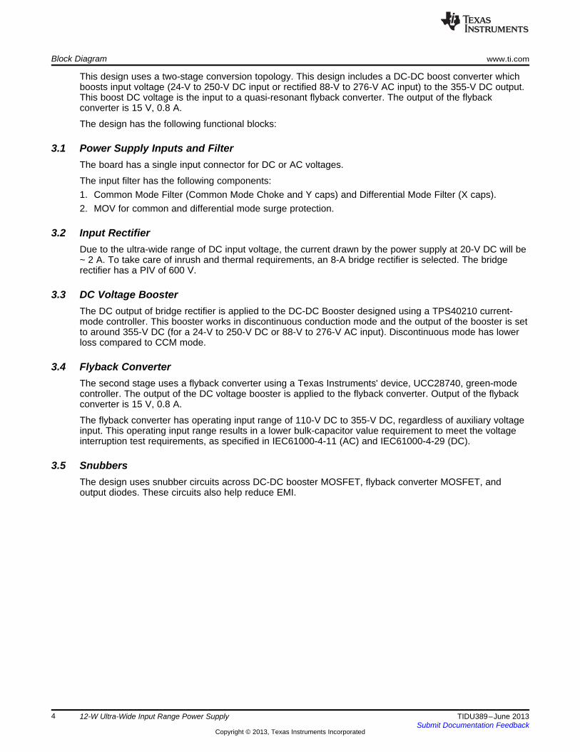
This design uses a two-stage conversion topology. This design includes a DC-DC boost converter whichboosts input voltage (24-V to 250-V DC input or rectified 88-V to 276-V AC input) to the 355-V DC output.This boost DC voltage is the input to a quasi-resonant flyback converter. The output of the flybackconverter is 15 V, 0.8 A.
The design has the following functional blocks:
3.1 Power Supply Inputs and FilterThe board has a single input connector for DC or AC voltages.
The input filter has the following components:1. Common Mode Filter (Common Mode Choke and Y caps) and Differential Mode Filter (X caps).2. MOV for common and differential mode surge protection.
3.2 Input RectifierDue to the ultra-wide range of DC input voltage, the current drawn by the power supply at 20-V DC will be~ 2 A. To take care of inrush and thermal requirements, an 8-A bridge rectifier is selected. The bridgerectifier has a PIV of 600 V.
3.3 DC Voltage BoosterThe DC output of bridge rectifier is applied to the DC-DC Booster designed using a TPS40210 current-mode controller. This booster works in discontinuous conduction mode and the output of the booster is setto around 355-V DC (for a 24-V to 250-V DC or 88-V to 276-V AC input). Discontinuous mode has lowerloss compared to CCM mode.
3.4 Flyback ConverterThe second stage uses a flyback converter using a Texas Instruments' device, UCC28740, green-modecontroller. The output of the DC voltage booster is applied to the flyback converter. Output of the flybackconverter is 15 V, 0.8 A.
The flyback converter has operating input range of 110-V DC to 355-V DC, regardless of auxiliary voltageinput. This operating input range results in a lower bulk-capacitor value requirement to meet the voltageinterruption test requirements, as specified in IEC61000-4-11 (AC) and IEC61000-4-29 (DC).
3.5 SnubbersThe design uses snubber circuits across DC-DC booster MOSFET, flyback converter MOSFET, andoutput diodes. These circuits also help reduce EMI.
4 12-W Ultra-Wide Input Range Power Supply TIDU389–June 2013Submit Documentation Feedback
Copyright © 2013, Texas Instruments Incorporated

www.ti.com Circuit Design and Component Selection
4 Circuit Design and Component SelectionFor more information on each of these devices, refer to the respective product folders at www.TI.com.
4.1 Front-End EMC FilterFor calculation of the EMC filter and other EMC considerations, see the following application notesavailable on the TI website:
• Designing Magnetic Components for Optimum Performance in Low-Cost AC/DC ConverterApplications (SLUP265).
• AN-2162 Simple Success With Conducted EMI From DC-DC Converters (SNVA489).• Understanding and Optimizing Electromagnetic Compatibility in Switchmode Power Supplies
(SLUP202).
4.2 DC-DC Booster DesignThe DC-DC booster is configured using the TPS40210 controller. The TPS40210 device is a wide-inputvoltage (4.5 V to 52 V), nonsynchronous boost controller.
The TPS40210 device is suitable for topologies that require a grounded source N-channel FET includingboost, flyback, SEPIC, and various LED driver applications. Current-mode control provides improvedtransient response and simplified loop compensation.
The following are features of the DC-DC booster:• Adjustable oscillator frequency• Fixed frequency current mode control• Internal slope compensation• Integrated low-side driver• Programmable, closed-loop soft start• Overcurrent protection• External synchronization capability• Reference 700 mV (TPS40210)• Low-current disable function
Figure 2. DC-DC Booster Design Using theTPS40210DGQ
5TIDU389–June 2013 12-W Ultra-Wide Input Range Power SupplySubmit Documentation Feedback
Copyright © 2013, Texas Instruments Incorporated
Circuit Design and Component Selection www.ti.com
4.2.1 Power Supply Design Parameters
1. Input voltage DC: 24-V to 250-V DC2. Input voltage AC: 88-V to 276-V AC3. Output voltage: 15 V, 0.8 A
4.2.2 DC-DC Booster Design CalculationThe calculations listed in this section are for the booster inductor, based on the TI application note,Inductor and Flyback Transformer Design (SLUP127).
4.2.2.1 Booster Design Parameters• Minimum DC input voltage, (V):
VINDC(MIN) = 18 V• Maximum DC input voltage, (V):
VINDCMAX = 250 V• Minimum AC input voltage, (V):
VINAC(MIN) = 80 V• Maximum AC input voltage, (V):
VINAC(MAX) = 276 V• Bridge rectifier drop, (V):
VBR = 0.7 V• Bus voltage, (V):
VBUS(MAX) = VINAC(MAX) × 1.4142 – 2 × VBR (1)VBUS(MIN) = VINDC(MIN) – 2 × VBR (2)VBUS(MAX) = 389-V DC (3)
The range of VBUS can be from 16.6-V DC to 389-V DC• Second stage output power:
PFLYBACKOUT = 12.5 W– Flyback output VFLYBACKOUT = 15 V– Flyback output diode drop = 0.7 V– Flyback output current 0.8 A
PFLYBACKOUT = ( VFLYBACKOUT + VD) × IFLYBACKOUT = (15 + 0.7) × 0.8 ~ 12.5 W (4)• Efficiency of second stage:
τ2 = (80%) 0.8• Output power of booster:
PBOOSTERIN = 16 W• Efficiency of booster:
τ1 = (80%) 0.8• Input power of booster:
PBOOSTERIN = 20 W• Output voltage of the booster:
VBOOSTOUT = 355 VBooster output is set at 355 V for 18- to 250-V DC or 88- to 250-V AC. Above 250-V AC, the boostfunction is disabled, and rectified voltage appears directly across the booster-output capacitor. Thebooster output is set to 355 V to take care of maximum duty-cycle limitation of TPS40210. At 276-VAC, the booster output will be around 390-V DC. For the calculation of booster parameters, 355-V DCis considered as booster output.
6 12-W Ultra-Wide Input Range Power Supply TIDU389–June 2013Submit Documentation Feedback
Copyright © 2013, Texas Instruments Incorporated

( ) ( )
( )(CRIT)
2OUT D IN IN
OUT 2OUT D SW
V V V VI
2 V V f L
+ - ´=
´ + ´ ´
MAX
MAX
1D 1 0.95
M= - =
BOOSTOUT MIN
BUSMAX
V 355M 0.91
V 389= = =
BOOSTOUT MAX
BUSMIN
V 355M 21.39
V 16.6= = =
BOOSTOUTBOOSTOUT
BOOSTOUT
VR 8066
I= = W
BOOSTEROUTBOOSTOUT
BOOSTOUT
P 20I 0.044 A
V 355 = = =
www.ti.com Circuit Design and Component Selection
• Output average current of the booster:
(5)• Output load of the booster:
(6)
4.2.2.2 Preliminary Calculation• Voltage gain of the booster:
(7)
(8)• Duty cycle:
(9)• Switching frequency, (Hz):
FSW = 35000• Time period, s:
TSW = 28.57 µs• Critical inductor value to keep in discontinuous mode:
LCRITICAL ≤ 0.5 × RBOOSTOUT × TSW × DMAX× (1 – DMAX) × (1 – DMAX) ≤ 240 µH (10)• Choose value of booster inductor:
LBOOSTER = 150 µH to avoid transition from DCM to CCM mode at lower voltage input range.Justification for using 150 µH inductor value is explained in the following paragraphs.As per the application information given in TPS40210, TPS40211 4.5-V to 52-V Input Current ModeBoost Controller (SLUS772).Converters using freewheeling diodes have a load-current level at which they transition fromdiscontinuous conduction to continuous conduction. This is the point where the inductor current justfalls to zero. At higher load currents, the inductor current does not fall to zero but remains flowing in apositive direction and assumes a trapezoidal wave shape as opposed to a triangular wave shape. Thisload boundary between discontinuous conduction and continuous conduction can be found for a set ofconverter parameters as in Equation 11.
where•• VOUT is the output voltage of the converter in V• VD is the forward conduction voltage drop across the rectifier or catch diode in V• VIN is the input voltage to the converter in V• IOUT is the output current of the converter in A• L is the inductor value in H• fSW is the switching frequency in Hz (11)
Based on Equation 11, the results in Table 2 and Table 3 are obtained for different values of inputvoltages for two different values of booster inductor.
7TIDU389–June 2013 12-W Ultra-Wide Input Range Power SupplySubmit Documentation Feedback
Copyright © 2013, Texas Instruments Incorporated

Circuit Design and Component Selection www.ti.com
Table 2. DCM to CCM Transition for 250 µH Inductor
VIN, V DCM/CCML, H VO, V VD, V Board VIN, V After Bridge fSW, Hz Boundary Mode
Rectifier Current0.00025 355 0.7 29.5 28 35000 0.1160.00025 355 0.7 28.5 27 35000 0.1080.00025 355 0.7 27.5 26 35000 0.1010.00025 355 0.7 26.5 25 35000 0.0930.00025 355 0.7 25.5 24 35000 0.0860.00025 355 0.7 24.5 23 35000 0.0790.00025 355 0.7 23.5 22 35000 0.0730.00025 355 0.7 22.5 21 35000 0.0670.00025 355 0.7 21.5 20 35000 0.0610.00025 355 0.7 20.5 19 35000 0.0550.00025 355 0.7 19.5 18 35000 0.0490.00025 355 0.7 18.5 17 35000 0.0440.00025 355 0.7 17.5 16 35000 0.039
Table 2 indicates that at lower input voltage of 19.5 V, the booster crosses from DCM to CCM mode ata load current of 0.049 A; thus, resulting in a state of instability.With 150-µH Inductor, DCM to CCM mode current is always more than the booster output currentIo = 0.045 A required at 18-V DC, so no state of instability is reached as shown in Table 3.
Table 3. DCM to CCM Transition for 150 µH Inductor
VIN, V DCM/CCML, H VO, V VD, V Board VIN, V After Bridge fSW, Hz Boundary Mode
Rectifier Current0.00015 355 0.7 29.5 28 35000 0.1930.00015 355 0.7 28.5 27 35000 0.180.00015 355 0.7 27.5 26 35000 0.1680.00015 355 0.7 26.5 25 35000 0.1560.00015 355 0.7 25.5 24 35000 0.1440.00015 355 0.7 24.5 23 35000 0.1320.00015 355 0.7 23.5 22 35000 0.1220.00015 355 0.7 22.5 21 35000 0.1110.00015 355 0.7 21.5 20 35000 0.1010.00015 355 0.7 20.5 19 35000 0.0910.00015 355 0.7 19.5 18 35000 0.0820.00015 355 0.7 18.5 17 35000 0.0740.00015 355 0.7 17.5 16 35000 0.065
8 12-W Ultra-Wide Input Range Power Supply TIDU389–June 2013Submit Documentation Feedback
Copyright © 2013, Texas Instruments Incorporated

2 2
AC RMS DCI I I 0.89 A= - =
( ) ( ) ( ) RMS MAX LPEAK MIN LPEAK MIN LPEAK MINI [D I I I I I I ] 1.69 A= ´ ´ + - ´ - =
BUSMINLPEAK SW MAX
BOOSTER
VI T D 3.01 A
L= ´ ´ =
www.ti.com Circuit Design and Component Selection
• Inductor peak current, (A):
(12)• Inductor minimum current, (A):
IMIN = 0 A• Average value of trapezoidal waveform, (A):
IPA= 0.5 × (ILPEAK + IMIN) = 1.51 A (13)• DC value of trapezoidal waveform, (A):
IDC = DMAX × IPA = 1.44 A (14)• RMS value of trapezoidal waveform, (A):
(15)• AC value of trapezoidal waveform, (A):
(16)• Maximum-peak short-circuit current:
ISCPK = I LPEAK × 1.2 = 3.62 A (17)
An inductor of 150 µH with rated current shown in Equation 17 is required.
4.2.2.3 Switching FrequencySwitching frequency of the DC-DC converter is chosen to be 35 KHz so as to get enough ON time athigher line voltages. RT and CT values are chosen to be 1.33 M and 470 pF.
Figure 3. Frequency versus Timing Resistance for TPS40210
9TIDU389–June 2013 12-W Ultra-Wide Input Range Power SupplySubmit Documentation Feedback
Copyright © 2013, Texas Instruments Incorporated

( )
( )BOOSTOUTRIPPLE
OUT LPEAK BOOSTOUT
7 VESR C 0.083
(8 I I-
´= = W
´
( )BOOSTOUT MAXOUT
BOOSTOUT RIPPLE SW)
8 I DC
(V F
´ ´=
´
Circuit Design and Component Selection www.ti.com
4.2.2.4 Output Diode Selection• Considering 80% dating on VOUT for ringing on the switch node. The rectifier diode minimum reverse
breakdown voltage is given by:VPIVBDIODE ≥ 1.25 × VBOOSTOUT ≥ 450 V (18)
• The diode must have a reverse breakdown voltage greater than 500 V. The rectifier diode peak andaverage currents are estimated by:IBD(AVG) = IBOOSTOUT = 0.045 AIBD(PEAK) = ILPEAK = 3.01 A
• The power dissipation in the diode is estimated by:PBDiode = IBD(AVG) × VF = 0.03 W (19)
Table 4. Diode Specifications
SELECTED DIODEPart Number STTH8L06Type of Diode UltrafastPIV 600 VIF 8 ASurge Non-repetitive Forward Current 120 A
4.2.2.5 Output Capacitor Selection
where• VBOOSTOUTRIPPLE = 0.5 V• COUT with 20% tolerance = 23 µF (20)
(21)
Table 5. Output Capacitor Selection
Selected 33 µF 450 VCOUT
10 12-W Ultra-Wide Input Range Power Supply TIDU389–June 2013Submit Documentation Feedback
Copyright © 2013, Texas Instruments Incorporated

OUT
SS OUTEXTOUT 0C
Vt C
I I! u
SSSS
BP SS OFSTSS
BP FBSS OFST
tC
V VR In
V V V
ª º§ ·« »¨ ¸u« »¨ ¸ ¨ ¸« »© ¹¬ ¼
SW BOOSTER ISNS OCISNS
BOOSTER SW OUT D INOUT OC
F L VR
(2 L F I V V V
u u
u u u u
www.ti.com Circuit Design and Component Selection
4.2.2.6 Current Sense and Current Limit• The load current overcurrent threshold is set by the proper choice of RISNS. If the converter is operating
in discontinuous mode, the current sense resistor is as follows:
where• VISNS(OC) = 0.15 V• RISNS is approximately 20 mΩ (22)
• Power Dissipation in the current sense resistor:PISNS = I2
RMS × RISNS × DMAX ~ 1 W (23)
4.2.2.7 Soft Start CapacitorThe capacitor on the SS pin CSS also plays a role in overcurrent functionality. The design uses thecapacitor as the timer between restart attempts. The soft-start time must be long enough so that theconverter can start without entering an overcurrent state. Because the overcurrent state is triggered bysensing the peak voltage on the ISNS pin, the peak voltage must be kept below the overcurrent thresholdvoltage. The voltage on the ISNS pin is a function of the load current of the converter, the rate of rise ofthe output voltage and output capacitance, and the current sensing resistor. The total output current thatmust be supported by the converter is the sum of the charging current required by the output capacitorplus any external load that must be supplied during start up.
The soft start capacitor is selected based on following equations:
where• IC(Chg) is the output capacitor charging current in A• COUT is the total output capacitance in F• VOUT is the output voltage in V• tSS is the soft start time• IOUT(OC) is the desired overcurrent trip point in A• IEXT is any external load current in A• RSS(chg) is the SS charging resistance in Ω, typically 500 kΩ• CSS is the value of the capacitor on the SS pin, in F• VBP is the value of the voltage on BP pin, in V• VSS(ofst) is the approximate level shift from the SS pin to the error amplifier (approximately 700 mV)• VFB is the error amplifier reference voltage, 700 mV typical• Considering IEXT = 0.044 A and IOUT(OC) = 0.053 A, tSS is 1.33 seconds and CSS = 22 µF (24)
11TIDU389–June 2013 12-W Ultra-Wide Input Range Power SupplySubmit Documentation Feedback
Copyright © 2013, Texas Instruments Incorporated

Circuit Design and Component Selection www.ti.com
4.2.2.8 Duty Cycle ClampThe TPS40210 has a minimum off time of approximately 200 ns and a minimum on time of 300 ns. Thesetwo constraints place limitations on the operating frequency that can be used for a given input-to-outputconversion ratio. To keep these limits in check, a duty cycle clamp is used at an input voltage value lessthan 24 V. This is achieved by clamping the compensation pin voltage of TPS40210. The value is clampedto a voltage that is the sum of voltages obtained at R13 and R15 across pin 9 of TPS40210 and thevoltage drop across the Diode (D3) that is connected between the resistive divider and the compensationpin.
Figure 4. Duty Cycle Limiting Circuit
12 12-W Ultra-Wide Input Range Power Supply TIDU389–June 2013Submit Documentation Feedback
Copyright © 2013, Texas Instruments Incorporated

www.ti.com Circuit Design and Component Selection
4.3 Flyback Converter Design Using UCC28740The downstream converter is designed to work in quasi-resonant flyback mode with the followingspecification at the end of power supply stream.• Working input voltage range: 110-V to 390-V DC• Output voltage and power:
– 15 V, 0.8 A– Total power 12 W
The design uses a quasi-resonant mode topology. Quasi-resonant topology has reduced EMI, lowerswitching losses for higher power outputs, compared to a conventional hard-switched converter with fixedswitching frequency.
The UCC28740 isolated-flyback power-supply controller provides constant voltage (CV) using an opto-coupler to improve transient response for large-load variations. Constant-current (CC) regulation isaccomplished through primary-side regulation (PSR) techniques. This device processes information fromopto-coupled feedback and an auxiliary flyback winding for precise high-performance control of outputvoltage and current.
An internal 700-V startup switch, dynamically-controlled operating states, and a tailored modulation profilesupport ultra-low standby power without sacrificing startup time or output transient response.
Control algorithms in the UCC28740 allow operating efficiencies to meet or exceed applicable standards.The drive output interfaces to a MOSFET power switch. Discontinuous conduction mode (DCM) withvalley switching reduces switching losses. Modulation of switching frequency and primary current peakamplitude (FM and AM) keeps the conversion efficiency high across the entire load and line ranges.
The controller has a maximum switching frequency of 100 kHz and always maintains control of the peak-primary current in the transformer. Protection features keep primary and secondary component stresses incheck. A minimum switching frequency of 170 Hz facilitates the achievement of less than 10-mW no-loadpower.
UCC28740 Features• Less than 10-mW no-load power capability• Opto-coupled feedback for CV, and primary-side Regulation (PSR) for CC• Enables ±1% voltage regulation and ±5% current• Regulation across line and load• 700-V Startup switch• 100-kHz Maximum switching frequency enables• High-power-density charger designs• Resonant-ring valley-switching operation for highest overall efficiency• Frequency dithering to ease EMI compliance• Clamped gate-drive output for MOSFET• Overvoltage, low-line, and overcurrent protection functions• SOIC-7 package
13TIDU389–June 2013 12-W Ultra-Wide Input Range Power SupplySubmit Documentation Feedback
Copyright © 2013, Texas Instruments Incorporated

INDCMAXPS
DBLOCKING 01 D
INDCMAXPS
DBLOCKING 01 D
VN
(V (V V ))
VN 6
V (V V )
=
- +
= =
- +
Circuit Design and Component Selection www.ti.com
Figure 5. Typical Application Using UCC28710
4.3.1 Magnetics Calculation for Booster InductorThe following calculations are based on Exposing the Inner Behavior of a Quasi-Resonant FlybackConverter (SLUP302).
4.3.2 Flyback Design Parameters• DC input voltage, V VINDCMIN: 110• DC input voltage, V VINDCMAX: 390• Output voltage-01, V V01 = 15.0• Output current, A I01: 0.8• Output diode voltage drop, VD = 0.7• Total output load, PSLOAD = (V01 + VD) × I01 = 12.5 W• Efficiency of flyback converter, τ = 0.8• Primary input power = 15.6 W• Turn ratio calculation
(25)• Considering the blocking voltage of the output diode, VDBLOCKING = 60 V
14 12-W Ultra-Wide Input Range Power Supply TIDU389–June 2013Submit Documentation Feedback
Copyright © 2013, Texas Instruments Incorporated

VDS
VSEC
t t
t
ON RES
SW
tDEM AG
VBULK
V + VOUT F
t
t
ON
DEMAG
INDCMIN ON PS 01 D DEMAG
DEMAG SW ON RES
PS O1 D SW RESON
DCINMIN PS O1 D
V t N (V V ) t
t T t t
N (V V ) (T t )t
(V N (V V )
´ = ´ + ´
= - -
´ + ´ -
=
+ ´ +
www.ti.com Circuit Design and Component Selection
4.3.3 Primary Inductance CalculationFigure 6 represents the volt-second product during the on-time and the volt-second product during thedemagnetizing time. During every switching cycle, the flyback transformer maintains energy balance.Equating the on-time energy with the demagnetizing energy (with respect to the primary side) and thensubstituting for tDEMAG allows the calculation of tON.
(26)
The resonance created by the primary inductance and parasitic capacitance must last for a long-enoughtime so that the waveform can ring down to a level that the controller can interpret as indication thatanother switching cycle can begin. This time, tRES is equal to at least one-half of the resonant period, whichis the time to transition from peak to valley. The switching period is equal to the inverse of fSW and mustconsist of the on-time, tON, the demagnetizing time, tDEMAG and tRES.
TSW = tON + tDEMAG + tRES (27)
Figure 6. Volt Seconds During the On-Time Must Equal the Volt Seconds Duringthe Demagnetizing Time for Energy Balance
Assuming fRES will be less than 500 KHz so an initial assumption of tRES = 1 µs is a valid starting point.
tRES = 1 µS
By putting the values into Equation 27 we get tON.
tON = 6.5 µS
After calculating the initial on-time it is necessary to calculate the primary inductance, LPRIMARY which willsatisfy the energy requirement of the load at the switching frequency set for the minimum input voltage.
LPRIMARY = τ × (VINDCMIN × tON)2 × fSW / (2 × POUT) = 1094 µH (28)
15TIDU389–June 2013 12-W Ultra-Wide Input Range Power SupplySubmit Documentation Feedback
Copyright © 2013, Texas Instruments Incorporated

1/2
PRIMARY
P
L
S
LN 84T
A
84N 14T
6
æ ö= =ç ÷
ç ÷è ø
= =
OUTPRIPEAK
PRIMARY SW
2 PI ( ) 0.63 A
L f
´
= =
t´ ´
Circuit Design and Component Selection www.ti.com
By putting the respective parameter values in Equation 28 for LPRIMARY, we get:
LPRIMARY = 1094 µH
(29)
Initial calculations result in a primary inductance LPRIMARY = 1094 µH and a peak primary current of 0.63 A.
If initial calculations for tON and IPRIPEAK fall outside the dynamic modulations range of the controller thevalue for LPRIMARY must be iterated so that regulation is achieved over the frequency range enveloped bythe minimum and maximum frequency clamps — all while satisfying the maximum on-time IPRIPEAK andpower limit for the specified input voltage range and output power.
The UCC28740 design calculator (SLUC487) tool facilitates the iterative calculations.
After iterating to meet the controller requirements the final results are obtained which closely matches withthe calculator results.
LPRIMARY = 856 µH IPRIPEAK = 0.74 A ISCPEAK = 4.5 A (30)
4.3.4 Core SelectionTo keep the PCB size smaller, EE20/10/6 (EF20) Core is used. This core delivers up to 20-W power at 66KHz as indicated in Figure 7.
Figure 7. Power Level versus Operating Frequency for Selected Core
Given that LPRIMARY = 856 µH and from iteration AL value is set for 120 nH for one gapped core and oneun-gapped core.
(31)
4.3.5 Selected CoreEE20/10/6 (EF20) from Wurth is the selected core for the transformer design. TP4A is the core material.
Table 6. Effective Core Parameters
SYMBOL PARAMETER VALUE UNITVe Effective volume 1472 –mm3
Le Effective length 46 –mmAe Effective area 32 –mm2
16 12-W Ultra-Wide Input Range Power Supply TIDU389–June 2013Submit Documentation Feedback
Copyright © 2013, Texas Instruments Incorporated

8 3INDCMIN ONMAXac
e P
PRIMARY PRIPEAK 8
max
e P
V T10 2.66 10 Gauss 0.266 T 266 mT
A N
L I10 0.235 T 235 mT
A N
´b = ´ = ´ = =
´
´b = ´ = =
´
www.ti.com Circuit Design and Component Selection
4.3.6 Flux Density (AC) Calculations
(32)
For a flyback converter running in a discontinuous mode the AC flux density βac is equal to the maximumflux density βmax.
βmax is considered to be 270 mT max approximately.
Figure 8. B-H Curve for Selected Core
Saturation point for this core is about 400 mT, so this design is about 67% of maximum value.
4.3.7 Determine Core LossBunipolar = βac / 2 = 135 mT (33)
As indicated in Figure 8 for approximately for 66 KHz curve Pcore = 70 kW/m3
Ve per m3 = Ve / 10003 = 1.472 x 10⁻⁶ m3 (34)Pcore Loss = Pcore x Ve per m3 = 70 x 103 x 1.472 x 10-6 m3= 103 mW (35)
Figure 9. 4 Core Loss vs Flux Density for Selected Core at Different Operating Frequency
17TIDU389–June 2013 12-W Ultra-Wide Input Range Power SupplySubmit Documentation Feedback
Copyright © 2013, Texas Instruments Incorporated

PPEAKMOSFETLKG Primary
MAX SW
IV Leakage Inductance
DUTYCYCLE T u
u
INDCMAXSECONDARY DIODE 0
S
VPIV V
TURN RATIO
Circuit Design and Component Selection www.ti.com
4.3.8 PIV Rating for Secondary’s Diode
(36)• With values calculated above PIV for diodes comes to:
– PIV is 80 V for the secondary diodes– Secondary peak current: 4.5 A
4.3.9 Primary MOSFET Selection• Stress on MOSFET due to reflected voltage
VMOSFETREF = VDCINMAX + VOUT × TurnRatioS = ~ 477 V (37)• Stress due to leakage inductance
(38)• Considering leakage inductance to be < 5% of primary inductance value
– VMOSFETLKG = 112.2VMOSFETSTRESS = VMOSFETREF + VMOSFETLKG VMOSFETSTRESS = 502.2 V (39)
• Peak current IPEAKMOSFET = IPEAK = 0.74 A
All other component calculations are based on TI design sheet, UCC28740 Design Calculator Tool(SLUC487).
Table 7 shows the calculator with actual values entered.
Table 7. Values Entered in to UCC28740 Design Calculator
DESIGN REQUIREMENTS
Input SpecificationsInput Voltage Type, AC or DC AC Choose either AC or DCMinimum Input Voltage, VINPUTmin = 88 VACMaximum Input Voltage, VINPUTmax = 276 VACNominal Input Voltage, VINPUTnom = 250 VACMinimum Line Frequency, fLINEmin = 50 Hz enter 0 if DC input typeMinimum Input Voltage for Start-up, VINPUTrun = 80 VAC
Output SpecificationsRegulated Output Voltage, Constant Voltage Mode, 15 VDCVOUT_CV =Full Load Output Current, Constant Current Mode, IOCC = 0.8 ATarget Minimum Output Voltage During Constant Current 2 VDCRegulation, VOUT_CC =Allowable Output Voltage Drop During Load-Step 0.7 VTransient in Constant Voltage Mode, VOUTΔ =Maximum Peak-to-Peak Output Voltage Ripple, VRIPPLE = 150 mVMaximum Desired Switching Frequency, fMAX = 66 kHZOutput Over-Voltage Protection, VOUT_OVP = 16 VRequired Positive Load-Step Transient Current, ITRAN = 0.5 AMaximum Allowable Response Time to Load-Step 20 msTransient, tRESP =Maximum Stand-By Power Dissipation, PSB = 20 mW
Flyback Transformer, TRecommended Primary to Secondary Turns Ratio, NPS = 6.190 Recommended NPS
Enter ActualNPSActual Primary to Secondary Turns Ratio Used, NPS = 6.000Transformer Used
18 12-W Ultra-Wide Input Range Power Supply TIDU389–June 2013Submit Documentation Feedback
Copyright © 2013, Texas Instruments Incorporated
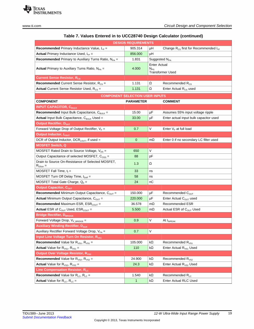
www.ti.com Circuit Design and Component Selection
Table 7. Values Entered in to UCC28740 Design Calculator (continued)DESIGN REQUIREMENTS
Recommended Primary Inductance Value, LP = 905.314 µH Change RCS first for Recommended LP
Actual Primary Inductance Used, LP = 856.000 µHRecommended Primary to Auxiliary Turns Ratio, NPA = 1.831 Suggested NPA
Enter ActualActual Primary to Auxiliary Turns Ratio, NPA = 4.000 NPS
Transformer UsedCurrent Sense Resistor, RCS
Recommended Current Sense Resistor, RCS = 1.131 Ω Recommended RCS
Actual Current Sense Resistor Used, RCS = 1.131 Ω Enter Actual RCS used
COMPONENT SELECTION USER INPUTSCOMPONENT PARAMETER COMMENTINPUT CAPACITOR, CBULK
Recommended Input Bulk Capacitance, CBULK = 15.00 µF Assumes 55% input voltage rippleActual Input Bulk Capacitance, CBULK Used = 33.00 µF Enter actual input bulk capacitor usedOutput Rectifier, DOUT
Forward Voltage Drop of Output Rectifier, VF = 0.7 V Enter VF at full loadOutput Inductor, LOUT
DCR of Output Inductor, DCRLOUT, if used = 0 mΩ Enter 0 if no secondary LC filter usedMOSFET Switch, QMOSFET Rated Drain to Source Voltage, VDS = 650 VOutput Capacitance of selected MOSFET, COSS = 88 pFDrain to Source On-Resistance of Selected MOSFET, 1.3 ΩRDSon =MOSFET Fall Time, tf = 33 nsMOSFET Turn Off Delay Time, tDoff = 58 nsMOSFET Total Gate Charge, Q0 = 24 nCOutput Capacitor, COUT
Recommended Minimum Output Capacitance, COUT = 150.000 µF Recommended COUT
Actual Minimum Output Capacitance, COUT = 220.000 µF Enter Actual COUT usedRecommended Maximum ESR, ESRCOUT = 36.578 mΩ Recommended ESRActual ESR of COUT Used, ESRCOUT = 5.500 mΩ Actual ESR of COUT UsedBridge Rectifier, DBRIDGE
Forward Voltage Drop, VF_BRIDGE = 0.9 V At IINPEAK
Auxiliary Winding Rectifier, DAUX
Auxiliary Rectifier Forward Voltage Drop, VFA = 0.7 VInput Line Voltage Turn On Resistor, RVS1
Recommended Value for RVS1, RVS1 = 105.000 kΩ Recommended RVS1
Actual Value for RVS1, RVS1 = 110 kΩ Enter Actual RVS1 UsedOutput Over Voltage Resistor, RVS2
Recommended Value for RVS2, RVS2 = 24.900 kΩ Recommended RVS2
Actual Value for RVS2, RVS2 = 24.3 kΩ Enter Actual RVS2 UsedLine Compensation Resistor, RLC
Recommended Value for RLC, RLC = 1.540 kΩ Recommended RLC
Actual Value for RLC, RLC = 1 kΩ Enter Actual RLC Used
19TIDU389–June 2013 12-W Ultra-Wide Input Range Power SupplySubmit Documentation Feedback
Copyright © 2013, Texas Instruments Incorporated
Test Setup www.ti.com
5 Test Setup
5.1 Equipment Used
1. Programmable DC voltage source 0 to 600 V, 0 to 5.5 A, Model TDK Lamda GEN600-5.52. Programmable AC voltage source 0 to 275 V, 5 A, Model California Instruments 1251P3. Single-phase AC power analyzer Voltech PM1004. Digital multimeter — 4-1/2 or better5. Electronic loads, Model KIKUSUI PLZ164WA
5.2 Procedure
1. Connect the required AC or DC source to the input terminals of the PSU. Reference designator – J1.2. Connect outputs to electronic loads. Reference designator – J2.3. Turn on the source with no load.4. Increase the load on 15 V output to approximately 0.8 A.
20 12-W Ultra-Wide Input Range Power Supply TIDU389–June 2013Submit Documentation Feedback
Copyright © 2013, Texas Instruments Incorporated
www.ti.com Test Results
6 Test Results
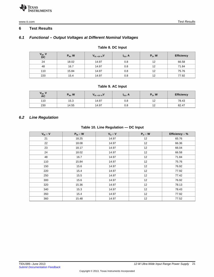
6.1 Functional – Output Voltages at Different Nominal Voltages
Table 8. DC Input
VIN, V PIN, W V01 +15 V,V IO1, A PO, W EfficiencyDC24 18.02 14.97 0.8 12 66.5848 16.7 14.97 0.8 12 71.84110 15.84 14.97 0.8 12 75.76220 15.4 14.97 0.8 12 77.92
Table 9. AC Input
VIN, V PIN, W V01 +15 V,V IO1, A PO, W EfficiencyAC110 15.3 14.97 0.8 12 78.43230 14.55 14.97 0.8 12 82.47
6.2 Line Regulation
Table 10. Line Regulation — DC Input
VIN – V PIN – W VO – V PO – W Efficiency – %21 18.25 14.97 12 65.7622 18.08 14.97 12 66.3623 18.17 14.97 12 66.0424 18.02 14.97 12 66.5848 16.7 14.97 12 71.84110 15.84 14.97 12 75.76150 15.6 14.97 12 76.92220 15.4 14.97 12 77.92250 15.5 14.97 12 77.42300 15.6 14.97 12 76.92320 15.36 14.97 12 78.13340 15.3 14.97 12 78.43350 15.4 14.97 12 77.92360 15.48 14.97 12 77.52
21TIDU389–June 2013 12-W Ultra-Wide Input Range Power SupplySubmit Documentation Feedback
Copyright © 2013, Texas Instruments Incorporated

Load (W)
Out
put (
V)
13.2 12 10.8 9.6 8.4 7.2 6 4.8 3.6 2.4 1.2 00
2
4
6
8
10
12
14
16
D003
AC Input (V)
Out
put (
V)
50 80 110 140 170 200 230 260 2900
2
4
6
8
10
12
14
16
D002AC Input (V)
Effc
ienc
y (%
)
50 80 110 140 170 200 230 260 29070
72
74
76
78
80
82
84
86
D001
Test Results www.ti.com
Table 11. Line Regulation — AC Input
VIN – V PIN – W VO – V PO – W Efficiency – %80 15.79 14.97 12 76110 15.3 14.97 12 78.43150 14.93 14.97 12 80.38175 14.74 14.97 12 81.41230 14.55 14.97 12 82.47240 14.47 14.97 12 82.93250 14.46 14.97 12 82.99260 14.26 14.97 12 84.15270 14.24 14.97 12 84.27
Figure 10. Output Voltage vs AC Input Voltage Figure 11. Efficiency vs AC Input Voltage
Figure 12. Load Regulation — 230-V AC Input
22 12-W Ultra-Wide Input Range Power Supply TIDU389–June 2013Submit Documentation Feedback
Copyright © 2013, Texas Instruments Incorporated

Load (W)
Out
put (
V)
13.2 12 10.8 9.6 8.4 7.2 6 4.8 3.6 2.4 1.2 00
2
4
6
8
10
12
14
16
D003
DC Input (V)
Effi
cien
cy (
%)
58
60
62
64
66
68
70
72
74
76
78
80
18 19 20 21 22 23 24 48 110 150 220 250 300 320 340 350 360
D004D001DC Input (V)
Out
put (
V)
0
1
2
3
4
5
6
7
8
9
10
11
12
13
14
15
16
17
18
18 19 20 21 22 23 24 48 110 150 220 250 300 320 340 350 360
D005
www.ti.com Test Results
Figure 13. Efficiency vs DC Input Voltage Figure 14. Line Regulation at DC Input Voltage
Figure 15. Load Regulation — 24-V DC Input
23TIDU389–June 2013 12-W Ultra-Wide Input Range Power SupplySubmit Documentation Feedback
Copyright © 2013, Texas Instruments Incorporated

Test Results www.ti.com
6.3 Load RegulationLoad is varied from 100% to 10% for all the loads together.
Table 12. Load Regulation PO 100% to 10% at 24-V DC Input
VIN – V PIN – W VO – V PO – W24 18 14.97 1224 15.91 14.97 10.824 14.14 14.97 9.624 12.31 14.97 8.424 10.61 14.97 7.224 8.9 14.97 624 7.2 14.97 4.824 5.45 14.97 3.624 3.84 14.97 2.424 2.09 14.97 1.2
Table 13. Load Regulation PO 10% to 100% at 230-V AC Input
VIN – V PIN – W VO – V PO – W230 14.55 14.97 12230 12.95 14.97 10.8230 11.55 14.97 9.6230 10.08 14.97 8.4230 8.71 14.97 7.2230 7.28 14.97 6230 5.91 14.97 4.8230 4.56 14.97 3.6230 3.12 14.97 2.4230 1.67 14.97 1.2
24 12-W Ultra-Wide Input Range Power Supply TIDU389–June 2013Submit Documentation Feedback
Copyright © 2013, Texas Instruments Incorporated

www.ti.com Test Results
6.4 Waveforms at Various Test Points as indicated
Figure 16. Start Up at 24-V DC, Full Load Figure 17. Start Up at 24-V DC, No Load
Figure 18. Booster Output VBOOST and Booster FET Drain Figure 19. Booster Output VBOOST and Booster FET DrainVoltage at 24-V DC Input Voltage at 110-V DC Input
Figure 20. Booster Output VBOOST and Booster FET Drain Figure 21. Booster Output VBOOST and Booster FET DrainVoltage at 340-V DC Input Voltage at 340-V DC Input
25TIDU389–June 2013 12-W Ultra-Wide Input Range Power SupplySubmit Documentation Feedback
Copyright © 2013, Texas Instruments Incorporated

Test Results www.ti.com
Figure 22. Booster Diode PIV at 88-V AC Figure 23. Booster Diode PIV at 220-V AC
Figure 24. Booster Output VBOOST and Flyback MOSFET Figure 25. Booster Output VBOOST and Flyback MOSFETDrain at 24-V DC Drain at 360-V DC
Figure 26. Booster Output VBOOST and Flyback MOSFET Figure 27. Booster Output VBOOST and Flyback MOSFETDrain at 80-V AC Drain at 270-V AC
26 12-W Ultra-Wide Input Range Power Supply TIDU389–June 2013Submit Documentation Feedback
Copyright © 2013, Texas Instruments Incorporated
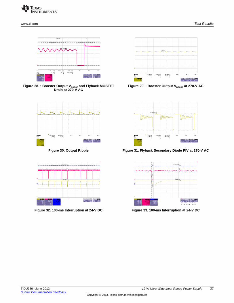
www.ti.com Test Results
Figure 28. : Booster Output VBOOST and Flyback MOSFET Figure 29. : Booster Output VBOOST at 270-V ACDrain at 270-V AC
Figure 30. Output Ripple Figure 31. Flyback Secondary Diode PIV at 270-V AC
Figure 32. 100-ms Interruption at 24-V DC Figure 33. 100-ms Interruption at 24-V DC
27TIDU389–June 2013 12-W Ultra-Wide Input Range Power SupplySubmit Documentation Feedback
Copyright © 2013, Texas Instruments Incorporated

Test Results www.ti.com
6.5 EMIThis design is tested for the following EMI pre-compliance testing.
Figure 34. Test Result with Average-Mode Measurement — Tested at 230-V AC
Figure 35. Test Result with Peak-Mode Measurement — Tested at 230-V AC
28 12-W Ultra-Wide Input Range Power Supply TIDU389–June 2013Submit Documentation Feedback
Copyright © 2013, Texas Instruments Incorporated

www.ti.com Test Results
6.6 EMCThis design is tested for following EMC pre-compliance testing.
Table 14. EMC (Tested at 230-V AC)
TEST APPLICABLE STANDARD TEST LEVEL OBSERVATIONEFT Test IEC 61000-4-4 Level 4 kV on power port Pass, Criteria B
a. 2-kV differential modeSurge Test IEC 61000-4-5 Pass, Criteria Bb. 4-kV common mode
6.7 Summary of Results
Table 15. Summary of Results
TEST PARAMETER TEST RESULT (OBSERVATION)20- to 250-V DC <1%
Line Regulation80- to 276-V AC <1%20- to 250-V DC 65 to 77%
Efficiency80- to 276-V AC 76 to 84%
Load Regulation 10 to 100% load variation <1%Ripple <100 mV peak to peak
Dip in the output voltage <5% for time Supports <100 ms interruption at 24-V DCPower Interruption Test ≥100 ms after auxiliary input voltage dips as per IEC61000-4-29to zero
29TIDU389–June 2013 12-W Ultra-Wide Input Range Power SupplySubmit Documentation Feedback
Copyright © 2013, Texas Instruments Incorporated
Design Files www.ti.com
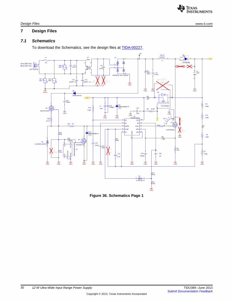
7 Design Files
7.1 SchematicsTo download the Schematics, see the design files at TIDA-00227.
Figure 36. Schematics Page 1
30 12-W Ultra-Wide Input Range Power Supply TIDU389–June 2013Submit Documentation Feedback
Copyright © 2013, Texas Instruments Incorporated

www.ti.com Design Files
Figure 37. Schematics Page 2
31TIDU389–June 2013 12-W Ultra-Wide Input Range Power SupplySubmit Documentation Feedback
Copyright © 2013, Texas Instruments Incorporated

Design Files www.ti.com
7.2 Bill of MaterialsTo download the bill of materials (BOM), see the design files at TIDA-00227.
Table 16. BOMPackageFitted Quantity Designator Description Part Number Manufacturer RoHS Reference
Fitted 1 !PCB1 Printed Circuit Board TIDA-00227 Any O
Fitted 3 B1, B2, B3 FERRITE CHIP 70 OHM 4000MA 0603 CIS10P700AC Samsung
Fitted 3 C1, C7, C37 CAP ALUM 33UF 35V 20% RADIAL 35YXJ33M5X11 Rubycon
Fitted 4 C2, C4, C9, C15 CAP FILM 0.47UF 560VDC RADIAL R46KI347050P1M Kemet
Fitted 1 C3 CAP ALUM 33UF 450V 20% RADIAL EKXG451ELL330MM20S Nippon 18x25 mm
Fitted 1 C6 CAP ALUM 15UF 450V 20% RADIAL EEU-EE2W150 Panasonic Y 12.5x25
Fitted 4 C8, C13, C14, C17 CAP CER 2200PF 300VAC 20% RADIAL VY2222M35Y5US63V7 Vishay
Fitted 2 C12, C16 CAP ALUM 470UF 35V 20% RADIAL EEU-FM1V471 Panasonic
Fitted 1 C18 CAP, CERM, 0.068uF, 50V, +/-10%, X7R, 0603 GRM188R71H683KA93D MuRata Y 0603
Fitted 1 C19 CAP CER 0.1UF 50V 10% X7R 0603 C0603C104K5RACTU Kemet
Fitted 2 C20, C30 CAP, CERM, 2200pF, 50V, +/-10%, X7R, 0603 C0603C222K5RAC Kemet
Fitted 1 C22 CAP CER 1UF 25V 10% X7R 0603 C0603C105K3RACTU Kemet
Fitted 1 C23 CAP, CERM, 22uF, 16V, +/-10%, X5R, 0805 C2012X5R1C226K125AC TDK Y 0805
Fitted 1 C24 CAP CER 470PF 50V 5% NP0 0603 06035A471JAT2A AVX Corporation
Fitted 1 C27 Corporation CAP CER 10000PF 630V 10% CH 1812 C4532CH2J103K160KA TDK Corporation 1812
Fitted 1 C31 CAP, CERM, 4.7uF, 50V, +/-10%, X5R, 0805 C2012X5R1H475K125AB TDK Y 0805
Fitted 1 C32 CAP, CERM, 1uF, 25V, +/-10%, X5R, 0805 08053D105KAT2A AVX Y 0805
Fitted 1 C33 CAP, CERM, 1000pF, 100V, +/-5%, X7R, 0603 06031C102JAT2A AVX Y 0603
Fitted 1 C34 CAP, CERM, 4700pF, 100V, +/-5%, X7R, 0603 06031C472JAT2A AVX Y 0603
Fitted 1 C36 CAP, CERM, 10uF, 25V, +/-20%, X5R, 0603 GRM188R61E106MA73 MuRata Y 0603
Fitted 1 D1 RECT BRIDGE GPP 8A 600V GBU GBU8J-BPMS Micro Commercial Co 0.880 x 0.140 inch
Micro CommercialFitted 1 D2 Diode, Zener, 27V, 3W, SMA 3SMAJ5935B-TP Y SMAComponents
Fitted 2 D3, D13 Diode, Signal, 300-mA, 75-V, 350-mW 1N4148W-7-F Diodes SOD-123
Fitted 1 D4 Diode, Zener,15-V, 1W SMAZ15 Diodes SMA
Fitted 1 D5 Diode, Ultrafast, 600V, 8A, DDPAK STTH8L06G ST Microelectronics Y DDPAK
Fitted 3 D6, D8, D9 Diode, Ultrafast, 600V, 1A, SMA MURA160T3G ON Semiconductor Y SMA
Micro CommercialFitted 1 D10 Diode, P-N, 200V, 200A, SOT-23 BAS21-TP Y SOT-23Components
Fitted 1 D11 Diode Schottky, 8A, 100V SS8PH10-M3/86A Vishay
Fitted 1 D12 Diode, Zener, 9.1V, 500mW, SOD-123 MMSZ5239B-7-F Diodes Inc. Y SOD-123
Fitted 1 D14 TVS DIODE 102VWM 165VC SMD P6SMB120A General SMB
Fitted 1 F1 FUSE SLOW 250VAC 5A RADIAL RST 5 BEL
Fitted 1 HT1 HEATSINK TO-220 W/PINS 1.5"TALL 513102B02500G Aavid Thermalloy 1.500x1.375in.
Fitted 1 with HT1 TO-220 Mounting Kit 4880G Aavid Thermalloy
Fitted 1 J1 Terminal Block, 30A, 9.52mm (.375) Pitch, 2-Pos, TH OSTT7022150 On-Shore Technology Y 19.62x21.5x12.5mm
32 12-W Ultra-Wide Input Range Power Supply TIDU389–June 2013Submit Documentation Feedback
Copyright © 2013, Texas Instruments Incorporated

www.ti.com Design Files
Table 16. BOM (continued)PackageFitted Quantity Designator Description Part Number Manufacturer RoHS Reference
TERM_BLK, 2pos,Fitted 1 J2 TERMINAL BLOCK 5.08MM VERT 2POS, TH ED120/2DS On-Shore Technology Y 5.08mm
Fitted 1 L1 INDUCTOR 150UH 4.0A 10% AIRD-06-151K Abracon Corporation Y 21 X 21 mm
Fitted 1 L2 Coupled inductor, 10mH, 5A, 0.055 ohm, TH 744825510 Wurth Elektronik eiSos Y 30x35x21mm
Fitted 1 L3 INDUCTOR 2.2UH 4.1A RADIAL LHL08TB2R2M Taiyo Yuden
Fitted 1 Q1 MOSFET, Nch, 600-V, 20A, 0.199 Ohms AOTF20S60L Alpha&Omega
Fitted 1 Q2 DISCRETE, MOSFET N-CH 500V 200MA, DPAK IXTY02N50D IXYS Y –
Fitted 2 Q4, Q7 MOSFET N-CH 60V 260MA SOT-23 2N7002ET1G OnSemi
Fitted 1 Q5 MOSFET N-CH 600V 21MA SOT23 BSS126 H6327 Infineon
Fitted 1 Q6 MOSFET, N-CH, 600V, 7A, DPAK AOD7N60 AOS Y DPAK
Fitted 1 R2 RES, 0 ohm, 5%, 0.25W, 1206 RC1206JR-070RL Yageo America Y 1206
Fitted 3 R3, R10, R11 RES 649K OHM 1/4W 1% 1206 SMD RC1206FR-07649KL Yageo
Fitted 1 R4 RES, 383k ohm, 1%, 0.1W, 0603 CRCW0603383KFKEA Vishay-Dale Y 0603
Fitted 1 R5 RES 0.02 OHM 1W 1% 2512 SMD LRMAM2512-R02FT4 TT/Welwyn
Fitted 1 R6 RES, 1.27k ohm, 1%, 0.1W, 0603 CRCW06031K27FKEA Vishay-Dale Y 0603
Fitted 1 R7 RES 3.83K OHM 1/10W 1% 0603 SMD RC0603FR-073K83L Yageo
Fitted 1 R8 RES, 220 ohm, 1%, 0.1W, 0603 RC0603FR-07220RL Yageo America Y 0603
Fitted 1 R9 RES 44.2K OHM 1/10W 1% 0603 SMD RC0603FR-0744K2L Yageo
Fitted 1 R12 RES 1.33M OHM 1/10W 1% 0603 SMD CRCW06031M33FKEA Vishay Dale
Fitted 1 R13 RES, 40.2k ohm, 1%, 0.1W, 0603 CRCW060340K2FKEA Vishay-Dale Y 0603
Fitted 1 R14 RES 15.0 OHM 1/8W 1% 0805 SMD RC0805FR-0715RL Yageo
Fitted 1 R15 RES, 4.02k ohm, 1%, 0.1W, 0603 RC0603FR-074K02L Yageo America Y 0603
Fitted 1 R16 RES, 1.00Meg ohm, 1%, 0.1W, 0603 CRCW06031M00FKEA Vishay-Dale Y 0603
Fitted 1 R17 RES, 127k ohm, 1%, 0.1W, 0603 CRCW0603127KFKEA Vishay-Dale Y 0603
Fitted 1 R18 RES, 402k ohm, 1%, 0.1W, 0603 CRCW0603402KFKEA Vishay-Dale Y 0603
Fitted 2 R20, R25 RES 30.1K OHM 1/10W 1% 0603 SMD RC0603FR-0730K1L Yageo
Fitted 1 R21 RES 1.00M OHM 1/10W 1% 0603 SMD RC0603FR-071ML Yageo
Fitted 1 R23 RES, 1.20 ohm, 1%, 1W, 2512 ERJ-1TRQF1R2U Panasonic Y 2512
Fitted 1 R24 RES 301K OHM 1/10W 1% 0603 SMD RC0603FR-07301KL Yageo
Fitted 1 R26 RES, 78.7k ohm, 1%, 0.1W, 0603 CRCW060378K7FKEA Vishay-Dale Y 0603
Fitted 2 R27, R41 RES, 1.00k ohm, 1%, 0.1W, 0603 CRCW06031K00FKEA Vishay-Dale Y 0603
Fitted 1 R28 RES 10.0 OHM 1/8W 1% 0805 SMD RC0805FR-0710RL Yageo
Fitted 1 R29 RES, 30.1k ohm, 1%, 0.1W, 0603 CRCW060330K1FKEA Vishay-Dale Y 0603
Fitted 5 R30, R34, R38, R40, R43 RES, 0 ohm, 5%, 0.1W, 0603 CRCW06030000Z0EA Vishay-Dale Y 0603
Fitted 1 R31 RES, 24.3k ohm, 1%, 0.1W, 0603 CRCW060324K3FKEA Vishay-Dale Y 0603
Fitted 1 R32 RES, 8.2 ohm, 5%, 0.75W, 2010 CRCW20108R20JNEF Vishay-Dale Y 2010
Fitted 1 R33 RES, 110k ohm, 5%, 0.1W, 0603 CRCW0603110KJNEA Vishay-Dale Y 0603
Fitted 1 R35 RES, 226k ohm, 1%, 0.1W, 0603 CRCW0603226KFKEA Vishay-Dale Y 0603
Fitted 1 R37 RES, 44.2k ohm, 1%, 0.1W, 0603 CRCW060344K2FKEA Vishay-Dale Y 0603
Fitted 1 R42 RES, 10k ohm, 5%, 0.1W, 0603 CRCW060310K0JNEA Vishay-Dale Y 0603
33TIDU389–June 2013 12-W Ultra-Wide Input Range Power SupplySubmit Documentation Feedback
Copyright © 2013, Texas Instruments Incorporated

Design Files www.ti.com
Table 16. BOM (continued)PackageFitted Quantity Designator Description Part Number Manufacturer RoHS Reference
Fitted 1 R44 RES, 4.99k ohm, 1%, 0.1W, 0603 CRCW06034K99FKEA Vishay-Dale Y 0603
Fitted 3 RT1, RT2, RT3 MOV, 300V MOV-10D471KTR Bourns
Fitted 1 T1 TRANSFOERMER, 856uH, +/-10%, TH, 14-PIN 750342415 WURTH ELEKTRONIK Y –
Fitted 1 U1 Opto-Isolator, 1 Channel, TH LTV-817 Lite-On Y DIP-4
Fitted 1 U2 IC REG CTRLR BST FLYBK CM 10MSOP TPS40210DGQ TI
Fitted 2 U3, U4 IC DETECTOR UNDER VOLT 3V SC70-5 LMS33460MG/NOPB TI
Constant-Voltage, Constant-Current Flyback Controller Using Opto-Fitted 1 U5 UCC28740D Texas Instruments Y D0007ACoupler Feedback, D0007A
Fitted 1 U6 IC VREF SHUNT PREC ADJ SOT23-3 TL431AIDBZT TI
H1, H2, H3, H4, H5, H6,Fitted 8 Mounting Hole M3 3.5mm STD STD Y ScrewH7, H8
FID1, FID2, FID3, FID4,Not Fitted 6 Fiducial mark. There is nothing to buy or mount. N/A N/A FiducialFID5, FID6
Not Fitted 0 C5, C26, C28, C35 CAP, CERM, 0.01uF, 1000V, +/-10%, X7R, 1210 GRM32QR73A103KW01L MuRata Y 1210
Not Fitted 0 C10, C11 CAP CER 330PF 300VAC 10% RADIAL VY2331K29Y5SS63V7 Vishay
Not Fitted 0 C21 CAP CER 470PF 50V 5% NP0 0603 06035A471JAT2A AVX Corporation
Not Fitted 0 C25, C29 CAP, CERM, 0.068uF, 50V, +/-10%, X7R, 0603 GRM188R71H683KA93D MuRata Y 0603
Micro CommercialNot Fitted 0 D7 Diode, TVS, Uni, 120V, 1500W, SMC SMCJ120A-TP Y SMCComponents
Not Fitted 0 Q3 MOSFET N-CH 600V 120MA SOT-223 BSP135 L6327 Infineon
Not Fitted 0 R1, R36 RES 330 OHM 1W 5% 2512 RC6432J331CS Samsung
Not Fitted 0 R19 RES 68 OHM 2W 1% 2512 RHC2512FT68R0 Stackpole Electronics Inc Y 2512
Not Fitted 0 R22 RES 162 OHM 1.5W 1% 2512 SMD CRCW2512162RFKEGHP Vishay-Dale Y 2512
Not Fitted 0 R39 RES, 0 ohm, 5%, 0.1W, 0603 CRCW06030000Z0EA Vishay-Dale Y 0603
Available Alternatives for BSS126:• TSM126 N-Channel Depletion-Mode MOSFET• KX1N60DS N-Channel Power MOSFET• GSM501DEA 600-V N-Channel Enhancement Mode MOSFET
34 12-W Ultra-Wide Input Range Power Supply TIDU389–June 2013Submit Documentation Feedback
Copyright © 2013, Texas Instruments Incorporated

www.ti.com Design Files
7.3 PCB LayoutTo download the layer plots, see the design files at TIDA-00227.
Figure 38. Silk Screen Top Overlay Figure 39. Top Solder Mask
Figure 40. Top Layer Figure 41. Bottom Layer
35TIDU389–June 2013 12-W Ultra-Wide Input Range Power SupplySubmit Documentation Feedback
Copyright © 2013, Texas Instruments Incorporated

Design Files www.ti.com
Figure 42. Bottom Solder Mask Figure 43. Bottom Overlay
Figure 44. Multilayer Composite
36 12-W Ultra-Wide Input Range Power Supply TIDU389–June 2013Submit Documentation Feedback
Copyright © 2013, Texas Instruments Incorporated

www.ti.com Design Files
7.4 Gerber FilesTo download the Gerber files, see the design files at TIDA-00227.
Figure 45. Fabrication Drawing
37TIDU389–June 2013 12-W Ultra-Wide Input Range Power SupplySubmit Documentation Feedback
Copyright © 2013, Texas Instruments Incorporated

Design Files www.ti.com
7.5 Assembly Drawings
Figure 46. Top Assembly Drawing Figure 47. Bottom Assembly Drawing
7.6 Software FilesTo download the software files, see the design files at TIDA-00227.
8 References
1. TPS40210, TPS40211 4.5-V to 52-V Input Current Mode Boost Controller (SLUS772)2. UCC28740 Constant-Voltage Constant-Current Flyback Controller Using Opto-Coupled Feedback
(SLUSBF3)3. Designing Magnetic Components for Optimum Performance in Low-Cost AC/DC Converter
Applications (SLUP265)4. AN-2162 Simple Success With Conducted EMI From DC-DC Converters (SNVA489)5. Understanding and Optimizing Electromagnetic Compatibility in Switchmode Power Supplies
(SLUP202)6. Inductor and Flyback Transformer Design (SLUP127)
9 About the AuthorKALLIKUPPA MUNIYAPPA SREENIVASA is a systems architect at Texas Instruments, where he isresponsible for developing reference design solutions for the industrial segment. Sreenivasa brings to thisrole his experience in high-speed digital and analog systems design. Sreenivasa earned his bachelor ofelectronics (BE) in electronics and communication engineering (BC-E&C) from VTU, Mysore, India.
SUNIL DWIVEDI is a systems engineer at Texas Instruments where he is responsible for developingreference design solutions for the industrial segment. Sunil brings to this role his experience in high-speeddigital and analog systems design. Sunil earned his bachelor of electronics (BE) in electronics andinstrumentation engineering (BE-E&I) from SGSITS, Indore, India.
38 12-W Ultra-Wide Input Range Power Supply TIDU389–June 2013Submit Documentation Feedback
Copyright © 2013, Texas Instruments Incorporated
IMPORTANT NOTICE FOR TI REFERENCE DESIGNS
Texas Instruments Incorporated ("TI") reference designs are solely intended to assist designers (“Buyers”) who are developing systems thatincorporate TI semiconductor products (also referred to herein as “components”). Buyer understands and agrees that Buyer remainsresponsible for using its independent analysis, evaluation and judgment in designing Buyer’s systems and products.TI reference designs have been created using standard laboratory conditions and engineering practices. TI has not conducted anytesting other than that specifically described in the published documentation for a particular reference design. TI may makecorrections, enhancements, improvements and other changes to its reference designs.Buyers are authorized to use TI reference designs with the TI component(s) identified in each particular reference design and to modify thereference design in the development of their end products. HOWEVER, NO OTHER LICENSE, EXPRESS OR IMPLIED, BY ESTOPPELOR OTHERWISE TO ANY OTHER TI INTELLECTUAL PROPERTY RIGHT, AND NO LICENSE TO ANY THIRD PARTY TECHNOLOGYOR INTELLECTUAL PROPERTY RIGHT, IS GRANTED HEREIN, including but not limited to any patent right, copyright, mask work right,or other intellectual property right relating to any combination, machine, or process in which TI components or services are used.Information published by TI regarding third-party products or services does not constitute a license to use such products or services, or awarranty or endorsement thereof. Use of such information may require a license from a third party under the patents or other intellectualproperty of the third party, or a license from TI under the patents or other intellectual property of TI.TI REFERENCE DESIGNS ARE PROVIDED "AS IS". TI MAKES NO WARRANTIES OR REPRESENTATIONS WITH REGARD TO THEREFERENCE DESIGNS OR USE OF THE REFERENCE DESIGNS, EXPRESS, IMPLIED OR STATUTORY, INCLUDING ACCURACY ORCOMPLETENESS. TI DISCLAIMS ANY WARRANTY OF TITLE AND ANY IMPLIED WARRANTIES OF MERCHANTABILITY, FITNESSFOR A PARTICULAR PURPOSE, QUIET ENJOYMENT, QUIET POSSESSION, AND NON-INFRINGEMENT OF ANY THIRD PARTYINTELLECTUAL PROPERTY RIGHTS WITH REGARD TO TI REFERENCE DESIGNS OR USE THEREOF. TI SHALL NOT BE LIABLEFOR AND SHALL NOT DEFEND OR INDEMNIFY BUYERS AGAINST ANY THIRD PARTY INFRINGEMENT CLAIM THAT RELATES TOOR IS BASED ON A COMBINATION OF COMPONENTS PROVIDED IN A TI REFERENCE DESIGN. IN NO EVENT SHALL TI BELIABLE FOR ANY ACTUAL, SPECIAL, INCIDENTAL, CONSEQUENTIAL OR INDIRECT DAMAGES, HOWEVER CAUSED, ON ANYTHEORY OF LIABILITY AND WHETHER OR NOT TI HAS BEEN ADVISED OF THE POSSIBILITY OF SUCH DAMAGES, ARISING INANY WAY OUT OF TI REFERENCE DESIGNS OR BUYER’S USE OF TI REFERENCE DESIGNS.TI reserves the right to make corrections, enhancements, improvements and other changes to its semiconductor products and services perJESD46, latest issue, and to discontinue any product or service per JESD48, latest issue. Buyers should obtain the latest relevantinformation before placing orders and should verify that such information is current and complete. All semiconductor products are soldsubject to TI’s terms and conditions of sale supplied at the time of order acknowledgment.TI warrants performance of its components to the specifications applicable at the time of sale, in accordance with the warranty in TI’s termsand conditions of sale of semiconductor products. Testing and other quality control techniques for TI components are used to the extent TIdeems necessary to support this warranty. Except where mandated by applicable law, testing of all parameters of each component is notnecessarily performed.TI assumes no liability for applications assistance or the design of Buyers’ products. Buyers are responsible for their products andapplications using TI components. To minimize the risks associated with Buyers’ products and applications, Buyers should provideadequate design and operating safeguards.Reproduction of significant portions of TI information in TI data books, data sheets or reference designs is permissible only if reproduction iswithout alteration and is accompanied by all associated warranties, conditions, limitations, and notices. TI is not responsible or liable forsuch altered documentation. Information of third parties may be subject to additional restrictions.Buyer acknowledges and agrees that it is solely responsible for compliance with all legal, regulatory and safety-related requirementsconcerning its products, and any use of TI components in its applications, notwithstanding any applications-related information or supportthat may be provided by TI. Buyer represents and agrees that it has all the necessary expertise to create and implement safeguards thatanticipate dangerous failures, monitor failures and their consequences, lessen the likelihood of dangerous failures and take appropriateremedial actions. Buyer will fully indemnify TI and its representatives against any damages arising out of the use of any TI components inBuyer’s safety-critical applications.In some cases, TI components may be promoted specifically to facilitate safety-related applications. With such components, TI’s goal is tohelp enable customers to design and create their own end-product solutions that meet applicable functional safety standards andrequirements. Nonetheless, such components are subject to these terms.No TI components are authorized for use in FDA Class III (or similar life-critical medical equipment) unless authorized officers of the partieshave executed an agreement specifically governing such use.Only those TI components that TI has specifically designated as military grade or “enhanced plastic” are designed and intended for use inmilitary/aerospace applications or environments. Buyer acknowledges and agrees that any military or aerospace use of TI components thathave not been so designated is solely at Buyer's risk, and Buyer is solely responsible for compliance with all legal and regulatoryrequirements in connection with such use.TI has specifically designated certain components as meeting ISO/TS16949 requirements, mainly for automotive use. In any case of use ofnon-designated products, TI will not be responsible for any failure to meet ISO/TS16949.IMPORTANT NOTICE
Mailing Address: Texas Instruments, Post Office Box 655303, Dallas, Texas 75265Copyright © 2014, Texas Instruments Incorporated