pcb design support for coaxial connector related... · pcb design support for coaxial connector...
TRANSCRIPT
PCB design Support for Coaxial connector
Hirose Electric Co., Ltd.
Oct 2015
1
RF-14547-02
Outline
• Introduction
• Mechanical performance
• Products
• Specifications
• Electrical performance
• PCB design considerations
• Appendix
2

3
Introduction
◆ Purpose
◆ Scope
◆ Application and Interpretation High Frequency Measurement Fixture
IT5 Demo board
Used as test ports for high-speed, high-pin-count signals
Show the simulation and measurement results using 2.4mm,2.92mm
vertical mount RF connector.
Excellent performance connector for test port with screw mount up to 50GHz.
Realizes good electrical performance with stub-less structure and
easy assembly with screw mount.
This design guide provides the information of product performance and PCB
design in order to obtain full performance of the connectors.
This connector allows
high density test port layout due to
its vertical mount feature ,which also
provides flexible pattern design.
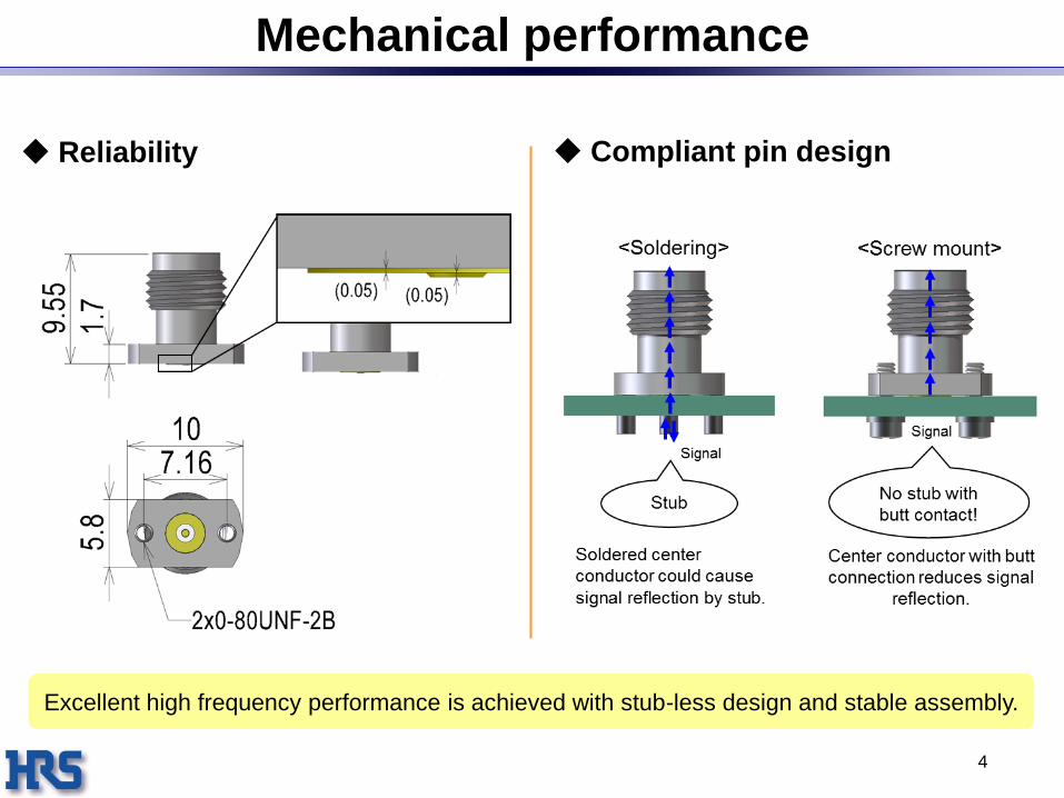
Mechanical performance
Excellent high frequency performance is achieved with stub-less design and stable assembly.
Reliability Compliant pin design
4
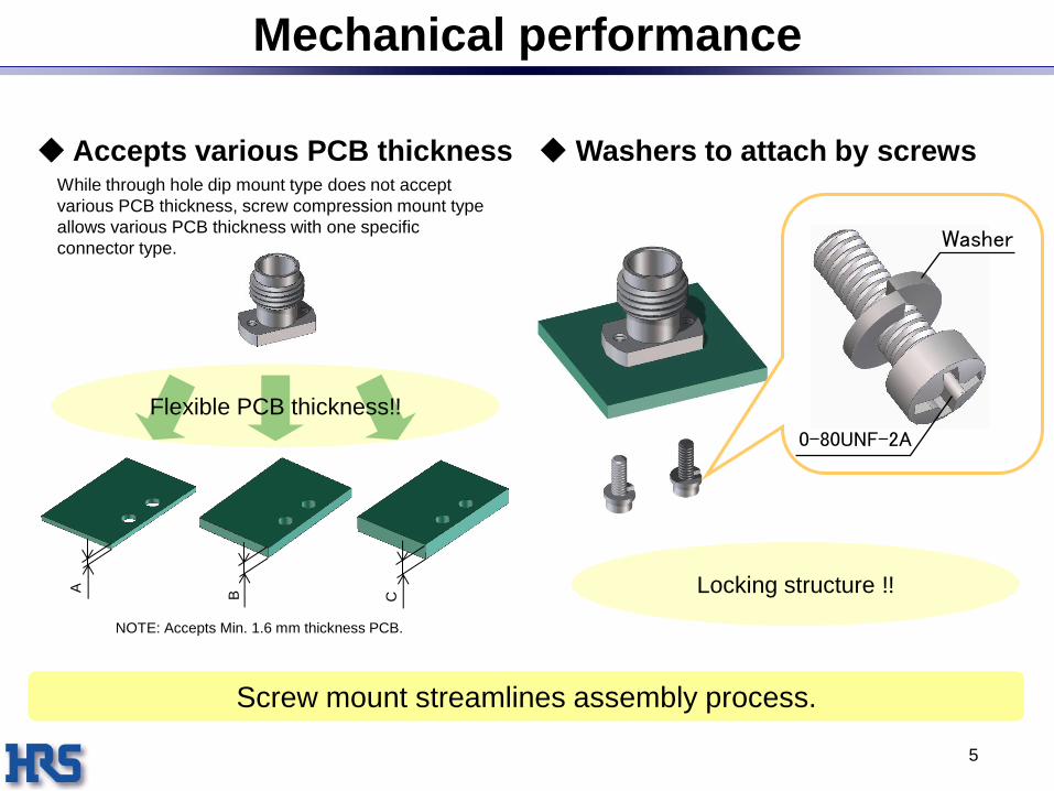
Mechanical performance
5
Screw mount streamlines assembly process.
Accepts various PCB thickness Washers to attach by screws
Flexible PCB thickness!!
While through hole dip mount type does not accept
various PCB thickness, screw compression mount type
allows various PCB thickness with one specific
connector type.
C
B A
NOTE: Accepts Min. 1.6 mm thickness PCB.
Washer
0-80UNF-2A
Locking structure !!
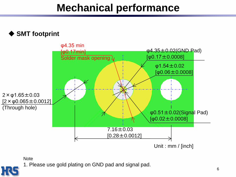
SMT footprint
Mechanical performance
Note
1. Please use gold plating on GND pad and signal pad.
φ4.35±0.02(GND Pad)
[φ0.17±0.0008]
φ1.54±0.02
[φ0.06±0.0008]
φ0.51±0.02(Signal Pad)
[φ0.02±0.0008]
2×φ1.65±0.03
[2×φ0.065±0.0012]
(Through hole)
7.16±0.03
[0.28±0.0012]
Unit : mm / [inch]
6
φ4.35 min
[φ0.17min]
Solder mask opening

7
Products
Performance of a 2.4mm and 2.92mm connector thru
measurements to be shown.
2.4mm
Range: 0 to 50GHz
2.92mm
Range: 0 to 40GHz
( H2.4-R-SR2 ) ( HK-R-SR2-1 )
8
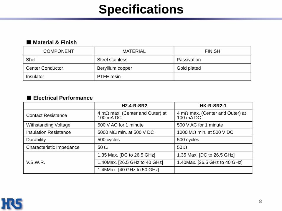
■ Material & Finish
COMPONENT MATERIAL FINISH
Shell Steel stainless Passivation
Center Conductor Beryllium copper Gold plated
Insulator PTFE resin -
Specifications
■ Electrical Performance
H2.4-R-SR2 HK-R-SR2-1
Contact Resistance 4 m max. (Center and Outer) at 100 mA DC
4 m max. (Center and Outer) at 100 mA DC
Withstanding Voltage 500 V AC for 1 minute 500 V AC for 1 minute
Insulation Resistance 5000 M min. at 500 V DC 1000 M min. at 500 V DC
Durability 500 cycles 500 cycles
Characteristic Impedance 50 50
V.S.W.R.
1.35 Max. [DC to 26.5 GHz] 1.35 Max. [DC to 26.5 GHz]
1.40Max. [26.5 GHz to 40 GHz] 1.40Max. [26.5 GHz to 40 GHz]
1.45Max. [40 GHz to 50 GHz]
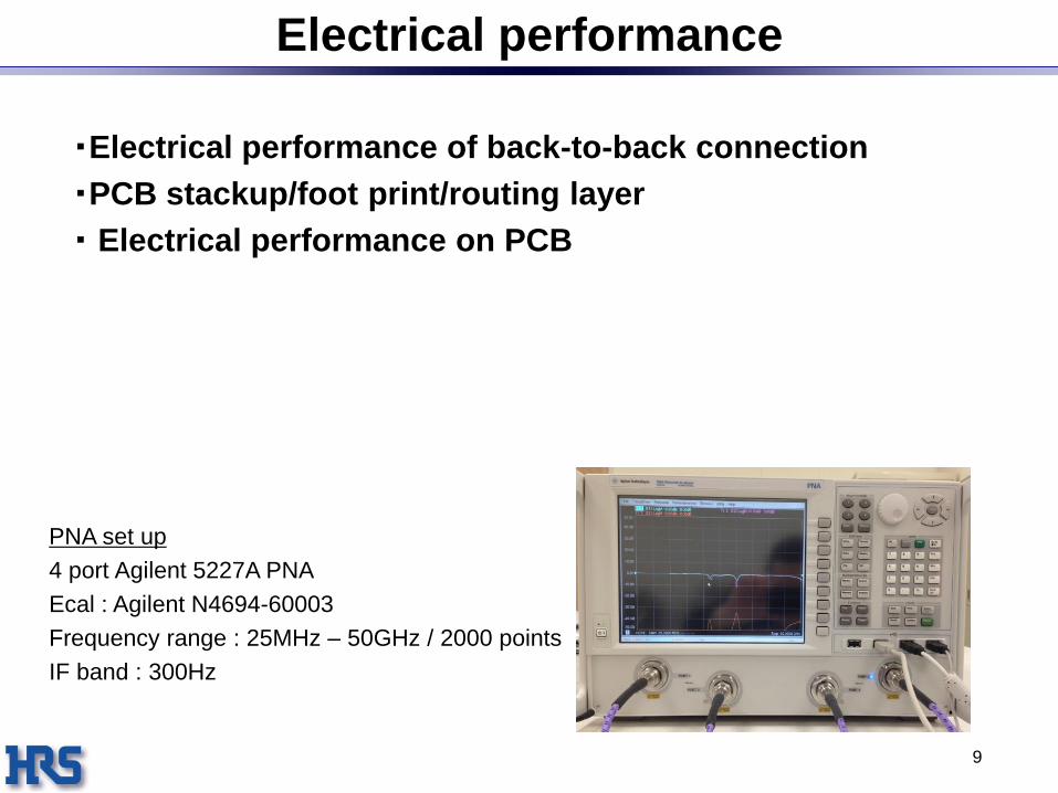
Electrical performance
・Electrical performance of back-to-back connection
・PCB stackup/foot print/routing layer
・ Electrical performance on PCB
9
PNA set up
4 port Agilent 5227A PNA
Ecal : Agilent N4694-60003
Frequency range : 25MHz – 50GHz / 2000 points
IF band : 300Hz
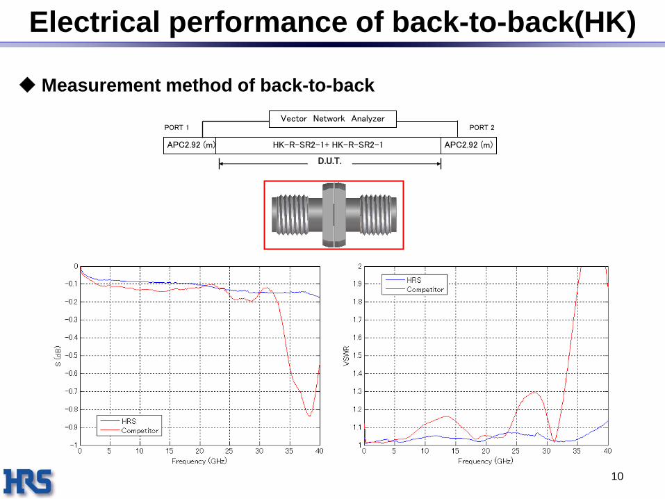
Electrical performance of back-to-back(HK)
Measurement method of back-to-back
Vector Network Analyzer
APC2.92 (m) APC2.92 (m)
PORT 2 PORT 1
D.U.T.
HK-R-SR2-1+ HK-R-SR2-1
10

Electrical performance of back-to-back(H2.4)
Measurement method by back-to-back
Vector Network Analyzer
APC2.4 (m) APC2.4 (m)
PORT 2 PORT 1
D.U.T.
H2.4-R-SR2+ H2.4-R-SR2
11

SMT land for coaxial connector
PCB stackup/foot print/routing layer
PCB stackup
Evaluation PCB
Bottom
Routing layer
43micron (Copper foil + Plating)
18micron (Copper foil)
100micron (Megtron 6 R5775K #3313)
70micron (Megtron 6 R5670 #1080)
200micron (Megtron 6 R5775K #3313)
18micron (Copper foil)
70micron (Megtron 6 R5670 #1080)
18micron (Copper foil)
200micron (Megtron 6 R5775K #3313)
43micron (Copper foil + Plating)
Top
2nd
3rd
4th
25mm [984mils]
solder mask
12
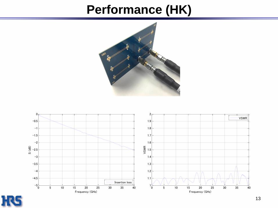
Performance (HK)
0 5 10 15 20 25 30 35 401
1.1
1.2
1.3
1.4
1.5
1.6
1.7
1.8
1.9
2
Frequency (GHz)
VS
WR
VSWR
0 5 10 15 20 25 30 35 40-5
-4.5
-4
-3.5
-3
-2.5
-2
-1.5
-1
-0.5
0
Frequency (GHz)
S (
dB)
Insertion loss
13
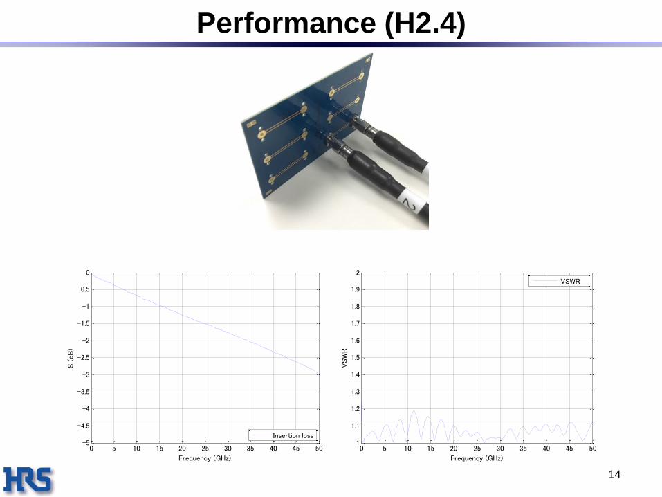
Performance (H2.4)
0 5 10 15 20 25 30 35 40 45 501
1.1
1.2
1.3
1.4
1.5
1.6
1.7
1.8
1.9
2
Frequency (GHz)
VS
WR
VSWR
0 5 10 15 20 25 30 35 40 45 50-5
-4.5
-4
-3.5
-3
-2.5
-2
-1.5
-1
-0.5
0
Frequency (GHz)
S (
dB)
Insertion loss
14
PCB design considerations
15
・Optimized GND via locations for 50GHz
・Tapered trace and diving board design
・Via stub impact
・Consideration of copper wicking
・Stitching via space recommendation for CPWG
・Stitching via separation recommendation for CPWG
・Substrate thickness between 2 GND planes
・Antipad optimization(thick PCB)
・Antipad optimization(thin PCB)
・The effect of glass weave style
・Surface roughness of copper foil
・Measurement vs. simulation correlation

Tapered trace and diving board design
Tapering signal pad to trace and pushing out GND, referred to as “diving board” design,
achieves better impedance matching in the anti pad area and improves insertion loss and
return loss beyond 35GHz.
Tapered pad to trace transition
& Diving board structure
Simulation
5.1mm[200 mil] strip line
Megtron 6 (Dk : 3.6, Df : 0.004)
2.4 mm coaxial
connector
Drill diameter
Signal: 0.25mm [10mils]
Ground: inner ring 0.25mm [10mils]
/outer ring 0.3mm [12mils]
17
trace
Diving board
Tapered signal pad
GND plane
Signal via

Via stub impact
For inner layer routing, via stub length shall be minimized to be less than 1.3mm [5 mils]
for 50GHz. 0.5mm [20 mil] via stub will cause non-linear effects on insertion loss and
return loss.
Leftover via stub
27.4mm [1080 mil] strip line
Megtron 6 (Dk : 3.6, Df : 0.004)
2.4 mm coaxial
connector
Measurement
Drill diameter
Signal: 0.25mm [10mils]
Ground: inner ring 0.25mm [10mils]
/outer ring 0.3mm [12mils]
18
Consideration of copper wicking
Wicking example Cross section of via
When substrate is drilled, damaged glass fibers and separation in the glass fibers to the resin
leave holes. Because of migration of copper salt into the glass fibers of insulation material,
these holes will be filled with copper during the electro-plating process. It will cause a
discrepancy between design and actual PCB.
To compensate for copper wicking, 5% to 10% of diameter is added to diameter of signal via
model.
19
Via anode side (+) Via cthode side (-)
Cu++
Cu++
Cu++
Cu++
Cu++
Damaged glass fibers
Tiny clearance Drill size
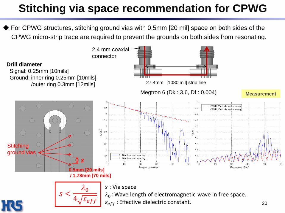
Stitching via space recommendation for CPWG
For CPWG structures, stitching ground vias with 0.5mm [20 mil] space on both sides of the
CPWG micro-strip trace are required to prevent the grounds on both sides from resonating.
Stitching
ground vias
0.5mm [20 mils]
/ 1.78mm [70 mils]
Drill diameter
Signal: 0.25mm [10mils]
Ground: inner ring 0.25mm [10mils]
/outer ring 0.3mm [12mils] 27.4mm [1080 mil] strip line
Megtron 6 (Dk : 3.6, Df : 0.004)
2.4 mm coaxial
connector
Measurement
20
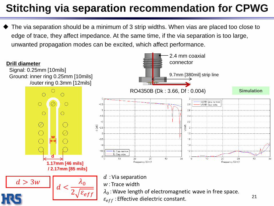
Stitching via separation recommendation for CPWG
9.7mm [380mil] strip line
RO4350B (Dk : 3.66, Df : 0.004)
2.4 mm coaxial
connector
Simulation
Drill diameter
Signal: 0.25mm [10mils]
Ground: inner ring 0.25mm [10mils]
/outer ring 0.3mm [12mils]
The via separation should be a minimum of 3 strip widths. When vias are placed too close to
edge of trace, they affect impedance. At the same time, if the via separation is too large,
unwanted propagation modes can be excited, which affect performance.
1.17mm [46 mils]
/ 2.17mm [85 mils]
w
21
d

Substrate thickness between 2 GND planes
Simulation
t=2
mm
/
[5
08
mil
s]
t=0
.2m
m/
[
51
mil
s]
RO4350B (Dk : 3.66, Df : 0.004)
If substrate thickness is too large, unwanted spurious wave propagation can occur. It can
interfere with the desired wave on the circuit.
Thin PCB substrate
Thick PCB substrate
22
9.7mm [380mil] strip line
2.4 mm coaxial
connector

Anti-pad optimization (thick PCB)
Antipad size is optimized at every layer by considering dielectric layer thickness and via
pad size.
Layer Anti-pad dia.
Top 1.5mm / [59 mils]
2 1.5mm / [59 mils]
Layer 3-24 0.94mm / [37 mils]
Layer 25 1mm / [40 mils]
Bottom Microstrip line out
PCB stackup
Megtron 6 (Dk : 3.6, Df : 0.004)
2.4 mm coaxial
connector
PTH anti-pad dimensions 23
Bottom
Routing layer
2.0mil (Copper foil + Plating)
4.72mil (Megtron 6 #1078)
3.7mil (Megtron 6 #3313)
solder mask Top
2
3
4
5
6
7
8
9
10
11
12
13
14
15
16
17
18
19
20
21
22
23
24
25
0.6mil (Copper foi)
6.46mil (Megtron 6 #1078)
3.94mil (Megtron 6 #3313)
0.6mil (Copper foi)
0.6mil (Copper foi)
0.6mil (Copper foi)
3.2mil (Megtron 6 #3313)
0.6mil (Copper foi)
4.72mil (Megtron 6 #1078)
3.52mil (Megtron 6 #3313)
4.72mil (Megtron 6 #1078)
6.46mil (Megtron 6 #1078)
3.94mil (Megtron 6 #3313)
6.46mil (Megtron 6 #1078)
4.72mil (Megtron 6 #1078)
3.52mil (Megtron 6 #3313)
4.72mil (Megtron 6 #1078)
6.46mil (Megtron 6 #1078)
3.94mil (Megtron 6 #3313)
6.46mil (Megtron 6 #1078)
4.72mil (Megtron 6 #1078)
3.52mil (Megtron 6 #3313)
4.72mil (Megtron 6 #1078)
3.2mil (Megtron 6 #3313)
3.94mil (Megtron 6 #3313)
3.7mil (Megtron 6 #3313)
4.72mil (Megtron 6 #1078)
6.46mil (Megtron 6 #1078)
0.6mil (Copper foi)
0.6mil (Copper foi)
0.6mil (Copper foi)
0.6mil (Copper foi)
0.6mil (Copper foi)
0.6mil (Copper foi)
0.6mil (Copper foi)
0.6mil (Copper foi)
0.6mil (Copper foi)
0.6mil (Copper foi)
0.6mil (Copper foi)
0.6mil (Copper foi)
0.6mil (Copper foi)
0.6mil (Copper foi)
0.6mil (Copper foi)
0.6mil (Copper foi)
0.6mil (Copper foi)
0.6mil (Copper foi)
0.6mil (Copper foi)
2.0mil (Copper foil + Plating)

Anti-pad optimization (thin PCB)
Antipad size is optimized at every layer by considering dielectric layer thickness and via
pad size.
PCB stackup
Bottom
Routing layer
1.7mil (Copper foil + Plating)
0.6mil (Copper foil)
4mil (Megtron 6 #3313)
2.76mil (Megtron 6 #1080)
7.87mil (Megtron 6 #3313)
0.6mil (Copper foil)
2.76mil (Megtron 6 #1080)
18mil (Copper foil)
7.87mil (Megtron 6 #3313)
1.7mil (Copper foil + Plating)
Top
2nd
3rd
4rd
solder mask
Layer Anti-pad dia.
Top 1.54mm/ [60.6mils]
2 1.15mm/ [45.3mils]
3 0.97mm/ [38.2mils]
4 1.09mm/ [42.9mils]
Bottom 1.02mm/ [40.2mils]
PTH anti-pad dimensions 24
Megtron 6 (Dk : 3.6, Df : 0.004)
2.4 mm coaxial
connector
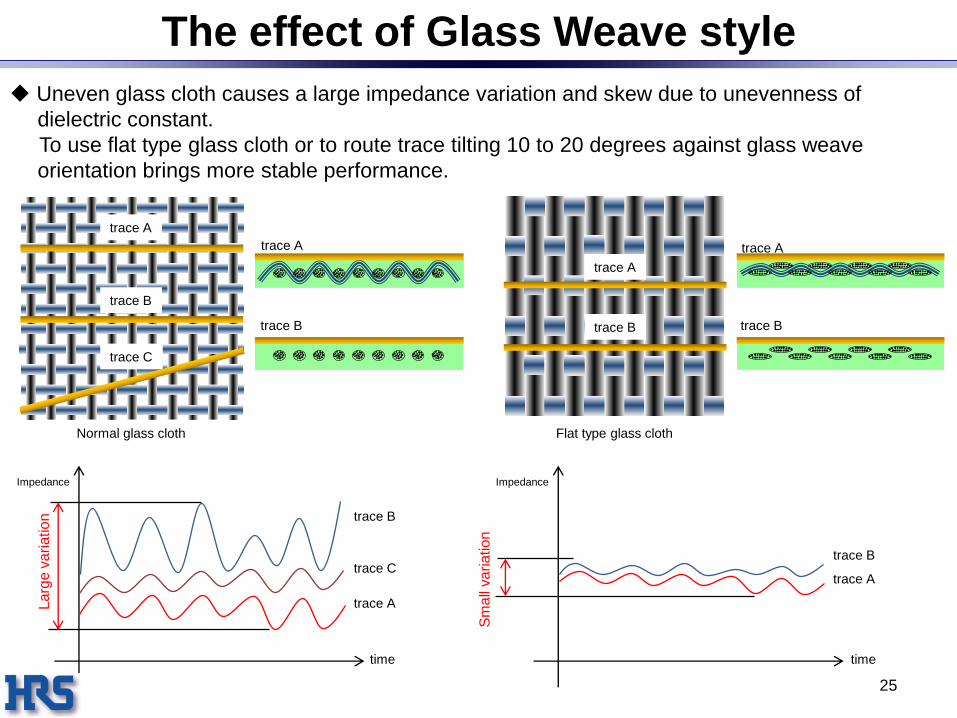
The effect of Glass Weave style
trace A trace A
trace A
trace B
trace A
trace B trace B trace B
Uneven glass cloth causes a large impedance variation and skew due to unevenness of
dielectric constant.
To use flat type glass cloth or to route trace tilting 10 to 20 degrees against glass weave
orientation brings more stable performance.
time
Impedance
trace A
trace B
trace A
trace B
Impedance
Normal glass cloth
Larg
e v
ariatio
n
Sm
all
va
riatio
n
Flat type glass cloth
time
trace C
trace C
25

Typical glass weave styles
Style Fabric Count Warp x Fill
(Per cm) Yarn (SI)
Thickness (mm) (Reference Only)
Nominal Weight (g/m2)
Weight Tolerance (g/m2)
101 29.5 x 29.5 5 2.75 1x0 5 2.75 1x0 0.024 16.3 15.2 - 17.3 1
104 23.6 x 20.5 5 5.5 1x0 5 2.75 1x0 0.028 18.6 18.0 - 19.3 1
106 22.0 x 22.0 5 5.5 1x0 5 5.5 1x0 0.033 24.4 23.4 - 25.4 1
1078 21.3 x 21.3 5 11 1x0 5 11 1x0 0.043 47.8 46.8 - 49.2 1
1080 23.6 x 18.5 5 11 1x0 5 11 1x0 0.053 46.8 45.1 - 48.5 1
1081 27.6 x 23.6 5 11 1x0 5 11 1x0 0.06 58.3 56.4 - 60.6 1
1280 23.6 x 23.6 5 11 1x0 5 11 1x0 0.056 52.9 51.5 - 54.2 1
1500 19.3 x 16.5 7 45 1x0 7 45 1x0 0.149 164.1 157.7 - 170.5 1
1501 18.1 x 17.7 7 45 1x0 7 45 1x0 0.14 165 158.0 - 171.0 1
1504 23.6 x 19.7 6 33 1x0 6 33 1x0 0.125 148 142.8 - 153.2 1
1651 20.0 x 10.8 9 33 1x0 9 74 1x0 0.135 146.2 142.1 - 150.3 1
1652 20.5 x 20.5 9 34 1x0 9 34 1x0 0.114 138.3 133.6 - 143.1 1
1674 15.7 x 12.6 9 34 1x0 9 34 1x0 0.097 96.6 92.9 - 100.4 1
1675 15.7 x 12.6 6 33 1x0 6 33 1x0 0.101 96.3 92.6 - 100.0 1
1678 15.7 x 15.7 9 34 1x0 9 34 1x0 0.091 103.5 102.7 - 111.6 1
2113 23.6 x 22.0 7 22 1x0 5 11 1x0 0.079 78 75.6 - 80.4 1
2114 22.0 x 18.9 7 22 1x0 7 22 1x0 0.084 90.9 88.5 - 93.2 1
2116 23.6 x 22.8 7 22 1x0 7 22 1x0 0.094 103.8 100.7 - 106.8 1
2117 26.0 x 21.7 7 22 1x0 7 22 1x0 0.095 108 104.8 - 111.2 1
2125 15.7 x 15.4 7 22 1x0 9 34 1x0 0.091 87.5 82.7 - 90.9 1
2157 23.6 x 13.8 7 22 1x0 9 68 1X0 0.13 148 144.0 - 152.0 1
2165 23.6 x 20.5 7 22 1x0 9 34 1x0 0.101 122.4 116.3 - 126.1 1
2166 23.6 x 15.0 7 22 1x0 9 68 1X0 0.14 155 150.0 - 160.0 1
2313 23.6 x 25.2 7 22 1x0 5 11 1x0 0.084 81.4 79.0 - 83.7 1
3070 27.6 x 27.6 6 16.5 1x0 6 16.5 1x0 0.078 93.6 90.9 - 96.3 1
3080 20.0 x 12.0 6 16.5 1x0 6 16.5 1x0 0.059 53.4 51.5 - 55.3 1
3313 23.6 x 24.4 6 16.5 1x0 6 16.5 1x0 0.084 81.4 79.0 - 83.7 1
7628 17.3 x 12.2 9 68 1x0 9 68 1x0 0.173 203.4 198.0 - 208.9 1
7629 17.3 x 13.4 9 68 1x0 9 68 1x0 0.18 210 204.5 - 215.3 1
7635 17.3 x 11.4 9 68 1x0 9 102 1x0 0.201 232.3 226.5 - 238.0 1
7642 17.3 x 7.9 (texturized) 9 68 1x0 9 136 1x0 0.254 227.8 221.1 - 234.7 1
※Quotation from IPC-4412
26
Good flat type is available
Flat type is available

trace
GND
substrate
Surface roughness of copper foil
trace
GND
substrate
trace
GND
substrate
At high frequencies, rough copper foil will cause large attenuation. Choosing smoother
copper foil will provide improved quality on high frequency transmission line. However,
smoother copper foil has less peel strength between substrate and copper. So, it is
important to choose suitable copper foil by balancing mechanical issue and electrical
issue.
・Standard foil
ED:Electrodeposited
HTE:High Tensile Elongation
・Low profile
RTF:Reverse Treated Foil
VLP:Very Low Profile
・Very low profile
e-VPL:Extra Very Low Profile
H-VLP:Hyper Very Low Profile
>10 microns
5 -10 microns
<5 microns
Copper foil type Peel strength Stable impedance Attenuation Cost
Standard foil
Low profile
Very low profile 27
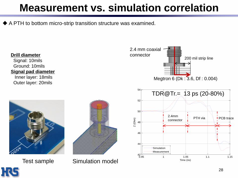
Measurement vs. simulation correlation
0.95 1 1.05 1.1 1.1542
44
46
48
50
52
54
Time (ns)
Z (
Ohm
)
Simulation
Measurement
2.4mm
connector PTH via PCB trace
A PTH to bottom micro-strip transition structure was examined.
TDR@Tr.= 13 ps (20-80%)
Test sample
200 mil strip line
Megtron 6 (Dk : 3.6, Df : 0.004)
Drill diameter
Signal: 10mils
Ground: 10mils
Signal pad diameter
Inner layer: 18mils
Outer layer: 20mils
Simulation model
2.4 mm coaxial
connector
28
Appendix
・Cutoff frequency
・2.4mm, 2.92mm comparison
・Conversion of VSWR to Return loss
29
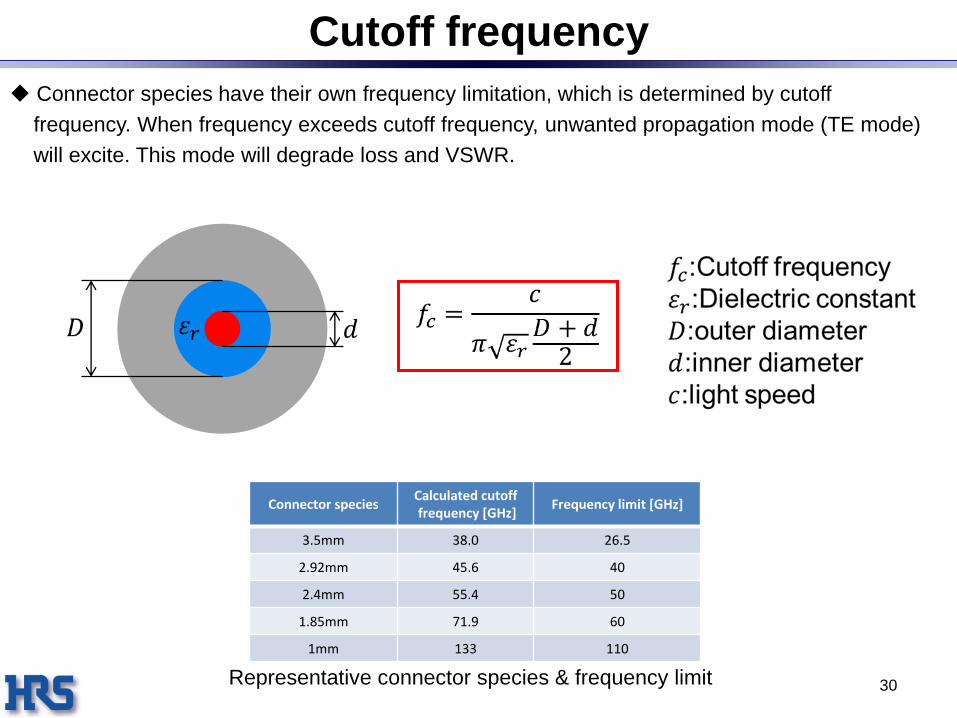
Cutoff frequency
Connector species have their own frequency limitation, which is determined by cutoff
frequency. When frequency exceeds cutoff frequency, unwanted propagation mode (TE mode)
will excite. This mode will degrade loss and VSWR.
Connector species Calculated cutoff frequency [GHz]
Frequency limit [GHz]
3.5mm 38.0 26.5
2.92mm 45.6 40
2.4mm 55.4 50
1.85mm 71.9 60
1mm 133 110
Representative connector species & frequency limit 30

2.4mm,2.92mm comparison
Back to back measurement
0 5 10 15 20 25 30 35 40 45 501
1.2
1.4
1.6
1.8
2
2.2
2.4
2.6
2.8
3
Frequency (GHz)
VS
WR
VSWR 2.4mmVSWR 2.92mm
0 5 10 15 20 25 30 35 40 45 50-5
-4.5
-4
-3.5
-3
-2.5
-2
-1.5
-1
-0.5
0
Frequency (GHz)
S (
dB)
IL 2.4mmIL 2.92mm
Degradation due to unwanted mode Degradation due to unwanted mode
31

Conversion of VSWR and Return loss
VSWR Return loss [dB]
1 -
1.05 -32.26
1.1 -26.44
1.2 -20.83
1.3 -17.69
1.4 -15.56
1.5 -13.98
1.6 -12.74
1.7 -11.73
1.8 -10.88
1.9 -10.16
2 -9.54
2.5 -7.36
3 -6.02
3.5 -5.11
4 -4.44
4.5 -3.93
5 -3.52
Return loss [dB] VSWR
-40 1.02
-30 1.07
-20 1.22
-15 1.43
-10 1.92
-5 3.57
VSWR to Return loss Return loss to VSWR
32