parallel instruction decoding for dsp controllers with...
TRANSCRIPT

Master of Science Thesis in Electrical EngineeringDepartment of Electrical Engineering, Linköping University, 2019
Parallel instruction decodingfor DSP controllers withdecoupled execution units
Andreas Pettersson
Master of Science Thesis in Electrical Engineering
Parallel instruction decoding for DSP controllers with decoupled executionunits:
Andreas Pettersson
LiTH-ISY-EX--19/5218--SE
Supervisor: Oscar Gustafssonisy, Linköping University
Andréas KarlssonMediaTek Sweden AB
Examiner: Kent Palmkvistisy, Linköping University
Division of Computer EngineeringDepartment of Electrical Engineering
Linköping UniversitySE-581 83 Linköping, Sweden
Copyright © 2019 Andreas Pettersson

AbstractApplications run on embedded processors are constantly evolving. They are forthe most part growing more complex and the processors have to increase theirperformance to keep up. In this thesis, an embedded DSP SIMT processor withdecoupled execution units is under investigation. A SIMT processor exploits theparallelism gained from issuing instructions to functional units or to decoupledexecution units. In its basic form only a single instruction is issued per cycle. Ifthe control of the decoupled execution units become too fine-grained or if thecontrol burden of the master core becomes sufficiently high, the fetching anddecoding of instructions can become a bottleneck of the system.
This thesis investigates how to parallelize the instruction fetch, decode and issueprocess. Traditional parallel fetch and decode methods in superscalar and VLIWarchitectures are investigated. Benefits and drawbacks of the two are presentedand discussed. One superscalar design and one VLIW design are implementedin RTL, and their costs and performances are compared using a benchmark pro-gram and synthesis. It is found that both the superscalar and the VLIW designsoutperform a baseline scalar processor as expected, with the VLIW design per-forming slightly better than the superscalar design. The VLIW design is found tobe able to achieve a higher clock frequency, with an area comparable to the areaof the superscalar design.
This thesis also investigates how instructions can be encoded to lower the decodecomplexity and increase the speed of issue to decoupled execution units. A num-ber of possible encodings are proposed and discussed. Simulations show thatthe encodings have a possibility to considerably lower the time spent issuing todecoupled execution units.
iii


AcknowledgmentsI would like to express my sincere gratitude to my supervisor Andréas Karlssonat MediaTek for all the help, input and interesting discussions, both on- and off-topic. No question has been too small or too big. I would also like to thankeveryone else at the Linköping site for their help and for their part in makingthis time very enjoyable.
This thesis concludes my studies at Linköping University and these five yearshave been wonderful. I have learned so much and am especially grateful for allthe friends I have made. You are the reason these years have been so fantasticand I wish all of you the best. Finally, I would like to thank my family for youreverlasting support.
Linköping, June 2019Andreas Pettersson
v


Contents
Notation ix
1 Introduction 11.1 Background . . . . . . . . . . . . . . . . . . . . . . . . . . . . . . . 1
1.1.1 Processor tasks . . . . . . . . . . . . . . . . . . . . . . . . . 21.1.2 The BBP2 processor . . . . . . . . . . . . . . . . . . . . . . . 2
1.2 Problem definition . . . . . . . . . . . . . . . . . . . . . . . . . . . 31.3 Thesis outline . . . . . . . . . . . . . . . . . . . . . . . . . . . . . . 3
2 Theory 52.1 Computer architectures . . . . . . . . . . . . . . . . . . . . . . . . . 5
2.1.1 Single Instruction stream-Single Data stream architecture . 52.1.2 Scalar processor . . . . . . . . . . . . . . . . . . . . . . . . . 52.1.3 Superscalar processor . . . . . . . . . . . . . . . . . . . . . . 62.1.4 Very Long Instruction Word processor . . . . . . . . . . . . 62.1.5 Single Instruction stream-Multiple Data streams . . . . . . 62.1.6 Vector processor . . . . . . . . . . . . . . . . . . . . . . . . . 6
2.2 Conflicts . . . . . . . . . . . . . . . . . . . . . . . . . . . . . . . . . 62.2.1 Data conflict . . . . . . . . . . . . . . . . . . . . . . . . . . . 72.2.2 Structural conflict . . . . . . . . . . . . . . . . . . . . . . . . 72.2.3 Control conflict . . . . . . . . . . . . . . . . . . . . . . . . . 7
2.3 Digital Signal Processor . . . . . . . . . . . . . . . . . . . . . . . . . 8
3 Master core architecture design 93.1 Architecture design choices . . . . . . . . . . . . . . . . . . . . . . 9
3.1.1 In-order vs. out-of-order superscalar . . . . . . . . . . . . . 93.1.2 Number of superscalar ways . . . . . . . . . . . . . . . . . . 123.1.3 Memory and code size . . . . . . . . . . . . . . . . . . . . . 143.1.4 VLIW instruction encoding . . . . . . . . . . . . . . . . . . 143.1.5 Superscalar instruction encoding . . . . . . . . . . . . . . . 18
3.2 Superscalar vs. VLIW . . . . . . . . . . . . . . . . . . . . . . . . . . 193.2.1 Issue and stalling of instructions with uncertain latencies . 193.2.2 Instruction packaging around branch targets . . . . . . . . 21
vii

viii Contents
4 Master core implementation results 254.1 Implementation . . . . . . . . . . . . . . . . . . . . . . . . . . . . . 254.2 Compilers . . . . . . . . . . . . . . . . . . . . . . . . . . . . . . . . 264.3 CoreMark benchmark results . . . . . . . . . . . . . . . . . . . . . 274.4 Synthesis results . . . . . . . . . . . . . . . . . . . . . . . . . . . . . 29
5 Issue to decoupled execution units 335.1 Motivation . . . . . . . . . . . . . . . . . . . . . . . . . . . . . . . . 335.2 Instruction encoding for enhanced issue . . . . . . . . . . . . . . . 34
5.2.1 Issue speedup with grouped instructions . . . . . . . . . . . 365.2.2 Fetch bandwidth and instruction buffers . . . . . . . . . . . 39
6 Conclusions and future work 456.1 Conclusions . . . . . . . . . . . . . . . . . . . . . . . . . . . . . . . 456.2 Suggestions for future work . . . . . . . . . . . . . . . . . . . . . . 46
Bibliography 47

Notation
Abbreviations
Abbreviation Meaning
ALU Arithmetic Logic UnitASIC Application Specific Integrated CircuitASIP Application Specific Instruction set ProcessorCISC Complex Instruction Set ComputerDSP Digital Signal Processing or Digital Signal ProcessorEU Execution UnitFU Functional Unit
GP-DSP General Purpose Digital Signal ProcessorGPP General Purpose ProcessorIM Instruction Memory
LSU Load-Store UnitMAC Multiplier-AccumulatorRISC Reduced Instruction Set ComputerRTL Register-Transfer Level
SIMD Single Instruction stream-Multiple Data streamsSIMT Single Instruction stream-Multiple TasksSISD Single Instruction stream-Single Data streamVLIW Very Long Instruction Word
ix

1Introduction
Applications run on embedded processors are growing more and more complex.The performance of the processors must be increased, while at the same timekeeping the design and production costs low, and keeping the efficiency in termsof area and power consumption high. As the application code is evolving, theprocessors must do so too. This thesis aims to investigate how instruction levelparallelism can be utilized to improve the performance of an embedded DSPSIMT processor with multiple decoupled execution units.
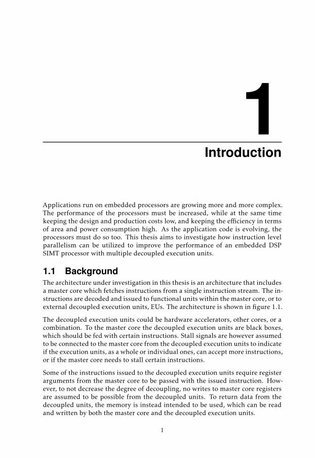
1.1 BackgroundThe architecture under investigation in this thesis is an architecture that includesa master core which fetches instructions from a single instruction stream. The in-structions are decoded and issued to functional units within the master core, or toexternal decoupled execution units, EUs. The architecture is shown in figure 1.1.
The decoupled execution units could be hardware accelerators, other cores, or acombination. To the master core the decoupled execution units are black boxes,which should be fed with certain instructions. Stall signals are however assumedto be connected to the master core from the decoupled execution units to indicateif the execution units, as a whole or individual ones, can accept more instructions,or if the master core needs to stall certain instructions.
Some of the instructions issued to the decoupled execution units require registerarguments from the master core to be passed with the issued instruction. How-ever, to not decrease the degree of decoupling, no writes to master core registersare assumed to be possible from the decoupled units. To return data from thedecoupled units, the memory is instead intended to be used, which can be readand written by both the master core and the decoupled execution units.
1

2 1 Introduction
Master core
IM
Decoder & Issuer
FU
Decoupled EUs
Stall
Figure 1.1: The architecture under investigation. The master core fetchesinstructions from the instruction memory, IM, and issues them to functionalunits, FUs, or to decoupled execution units, EUs.
The decoupled execution units could have instruction queues to allow for moreinstructions to be issued to them before needing to stall further issues, but couldalso be fully occupied by a single issued instruction. Both cases will be handledin the same way by the master core, and the master core requires no informationabout the internal architecture or functionality of the decoupled execution units,other than what instructions to issue where.
The decoupled execution units would typically be introduced to solve some spe-cialized task not possible to solve, or not possible to solve as efficiently, by themaster core. They are also used to increase parallel execution.
1.1.1 Processor tasksThe processor under investigation is one of many processors in a mobile phoneapplication. The tasks of the processor includes both digital signal processing,DSP, and control tasks. Much of the DSP tasks will be issued to decoupled ex-ecution units for faster handling, while all control tasks will be handled by themaster core. Some smaller DSP tasks will still be handled by the master core, soDSP instruction support in the master core is required.
1.1.2 The BBP2 processorOne processor which is organized as described above, with a master core andmultiple decoupled execution units, is the BBP2 processor [8], refined from theBBP1 processor [12]. The BBP2 processor has one controller core, acting as a

1.2 Problem definition 3
master core. The BBP2 also has two decoupled SIMD execution units: One 4-waycomplex MAC (CMAC) and one 4-way complex ALU (CALU). The controller coreissues instructions to the CMAC and the CALU. Their network connections arealso configured by the controller core. Further, the BBP2 has several acceleratorsdesigned to solve specific baseband processing tasks.
The BBP2 processor is classified by Nilsson [8] as a Single Instruction stream-Multiple Tasks, SIMT, architecture. RISC instructions executed by the controllercore are mixed with vector instructions issued to and executed by the SIMD ex-ecution units. The vector instructions operate on large data sets for a numberof cycles, thus providing the notion of the processor doing multiple tasks at thesame time. This provides parallelism and a higher performance without havingto issue multiple instructions each cycle, therein simplifying the control path.
1.2 Problem definitionThe SIMT execution model describes how parallelism is exploited over the mastercore functional units and the decoupled execution units. In its basic form only asingle instruction is issued every cycle, either to a master core functional unit orto a decoupled execution unit. However, if the control of the decoupled executionunits becomes fine-grained, meaning that the decoupled execution units needfrequent instructions to not be starved, or if the control burden of the master corebecomes sufficiently high, the fetching and decoding of instructions can becomethe bottleneck of the system. In order to keep all functional units and decoupledexecution units busy, one needs to consider methods for how to parallelize theinstruction fetch and decode process.
Traditional parallel fetch and decode methods such as superscalar and VLIW arepossible methods to use to improve instruction throughput and it is of high inter-est to evaluate the benefits and drawbacks of these methods for the SIMT archi-tecture. Also, it is of interest to investigate what additional improvements can bedone considering that the fetch and decode pipeline in the master core can avoiddeep inspection of instructions for decoupled execution units, as long as it candecide the destination unit.
The thesis will try to answer the following two questions:
• What are the benefits and drawbacks of a superscalar architecture and aVLIW architecture for a processor with a combination of DSP and controltasks?
• How can consecutive instructions meant for a decoupled execution unit bepackaged and issued to increase the performance of the processor?
1.3 Thesis outlineSome classifications and concepts central to the thesis is described in chapter 2.Chapter 3 presents and discusses important aspects of the master core architec-ture design. The choice of master core architectures, their RTL implementations

4 1 Introduction
and the synthesis and benchmark results are presented in chapter 4. Chapter 5presents and discusses different aspects relating to issuing to decoupled execu-tion units. Conclusions and possible future work is given in chapter 6.

2Theory
This chapter will describe some concepts central to the work done. Some im-portant computer architectures will be described, and the concept of conflicts isdefined. A general description of a digital signal processor is also given.
2.1 Computer architecturesThis section will describe some computer architectures and organizations centralto digital signal processors and the work carried out.
2.1.1 Single Instruction stream-Single Data stream architectureA very common architecture is the Single Instruction stream-Single Data stream,SISD, architecture, a classification described in Flynn’s Taxonomy [4]. A proces-sor with a SISD architecture operates on a single instruction stream, fetching theinstructions in order. All instructions operate on a single piece of data, and eventhough this could for example be multiple registers as different operands, no vec-tor operations are performed.
There are many variants of the SISD architecture, both throughout history andtoday.
2.1.2 Scalar processorA scalar processor is the simplest variant of the SISD architecture. In a scalar pro-cessor, no instruction level parallelism is exploited, only fetching one instructionat a time, decoding it, and then executing it. Most scalar processors do howeverhave a pipeline to increase the throughput of instructions.
The advantages of a scalar processor is that it is quite easy to design and compilecode for. However, as it exploits no parallelism, most programs operate much
5

6 2 Theory
slower on a scalar processor than on another type of processor.
2.1.3 Superscalar processorA superscalar processor is a more complex type of processor than a scalar pro-cessor, but is still classified as a variant of the SISD architecture. A superscalarprocessor tries to dynamically schedule instructions to be executed in parallel.It still operates on a single instruction stream, but fetches multiple instructionseach clock cycle and then evaluates in the decode stage if they can be executedat the same time. A number of possible conflicts, described in section 2.2, canprevent instructions from being executed at the same time.
2.1.4 Very Long Instruction Word processorAnother type of processor which utilizes parallelism is a Very Long InstructionWord, VLIW, processor. A VLIW processor relies on a compiler to statically deter-mine what instructions can be executed in parallel. A VLIW processor still oper-ates on a single instruction stream, but the stream consists of larger instructionpackets packaged by the compiler. This means that no conflict checks betweeninstructions within a packet are needed at runtime, but instead demands moreof the compiler, which needs to account for the same conflicts as the superscalarprocessor.
2.1.5 Single Instruction stream-Multiple Data streamsAnother architecture classification described in Flynn’s Taxonomy [4] is the Sin-gle Instruction stream-Multiple Data streams, SIMD, architecture. A processorwith a SIMD architecture operates on a single instruction stream, fetching in-structions in order, but then using each instruction for multiple data streams.This means that every operation can operate on multiple pieces of data, allowingfor fast processing of large amounts of data without increasing the code size.
2.1.6 Vector processorA common kind of processor with a SIMD architecture is the vector processor. Avector processor typically have vector registers, often in combination with scalarregisters. Vector registers can hold multiple pieces of data. Instructions can fetchdata to vector registers quickly, and can generally operate on all pieces of data ina vector register at the same time.
Vector processors are very common in DSP applications due to the fact that theycan process large amounts of data quickly, and most DSP operations should beperformed on a fast stream of data.
2.2 ConflictsA conflict is in this thesis defined as a conflict between instructions, where forsome reason an instruction cannot be executed due to the execution of anotherinstruction.
There are three kinds of conflicts that can arise [1], [10], namely data conflicts,structural conflicts and control conflicts. All three are described below.

2.2 Conflicts 7
1 ADD R0, R1, R2 ; R0 + R1 -> R22 SUB R2, 0x1, R3 ; R2 - 1 -> R33 AND R4, R1, R2 ; R4 & R1 -> R2
Listing 2.1: Instructions with data dependencies.
2.2.1 Data conflictA data conflict can occur when there are data dependencies between instruc-tions. Data dependencies can be of three different kinds – true dependency, anti-dependency and output dependency. A true dependency (or read after write,RAW) occurs when an instruction requires data produced by an earlier instruc-tion. An anti-dependency (or write after read, WAR) occurs when an instructionoverwrites a variable read by an earlier instruction. An output dependency (orwrite after write, WAW) occurs when an instruction overwrites a variable writtenby an earlier instruction.
Listing 2.1 show three instructions which exhibit all three different data depen-dencies. Instruction 2 has a true data dependency on instruction 1, as it re-quires the result produced by instruction 1 as input. Instruction 2 has an anti-dependency on instruction 3, as instruction 3 will overwrite R2 which is read byinstruction 2. Instruction 3 has an output dependency on instruction 1, as bothof them write to R2.
A true data dependency cannot be removed, but can in some cases be mitigatedor avoided by reordering the instructions to allow for enough time between twoinstructions with a true data dependency for the first instruction to finish beforethe second instruction is started.
Output and anti-dependencies can be removed by using more registers, wherethe second occurrence of a destination register is changed to another, unusedregister. However, all following instructions that read that register also needto be changed to instead read the new register. This can be done by the com-piler, or by the processor at run time. When done by the processor it is generallyreferred to as register renaming. As an example, in listing 2.1 above, R2 in in-struction 3 could for instance be renamed to another register, thus removing theanti-dependency and the output dependency.
2.2.2 Structural conflictA structural conflict can occur when multiple instructions want to use the sameresource. To decrease the risk of a structural conflict, extra copies of resourcescan be added. Resources can here be for example ALUs, but also connections likeregister file ports. By adding extra copies of resources, instructions that wouldnormally cause a structural conflict can be executed without a conflict, by usingdifferent instances of the resource.
2.2.3 Control conflictA control conflict occurs when branching and the target address is unknown un-til the branch is executed. A control conflict also occurs when a branch is condi-

8 2 Theory
tional, i.e. when it is unknown beforehand whether or not the branch should betaken. When a control conflict occurs it is uncertain which instructions should beexecuted, and thus the processor will need to wait until the conflict is resolved.
2.3 Digital Signal ProcessorA Digital Signal Processor, DSP, is a processor specifically designed to solve dig-ital signal processing tasks. The degree of specialization can vary, and DSPs canbe divided into two main groups – Application Specific Instruction set ProcessorDSPs, ASIP DSPs, and General Purpose DSPs, GP-DSPs. ASIP DSPs are more spe-cialized than GP-DSPs, but both are more specialized than a General Purpose Pro-cessor, GPP. The specialization comes from the knowledge that DSPs will only beused for certain applications, and the architecture can be optimized accordingly.The more specific the application, the more optimizations can be done.
The nature of digital signal processing tasks is very much kept in mind when de-signing a DSP. For example, a common operation in DSP applications is the MAC(multiply-accumulate) operation, and much can be gained from adding specialMAC units and optimizing them. Other special instructions and accelerators canalso be added to a DSP.
DSPs can have varied architectures but are generally RISC-based with CISC en-hancements [7]. This means that most instructions are typically single-cycle in-structions which operate solely on the register file, or between the memory andthe register file (load/store). The CISC enhancements can for example be specialinstructions with extra hardware for convolution, division or multiplication. Inaddition, the architecture is typically some variant of SISD or SIMD.
Throughout this thesis the acronym DSP will be used interchangeably as meaningDigital Signal Processor or Digital Signal Processing.

3Master core architecture design
This chapter presents and discusses some architecture design choices which canimpact the performance and design- and production costs of the master core.
Given the overall architecture and the tasks described in section 1.1, the mastercore is essential to the performance of the complete system. The master core han-dles all control instructions and issues all instructions to the decoupled executionunits. This means that the master core could end up limiting the performance ifit is not performing well enough. Therefore it is of interest to investigate how theperformance of the master core is impacted by the choice of architecture.
3.1 Architecture design choicesA performance that is better than what a scalar processor generally can provide iswanted. There are multiple different architectures that could provide this. If themajority of the tasks are DSP related, a SIMD architecture might be preferable,to quickly process large amounts of data. However, as described in section 1.1.1,the tasks run on the master core is of both DSP and control nature. With morecontrol tasks present, a SIMD architecture might be hard to fully utilize. Insteada SISD architecture might be better. This is one reason why superscalar and VLIWarchitectures are of most interest. However, both of these can look quite different,and thus superscalar and VLIW design choices will be investigated.
3.1.1 In-order vs. out-of-order superscalarWhen designing a superscalar processor one must decide if instructions alwaysshould be executed in-order, or if one can allow for out-of-order execution. Out-of-order execution means that a number of instructions are examined and pos-sibly reordered to get less stalls due to conflicts. This is done in hardware atruntime.
9

10 3 Master core architecture design
Out-of-order execution can lead to more optimized code execution, with feweridle execution units and less stalls due to conflicts. However, implementing out-of-order execution adds complexity to the hardware, both in terms of extra areaand power needed for analysis, and in terms of development and design. Imple-menting out-of-order execution is not trivial, and introduces new problems.
One problem regards interrupts. When saving the state of the processor beforerunning the interrupt one usually saves the address of the instruction to return towhen the interrupt is done. When executing instructions out-of-order that is notenough, as more information about which instructions that have been executedalready is needed, to not miss any instructions and to not execute any instructiontwice. A similar argument can be made for exceptions.
The window size of an out-of-order processor determines how much the perfor-mance is increased. The window size is the number of instructions that are an-alyzed at the same time before reordering. This does not have to be the sameas how many instructions can be issued at the same time, the window size islikely larger. The larger the window size, the better the chances are for findingindependent instructions that can be moved. But as the window size goes up,the complexity of the hardware increases rapidly, as the number of dependencychecks grows exponentially with the window size.
An in-order processor will never reorder instructions, but preserve the order ofinstructions in the program. If a conflict is detected, the instruction with theconflict and all following instructions are stalled until the conflict is resolved.This means that there will be more stalls overall, but less logic will be required.
The performance of an in-order processor is heavily dependent on the compiler.If the compiler takes into account how wide the processor is, what functionalunits are available, and how much latency each instruction has, it can reorderthe instructions at compile time, just as the out-of-order processor would do atruntime. This will increase the performance significantly, and give similar perfor-mance as an out-of-order processor without the added hardware, but it requiresan advanced compiler.
As an example for a 2-way, in-order, superscalar processor one can examine thecode in listing 3.1. If we assume that all instructions only have a latency of 1cycle, meaning the result can be used in the following cycle, we can see that theordering is poor, due to the fact that instruction 3 is dependent on instruction 2,which is dependent on instruction 1. The same goes for instruction 6, 5 and 4.This means that the processor will have to execute the instructions as in table 3.1,where only one cycle executes two instructions in parallel. This can be improvedby reordering the instructions as in listing 3.2. This new instruction order spacesout the dependencies, allowing for an execution as in table 3.2, where all cyclesexecute two instructions in parallel.
The reordering example above could likely be solved by an out-of-order proces-sor during runtime, and could for an in-order processor be done at compile time.However, if the latencies of the instructions were longer it would be harder. More

3.1 Architecture design choices 11
1 LDI 0x9, R0 ; 9 -> R02 ADD R0, R1, R2 ; R0 + R1 -> R23 SUB R2, 0x1, R3 ; R2 - 1 -> R34 LDI 0x5, R4 ; 5 -> R45 ADD R4, R1, R5 ; R4 + R1 -> R56 SUB R5, 0x1, R6 ; R5 - 1 -> R6
Listing 3.1: Poorly ordered instructions.
Table 3.1: Execution of poorly ordered instructions in listing 3.1 in a 2-way,in-order superscalar processor.
Cycle Execute slot 0 Execute slot 1 Comment
1 LDI 0x9, R0 – R0 data conflict in slot 1
2 ADD R0, R1, R2 – R2 data conflict in slot 1
3 SUB R2, 0x1, R3 LDI 0x5, R4
4 ADD R4, R1, R5 – R5 data conflict in slot 1
5 SUB R5, 0x1, R6 –
1 LDI 0x9, R0 ; 9 -> R02 LDI 0x5, R4 ; 5 -> R43 ADD R0, R1, R2 ; R0 + R1 -> R24 ADD R4, R1, R5 ; R4 + R1 -> R55 SUB R2, 0x1, R3 ; R2 - 1 -> R36 SUB R5, 0x1, R6 ; R5 - 1 -> R6
Listing 3.2: Well ordered instructions.
Table 3.2: Execution of well ordered instructions in listing 3.2 in a 2-way,in-order superscalar processor.
Cycle Execute slot 0 Execute slot 1 Comment
1 LDI 0x9, R0 LDI 0x5, R4
2 ADD R0, R1, R2 ADD R4, R1, R5
3 SUB R2, 0x1, R3 SUB R5, 0x1, R6

12 3 Master core architecture design
instructions would have to be moved to space out the dependencies further. Aformulae for the number of instructions needed between two dependent instruc-tions (true dependency) given the latency of the first instruction and the numberof ways in the processor can be formulated.
Theorem 3.1. The number of instructions required between two instructions,where the second instruction have a true data dependency on the first instruction,to guarantee no stalls are generated due to data dependencies is
ClatencyPways − 1
where Clatency is the latency of the first instruction, i.e. the number of cycles be-fore the result can be used (counting the starting cycle), and Pways is the numberof ways in the processor.
A compiler for an in-order superscalar processor should ideally try to use thiswhen reordering the instructions to produce optimal code. It should also be usedby an out-of-order processor when reordering the instructions at runtime. How-ever, it should be noted that by spacing out dependencies, the number of registersrequired might increase. For example, looking back at the code in listing 3.1 onecould reuse some of the registers, reducing the number of registers required with-out increasing the execution time. The same could not be done in listing 3.2.
So, the choice between in-order and out-of-order comes down to four things:
• What performance is required?
• What production cost is acceptable?
• What design cost is acceptable?
• Is an advanced compiler available or possible to design?
These questions need to be answered when making the decision. As every ap-plication has different properties the questions have no universal answer, andtherefore need to be examined in each case separately.
3.1.2 Number of superscalar waysAnother choice to make when designing a superscalar processor is how manyways the processor should have. A way is here defined as a slot in which aninstruction can be issued. A 4-way processor can for example issue a maximum of4 instructions per cycle, but often issues less than 4 instructions due to conflicts.
The ways can be homogenous or heterogenous in terms of what instructions canbe issued in each way, most likely due to differences in what functional units areavailable in each way. However, the ways do not have to be defined as separateslots or paths entirely, one could instead see the number of ways as how manyinstructions that can be decoded and issued to functional units each cycle. Inthis case the functional units can be seen as in a pool which the ways can pick

3.1 Architecture design choices 13
from. This gives more freedom when assigning instructions to ways, but requiresextra muxing of signals when choosing the inputs to the functional units instead.
Most likely there will be more ways than functional units of each type. For ex-ample, a 4-way processor might have 4 arithmetic units, but only 2 multipliers,meaning that the heterogeneity comes from the fact that 4 arithmetic instruc-tions could possibly be issued at the same time, but not 4 multiplications. For ahomogenous 4-way processor there would be no such restrictions, meaning thatthe processor would need 4 units of each function.
As the possible performance increases with the number of ways one might thinkthat more is always better. But extra ways come at a cost. For each added way,more dependency checks are required and the amount grows exponentially withthe number of ways. The number of functional units might also have to be in-creased to actually get better performance. Both the extra checks and functionalunits will increase the area and power consumption, as well as increasing thedesign and verification cost. Therefore one needs to think about if the possibleextra performance is required and/or can be afforded.
As more ways and dependency checks are added, more and more timing con-straints are introduced. This is in some ways a worse and more complex problem.The extra constraints can reduce the possible clock frequency of the design, thuslowering the number of instructions that can be executed per second. The lowerclock frequency may still be worth it, if the overall performance is increasedthanks to the extra ways. If not, no extra ways should be added, unless other im-provements also are made. To decrease the timing constraints one can introduceextra pipeline steps. This can allow for a much higher clock frequency, but will in-troduce other problems. Extra pipeline steps will make the design more complex,resulting in a higher design and verification cost. Extra steps will also introducea higher pipeline latency, meaning it will take longer to fill the pipeline, whichfor example needs to be done if a branching instruction has caused the pipelineto be flushed.
Another thing to consider is that more ways do not always result in an increase inperformance. A superscalar processor relies on the instruction level parallelismof the program. If there are not enough instructions in the program that canbe run in parallel, extra ways might be idle most of the time. This means thatthe nature of the application and specific program which is intended to be rundetermines whether or not extra ways will increase performance.
So the choice of the number of ways and if they should be homogenous or het-erogenous comes down to similar questions as in section 3.1.1, namely:
• What performance is required?
• What production cost is acceptable?
• What design cost is acceptable?
• How parallel is the application?

14 3 Master core architecture design
Just as in section 3.1.1, these questions are answered differently for each applica-tion, and need to be reflected on separately in each case.
3.1.3 Memory and code sizeIn many modern embedded processors, on-chip memories account for more thanhalf of the core chip area. For example, the BBP2 processor has a memory areaof about 55 % of the core area [8]. Furthermore, memory access often account formore than half [5], or even as much as 70 % [3], of the total power consumption ofthe chip. These numbers indicate that reducing the size of memories can greatlyreduce the total chip area as well as reducing the power consumption.
Memories can be shared by both instructions and data, but can also be split intodata memories and program memories. If the code size of the programs runningon the processor is reduced, the size of the program memory, or the combinedmemory, can also be reduced. One way to reduce the code size can be to optimizethe instruction encoding. Another way is to alter the application code and thecompiler to aim for a smaller code size.
3.1.4 VLIW instruction encodingWhen designing a VLIW processor the instruction encoding can greatly impactthe code size and also somewhat the decoding complexity, due to the fact that theinstruction parallelism needs to be explicitly defined in the VLIW instruction.Therefore one should carefully consider the instruction encoding.
Fixed instruction lengthIn some sense the simplest approach is to have a VLIW instruction word that haveone fixed sized slot for every functional unit. This could look like in figure 3.1a,if the processor has 2 ALUs, 1 LSU (load/store unit) and 1 branch unit. If afunctional unit cannot be used, due to lack of a certain type of instruction or dueto conflicts, a NOP is inserted in that slot instead. This encoding is very fast todecode, as no muxing between the slots to different functional units is required.However, in a more complex processor there will likely be many more functionalunits such as multipliers, dividers and additional ALUs and LSUs. In this case theVLIW instruction would become extremely long, and most slots would be empty(with NOPs inserted) which would make the code size very large. A grouping offunctional units could then be done, with one slot for each group. This wouldstill be quite efficient as a functional unit will always get its inputs from the sameslot, but this would require more of the compiler when placing instructions intothe slots, unless all functional unit types are available for each slot.
All functional units can also be shared by all slots. In that case the compilerdo not have to place instructions into any specific slot, resulting in unspecific,general slots. For total freedom all types of functional units would have as manyinstances as there are slots, but that is often not preferred as it can be expensiveand would not necessarily increase performance considerably. Instead one canhave fewer functional units and mux between the different slots depending onthe instructions in them. This could then look as in figure 3.1b for a 4-way VLIWprocessor. In this case the slots still have a fixed size. The fixed size allows for

3.1 Architecture design choices 15
ALU slot 0 ALU slot 1 LSU slot BRANCH slot
(a) VLIW encoding with fixed slot size, fixed number of slotsand specific slots.
Slot 0 Slot 1 Slot 2 Slot 3
(b) VLIW encoding with fixed slot size and fixed number ofslots.
Number ofslots Slot 0 Slot 1 Slot 2
(c) VLIW encoding with fixed slot size, variable number ofslots, and a field for number of slots.
Figure 3.1: Three possible VLIW encodings with fixed slot size.
simpler encoding and decoding as all slots can be decoded at the same time.
The encoding in figure 3.1b will still generally have quite bad code size due toadded NOPs. To get rid of the NOPS one could instead have a variable numberof slots, and instead of adding a NOP when not being able to populate a slot, theslot can be removed. But the information about which instructions that can berun in parallel still needs to be kept somehow. One way to solve it would be as infigure 3.1c, where an extra field is added as a header to the VLIW instruction. Theheader holds how many slots are in the VLIW instruction. This introduces someextra checks when decoding but can decrease the code size drastically. An upperlimit on the number of slots would be needed, as the processor will still have anupper limit on how many instructions it can decode at a time. A lower limit canbe imposed (most likely 1), but is not necessary. Depending on the upper limit, alower limit can possibly save a bit in the header as a length of 0 for example donot have to be possible. If no lower limit is imposed, the length of 0 can insteadbe used to make the processor skip one cycle. This could be the same as insertingNOPs in all slots. Depending on how often this is used it could save more overallcode size than the possibly saved bit in the header.
Variable instruction lengthAll encodings described so far have a fixed slot size. A fixed slot size can producea faster and smaller decoder thanks to the fact that the start position of eachinstruction is known, as it means that all slots can be decoded in parallel andthat no large amount of muxing is required. However, having all instructionsbeing the same length produces an unnecessarily large code size. If one allowsfor instructions of different lengths the code size can be decreased.
Given an instruction set, an application program and the goal to minimize theoverall code size, more common instructions will get shorter encodings, and moreuncommon will get longer ones. Further optimizations can be done by alteringthe instruction set, by adding special variations of some instructions and giving

16 3 Master core architecture design
Slot 0 Slot 1 Slot 2 Slot 3
Size Operation
(a) VLIW encoding with variable slot size with size informa-tion in slots, and fixed number of slots.
Slot starts
Slot 0start
Slot 1start
Slot 2start
Slot 3start
Slot 0 Slot 1 Slot 2 Slot 3
(b) VLIW encoding with variable slot size, fixed number ofslots, and a field for start position of each slot.
Number ofslots
Size Operation
Slot 0 Slot 1 Slot 2
(c) VLIW encoding with variable slot size with size informa-tion in slots, variable number of slots, and a field for numberof slots.
Slot starts
Slot 0start
Slot 1start
Slot 2start
Slot 0 Slot 1 Slot 2Number ofslots
(d) VLIW encoding with variable slot size, variable numberof slots, a field for number of slots, and a field for start posi-tions of each slot.
Figure 3.2: Four possible VLIW encodings with variable slot size.

3.1 Architecture design choices 17
them their own encoding. For example, a very common instruction in most pro-grams is to push a register to the stack. This is in reality a store instructionwith the address specified in the stack pointer register. So, a push instructioncould be added where only the source register needs to be specified, and wherethe stack pointer is always used as the address pointer. Such common, special-ized instructions can decrease code size further, as the new instruction can get ashorter encoding. Some restrictions can be imposed when optimizing the instruc-tion lengths. A common restriction is to have the lengths be a variable number offull bytes, and possibly disallowing certain number of bytes. This will of coursedecrease the potential gain of the optimization but can make fetch and decodeeasier.
A possible encoding with variable instruction length is shown in figure 3.2a. Herethe number of slots is fixed but the slots have variable length, as long as theinstructions they hold. The size of each instruction is located as a header foreach instruction. The drawback of variable-length instructions becomes apparenthere. All four slots should be decoded and run in parallel but that is not possibleas the start positions of the slots are unknown. To find the second instructionone must first determine the size of the first. For the third instruction, the sizeof both the first and the second instruction must be extracted before the start ofthe third instruction can be determined. This problem grows with the number ofslots.
A way to decrease the impact of the unknown start positions is to encode theVLIW instruction as in figure 3.2b, which has a header with the start positions ofall slots. If the slot start position fields have a fixed size, the start positions canbe read in parallel, decreasing the time needed to determine the location of everyinstruction. The instructions can then also be read in parallel. Information aboutthe size of each instruction can still be placed in the instruction encoding as infigure 3.2a, as this can simplify the encoding.
The encodings in figure 3.2a and figure 3.2b both suffer from the same problemsas the fixed-length instruction encodings with a fixed number of slots, that NOPsoften needs to be inserted. However, the impact will not be as large as for thefixed-length instructions due to the fact that NOP can have a short encoding.Even so, the NOPs can be removed, resulting in an encoding as in figure 3.2cwhere the number of slots is variable. Like for the fixed-length instructions, afield with information about the number of slots present is added. The problemwith the slot start positions arises again. Therefore an encoding like in figure 3.2dcan be produced, where once again the slot start positions are specified in a sep-arate field. The number of slots present can dictate the length of the slot startpositions field, or not if one wants to keep the logic simple, as the start positionthen would have to once again be calculated, but can at least be done so in paral-lel for the different slots.
VariationsVariations to the encodings above, as well as completely different ones, can ofcourse be used. The ones mentioned are in no way the only ones, nor are they

18 3 Master core architecture design
necessarily the best ones, merely a natural evolution described.
3.1.5 Superscalar instruction encodingWhen designing a superscalar processor it is important to consider the instruc-tion encoding, just like for a VLIW processor described in section 3.1.4. Thedifference between superscalar code and VLIW code is that there is no explicitparallelism in the superscalar code, the possibility to run instructions in parallelis up to the processor to examine. Therefore superscalar code only consists ofindividual instructions.
A simple instruction encoding is shown in figure 3.3a. Here fixed-length instruc-tions are used. A superscalar processor wants to fetch and examine multiple in-structions at once. A fixed-length instruction encoding allows for easy fetch andfast decode thanks to the known start position of each instruction, and multipleinstructions can be decoded in parallel. Compared to fixed-length VLIW instruc-tion encodings, superscalar code is typically much smaller, especially for VLIWencodings where NOPs need to be inserted. However, superscalar code size canbe reduced as well. This can for example be done by allowing variable-lengthinstructions.
Figure 3.3b shows a variable-length instruction encoding with the size of eachinstruction specified at the start of the instruction. Other possibilities to deter-mine the size are of course possible, such as having the last bit of every bytedetermining if the next byte is a new instruction or is a part of the previous in-struction. In any case, the variable size can decrease the overall code size, justlike for VLIW, where common instructions get shorter encodings. Specializedcommon instructions can further decrease the code size. However, just like forVLIW, the unknown instruction length is problematic when trying to decode mul-tiple instructions at once. The size of the first instruction needs to be determinedbefore the position of the second instruction can be known. This introduces ex-tra timing constraints. Some things can however be done to mitigate this. Onepossibility is to decode all possible start positions and then choosing the correctones once known. This is effective but can be very expensive in terms of area andpower cost.
One variable-length instruction encoding developed specifically for parallel fetchand decode is the Heads and Tails, HAT, encoding [9]. HAT-encoding splits allinstructions into a fixed-length head and a variable-length tail. The instructionsare then packaged into bundles. If a cache is used, the width of the bundlesshould be the same as the width of the cache lines. Two example bundles canbe seen in figure 3.4. First in the bundle is a field specifying the number ofinstructions in the bundle minus one, then comes the fixed-length heads followedby potentially an empty region and then the tails in reverse order, with the firsttail starting at the last bit of the bundle. Instructions are bundled as many ascan fit or until the number of instructions field is saturated. Restrictions on thelength of the tails can be set, and one can allow some instructions without tails,or not. Due to the variable length of the instructions it is not always possibleto perfectly fit them in a bundle, instead a region between the heads and the

3.2 Superscalar vs. VLIW 19
Instr. 0 Instr. 1 Instr. 2 Instr. 3
(a) Superscalar instruction encoding with fixed-length in-structions.
Instr. 0 Instr. 1 Instr. 2 Instr. 3
Size Operation
(b) Superscalar instruction encoding with variable-lengthinstructions.
Figure 3.3: Two possible superscalar instruction encodings.
3 H0 H1 H2 H3 T3 T2 T1 T0
4 H0 H1 H2 H3 T4 T2 T1 T0H4
Figure 3.4: Heads and Tails-encoding examples. H# are the heads of theinstructions, and T# are the tails. The starting number is the number ofinstructions in the bundle minus one. The grey area is unused.
tails can be left unused. During decoding, each head location is known and eachhead holds information about the length of its tail. This means that all previousinstructions in the bundle still needs to be analyzed before the next, but since alllength information is available in the fixed positioned heads it is not as complex.This potentially allows for more instructions to be analyzed at the same timewithout introducing very restrictive timings. However, some empty regions willbe introduced, increasing the overall code size somewhat.
3.2 Superscalar vs. VLIWSuperscalar and VLIW processors have both generally better performance thana scalar processor, but costs more to design and produce. They do not howeveralways perform better, and they have some particularities which makes them per-form differently in certain cases. These particularities should be kept in mindwhen choosing between a superscalar and VLIW processor. Some of the particu-larities are described below.
3.2.1 Issue and stalling of instructions with uncertain latenciesData dependency is one of the main reasons for stalling an instruction. One verycommon situation in all applications are loads from memory followed by opera-tions on the loaded data. The operation instructions have a data dependency onthe load instructions and might therefore result in stalls.

20 3 Master core architecture design
1 LOAD [R0], R1 ; [R0] -> R12 ADD R2, 0x4, R2 ; R2 + 4 -> R23 LOAD [R2], R3 ; [R2] -> R34 ADD R1, R4, R5 ; R1 + R4 -> R55 CMP 0, R3 ; 0 - R3
Listing 3.3: Instruction sequence with high potential for stalling due to un-certain load latencies.
Table 3.3: Execution of instructions in listing 3.3 in an in-order scalar pro-cessor.
Cycle Execute slot Comment
1 LOAD [R0], R1
2 ADD R2, 0x4, R2
3 LOAD [R2], R3
4 stall R1 data conflict...
...20 stall R1 data conflict
21 ADD R1, R4, R5 Load to R1 done
22 stall R3 data conflict
23 CMP 0, R3 Load to R3 done
Table 3.4: Execution of instructions in listing 3.3 in a 2-way, in-order super-scalar processor.
Cycle Execute slot 0 Execute slot 1 Comment
1 LOAD [R0], R1 ADD R2, 0x4, R2
2 LOAD [R2], R3 – R1 data conflict in slot 1
3 stall – R1 data conflict...
...20 stall – R1 data conflict
21 ADD R1, R4, R5 – Load to R1 done, but not to R3
22 CMP 0, R3 – Load to R3 done

3.2 Superscalar vs. VLIW 21
In order to mitigate the effect of load latencies, the instructions can if possible bereordered to allow for independent instructions to be executed while waiting forthe load to finish. If the load latency is known at compile time this can be quiteeffective. However, if the load latency is unknown, or uncertain, the compilerwill not know how to schedule the instructions optimally. An unknown loadlatency can arise in a processor with a memory hierarchy, which are present inmost processors, where for example a cache or multiple memories at differentlatencies are used. In the unknown case, the compiler must fall back to a defaultlatency.
Another common situation in most applications is that there is a load instructionwith the address calculated by an earlier arithmetic instruction. This in itself isnot too bad, but in combination with the previously mentioned load situationthings can get problematic.
Listing 3.3 is an example of the situation described above. Instruction 4 is de-pendent on the load in instruction 1, and instruction 3 needs the result frominstruction 2 as an address. Finally, instruction 5 needs the result from the loadin instruction 3. During scheduling, the compiler in this example assumed thatthe latency of both loads is 1 cycle, but will in reality be 20 cycles. This discrep-ancy could come from the compiler assuming that the values are cached, wherea load from the cache might take 1 cycle, but where a cache miss might take 20cycles. Arithmetic operations have a latency of 1 cycle.
When executing the instructions on an in-order scalar processor they will executeas in table 3.3. Due to the longer than anticipated load latencies, multiple stallcycles will be introduced. In this example processor, multiple loads can be activeat the same time. The total execution time will be 23 cycles.
The same program executed on a 2-way, in-order superscalar processor will exe-cute as in table 3.4. This will look mostly like the scalar processor, only movingone addition, resulting in a total execution time of 22 cycles.
If the instructions in listing 3.3 are recompiled for a 2-way VLIW processor, us-ing the same scheduling rules, the instruction sequence in listing 3.4 might beproduced. When executing this on a VLIW processor which also have the 20 cy-cle load latency it will look as in table 3.5. Due to the processor not being able toseparate the slots in the VLIW instructions, the second load cannot be executeduntil the data dependency in the addition is resolved. This results in no overlapof the load latencies, which in turn results in a total execution time of 42 cycles.
If the load latencies would have been 1 cycle as assumed by the compiler, therewould be no big difference between the superscalar and VLIW processors. Butwhen the load latencies are unknown or uncertain, problems like these can beintroduced, and the scheduling becomes more difficult.
3.2.2 Instruction packaging around branch targetsBranching can in many situations prove to be problematic. One such problem isthat a branch instruction will affect the packaging of VLIW instructions around

22 3 Master core architecture design
1 LOAD [R0], R1 || ADD R2, 0x4, R22 LOAD [R2], R3 || ADD R1, R4, R53 CMP 0, R3
Listing 3.4: VLIW instructions with high potential for stalling due to uncer-tain load latencies.
Table 3.5: Execution of instructions in listing 3.4 in a 2-way VLIW processor.
Cycle Execute slot 0 Execute slot 1 Comment
1 LOAD [R0], R1 ADD R2, 0x4, R2
2 stall – R1 data conflict...
...20 stall – R1 data conflict
21 LOAD [R2], R3 ADD R1, R4, R5 Load to R1 done
22 stall – R3 data conflict...
...41 stall – R3 data conflict
42 CMP 0, R3 – Load to R3 done
the target address. VLIW instructions are statically defined by the compiler andexpress explicit parallelism. If the execution of an instruction is uncertain it mustoften be separated from other instructions.
An example of when this behavior exhibits itself can be seen in listing 3.5. Inthis code there are two conditional branch instructions with target addresses 13and 16 which both lies in a region with independent instructions, which ideallyshould be run as much in parallel as possible. When run on a superscalar proces-sor this will not be an issue since the instructions are scheduled dynamically. Butthere will be an issue for a VLIW processor. The VLIW compiler needs to takethe target addresses into account when packaging the instructions, because of thenote that a branch cannot end up in the middle of a VLIW instruction, only at thestart. For the examined instruction sequence, the equivalent VLIW code wouldbe as in listing 3.6. One can see that some instructions remain by themselves,even though no dependencies are present, as the target addresses needs to be atthe start of an VLIW instruction.
The instruction packaging around branch targets is a problem both during com-pilation and when executing the code. A VLIW compiler needs to adjust VLIWinstructions to fit branch targets, making the compiler slightly more complex.When executing the code, the separation of VLIW instructions will cause fewerinstructions to be run in parallel, thus increasing the execution time.
A way to relieve the need to separate instructions around branch targets wouldbe to specify in the branch instruction what slots of the target VLIW instruction

3.2 Superscalar vs. VLIW 23
10 LDI 0, R011 LDI 1, R112 LDI 2, R213 LDI 3, R314 LDI 4, R415 LDI 5, R516 LDI 6, R617 LDI 7, R7
...40 BEQ 13
...53 BEQ 16
Listing 3.5: Instruction sequence with branch targets.
10 LDI 0, R0 || LDI 1, R111 LDI 2, R212 LDI 3, R3 || LDI 4, R413 LDI 5, R514 LDI 6, R6 || LDI 7, R7
...35 BEQ 12
...47 BEQ 14
Listing 3.6: VLIW instruction sequence with branch targets.
should be executed. This means that the compiler would alter the branch in-struction depending on the target location instead of separating the instructionat the target. This in turn means that the code might execute faster, as more in-structions can be executed in parallel when only passing by a branch target. Thecomplexity of the compiler will be roughly the same, but the complexity of eachbranch instruction will be increased, which the hardware must account for. Thiscould prove to be costly.


4Master core implementation results
The benefits and drawbacks of two general architectures – superscalar and VLIW– were discussed in the previous chapter. In order to further compare these twoarchitectures, they were implemented. The goal of the implementations was tomeasure the actual performance and logic area of superscalar and VLIW proces-sors. As discussed in the previous chapter, there are many variations of botharchitectures. As the time was limited and the design space is very large, onlyone representative design of each architecture was implemented and examined.
4.1 ImplementationGiven the overall architecture, the tasks and the architecture design choices de-scribed in the previous chapters, two interesting architectures were chosen to beimplemented.
The first architecture is a 2-way in-order superscalar architecture, with variable-length instructions varying up to 8 bytes.
The second architecture is a 2-way VLIW architecture, with variable-length in-structions up to 8 bytes long, and with up to 2 slots. The reason for this choice ofarchitecture was that a similar architecture was available from a previous project.Only some changes had to be applied to it.
An in-order scalar architecture was used as a baseline for comparison.
The architectures were chosen quite similar in order to be able to compare themmore effectively. For instance, the instruction set is very much the same. Also,if either architecture would have more ways than the other it would be harderto compare the performance and possible throughput. In contrast to this, thereare some earlier studies comparing superscalar and VLIW processors, and also
25

26 4 Master core implementation results
comparing them to SIMD vector processors [6], [11]. These studies show largeperformance differences between the processors, where the VLIW processors out-perform the superscalar processors. However, neither study accounts for the factthat the processors under examination have different number of ways, where theVLIW processors have considerably more ways than the superscalar processors.Therefore it is of interest to instead compare two architectures with the samenumber of ways. However, the cost and performance might not scale the samewith the number of ways for both architectures, so there are still arguments to bemade for comparing architectures with varying number of ways.
The two architectures under investigation were implemented in RTL. During thecourse of the implementation a number of tests were performed to verify thefunctionality. These were however not exhaustive and the implementations arenot confirmed to work in all cases. Shortcuts were also taken in some cases inthe terms of disallowing certain instruction combinations to avoid problematicbehavior that would be possible to sort out but would take more time than whatwas available.
When the implementations were done, the CoreMark [2] benchmark was runon both processors, as well as the scalar processor. The RTL implementationswere also synthesized to ASIC to get the area and timings of the implementa-tions. From the timings the synthesis tool also reports the maximum possiblefrequency that could be used.
4.2 CompilersIn order to run code on the implemented processors, two compilers were needed,one for each processor. For the VLIW processor, a compiler from a previousproject could be used.
For the superscalar processor no compiler was available. To save time however,the VLIW compiler was modified in such a way that it would only output VLIWinstructions with one slot, and with header information removed, leaving onlythe actual instruction. As these instructions are individual instructions they canbe run in the superscalar processor. This same reworked compiler could be usedfor the scalar processor as well.
This solution have a problem. The VLIW compiler is optimized and will producenear optimal instruction sequences for the VLIW processor, whereas the super-scalar compiler will not. As the superscalar compiler believes that it is compilingfor a VLIW processor with a single slot, it does not take into account that multipleinstructions can be run in parallel. In other words, it does not produce optimal ornear optimal instruction sequences as described in section 3.1.1 and theorem 3.1.This will most likely cause more instructions to be stalled and fewer instructionsto be run in parallel. The same issue arises with loop unrolling, the compiler willnot unroll optimally for the superscalar processor, or most likely not unroll at all.
Engineering effort has been spent to optimize the instruction encoding for theVLIW processor. This was not possible for the superscalar processor due to time

4.3 CoreMark benchmark results 27
Table 4.1: CoreMark results for the superscalar and VLIW processors in re-lation to a scalar processor.
Measurement Scalar Superscalar VLIW
Total cycles 1 0.900 0.825Stall cycles 0.170 0.191 0.1891-way issue cycles 0.830 0.588 0.4312-way issue cycles 0 0.121 0.205Code size 1 1 1.016
limitations. The VLIW processor instruction encodings were, mainly, also used inthe superscalar processor. This is not ideal, a new optimization should have beendone to produce more efficient encodings for use in the superscalar processor.
4.3 CoreMark benchmark resultsTo compare the two architectures the CoreMark [2] benchmark was used. Core-Mark is typically used to measure the performance of processors in embeddedsystems. It includes operations for list processing, matrix manipulation, statemachines, and CRC (cyclic redundancy check).
CoreMark was compiled using the compilers for the two processors and thenrun. CoreMark was also compiled for and run on the scalar processor. As thesame compiler was used for both the scalar and superscalar processor, the twoprocessors execute exactly the same code.
Table 4.1 shows the results for the superscalar and VLIW processors relative tothe results for the scalar processor. A 2-way issue cycle is for the superscalarprocessor a cycle where two instructions are found to be without conflicts andare issued at the same time. A 1-way issue cycle for the superscalar processor isinstead a cycle where only one instruction could be found to be without conflictsand therefore only one instruction can be issued. Also, for the superscalar proces-sor, a stall cycle is a cycle where no instruction can be issued due to conflicts. Forthe VLIW processor, a 2-way issue cycle is a cycle where the processor issues aVLIW instruction with two slots, and a 1-way issue cycle is instead a cycle wherethe processor issues a VLIW instruction with only one slot. A stall cycle, for theVLIW processor, is a cycle where the current VLIW instruction cannot be issueddue to conflicts. For the scalar processor, a 1-way issue cycle is a cycle wherean instruction is without conflicts and can be issued, and a stall cycle is a cyclewhere an instruction cannot be issued due to conflicts. A 2-way issue cycle is notpossible for a scalar processor.
One can see that the total number of cycles is lower for both the superscalarprocessor and the VLIW processor than for the scalar processor. The number ofstall cycles are however higher for both the superscalar and the VLIW processor.The decrease in overall run time instead comes from the fact that instructions

28 4 Master core implementation results
1 MUL R0, R1, R1 ; R0 * R1 -> R12 ADD R2, 0x4, R2 ; R2 + 4 -> R23 ADD R1, R4, R5 ; R1 + R4 -> R5
Listing 4.1: Instruction sequence that might cause a stall in a superscalarprocessor, but not in a scalar processor, when multiplications have a 2-cyclelatency and additions have a 1-cycle latency.
can be run in parallel, which can be seen in the decrease of 1-way issue cycles,and that 2-way issue cycles are present. One can also clearly see that the VLIWprocessor runs in fewer cycles, partly because of fewer stall cycles, but primarilydue to the higher rate of 2-way issue.
The relation of 2-way issue cycles indicates that the superscalar processor cannotdynamically schedule as many instructions in parallel as the VLIW compiler haveexplicitly specified in the VLIW code. There are a couple of things that willcontribute to this. One thing is the shortcuts taken during implementation of thesuperscalar processor that disallows certain instruction combinations to be runin parallel, forcing them to be run sequentially.
Another reason for the lower rate of 2-way issue is the compiler used for the super-scalar processor, described in section 4.2. This is probably the main reason, as theinstruction sequences produced are suboptimal, especially since the superscalarimplementation is in-order.
The number of stall cycles is higher for both the superscalar and the VLIW pro-cessor. This is probably due to the fact that the dynamic scheduler for the su-perscalar processor and the VLIW compiler will schedule as many instructionsas possible in parallel, even though that may incur stalling in a following cycle.The scalar processor instead executes one instruction at a time and may thereforeavoid some stall cycles. An example of this can be seen in listing 4.1. If multi-plications are assumed to have a latency of 2 cycles and additions have a latencyof 1 cycle, a superscalar processor will schedule instruction 1 and 2 to be runin parallel. This will then result in a one cycle stall due to the data dependencybetween instruction 3 and instruction 1. A scalar processor would instead runone instruction at a time, removing the need to stall before instruction 3. Thetotal number of cycles might still be same for the scalar as for the superscalar,but the number of stall cycles will be higher for the superscalar. The same thingmight happen for the VLIW processor depending on the scheduling rules of thecompiler, as the scheduling is done at compile time.
Even though both the superscalar and the VLIW processor have more stall cyclesthan the scalar processor, the number is higher for the superscalar processor. Oneexplanation could once again be the compiler producing suboptimal instructionsequences, not spacing out dependencies enough. However, one could argue thatthe number of stall cycles should be lower than for the VLIW processor due to bet-ter handling of long latency instructions like loads, as discussed in section 3.2.1.But this would require such a situation to be present in the benchmark code,

4.4 Synthesis results 29
which is not certain. A more thorough profiling of the code would be required toanswer this question with more certainty.
One aspect where the scalar and the superscalar processors get a better valuethan the VLIW processor is code size, which is approximately 1.6 % larger forthe VLIW processor. One explanation for this is that the VLIW code have moreunrolled loops, which increases the code size but also increases the number ofinstructions that can be run in parallel. A better superscalar compiler wouldunroll more loops, but would hopefully also have closer to optimal encodings.More unrolled loops would probably also make the superscalar code size largerthan the scalar, since there is not as large a need in the scalar processor for unrollsas in the superscalar processor.
4.4 Synthesis resultsTo compare the cost and further compare the performance of the superscalar ar-chitecture with the VLIW architecture the two implementations were synthesizedto ASICs.
Prior to starting the synthesis a frequency goal is set. The synthesis tool will tryto reach this goal. If the goal is set high, multiple optimizations needs to be done,like duplicating logic to run things in parallel. The higher the goal the moreoptimizations are tried, and the synthesis time will increase. If the goal is set toohigh, the synthesis tool might not be able to produce a solution with the specifiedfrequency, but instead gives the best one it found. This might not be the best onepossible, but is simply the best one the synthesis tool found.
The area of the synthesized logic will heavily depend on the frequency goal. Thearea will generally increase with the frequency goal, as logic is duplicated. There-fore, to compare the area of two designs a frequency goal that is achievable byboth designs should be set.
The synthesis tool used is not completely reliable in the sense that very minorchanges in the code can affect the resulting area or possible frequency. Thechanges might be as minor as moving a line of code, even without changing it.This presents a problem when trying to compare two designs. It is unclear if it isthe nature of the designs or the particularities of the synthesis tool that is the rea-son for differences in the synthesis results. This should be kept closely in mindwhen examining synthesis reports.
Figure 4.1 shows the relative areas produced by the synthesis tool for the VLIWand the superscalar processors, normalized with the first area of the superscalardesign. All frequency goals were achieved by both designs. The highest fre-quency goal is close to the possible frequency limit of the superscalar processor.
One can see that the area is mostly somewhat larger for the superscalar processor.The differences are however so small that it is difficult to discern if they are dueto the differences in the designs or due to synthesis tool particularities. The factthat the superscalar design approaches its possible maximum frequency is likely

30 4 Master core implementation results
1 1.2 1.4 1.6 1.80.99
1
1.01
1.02
1.03
1.04
ASIC area for varying frequency goal
Rela
tive A
SIC
are
a
Relative synthesis frequency goal
VLIW
Superscalar
Figure 4.1: Relative ASIC area for the VLIW and the superscalar processors.All frequencies were achieved by both designs.
Table 4.2: Synthesis results for the superscalar and VLIW processors in re-lation to each other.
Measurement Superscalar VLIW
Possible frequency, with unachievable frequency goal 1 1.196
the reason why the area increases faster for the superscalar design than for theVLIW design.
Interestingly, for the lowest frequency goal the superscalar design gets a smallerarea than the VLIW design. This is most likely due to synthesis tool particulari-ties. The area of the VLIW design also dips for the second frequency goal, whichfurther suggests that the first two values do not give an accurate representationof the relationship between the two designs.
Table 4.2 shows the relative timing results for the superscalar and the VLIW pro-cessors, normalized with the results for the superscalar processor. One can seethat the VLIW processor can reach a higher frequency than the superscalar pro-cessor, when synthesizing with a high unachievable frequency goal, the same forboth designs. This difference is larger than the area difference and can thereforewith more certainty be believed to be due to the difference in architecture. Onereason for the lower possible frequency can be the extra dependency checks inthe superscalar processor which are not present nor needed in the VLIW proces-sor. If this is the limiting factor it will grow more limiting with the number of

4.4 Synthesis results 31
ways, and will do so exponentially as the number of checks grows exponentiallywith the number of ways.
The VLIW processor has had some timing improvements made but no such im-provements have been made for the superscalar processor. This is another likelyreason why the possible frequency is higher for the VLIW processor. Such im-provements should ideally be investigated and introduced if not too expensive,if a higher clock frequency is required. One such improvement could be to in-crease the number of pipeline stages, thus making the timing constraints less lim-iting. However, adding pipeline stages will have other side effects. For example,a longer pipeline means that more time is spent filling it, and the performanceloss is greater each time the pipeline has to be flushed.


5Issue to decoupled execution units
This chapter will investigate how instructions can be encoded to allow for wideissue from a master core to decoupled execution units. A motivation why this isinteresting is first provided, and several possible encodings are then presentedand discussed.
5.1 MotivationFor the modem stage of a baseband processor, Nilsson [8, p. 36-38] identified fourinteresting properties:
• Complex computing: Most computations are performed on complex valueddata.
• Vector property: A large portion of the computations is performed on longvectors of data.
• Control flow: The control flow is predictable to a large extent.
• Streaming data: The processor operates on streaming data.
These properties still hold to some extent. Complex computations are still themain part of all computations and the data is still streaming. However, in somesituations all of the above mentioned properties do not hold. For examples, thelength of the vectors of data may be shorter and the control flow may be lesspredictable.
The SIMT architecture and the BBP2 processor got its good performance andparallelism from the execution units operating on long vectors of data, and couldtherefore afford to issue only a single instruction per cycle to the SIMD executionunits. If the vectors shrink and the control portion grows, the issue pace should
33

34 5 Issue to decoupled execution units
Regs Operation
Figure 5.1: General instruction encoding the same for all units.
Unit Operation
Figure 5.2: Instruction encoding with a unit field at the start.
increase to keep the same parallelism in a processor with decoupled executionunits. It is therefore of interest to investigate how to encode instructions to allowfor a wider issue.
5.2 Instruction encoding for enhanced issueThe first step when decoding instructions in a processor with one or multipledecoupled execution units is to determine if the instruction should be executedin the master core or, if not, in which of the decoupled execution units. Theinstruction encoding can make this easier or harder.
Figure 5.1 shows a common instruction encoding in a scalar or superscalar pro-cessor, or as a subinstruction in a VLIW instruction package. It specifies theoperation which should be performed, possibly with some immediates in the op-eration field, and maybe some register arguments defined. The length can befixed or variable. In a single executor environment this is a relatively good encod-ing, as all information is used in the same unit as where it is decoded. However,in a multiple executor environment this is not always the case. If the instructionis meant for another execution unit, the complete operation still needs to be de-coded to determine where it should be issued. This is unnecessary, and makes thedecoding logic more complex in the master core, while probably still requiringdecoding logic in the decoupled execution units.
To relieve the need to decode the complete instruction in the master core someinformation is needed earlier. As proposed by e.g. Tell [12, p. 69], a number ofbits at the start of the instruction can indicate which execution unit it is meantfor. If the unit is the master core, the instruction should be decoded further,otherwise it should be issued to the correct execution unit. With the added unitfield, the instruction can look like in figure 5.2. The fact that the operation fieldis greyed out means that the master core does not need to decode this field if theinstruction is meant for another execution unit.
The encoding in figure 5.2 can be expanded into a variable-length instructionencoding as in figure 5.3. The operation field can be longer, or shorter, and thelength of it is specified in a size field. The size field is required as no other infor-mation about the length is available until the operation field has been decoded.If the instruction is meant for the master core, no size field is necessary as themaster core can read the instruction stream. The unit field can then be followed

5.2 Instruction encoding for enhanced issue 35
Unit Operation(s) Size
Figure 5.3: Instruction encoding with a unit field and a variable size, speci-fied in a size field.
Unit Operation Regs
Figure 5.4: Instruction encoding with a unit field and master core registerarguments specified.
Unit Regs Operation Num.regs
Figure 5.5: Instruction encoding with a unit field and a variable numberof master core register arguments specified, with the number of registersspecified.
Unit Size Operation(s) Regs
Figure 5.6: Instruction encoding with a unit field, master core register argu-ments specified, and a variable size specified in a size field.
directly by the operation, which can be encoded in a number of different ways.
A problem that arises with the encodings in both figure 5.2 and figure 5.3 is if thedecoupled execution unit that the instruction is meant for requires some regis-ters from the master core as input arguments. To not again require the completeinstruction to be decoded to determine the register arguments a new field canbe introduced. Figure 5.4 shows an encoding where the unit field is followedby a master core register field, specifying which registers should be sent to theexecution unit when issuing the instruction. The operation field can still holdinformation about arguments which are local to the execution unit the instruc-tion is meant for. As the number of master core registers are not specified, a fixnumber of registers needs to be specified. One possibility is to instead have a fewbits determining if a register specified actually should be sent with the issue ornot. Another solution is to do as in figure 5.5, where the number of registers isspecified in another field. Just like for the size field, the register fields can be leftout, or in reality moved, when the instruction is meant for the master core.
To allow for a variable length operation field, a size field can be added to theencodings with the register fields, resulting in encodings as in figures 5.6 and5.7.
All of the above encodings can be used in superscalar processors as any otherinstruction. They can also be used in VLIW processors, inserted into slots inVLIW instructions. Another possibility for VLIW processors is that the VLIW

36 5 Issue to decoupled execution units
Unit Regs Operation(s) Num.regs Size
Figure 5.7: Instruction encoding with a unit field, a variable number of mas-ter core register arguments specified, with the number of registers specified,and a variable size specified in a size field.
instructions as a whole are meant for the master core or a single execution unit,in other words having the unit, register and size fields be a header for the VLIWinstructions. The operation field can in itself also hold multiple operations thatcan be separated by the decoupled execution units. Especially the encodingswith a size field can allow for multiple operations to be grouped into a singleinstruction. In this way, consecutive instructions with only one operation, whichall should be executed by an execution unit, can be grouped into a single, longerinstruction with multiple operations.
Some limits on the size and the number of registers will have to be imposed in areal system, to have the number of bits of some fields be known. Other propertiesof the system will also limit the sizes, such as the number of read ports on themaster core register file and the issue bandwidth from the master core to thedecoupled execution units.
The limitations based on the number of read ports and issue bandwidth will limitthe issue speed, but may necessarily not actually limit the number of register ar-guments or the length of the instruction, if one allows for a multi-cycle issue.The register file can be read over many cycles and the read data and the instruc-tion data can be issued over many cycles. This can lead to very compact codeas the number of header fields are minimized. They are however required to bewider which can increase the code size if the instructions meant for decoupledexecution units cannot be grouped and issued together in most cases.
Another issue arising when issuing at a very high speed can be that the fetchbandwidth is too narrow. This is heavily dependent on the processor architec-ture. For example, an issue bandwidth wider than a fetch bandwidth may beimpossible to utilize. However, if buffers are used, a wide issue bandwidth maybe useful, as most cycles probably will not consume all of the fetch bandwidth,thus allowing for some cycles at a time to issue more than the fetch bandwidthwithout problems.
If the fetch bandwidth is wide but the issue bandwidth is limited, a multi-cycleissue may be done in parallel with master core instructions following the instruc-tion being issued, as long as no dependencies are present.
5.2.1 Issue speedup with grouped instructionsAs discussed above, consecutive single-operation instructions meant for a decou-pled execution unit can be grouped into longer instructions. A grouped instruc-tion could look like in figure 5.7, with all operations specified in the operationfield. By grouping operations, the issue speed can possibly be increased. Fewer

5.2 Instruction encoding for enhanced issue 37
0 5 10 15 20 250.2
0.4
0.6
0.8
1
Issue cycles for typical program for varying maximum group size
Rela
tive n
um
ber of cyc
les o
f is
sue to E
U
Maximum number of grouped EU instructions
B=8, p=1
B=16, p=2
B=32, p=4
B=64, p=8
B=128, p=16
Figure 5.8: Comparison of the number of EU issue cycles in a typical pro-gram for varying upper limit of grouping EU instructions. B is the issuebandwidth in bytes per cycle and p is the number of register arguments thatcan be read and issued per cycle. Registers can be issued in parallel withinstruction data, and fetch bandwidth is assumed to be larger than the issuebandwidth. The average number of register arguments per instruction is as-sumed to be 0.5 and the average size of the instructions are assumed to be 4bytes.
headers need to be decoded, while still issuing the same operations to the execu-tion units.
To calculate the possible speedup gained from grouping instructions a numberof simulations were run. Code from a typical program was analyzed and it wasfound that the number of consecutive single-operation instructions issued to adecoupled execution unit range from 1 instruction up to 23 instructions, with thefrequency dropping quickly with a growing number of consecutive instructions.These statistics were used in the simulations.
Other factors that impact the number of issue cycles to decoupled execution unitsare given above. Some assumptions were made regarding these to simplify thesimulations. The average size of an instruction meant for a decoupled executionunit was assumed to be 4 bytes, and the average number of register arguments
38 5 Issue to decoupled execution units
per instruction was assumed to be 0.5. The fetch bandwidth was assumed to belarger than the issue bandwidth, and would therefore not affect the simulations.Register arguments were assumed to be able to be issued at the same time asinstruction data. Multi-cycle issues were allowed.
To investigate the impact of the issue bandwidth and the register argument readand issue limit, five different bandwidths and register argument limits were used.The issue bandwidth was always set to 8 times the register argument limit. Thismeant that neither would be more limiting than the other given that the averageinstruction size to average number of register arguments relation was 4 to 0.5,also a factor of 8 difference.
The instruction encodings in the simulations were assumed to be similar to theencoding in figure 5.7, to allow for a variable size. The upper limit of single-operation instructions that could be grouped and encoded in the same instructionwas varied from 1 up to 23.
The result of the simulations can be seen in figure 5.8. The graph shows that an is-sue speedup is clearly gained from grouping instructions. However, it also showsthat the issue bandwidth and register argument limit clearly limits the speedup.The best speedup is gained when the number of grouped instructions have a sizeand number of register arguments that are just at the limit of how much can beissued per cycle, or when they are an integer multiple of the issue limit. For ex-ample, for the setup with a bandwidth of 8 bytes and a register argument limitof 1, the best possible speedup is gained at a maximum of 2 grouped instructions,but also at a maximum of 4, 6, 8 and so on.
An interesting feature of the speedup is that the speedup gets worse after hittingthe first optimum. This is due to the simulations always grouping the maximumnumber of single-operation instructions as far as possible. This means that con-secutive single-operation instructions might not be optimally grouped. Againfor example, for the bandwidth of 8 bytes, if the number of consecutive single-operation instructions is 4 and the grouping limit is 3 single-operation instruc-tions, the first three single-operation instructions will be grouped, leaving onlyone single-operation instruction in the next group. This will be issued in threecycles, two for the first group and one for the second. A better way of groupingthe single-operation instructions in this case would be two in the first group andtwo in the second group. This would be issued in a total of two cycles, one foreach group.
With a wide enough issue bandwidth and high enough register argument limit,the number of issue cycles when allowing grouping can go as low as below 30 %of the cycles required without grouping. This speedup is very large but has tobe put in relation to the cost of it, which the simulations have not taken intoaccount. With a higher upper limit to the number of grouped instructions, thecode size gets bigger due to increased size fields. A wider issue bandwidth canalso be very costly in terms of area and power consumption. However, one cansee that the speedup quickly slows down even for the highest bandwidth and

5.2 Instruction encoding for enhanced issue 39
register issue limit. This is due to the nature of the instructions that are issued.As the number of consecutive instructions meant for a decoupled execution unitis typically quite low, a very high grouping limit only affects a few instructionsequences. Therefore, the cost of a high issue bandwidth, register argument limitand grouping limit will probably outweigh the gain, and some middle groundshould probably be chosen.
5.2.2 Fetch bandwidth and instruction buffersThe simulations in the previous section assumed that the fetch bandwidth wasnot limiting. However, as discussed previously, a narrow fetch bandwidth mightvery well limit the issue speed. To show this, another set of simulations were run.Their results can be seen in figure 5.9. In these simulations, the fetch bandwidthwas assumed to be 16 bytes. All other assumptions and variations stayed thesame.
It is clear that the fetch bandwidth is limiting. An issue bandwidth that is greaterthan the fetch bandwidth provides no further speedup, meaning that the issuebandwidth should at most be the same fetch bandwidth.
However, the statement above might need to be retracted if some alterations tothe system are made. If an instruction buffer is introduced, an issue bandwidthwider than the fetch bandwidth can be useful. Given a not too narrow fetchbandwidth and variable-length instructions, most instructions not intended for adecoupled unit will not need the complete fetch bandwidth, thus instead fillingthe buffer with the unused data. When then arriving at a block of instructionsmeant for a decoupled unit, the buffer can be used to issue instructions fasterthan what the fetch bandwidth would normally allow.
The simulations were again altered to include a buffer. Figure 5.10 shows howthe issue speedup depends on the size of the buffer. To test the buffers to theirfull extent, the issue bandwidth and register argument limit were set sufficientlywide to never be limiting. The fetch bandwidth was still kept at 16 bytes, and wastherefore the limiting factor. The buffer was assumed to be full when arriving atthe instruction blocks.
The results show that a larger buffer decreases the number of issue cycles. How-ever, they also show that the gain is not linear, as it decreases with an increasingbuffer size. The reason is program dependent, and how all sizes relate to eachother.
To show the impact of the program characteristics, yet another couple of simula-tions were run. In addition to the typical program used in the previous simula-tions, three new programs were examined. The first program only have blocksof instructions meant for issue to a decoupled unit which consists of 1 to 4 con-secutive single-operation instructions, the second only contain blocks of 5 to 8consecutive single-operation instructions, and the third only contains blocks of20 to 23 consecutive single-operation instructions. The fetch bandwidth was keptat 16 bytes, and the issue bandwidth and register argument limit were still notlimiting.

40 5 Issue to decoupled execution units
0 5 10 15 20 250.3
0.4
0.5
0.6
0.7
0.8
0.9
1
Maximum number of grouped EU instructions
Rela
tive n
um
ber of cyc
les o
f is
sue to E
U
Issue cycles for typical program with limiting fetch bandwidth
B=8, p=1
B=16, p=2
B=32, p=4
B=64, p=8
B=128, p=16
Figure 5.9: Comparison of the number of EU issue cycles in a typical pro-gram. The fetch bandwidth is 16 bytes per cycle. B is the issue bandwidth inbytes per cycle and p is the number of register arguments that can be readand issued per cycle. Registers can be issued in parallel with instructiondata, and fetch bandwidth is assumed to be larger than the issue bandwidth.The average number of register arguments per instruction is assumed to be0.5 and the average size of the instructions are assumed to be 4 bytes.

5.2 Instruction encoding for enhanced issue 41
0 5 10 15 20 250.2
0.4
0.6
0.8
1
Maximum number of grouped EU instructions
Rela
tive n
um
ber of cyc
les o
f is
sue to E
U
Issue cycles for typical program with different buffer sizes
No buffer
32 B buffer
64 B buffer
128 B buffer
Figure 5.10: Comparison of the number of EU issue cycles in a typical pro-gram for varying buffer sizes. The fetch bandwidth is 16 bytes per cycle, andthe issue bandwidth and register argument limit are sufficiently high to notbe limiting. Registers can be issued in parallel with instruction data. Theaverage size of the instructions are assumed to be 4 bytes.

42 5 Issue to decoupled execution units
0 5 10 15 20 250
0.05
0.1
0.15
0.2
Maximum number of grouped EU instructions
Rela
tive n
um
ber of cyc
les o
f is
sue to E
UDifference in issue cycles for some programs with and without 32 B buffer
Only 1-4 consec.
Only 5-8 consec.
Only 20-23 consec.
Typical program
Figure 5.11: Difference in the number of EU issue cycles for four differentprograms run on a system without a buffer and on a system with a buffer of32 bytes. The fetch bandwidth is 16 bytes per cycle, and the issue bandwidthand register argument limit are sufficiently high to not be limiting. Regis-ters can be issued in parallel with instruction data. The average size of theinstructions are assumed to be 4 bytes.
All four programs were run in a system without a buffer and then a in a systemwith a buffer of 32 bytes. The differences can be seen in figure 5.11, where apositive value denotes a higher number of cycles required for the system withouta buffer. For the program with only 1 to 4 consecutive instructions, no speedupis gained when using a buffer. This is because all blocks is at maximum 16 bytes,meaning that the fetch bandwidth is not limiting.
The largest speedup when using a buffer is gained for the program with 5 to 8consecutive instructions. This is because they have a size between 20 and 32bytes, meaning that they are larger than the fetch bandwidth but can still fit inthe buffer. A lower speedup is gained for the program with 20 to 23 consecutiveinstructions. The buffer will allow for faster issue of the first 32 bytes, but thefollowing bytes will be limited by the fetch bandwidth, thus reducing the impactof the buffer. The typical program is somewhere in between as it consists of alltype of blocks.

5.2 Instruction encoding for enhanced issue 43
The simulations all show that a buffer is generally a good idea. However, the sim-ulations have not taken into account the cost of introducing the buffer. Further,the assumption that the buffer is full when arriving at the blocks of interest maybe quite unlikely, and is heavily dependent on instruction encodings and howcommon branch instructions are, as these might flush the buffer, since the use ofa buffer can generally be seen as a prefetching scheme.


6Conclusions and future work
This chapter will present some conclusions from the work done and discuss somepossible future work.
6.1 ConclusionsThis thesis has investigated the benefits and drawbacks of superscalar and VLIWdesigns for parallel decode in an embedded DSP SIMT processor with a mastercore and decoupled execution units.
Multiple aspects of superscalar and VLIW designs, as well as different instructionencodings for the two have been discussed. A 2-way in-order superscalar designand a 2-way VLIW design were implemented in RTL. A benchmark was used totest the performance of the two designs. To compare the costs, the two designswere also synthesized.
It was found that the VLIW design performed better than the superscalar designwhen running the benchmark. Several reasons for this were presented, wherethe fact that a better compiler was used for the VLIW code than for the super-scalar code was likely to be the biggest reason. Both the superscalar design andthe VLIW design performed better than an in-order scalar design, which wasexpected.
The VLIW design was also slightly smaller and could achieve a higher clock fre-quency than the superscalar design when synthesized. The area difference washowever so slight that it could not be determined if it was a result of the differencein architecture, or if it could instead be a result of particularities in the synthesistool used. The clock frequency difference was larger and was most likely dueto the dependency checks present in the superscalar design, and that no timing
45

46 6 Conclusions and future work
improvements were made to the superscalar design.
The thesis also investigated how consecutive instructions meant for a decoupledexecution unit could be packaged and issued.
Several different encodings were presented and the potential benefits and draw-backs were discussed. Simulations showed that by grouping single-operationinstructions meant for a decoupled execution unit, the number of cycles requiredfor issue could be decreased considerably, given that the issue bandwidth andregister argument limits allowed for it.
It was also found by simulation that the fetch bandwidth limits the issue speed.However, it was found that this could be somewhat mitigated by using a prefetchbuffer, given that the issue bandwidth and register argument limit allowed for agreater speed than the fetch bandwidth would. The impact of a prefetch bufferwas also found to be dependent on the nature of the program run, where allprograms will have their own optimal buffer size.
6.2 Suggestions for future workA number of areas have been identified which could be investigated further.
In order to better compare the superscalar and VLIW designs’ performances, abetter superscalar compiler should be developed. As identified in the thesis, anin-order processor is heavily dependent on the compiler.
Instead of, or in addition to, developing a better compiler, an out-of-order super-scalar design could be investigated. It would be of interest to find how costly theextra logic of an out-of-order processor would be and what performance gain onecould get.
In this thesis, only 2-way processors were implemented. Designs with more wayscould be implemented in order to examine the effect of the exponential complex-ity growth for the superscalar dependency checks, put in relation to the VLIWcode size. This could show how well these designs would scale with the numberof ways.
None of the encodings presented for enhanced issue to decoupled execution unitswere implemented. To correctly asses the efficiency of the encodings, they shouldbe implemented and the results should be examined. It would be of interest tosee what gains would be achieved in an implementation, to determine their realworld application.

Bibliography
[1] Alan Clements. Computer organization and architecture : Themesand variations. Cengage Learning, international edition, 2014. ISBN9781111987084.
[2] Embedded Microprocessor Benchmark Consortium. CoreMark. https://www.eembc.org/coremark/. Accessed: 2019-04-18.
[3] William J. Dally, James Balfour, David Black-Shaffer, James Chen, R. CurtisHarting, Vishal Parikh, Jongsoo Park, and David Sheffield. Efficient embed-ded computing. Computer, 41(7):27–32, July 2008. ISSN 0018-9162.
[4] Michael J. Flynn. Some computer organizations and their effectiveness. IEEETransactions on Computers, C-21(9):948–960, 1972.
[5] Rehan Hameed, Wajahat Qadeer, Megan Wachs, Omid Azizi, Alex Solomat-nikov, Benjamin C. Lee, Stephen Richardson, Christos Kozyrakis, and MarkHorowitz. Understanding sources of inefficiency in general-purpose chips.Communications of the ACM, 54(10):85 – 93, 2011. ISSN 00010782.
[6] Christoforos Kozyrakis and David Patterson. Vector vs. superscalar andvliw architectures for embedded multimedia benchmarks. In Proceedingsof the 35th Annual ACM/IEEE International Symposium on Microarchitec-ture, MICRO 35, pages 283–293, 2002. ISBN 0-7695-1859-1.
[7] Dake Liu. Embedded DSP processor design : Application specific instruc-tion set processors. Elsevier Science, 2008.
[8] Anders Nilsson. Design of programmable multi-standard baseband pro-cessors. Linköping studies in science and technology: Dissertations 1084.Department of Electrical Engineering, Linköping University, 2007. ISBN9789185715442.
[9] Heidi Pan and Krste Asanović. Heads and tails : A variable-length instruc-tion format supporting parallel fetch and decode. In Proceedings of the2001 International Conference on Compilers, Architecture, and Synthesis
47

48 Bibliography
for Embedded Systems, CASES ’01, pages 168–175, New York, NY, USA,2001. ACM.
[10] William Stallings. Computer organization and architecture : Design-ing for performance. Pearson Education, tenth edition, 2016. ISBN9780273769194.
[11] Deependra Talla, Lizy K. John, Viktor Lapinskii, and Brian L. Evans. Eval-uating signal processing and multimedia applications on simd, vliw andsuperscalar architectures. In Proceedings 2000 International Conference onComputer Design, pages 163–172, Sep. 2000.
[12] Eric Tell. Design of programmable baseband processors. Linköping studiesin science and technology. Dissertation: 969. Univ., 2005. ISBN 9185457205.