(page 315 on 7th edition textbook) - uic - electrical and...
TRANSCRIPT

Oxford University PublishingMicroelectronic Circuits by Adel S. Sedra and Kenneth C. Smith (0195323033)
Exercises 6.1, 6.2, 6.3 (page 315 on 7th edition textbook)

Oxford University PublishingMicroelectronic Circuits by Adel S. Sedra and Kenneth C. Smith (0195323033)
Recapitulation and Equivalent‐Circuit Models
Previous slides present first‐order BJT model. Assumes npn transistor in active mode.
Basic relationship is collector current (iC) is related exponentially to forward‐bias voltage (vBE). It remains independent of vCB as long as this junction remains reverse biased. vCB > 0

Oxford University PublishingMicroelectronic Circuits by Adel S. Sedra and Kenneth C. Smith (0195323033)
Figure 6.5: Large‐signal equivalent‐circuit models of the npn BJT operating in the forward active mode.

Example 6.1(Pages 313‐314 on 7th edition textbook.)
An npn transistor having IS = 10-15 A and β = 100 is connected as follows: The emitter is grounded, the base is fed with a constant-current source supplying a dc current of 10 μA, and the collector is connected to a 5-V dc supply via a resistance RC of 3 kΩ. Assuming that the transistor is operating in the active mode, find VBE and VCE. Use these values to verify active-mode operation. Replace the current source with a resistance connected from the base to the 5-V dc supply. What resistance value is needed to result in the same operating conditions?

Example 6.1.(Pages 313‐314 on 7th edition textbook.)
Figure 6.6 Circuits for Example 6.1.

Oxford University PublishingMicroelectronic Circuits by Adel S. Sedra and Kenneth C. Smith (0195323033)
6.1.3. Structure of Actual Transistors
Figure 6.7 shows a more realistic BJT cross‐section. Collector virtually surrounds entire emitter region. This makes it difficult for electrons injected into base to escape collection.
Device is not symmetrical. As such, emitter and collector cannot be interchanged. Device is uni‐directional.

Oxford University PublishingMicroelectronic Circuits by Adel S. Sedra and Kenneth C. Smith (0195323033)
Figure 6.7: Cross‐section of an npn BJT.

Oxford University PublishingMicroelectronic Circuits by Adel S. Sedra and Kenneth C. Smith (0195323033)
6.1.4. Operation in Saturation Mode
For BJT to operate in active mode, CBJ must be reverse biased. However, for small values of forward‐bias, a pn‐junction does not operate effectively.
As such, active mode operation of npn‐transistor may be maintained for vCB down to approximately ‐0.4V. Only after this point will “diode” begin to really conduct.

Oxford University PublishingMicroelectronic Circuits by Adel S. Sedra and Kenneth C. Smith (0195323033)
6.1.4. Operation in Saturation Mode
this termsplays biggerrole as
exceeds 0.
/
4V
/collector current (eq6.14) :
in saturation region
base current (eq6.15)
in saturation
BC TB
BC
E
C
T
SI
v Vv VC S SC
v
i I I
e e
As is increased, the value of is forced lower and lowe
/
r.
/: region
(eq6.16) forced :
B
BC TBE T
C
v Vv VSB SC
Cforced
B saturation
v
Ii I
ii
e e
Oxford University PublishingMicroelectronic Circuits by Adel S. Sedra and Kenneth C. Smith (0195323033)
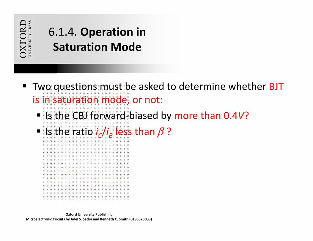
6.1.4. Operation in Saturation Mode
Two questions must be asked to determine whether BJT is in saturation mode, or not: Is the CBJ forward‐biased by more than 0.4V? Is the ratio iC/iB less than ?

Oxford University PublishingMicroelectronic Circuits by Adel S. Sedra and Kenneth C. Smith (0195323033)
6.1.5. The pnpTransistor
Figure 6.10: Current flow in a pnp transistor biased to operate in the active mode.

Oxford University PublishingMicroelectronic Circuits by Adel S. Sedra and Kenneth C. Smith (0195323033)
6.1.5. The pnpTransistor
Figure 6.11: Two large‐signal models for the pnp transistor operating in the active mode.
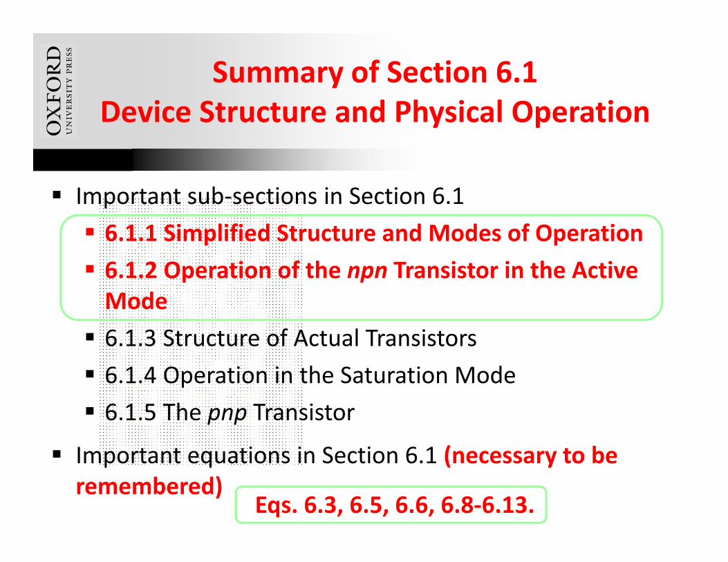
Summary of Section 6.1Device Structure and Physical Operation
Important sub‐sections in Section 6.1 6.1.1 Simplified Structure and Modes of Operation 6.1.2 Operation of the npn Transistor in the Active Mode 6.1.3 Structure of Actual Transistors 6.1.4 Operation in the Saturation Mode 6.1.5 The pnp Transistor
Important equations in Section 6.1 (necessary to be remembered)
Eqs. 6.3, 6.5, 6.6, 6.8‐6.13.
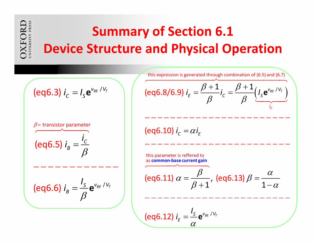
Summary of Section 6.1Device Structure and Physical Operation
intrinsic carrier density doping concentration of base
/
0
2
(eq6.3)
saturation current:
(eq6.4)
BE Tv VC S
E
n
n pS
E n iS
A
iNA
i I
A qD nI
W
A qD nI
W N
e
transistor parameter
/
(eq6.5)
(eq6.6) BE T
CB
v VSB
ii
Ii
e
this expression is generated through combination of (6.5) and (6.7)
/(eq6.8/6.9)
(eq6.10)
(eq6.11
1
)
1
BE T
C
v VE C S
C E
i
i i I
i i
e
this parameter is reffered
/
toas
(eq6.13)
(eq6.1
1 1
2)
,
BE Tv VSE
Ii
common‐base current gain
e