page 08 page 10 iii-v materials - boston electronics
TRANSCRIPT

2018, SEPTEMBER
PAGE 08COMPANYDEVELOPMENT PLANS
PAGE 16IMMERSION LENSESTECHNOLOGY– UNIQUE TECHNOLOGYFROM VIGO SYSTEM
PAGE 10
III-VMATERIALS
– FUTURE OFIR DETECTORS,
PROFESSORJÓZEF PIOTROWSKI

2 SEPTEMBER2018

4 THE CURRENT YEAR IS A KEY YEAR FOR OUR COMPANY
6 REBRANDING AND A NEW WEBSITE
8 COMPANY DEVELOPMENT PLANS
10 FUTURE OF IR DETECTORS III-V MATERIALS, PROFESSOR JÓZEF PIOTROWSKI
14 NEW InAsSb DETECTORS
16 IMMERSION LENSES TECHNOLOGY – UNIQUE TECHNOLOGY FROM VIGO SYSTEM
18 PIP – SMART PROGRAMMABLE DETECTION MODULE
20 AIP INTIR – ULTRA-FAST DETECTING MODULE WITH INTEGRATED COOLER CONTROLLER
22 INFRARED DETECTORS FOR SECURITY AND DEFENSE APPLICATIONS
24 R&D PROJECTS IMPLEMENTED AT VIGO SYSTEM
25 WATERSPY HIGH SENSITIVITY, PORTABLE PHOTONIC DEVICE FOR PERVASIVE WATER QUALITY ANALYSIS
28 AFTER HOURS
30 STRICTEST QUALITY STANDARDS
31 WHERE CAN YOU MEET US?
The recent years of the company operations have shown how popular our infrared detectors are on the global market.
3SEPTEMBER2018

This year has seen numerous changes in our company. Completed rebranding, pursuance of the VIGO 2020 strategy, expansion of the manufacturing plant including an increase in production capacity to 100 thousand detectors per year, introduction of a new material for developing detectors - these are one of the main changes you will be able to see in the near future.
THE CURRENT YEAR IS A KEY YEAR FOR OUR COMPANY
To make you familiar with all the topics related to the current changes in our company, I am presenting to you a VIGO System newsletter. I hope each of you will find some useful informa-tion on our technology and on the possibilities it offers, and also learn more about the work done at the company.
Without doubt, people are the most important element of our company’s operations. We would like to present to you the profiles of our employees in order to demon-strate that VIGO System is not only about innovative technology and work. We have been continuously devel-oping the best detectors in the world, taking care at the same time of the passions and interests of the people who create them.
Feel invited to read our newsletter!
Adam Piotrowski – President of the Management Board
4 SEPTEMBER2018

5SEPTEMBER 2018

REBRANDING AND A NEW WEBSITE
The aim of VIGO System S.A. operations is to continuously develop innovative infrared technologies. At the time of dynamic development of our company we want to take care also of the visual aspects. We make efforts to present to you information on our company and products in the most intuitive and user-friendly manner.
F or your convenience and in order to provide cle-arer and easier access to information, we have decided to create a new website, which you can find at www.vigo.com.pl. The website has a new
layout and includes the components you could see re-cently in the materials received from us.
The new website offers much more information on our company and on the applications of our infrared detec-tors. The main categories of application of our sensors are gas analysis and temperature control in fast moving objects. Those two solutions create a vast spectrum of possibilities to apply the products in various branches of industry, medicine, security, or environmental pro-tection. We want to show you in how many ways our products can be used, and how systems based on our detectors work.
An important component of the website is also a prod-uct configurator. It will allow you to find a specific type of detector and, if needed, to compare the parameters of products you are interested in. We hope the infor-mation on infrared detectors presented on the pages concerning our products will be even more clear for you and will meet your expectations.
Of course, we always encourage you to contact our specialists directly in order to discuss tailoring our products to your needs. To facilitate that form of con-tact, we have created a contact form through which an inquiry can be submitted to a competent person in the company. We intend to answer your questions within up to 24 hours from their reception. ■
The new website offers much more information on our company and on the applications of our infrared detectors.
6 SEPTEMBER2018

7SEPTEMBER 2018

The recent years of the company operations have shown how popular our infrared detectors are on the global market. In order to meet our customers’ needs, we are expanding our company, as a result of which the production capacity will be increased to 100 thousand detectors per year. The key components of the VIGO 2020 strategy pursuance are construction of a new manufacturing plant in Ożarów Mazowiecki and establishment of an application & implementation center.
COMPANY DEVELOPMENT PLANS
68 SEPTEMBER2018
The recent years of the company operations have shown how popular our infrared detectors are on the global market. In order to meet our customers’ needs, we are expanding our company, as a result of which the production capacity will be increased to 100 thousand detectors per year. The key components of the VIGO 2020 strategy pursuance are construction of a new manufacturing plant in Ożarów Mazowiecki and establishment of an application & implementation center.
COMPANY DEVELOPMENT PLANS
6
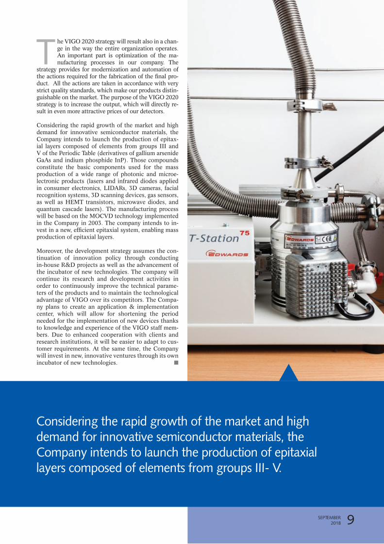
T he VIGO 2020 strategy will result also in a chan-ge in the way the entire organization operates. An important part is optimization of the ma-nufacturing processes in our company. The
strategy provides for modernization and automation of the actions required for the fabrication of the final pro-duct. All the actions are taken in accordance with very strict quality standards, which make our products distin-guishable on the market. The purpose of the VIGO 2020 strategy is to increase the output, which will directly re-sult in even more attractive prices of our detectors.
Considering the rapid growth of the market and high demand for innovative semiconductor materials, the Company intends to launch the production of epitax-ial layers composed of elements from groups III and V of the Periodic Table (derivatives of gallium arsenide GaAs and indium phosphide InP). Those compounds constitute the basic components used for the mass production of a wide range of photonic and microe-lectronic products (lasers and infrared diodes applied in consumer electronics, LIDARs, 3D cameras, facial recognition systems, 3D scanning devices, gas sensors, as well as HEMT transistors, microwave diodes, and quantum cascade lasers). The manufacturing process will be based on the MOCVD technology implemented in the Company in 2003. The company intends to in-vest in a new, efficient epitaxial system, enabling mass production of epitaxial layers.
Moreover, the development strategy assumes the con-tinuation of innovation policy through conducting in-house R&D projects as well as the advancement of the incubator of new technologies. The company will continue its research and development activities in order to continuously improve the technical parame-ters of the products and to maintain the technological advantage of VIGO over its competitors. The Compa-ny plans to create an application & implementation center, which will allow for shortening the period needed for the implementation of new devices thanks to knowledge and experience of the VIGO staff mem-bers. Due to enhanced cooperation with clients and research institutions, it will be easier to adapt to cus-tomer requirements. At the same time, the Company will invest in new, innovative ventures through its own incubator of new technologies. ■
Considering the rapid growth of the market and high demand for innovative semiconductor materials, the Company intends to launch the production of epitaxial layers composed of elements from groups III- V.
79SEPTEMBER 2018

FUTURE OF IR DETECTORS III–V MATERIALS, PROFESSOR JÓZEF PIOTROWSKI
10 SEPTEMBER2018

V igo specializes in medium-wave (2-8 µm) and long-wave (8-16 µm) IR detectors working in the ambient temperature or cooled thermo-electrically, referred to as MWIR HOT and
LWIR HOT detectors, respectively. IR HOT detectors are manufactured mainly from mercury cadmium tellu-ride (Hg1-xCdxTe), or more precisely from semiconduc-tor heterostructures made of that material. The said material enables manufacturing of detectors optimized for any wavelength, with the best parameters achieved so far. Unfortunately, both the material and the instru-ments made thereof have significant flaws - sensitivity to chemical, mechanical and thermal impact, high ma-nufacturing costs, and the necessity to use toxic heavy metals (Cd and Hg).
An alternative solution is using combinations of semicon-ductor A3B5 compounds containing metals (In, Al, Ga) and non-metals (As, Sb). The research on those materials has been conducted since 1960s, just as on Hg1-xCdxTe. Some binary A3B5 compounds (InAs and InSb) have been used for building near and mid infrared detectors. Unfortunately, the lattice constants of the A3B5 semicon-ductors vary significantly, which causes enormous prob-lems with the production of heterostructural devices that could be optimized for any spectral range.
The situation started to change at the end of the 20th century, when modern epitaxial technologies, particu-larly the MOCVD (Metal Organic Chemical Deposition) and MBE (Molecular Beam Epitaxy), were developed. The said technologies enabled manufacturing more complicated spatial structures comprising even of single layers of atoms. This offers a possibility to manufacture materials having unique properties, and to construct the most advanced heterostructural cascade detectors and detectors with enhanced absorption in a thin absorber.
I participated in works on those materials already dur-ing my one-year stay at the Center for Quantum De-vices at the Northwestern University in 1995. The re-sults were very promising, but Vigo had no possibility to purchase the expensive MOCVD and MBE systems.
The development of Vigo and its co-operation with the Military University of Technology enabled creation of a shared MBE laboratory specializing in the manu-facturing of A3B5 heterostructures with the use of an MBE system purchased from Riber.
Within less than 3 years the epitaxy technology was mastered for multiple classic semiconductor com-pounds (InAs, InSb, GaAs, GaSb, InAsSb, InAlSb, InGaAlAsSb) on GaAs substrate. In addition, hetero-structural medium- and long- wave photoelectric de-vices were manufactured whose parameters were simi-lar to those of devices based on Hg1-xCdxTe, and which at the same time were much more resistant to envi-ronmental impacts. In particular photodiodes based on InAsSb could not survive annealing at 160°C, whereas their Hg1-xCdxTe counterparts degraded at 100°C.
The last year also saw the mastering of the rudiments of manufacturing super lattice semiconductors which do not occur in the natural environment, super lattice heterostructures, and photoelectric devices based on them.
11SEPTEMBER2018
The situation started to change at the end of the 20th century, when modern epitaxial technologies, particularly the MOCVD (Metal Organic Chemical Vapour Deposi-tion) and MBE (Molecular Beam Epitaxy), were devel-oped. The said technologies enabled manufacturing more complicated spatial structures comprising even of single layers of atoms. This offers a possibility to manufacture materials having unique properties, and to construct the most advanced heterostructural cascade detectors and detectors with enhanced absorption in a thin absorber.

Super lattices are stacks of pairs of ultrathin layers of classic semiconductors, for example InAs/GaSb and InAs/InAsSb, and other. Those materials are potential-ly better than the Hg1-xCdxTe heterostructures. Unique solutions developed earlier as a part of production process of the Hg1-xCdxTe detectors, including improve-ment of the barrier layers technology, were also used in the construction of such devices.
One of the most important results was creation of a photoresistor with a long-wave limit of sensitiveness of ca. 11 µm, working in the ambient temperature or cooled thermoelectrically, whose parameters were bet-ter than those of the Hg1-xCdxTe detectors.
Further challenges include development of buffered GaAs substrates structurally, optically and electrically adjusted to the deposited heterostructures, decreasing the concentration of electrically active native impurities and of deep-level traps in the absorbers of detectors.
The potential possibilities of using detectors made of the A3B5 semiconductors are enormous. In the most optimistic scenario, they can totally supplant the Hg1-xCdxTe detectors for each spectral range and operating temperature. Yet, that will require exten-sive further research. The applications possible in the nearest future are:
■■ MWIR HOT photodiodes based on heterostructures with an InAsSb absorber. They can be used already now in applications requiring high reliability and resist-ance to weather impact, thus replacing the Hg1-xCdxTe photodiodes.
■■ The LWIR HOT based on InAsSb, and in particu-lar on InAs/InAsSb super lattices. The technology needs to be polished up, but the already achieved re-sults suggest a possibility to drive all the Hg1-xCdxTe counterparts from the market.
■■ It is assumed that in the further perspective of the years 2019-2020 advanced LWIR HOT photodiodes will be developed, made of InAs/InAsSb super lat-tice. Those will be cascade devices with enhanced radiation absorption, and with plasmonic nanoan-tennae in lieu of the retroreflector. That will enable manufacturing stable detectors with detectivity ap-proaching the fundamental limits, and characterized also by very high speed of response.
■■ Similar solutions could also be used in medium wave detectors.
FUTURE OF IR DETECTORS – INAS DETECTORS Vigo plans to purchase a modern MOCVD system ded-icated for A3B5 materials, which would enable a rad-ical increase in output and a decrease in the cost of manufacturing photoelectric devices. Research and development constitute very important components of the company’s activities. We believe that thanks to our discoveries and the technologies we have been devel-oping we will remain the leader of the global IR detec-tors market. ■
12 SEPTEMBER2018

One of the most important results was creation ofa photoresistor with a long-wave limit of sensitivenessof ca. 11 μm, working in the ambient temperatureor cooled thermoelectrically, whose parameterswere better than those of the Hg1-xCdxTe detectors.
13SEPTEMBER2018
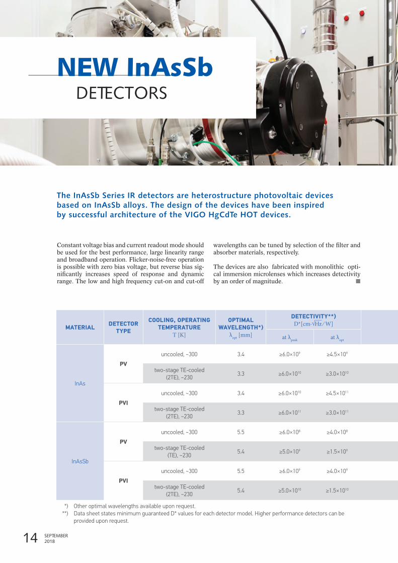
MATERIAL DETECTOR TYPE
COOLING, OPERATING TEMPERATURE
T [K]
OPTIMAL WAVELENGTH*)
λopt [mm]
DETECTIVITY**) D*[cm∙√Hz ∕ W]
CURRENT RESPONSIVITY
AT λopt Ri[
A/W]
TIME CONSTANT
τ [ns]
RESISTANCE OPTICAL AREA
PRODUCT R∙A [Ω∙cm2]
ACCEP-TANCE ANGLE
Φ[º], 1/2NA
OPTICAL AREA***)
[mm × mm]PACKAGE WINDOW****)
at λpeak at λopt
InAs
PV
uncooled, ~300 3.4 ≥6.0×10⁹ ≥4.5×10⁹ ≥1.1 ~20≥0.2
typ ~0.3≥90, 0.71 0.1×0.1 BNC, TO39 no window
two-stage TE-cooled (2TE), ~230
3.3 ≥6.0×10¹⁰ ≥3.0×10¹⁰ ≥1.2 ~15≥20
typ ~40TO8, TO66 wedged Al2O3
PVI
uncooled, ~300 3.4 ≥6.0×10¹⁰ ≥4.5×10¹¹ ≥1.1 ~20≥20
typ ~30~35, 1.62 1×1 BNC, TO39 no window
two-stage TE-cooled (2TE), ~230
3.3 ≥6.0×10¹¹ ≥3.0×10¹¹ ≥1.2 ~15≥2000
typ ~4000TO8, TO66 wedged Al2O3
InAsSb
PV
uncooled, ~300 5.5 ≥6.0×10⁸ ≥4.0×10⁸ ≥1.3 +)≥0.003
typ ~0.005≥90, 0.71 0.1×0.1 BNC, TO39 no window
two-stage TE-cooled (TE), ~230
5.4 ≥5.0×10⁹ ≥1.5×10⁹ ≥1.5 +)≥0.15
typ ~0.2TO8, TO66 wedged Al2O3
PVI
uncooled, ~300 5.5 ≥6.0×10⁹ ≥4.0×10⁹ ≥1.3 +)≥0.3
typ ~0.5~35, 1.62 1×1 BNC, TO39 no window
two-stage TE-cooled (2TE), ~230
5.4 ≥5.0×10¹⁰ ≥1.5×10¹⁰ ≥1.5 +)≥15
typ ~20TO8, TO66 wedged Al2O3
The InAsSb Series IR detectors are heterostructure photovoltaic devices based on InAsSb alloys. The design of the devices have been inspired by successful architecture of the VIGO HgCdTe HOT devices.
Constant voltage bias and current readout mode should be used for the best performance, large linearity range and broadband operation. Flicker-noise-free operation is possible with zero bias voltage, but reverse bias sig-nificantly increases speed of response and dynamic range. The low and high frequency cut-on and cut-off
wavelengths can be tuned by selection of the filter and absorber materials, respectively.
The devices are also fabricated with monolithic opti-cal immersion microlenses which increases detectivity by an order of magnitude. ■
*) Other optimal wavelengths available upon request. **) Data sheet states minimum guaranteed D* values for each detector model. Higher performance detectors can be
provided upon request.
NEW InAsSb DETECTORS
10
MATERIAL DETECTOR TYPE
COOLING, OPERATING TEMPERATURE
T [K]
OPTIMAL WAVELENGTH*)
λopt [mm]
DETECTIVITY**) D*[cm∙√Hz ∕ W]
CURRENT RESPONSIVITY
AT λopt Ri[
A/W]
TIME CONSTANT
τ [ns]
RESISTANCE OPTICAL AREA
PRODUCT R∙A [Ω∙cm2]
ACCEP-TANCE ANGLE
Φ[º], 1/2NA
OPTICAL AREA***)
[mm × mm]PACKAGE WINDOW****)
at λpeak at λopt
InAs
PV
uncooled, ~300 3.4 ≥6.0×10⁹ ≥4.5×10⁹ ≥1.1 ~20≥0.2
typ ~0.3≥90, 0.71 0.1×0.1 BNC, TO39 no window
two-stage TE-cooled (2TE), ~230
3.3 ≥6.0×10¹⁰ ≥3.0×10¹⁰ ≥1.2 ~15≥20
typ ~40TO8, TO66 wedged Al2O3
PVI
uncooled, ~300 3.4 ≥6.0×10¹⁰ ≥4.5×10¹¹ ≥1.1 ~20≥20
typ ~30~35, 1.62 1×1 BNC, TO39 no window
two-stage TE-cooled (2TE), ~230
3.3 ≥6.0×10¹¹ ≥3.0×10¹¹ ≥1.2 ~15≥2000
typ ~4000TO8, TO66 wedged Al2O3
InAsSb
PV
uncooled, ~300 5.5 ≥6.0×10⁸ ≥4.0×10⁸ ≥1.3 +)≥0.003
typ ~0.005≥90, 0.71 0.1×0.1 BNC, TO39 no window
two-stage TE-cooled (TE), ~230
5.4 ≥5.0×10⁹ ≥1.5×10⁹ ≥1.5 +)≥0.15
typ ~0.2TO8, TO66 wedged Al2O3
PVI
uncooled, ~300 5.5 ≥6.0×10⁹ ≥4.0×10⁹ ≥1.3 +)≥0.3
typ ~0.5~35, 1.62 1×1 BNC, TO39 no window
two-stage TE-cooled (2TE), ~230
5.4 ≥5.0×10¹⁰ ≥1.5×10¹⁰ ≥1.5 +)≥15
typ ~20TO8, TO66 wedged Al2O3
*) Other optimal wavelengths available upon request. **) Data sheet states minimum guaranteed D* values for each detector model. Higher performance detectors can be
provided upon request.
***) Other optical areas available upon request. ****) Other windows available upon request. +) parameter dependent on device construction, more details upon request
3MARZEC 20182 WRZESIEŃ
201814 SEPTEMBER2018

MATERIAL DETECTOR TYPE
COOLING, OPERATING TEMPERATURE
T [K]
OPTIMAL WAVELENGTH*)
λopt [mm]
DETECTIVITY**) D*[cm∙√Hz ∕ W]
CURRENT RESPONSIVITY
AT λopt Ri[
A/W]
TIME CONSTANT
τ [ns]
RESISTANCE OPTICAL AREA
PRODUCT R∙A [Ω∙cm2]
ACCEP-TANCE ANGLE
Φ[º], 1/2NA
OPTICAL AREA***)
[mm × mm]PACKAGE WINDOW****)
at λpeak at λopt
InAs
PV
uncooled, ~300 3.4 ≥6.0×10⁹ ≥4.5×10⁹ ≥1.1 ~20≥0.2
typ ~0.3≥90, 0.71 0.1×0.1 BNC, TO39 no window
two-stage TE-cooled (2TE), ~230
3.3 ≥6.0×10¹⁰ ≥3.0×10¹⁰ ≥1.2 ~15≥20
typ ~40TO8, TO66 wedged Al2O3
PVI
uncooled, ~300 3.4 ≥6.0×10¹⁰ ≥4.5×10¹¹ ≥1.1 ~20≥20
typ ~30~35, 1.62 1×1 BNC, TO39 no window
two-stage TE-cooled (2TE), ~230
3.3 ≥6.0×10¹¹ ≥3.0×10¹¹ ≥1.2 ~15≥2000
typ ~4000TO8, TO66 wedged Al2O3
InAsSb
PV
uncooled, ~300 5.5 ≥6.0×10⁸ ≥4.0×10⁸ ≥1.3 +)≥0.003
typ ~0.005≥90, 0.71 0.1×0.1 BNC, TO39 no window
two-stage TE-cooled (TE), ~230
5.4 ≥5.0×10⁹ ≥1.5×10⁹ ≥1.5 +)≥0.15
typ ~0.2TO8, TO66 wedged Al2O3
PVI
uncooled, ~300 5.5 ≥6.0×10⁹ ≥4.0×10⁹ ≥1.3 +)≥0.3
typ ~0.5~35, 1.62 1×1 BNC, TO39 no window
two-stage TE-cooled (2TE), ~230
5.4 ≥5.0×10¹⁰ ≥1.5×10¹⁰ ≥1.5 +)≥15
typ ~20TO8, TO66 wedged Al2O3
The InAsSb Series IR detectors are heterostructure photovoltaic devices based on InAsSb alloys. The design of the devices have been inspired by successful architecture of the VIGO HgCdTe HOT devices.
Constant voltage bias and current readout mode should be used for the best performance, large linearity range and broadband operation. Flicker-noise-free operation is possible with zero bias voltage, but reverse bias sig-nificantly increases speed of response and dynamic range. The low and high frequency cut-on and cut-off
wavelengths can be tuned by selection of the filter and absorber materials, respectively.
The devices are also fabricated with monolithic opti-cal immersion microlenses which increases detectivity by an order of magnitude. ■
*) Other optimal wavelengths available upon request. **) Data sheet states minimum guaranteed D* values for each detector model. Higher performance detectors can be
provided upon request.
NEW InAsSb DETECTORS
10
MATERIAL DETECTOR TYPE
COOLING, OPERATING TEMPERATURE
T [K]
OPTIMAL WAVELENGTH*)
λopt [mm]
DETECTIVITY**) D*[cm∙√Hz ∕ W]
CURRENT RESPONSIVITY
AT λopt Ri[
A/W]
TIME CONSTANT
τ [ns]
RESISTANCE OPTICAL AREA
PRODUCT R∙A [Ω∙cm2]
ACCEP-TANCE ANGLE
Φ[º], 1/2NA
OPTICAL AREA***)
[mm × mm]PACKAGE WINDOW****)
at λpeak at λopt
InAs
PV
uncooled, ~300 3.4 ≥6.0×10⁹ ≥4.5×10⁹ ≥1.1 ~20≥0.2
typ ~0.3≥90, 0.71 0.1×0.1 BNC, TO39 no window
two-stage TE-cooled (2TE), ~230
3.3 ≥6.0×10¹⁰ ≥3.0×10¹⁰ ≥1.2 ~15≥20
typ ~40TO8, TO66 wedged Al2O3
PVI
uncooled, ~300 3.4 ≥6.0×10¹⁰ ≥4.5×10¹¹ ≥1.1 ~20≥20
typ ~30~35, 1.62 1×1 BNC, TO39 no window
two-stage TE-cooled (2TE), ~230
3.3 ≥6.0×10¹¹ ≥3.0×10¹¹ ≥1.2 ~15≥2000
typ ~4000TO8, TO66 wedged Al2O3
InAsSb
PV
uncooled, ~300 5.5 ≥6.0×10⁸ ≥4.0×10⁸ ≥1.3 +)≥0.003
typ ~0.005≥90, 0.71 0.1×0.1 BNC, TO39 no window
two-stage TE-cooled (TE), ~230
5.4 ≥5.0×10⁹ ≥1.5×10⁹ ≥1.5 +)≥0.15
typ ~0.2TO8, TO66 wedged Al2O3
PVI
uncooled, ~300 5.5 ≥6.0×10⁹ ≥4.0×10⁹ ≥1.3 +)≥0.3
typ ~0.5~35, 1.62 1×1 BNC, TO39 no window
two-stage TE-cooled (2TE), ~230
5.4 ≥5.0×10¹⁰ ≥1.5×10¹⁰ ≥1.5 +)≥15
typ ~20TO8, TO66 wedged Al2O3
FEATURES
■■ Ambient temperature or Peltier cooling■■ No flicker noise for zero bias voltage■■ Operation from DC to high frequencies■■ Perfect match to fast electronics■■ Wide dynamic range■■ Improved reliability compared to HgCdTe devices■■ Low cost■■ Custom design upon request
SPECTRAL CHARACTERISTICS:
3 3,5 4 4,5 5 5,52 2,5 3 3,5 λ, μmλ, μm1E8
1E9
1E10
1E11
1E9
1E10
1E11
1E12
D*,
cm
Hz-½
W-1 InAsSbInAs
PV-5.5
PV-2TE-5.5
PVI-5.5
PVI-2TE-5.5
PVI-3.4
PVI-2TE-3.3
PV-3.4
PV-2TE-3.3
***) Other optical areas available upon request. ****) Other windows available upon request. +) parameter dependent on device construction, more details upon request
11SEPTEMBER 2018
MATERIAL DETECTOR TYPE
COOLING, OPERATING TEMPERATURE
T [K]
OPTIMAL WAVELENGTH*)
λopt [mm]
DETECTIVITY**) D*[cm∙√Hz ∕ W]
CURRENT RESPONSIVITY
AT λopt Ri[
A/W]
TIME CONSTANT
τ [ns]
RESISTANCE OPTICAL AREA
PRODUCT R∙A [Ω∙cm2]
ACCEP-TANCE ANGLE
Φ[º], 1/2NA
OPTICAL AREA***)
[mm × mm]PACKAGE WINDOW****)
at λpeak at λopt
InAs
PV
uncooled, ~300 3.4 ≥6.0×10⁹ ≥4.5×10⁹ ≥1.1 ~20≥0.2
typ ~0.3≥90, 0.71 0.1×0.1 BNC, TO39 no window
two-stage TE-cooled (2TE), ~230
3.3 ≥6.0×10¹⁰ ≥3.0×10¹⁰ ≥1.2 ~15≥20
typ ~40TO8, TO66 wedged Al2O3
PVI
uncooled, ~300 3.4 ≥6.0×10¹⁰ ≥4.5×10¹¹ ≥1.1 ~20≥20
typ ~30~35, 1.62 1×1 BNC, TO39 no window
two-stage TE-cooled (2TE), ~230
3.3 ≥6.0×10¹¹ ≥3.0×10¹¹ ≥1.2 ~15≥2000
typ ~4000TO8, TO66 wedged Al2O3
InAsSb
PV
uncooled, ~300 5.5 ≥6.0×10⁸ ≥4.0×10⁸ ≥1.3 +)≥0.003
typ ~0.005≥90, 0.71 0.1×0.1 BNC, TO39 no window
two-stage TE-cooled (TE), ~230
5.4 ≥5.0×10⁹ ≥1.5×10⁹ ≥1.5 +)≥0.15
typ ~0.2TO8, TO66 wedged Al2O3
PVI
uncooled, ~300 5.5 ≥6.0×10⁹ ≥4.0×10⁹ ≥1.3 +)≥0.3
typ ~0.5~35, 1.62 1×1 BNC, TO39 no window
two-stage TE-cooled (2TE), ~230
5.4 ≥5.0×10¹⁰ ≥1.5×10¹⁰ ≥1.5 +)≥15
typ ~20TO8, TO66 wedged Al2O3
*) Other optimal wavelengths available upon request. **) Data sheet states minimum guaranteed D* values for each detector model. Higher performance detectors can be
provided upon request.
***) Other optical areas available upon request. ****) Other windows available upon request. +) parameter dependent on device construction, more details upon request
3MARZEC 20182 WRZESIEŃ
2018 15SEPTEMBER 2018

WHAT IS OPTICAL IMMERSION?Optical immersion means the use of a certain type of lens, which is an integral part of an IR detector. The lens enables collecting an amount of optical radiation falling on the de-vice larger than the one that could be collect-ed only due to the physical area of the device. As a result, the detector picks up more usable signal - as much as a larger device - while re-taining a smaller area.
IMMERSION LENSES TECHNOLOGY – UNIQUE TECHNOLOGY FROM VIGO SYSTEM
There are many ways of improving detector parameters with the use of optical devices (including, amongst others, optical cones, concentrators), but only the optical immersion used by VIGO System enables improving the detectivity of a detector in the simplest way possible - without losses, without aligning, and at a very small expense.
WHAT IS THE ADVANTAGE OF USING A SMALLER DETECTOR? The answer is a noise reduction. A smaller de-tector area means a considerable decrease in the level of noise level generated by the device.
WHAT ARE THE UNIQUE FEATURES OF THE VIGO SYSTEM LENSES?At VIGO System, the optical immersion is created directly with the use of the substrate on which the active layer of the detector is placed. This means the lens is an integral part of the device - no adhesives or other joints that could generate losses are used for its fabrication. A monolithic lens does not need to be aligned by the customer in any way, and it reaches its maximum efficiency already during the manufacturing process. This is a unique technology developed and used in IR detectors solely by the VIGO Sys-tem company.
TO WHAT EXTENT CAN PARAMETERS OF A DEVICE BE IMPROVED WITH OPTICAL IMMERSION?The degree of detector parameters improve-ment depends on the material from which the immersion lens is made. Generally speaking, the detectivity of a device is im-proved:- n times if a hemispherical lens is used - n2 times if a hyperhemispherical lens is used where n is the refractive index of the lens. In the VIGO System detectors com-prising a GaAs substrate and an integrated immersion lens made of the same material, the refractive index of the lens is equal to 3.3. That means the detectivity is improved 3.3 times in a detector with a hemispherical lens, and nearly 11 times in a detector with a hy-perhemispherical lens. Both types of lenses (hemispherical and hyperhemispherical) are available from the VIGO System products catalogue. A hyperhemispherical lens is of-
2
4
1
3
1216 SEPTEMBER2018
2

WHAT IS OPTICAL IMMERSION?Optical immersion means the use of a certain type of lens, which is an integral part of an IR detector. The lens enables collecting an amount of optical radiation falling on the de-vice larger than the one that could be collect-ed only due to the physical area of the device. As a result, the detector picks up more usable signal - as much as a larger device - while re-taining a smaller area.
IMMERSION LENSES TECHNOLOGY – UNIQUE TECHNOLOGY FROM VIGO SYSTEM
There are many ways of improving detector parameters with the use of optical devices (including, amongst others, optical cones, concentrators), but only the optical immersion used by VIGO System enables improving the detectivity of a detector in the simplest way possible - without losses, without aligning, and at a very small expense.
WHAT IS THE ADVANTAGE OF USING A SMALLER DETECTOR? The answer is a noise reduction. A smaller de-tector area means a considerable decrease in the level of noise level generated by the device.
WHAT ARE THE UNIQUE FEATURES OF THE VIGO SYSTEM LENSES?At VIGO System, the optical immersion is created directly with the use of the substrate on which the active layer of the detector is placed. This means the lens is an integral part of the device - no adhesives or other joints that could generate losses are used for its fabrication. A monolithic lens does not need to be aligned by the customer in any way, and it reaches its maximum efficiency already during the manufacturing process. This is a unique technology developed and used in IR detectors solely by the VIGO Sys-tem company.
TO WHAT EXTENT CAN PARAMETERS OF A DEVICE BE IMPROVED WITH OPTICAL IMMERSION?The degree of detector parameters improve-ment depends on the material from which the immersion lens is made. Generally speaking, the detectivity of a device is im-proved:- n times if a hemispherical lens is used - n2 times if a hyperhemispherical lens is used where n is the refractive index of the lens. In the VIGO System detectors com-prising a GaAs substrate and an integrated immersion lens made of the same material, the refractive index of the lens is equal to 3.3. That means the detectivity is improved 3.3 times in a detector with a hemispherical lens, and nearly 11 times in a detector with a hy-perhemispherical lens. Both types of lenses (hemispherical and hyperhemispherical) are available from the VIGO System products catalogue. A hyperhemispherical lens is of-
2
4
1
3
12
SUMMARY■■ immersion lenses are optical elements that improve the detectivity of an infrared detector
■■ the lenses used at VIGO System generate no losses, require no align-ment, and offer maximum efficiency immediately after they are man-ufactured
■■ the immersion may limit the angle of view of a detector (this applies to hyperhemispherical immersion lenses)
■■ detectors with immersion lenses are perfect for applications where the power of the radiation source is low, and for applications where the detector’s detectivity is the most important parameter.
fered as a standard. It needs to be stressed that if a hyperhemispherical lens is used, the angle of view (acceptance angle) of the detector is limited to 35 degrees, which may be a significant limitation as far as certain applications are concerned. The acceptance angle of a detector with a hemispherical lens remains unchanged and is 180 degrees.
FOR WHAT APPLICATIONS IS THE OPTICAL IMMERSION RECOMMENDED?A detector with an immersion lens is best suited for operation with low power of op-tical signal, which means the applications where the highest detectivity of the detec-tor is required. The use of optical immer-sion enables improving the signal-to-noise ratio almost 11 times without any need for additional customer’s interference with the measurement system. It needs to be stressed that although the use of optical immersion gives extraordinary results in applications with low signal levels, if strong sources of radiation are used, an immersion detector does not need to be necessarily chosen. Why? If the optical signal is strong enough, the high power of radiation enables equalizing the signal-to-noise ratio in a flat detector without a lens, just as if the immer-sion technology was used.
Detailed information on immersion detec-tors, as well as assistance in selecting a de-tector for your applications is available from local distributors or from the sales force of the VIGO System company. ■
5
FLAT DETECTORDetectivity D*
DETECTOR WITH HEMISPHERE IMMERSION LENSDetectivity 3.3D*
DETECTOR WITH HYPER HEMISPHERE IMMERSION LENS
Detectivity 10.9D*
DETECTOR L10.9
DETECTOR L3.3
DETECTOR
L
13
Jacek Kułakowski
17SEPTEMBER 2018

PIP – SMART PROGRAMMABLE DETECTION MODULE
An IR detection module combining excellent electric parameters, such ashigh signal-to-noise ratio, wide pass band (exceeding 250 MHz), and minimum linear and non-linear distortion with flexibility, reliability and high resistance to surges and interference.
The module is fully configurable with the use of software, which makes it perfectly suitable for application both in industrial conditions, whe-re repeatability and reliability count, and in la-
boratory conditions, where flexibility, convenience of operation, and the best possible electric parameters are of paramount importance.
In addition, the device is equipped with an analog-to-dig-ital converter enabling the monitoring of power supply, voltage on the detector, voltage after the first and last amplification stages, as well as potentials on the ther-mistor and on the thermoelectric cooler of the detector. The aforementioned solutions together with the protec-tions implemented in the device secure it against abnor-mal operating conditions, and in the case of a failure the device can be diagnosed remotely without the use of any additional measuring instruments.
Thanks to an option enabling change of parameters on the fly, and to a possibility to save 4 different device
configurations and to restore them on demand, high detectivity and DC operation, as well as high speed of device operation and low noise amplification within the high frequency range can be obtained, even though the system is equipped with a single detector.
The activation time of the device consisting of an am-plifier and a detector is minimized, as all the parame-ters are configured with the use of software.
The aforementioned advantages of the device do not cause any lowering of its electric parameters.
The external dimensions are identical with those of the module without the digital part incorporated.
In combination with the SmartTec controller, particularly with its Advanced version (with an LCD), the device of-fers an unmatched convenience of operation and can be used in an even larger number of applications. ■
14
as high signal-to-noise ratio, wide pass band (exceeding 250 MHz),
18 SEPTEMBER2018

PIP – SMART PROGRAMMABLE DETECTION MODULE
An IR detection module combining excellent electric parameters, such ashigh signal-to-noise ratio, wide pass band (exceeding 250 MHz), and minimum linear and non-linear distortion with flexibility, reliability and high resistance to surges and interference.
The module is fully configurable with the use of software, which makes it perfectly suitable for application both in industrial conditions, whe-re repeatability and reliability count, and in la-
boratory conditions, where flexibility, convenience of operation, and the best possible electric parameters are of paramount importance.
In addition, the device is equipped with an analog-to-dig-ital converter enabling the monitoring of power supply, voltage on the detector, voltage after the first and last amplification stages, as well as potentials on the ther-mistor and on the thermoelectric cooler of the detector. The aforementioned solutions together with the protec-tions implemented in the device secure it against abnor-mal operating conditions, and in the case of a failure the device can be diagnosed remotely without the use of any additional measuring instruments.
Thanks to an option enabling change of parameters on the fly, and to a possibility to save 4 different device
configurations and to restore them on demand, high detectivity and DC operation, as well as high speed of device operation and low noise amplification within the high frequency range can be obtained, even though the system is equipped with a single detector.
The activation time of the device consisting of an am-plifier and a detector is minimized, as all the parame-ters are configured with the use of software.
The aforementioned advantages of the device do not cause any lowering of its electric parameters.
The external dimensions are identical with those of the module without the digital part incorporated.
In combination with the SmartTec controller, particularly with its Advanced version (with an LCD), the device of-fers an unmatched convenience of operation and can be used in an even larger number of applications. ■
14
PREAMPLIFIER SPECIFICATION
PARAMETER SYMBOL UNIT TYPICAL VALUE CONDITIONS, REMARKS
Input Noise Voltage Density en
nV √Hz 0.95 fo = 10 kHz2)
Input Noise Current Density in
pA √Hz
4.51) 7.01)
first stage transimpedance = 5 kΩ first stage transimpedance = 1 kΩ
Low Cut-Off Frequency flo Hz DC/1k user configurable by software
High Cut-Off Frequency fhi Hz 150k/1.5M/20M3)
1.5M/15M/200M3)
maximum values, with limited range of detector with „in circuit” filter activated
Transimpedance KiVA
250 – 25k 1.25k – 125k
first stage transimpedace = 5 kΩ first stage transimpedace = 1 kΩ
Output Impedance Rout Ω 50
Output Voltage Swing Vout V ±1 with 50 Ω load applied
Output Voltage Offset Voff mV max ±254) max ±10
DC coupling set AC coupling set
Power Supply Voltage Vsup V ±9
Power Supply Current Isup mA typ ±80 max ±100
Dimensions -mm × mm
× mm
40×81.3×40 40×82.8×40 40×84.3×40
width×depth×height - with 2TE width×depth×height - with 3TE width×depth×height - with 4TE
Operation Tempearture T °C +5...+35
Storage Temperature - °C -10...+50
Relative Humidity - % 10...90
Electrical characteristics @Ta = 20°C. 1) The preamplifier noise may significantly reduce the system performance in some situations. This happens for large capaci-
tance detectors operating at high frequencies. 2) f0 – noise measurement frequency. 3) Depending on preamplifier option. 4) Measured with equivalent resistor at the input instead of the detector. It’s to avoid the environmental thermal radiation’s impact.
15SEPTEMBER 2018
f0 = 10 kHz2)
19SEPTEMBER 2018
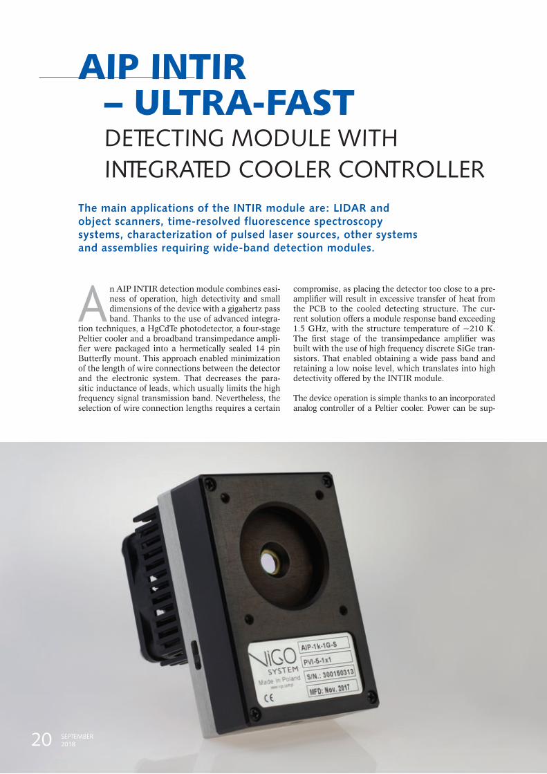
AIP INTIR – ULTRA-FAST DETECTING MODULE WITH INTEGRATED COOLER CONTROLLER
A n AIP INTIR detection module combines easi-ness of operation, high detectivity and small dimensions of the device with a gigahertz pass band. Thanks to the use of advanced integra-
tion techniques, a HgCdTe photodetector, a four-stage Peltier cooler and a broadband transimpedance ampli-fier were packaged into a hermetically sealed 14 pin Butterfly mount. This approach enabled minimization of the length of wire connections between the detector and the electronic system. That decreases the para-sitic inductance of leads, which usually limits the high frequency signal transmission band. Nevertheless, the selection of wire connection lengths requires a certain
compromise, as placing the detector too close to a pre-amplifier will result in excessive transfer of heat from the PCB to the cooled detecting structure. The cur-rent solution offers a module response band exceeding 1.5 GHz, with the structure temperature of ~210 K. The first stage of the transimpedance amplifier was built with the use of high frequency discrete SiGe tran-sistors. That enabled obtaining a wide pass band and retaining a low noise level, which translates into high detectivity offered by the INTIR module.
The device operation is simple thanks to an incorporated analog controller of a Peltier cooler. Power can be sup-
The main applications of the INTIR module are: LIDAR and object scanners, time-resolved fluorescence spectroscopy systems, characterization of pulsed laser sources, other systems and assemblies requiring wide-band detection modules.
1620 SEPTEMBER2018

AIP INTIR – ULTRA-FAST DETECTING MODULE WITH INTEGRATED COOLER CONTROLLER
A n AIP INTIR detection module combines easi-ness of operation, high detectivity and small dimensions of the device with a gigahertz pass band. Thanks to the use of advanced integra-
tion techniques, a HgCdTe photodetector, a four-stage Peltier cooler and a broadband transimpedance ampli-fier were packaged into a hermetically sealed 14 pin Butterfly mount. This approach enabled minimization of the length of wire connections between the detector and the electronic system. That decreases the para-sitic inductance of leads, which usually limits the high frequency signal transmission band. Nevertheless, the selection of wire connection lengths requires a certain
compromise, as placing the detector too close to a pre-amplifier will result in excessive transfer of heat from the PCB to the cooled detecting structure. The cur-rent solution offers a module response band exceeding 1.5 GHz, with the structure temperature of ~210 K. The first stage of the transimpedance amplifier was built with the use of high frequency discrete SiGe tran-sistors. That enabled obtaining a wide pass band and retaining a low noise level, which translates into high detectivity offered by the INTIR module.
The device operation is simple thanks to an incorporated analog controller of a Peltier cooler. Power can be sup-
The main applications of the INTIR module are: LIDAR and object scanners, time-resolved fluorescence spectroscopy systems, characterization of pulsed laser sources, other systems and assemblies requiring wide-band detection modules.
16
ELECTRICAL PARAMETERS
Transimpedance TIA = 1,2 kΩ
Rise time tr 10%-90% = 202 ps
Fall timetf 10%-90% = 174 ps
(12% undershoot)
-3 dB analog bandwidth
f-3dB = 202 ps
Full width at half maximum
FWHM = 320 ps
OPTICAL PARAMETERS
Detectivity D* = 2,5∙109 [cm∙√Hz ∕ W]
Voltage responsivity Rv = 1,6 kV ∕ W
plied to the entire device with a standard plug-in power supply unit. Thanks to its small dimensions (73 mm x 50 mm x 55 mm), the module can be easily incorporated in industrial and laboratory measuring systems.
The devices is equipped with two analog outputs:
■■ AC - main broadband signal output - AC coupling with a possibility to modify amplification and the lower cut-off frequency.
■■ DC - DC signal output, for example for controlling the average optical power received by the detector. ■
MODULE INTEGRATED WITH PVI, DETECTORM
odul
e re
spon
se [V
]
-0.02
0
-1 -0.5 0 0.5 1 1.5 2 2.5 3 3.5 4
0.02
0.04
0.06
0.08
0.1
0.12
0.14
Time [ns]
10 µm Pulsed QCL
PULSE RESPONSE OF THE HIGH SPEED MODULE
An AIP INTIR detection module combines easiness of operation, high detectivity and small dimensions of the device with a gigahertz pass band.
17
Mateusz Żbik
21SEPTEMBER2018

INFRARED DETECTORS FOR SECURITY AND DEFENSE APPLICATIONS
SMART MUNITIONSTanks and other military vehicles emit particularly large amounts of heat (mid infrared radiation) as a re-sult of engine and equipment operation.
That enables detecting such objects and distinguishing them from the surroundings with the use of infrared detectors. Thanks to high limits of detection, VIGO System detectors may be used for precise and efficient homing on moving vehicles directly before the attack.
The use of a smart munitions system requires only minimum participation from the user. First, a carrier missile is fired, which delivers explosive material to the target area. Next, the main charge with a homing system is separated from the missile and falls freely towards the earth. After the IR sensors are activated
and a ground target is detected, the object is identified by means of comparing its parameters with patterns stored in a database. Finally, the proper attack is per-formed and the target is effectively neutralized.
DIRCM & CIRCMHighly sensitive infrared detectors manufactured by VIGO System enable deceiving such systems.
That is achieved by means of cooperation between detectors and active countermeasure systems equipped with their own laser sources that disturb the operation of missiles.
A laser installed on the protected object remains off till a threat is detected, so as not to reveal the location of the object. It is the job of an accurate infrared detector from
Vigo system s.a. Has developed a unique technology for manufacturing instruments for quick and convenient detection of 1 – 16 μm infrared radiation. The instruments operate in ambient temperature or are cooled with simple and inexpensive thermoelectric coolers.
18
Vigo System S.A. has developed a unique technology for manufacturing instruments for quick and convenient detection of 1 – 16 μm infrared radiation. The instruments operate in ambient temperature or are cooled with simple and inexpensive thermoelectric coolers.
22 SEPTEMBER2018

Infrared guided missiles are an example of the newest generation of weapons, which thanks to their resilience to common and widely used thermal countermeasures pose a real threat to aircraft and helicopters.
INFRARED DETECTORS FOR SECURITY AND DEFENSE APPLICATIONS
SMART MUNITIONSTanks and other military vehicles emit particularly large amounts of heat (mid infrared radiation) as a re-sult of engine and equipment operation.
That enables detecting such objects and distinguishing them from the surroundings with the use of infrared detectors. Thanks to high limits of detection, VIGO System detectors may be used for precise and efficient homing on moving vehicles directly before the attack.
The use of a smart munitions system requires only minimum participation from the user. First, a carrier missile is fired, which delivers explosive material to the target area. Next, the main charge with a homing system is separated from the missile and falls freely towards the earth. After the IR sensors are activated
and a ground target is detected, the object is identified by means of comparing its parameters with patterns stored in a database. Finally, the proper attack is per-formed and the target is effectively neutralized.
DIRCM & CIRCMHighly sensitive infrared detectors manufactured by VIGO System enable deceiving such systems.
That is achieved by means of cooperation between detectors and active countermeasure systems equipped with their own laser sources that disturb the operation of missiles.
A laser installed on the protected object remains off till a threat is detected, so as not to reveal the location of the object. It is the job of an accurate infrared detector from
Vigo system s.a. Has developed a unique technology for manufacturing instruments for quick and convenient detection of 1 – 16 μm infrared radiation. The instruments operate in ambient temperature or are cooled with simple and inexpensive thermoelectric coolers.
18
Infrared guided missiles are an example of the newest generation of weapons, which thanks to their resilience to common and widely used thermal countermeasures pose a real threat to aircraft and helicopters.
VIGO System to detect a threat. Such a detector records infrared radiation emitted by the missile, and immediate-ly passes the information on threat to the missile counter-measure system and to the aircraft/helicopter crew. Next, an active countermeasure system aims its own laser beam on the missile, so that it interprets the beam as the ra-diation incoming from the target. By means of suitable modulation of the laser signal, the missile is diverted from the target and neutralized in a safe area.
STAND - OFF DETECTIONTherefore, there are plans to create on the basis of infrared detectors remotely controlled, long-range systems for searching places where explosions, gas at-tacks or terrorist attacks occurred, and for subsequent transmission of information on the hazards and threats present in a given location.
The present stand-off detection systems are large in-stallations with complicated optical systems and intri-cate spectroscopes and analyzers. Thanks to the ongo-ing progress in miniaturization, they may soon become compact systems, easy to transport and convenient to use. Because of their small dimensions and no need for cooling with liquid nitrogen, infrared detectors from VIGO System can be used directly for construction of handy systems for detecting poisonous or flammable gases. Such systems are characterized by easy opera-tion and small power consumption enabling their use in difficult conditions.
PROTECTION OF AN AREA AGAINST ACTS OF TERRORISMIn the process of manufacturing illegal products, dis-tinctive and unique substances are produced, which can be detected by means analyzing The infrared spec-trum of vapor or examining liquid or solid wastes. The VIGO System infrared detectors provide a possibili-ty to scan air over large areas with the use of drones or aircraft, and to monitor sewage systems and solid wastes with the use of other measuring devices. The projects implemented so far with the use of VIGO Sys-tem detectors were focused on building a system for detecting from large distances (100-400 m) explosives or their substrates in the liquid phase and in the air. The development and use of such devices would mean a significant progress in operations conducted in coun-tries engulfed by conflicts, or in territories controlled by terrorist organizations. ■
1923SEPTEMBER2018

THESE ARE THE HORIZON 2020 PROJECTSIN WHICH SPECIALISTS FROM VIGO SYSTEM ARE INVOLVED
A s members of international project consortia, we have been continuously involved in imple-mentation of numerous research projects both home and abroad. VIGO System S.A. partici-
pates in five projects implemented under a European program named Horizon 2020. It is the biggest rese-arch and innovation program in the history of the Eu-ropean Union. Its total budget available for seven years amounts to nearly €80 billion, of which €2.8 billion will be earmarked for scientific research and innovation.
In the consecutive issues of our quarterly newsletter we would like to present to you information on each of the pro-jects in which we are involved. Now we invite you to find out more on the WaterSpy project, which, after its completion, will have a real impact on our health and safety. ■
A factor of great importance for company development is connecting the worlds of business and science. VIGO System has been putting much stress on research and development of new technologies.
R&D PROJECTS
IMPLEMENTED AT VIGO SYSTEM
MIRHABconsisting in development of a prototype produc-tion line for satisfying the growing demand of the European industry for micro-sensor analyzers. The goal of the project is to ensure reliable supplies of mid infrared (MIR) photonic components and to decrease the costs of investments required for obtaining such components;
CHEQUERSthe goal of which is to manufacture a device for identifying trace amounts of explosives, to be used by the police and other uniformed services for conducting analyzes in locations where an explo-sion occurred or where explosives were produced;
MIREGAS the goal of which is to develop an instrument for detecting and identifying gases with the use of medium wave infrared sources (mainly for detec-tion of gases in industry and for natural environ-ment monitoring and analyses).
WATERSPYwhich will enable water quality monitoring with the use of 6-10 µm infrared band. This method will make it also possible to directly analyze the biochemical properties of liquid or solid samples, which will enable very fast detection of contami-nation with bacteria etc.
AQUARIUSwhich will enable monitoring of oil contamination in potable and process water distribution networks.
2024 SEPTEMBER2018

THESE ARE THE HORIZON 2020 PROJECTSIN WHICH SPECIALISTS FROM VIGO SYSTEM ARE INVOLVED
A s members of international project consortia, we have been continuously involved in imple-mentation of numerous research projects both home and abroad. VIGO System S.A. partici-
pates in five projects implemented under a European program named Horizon 2020. It is the biggest rese-arch and innovation program in the history of the Eu-ropean Union. Its total budget available for seven years amounts to nearly €80 billion, of which €2.8 billion will be earmarked for scientific research and innovation.
In the consecutive issues of our quarterly newsletter we would like to present to you information on each of the pro-jects in which we are involved. Now we invite you to find out more on the WaterSpy project, which, after its completion, will have a real impact on our health and safety. ■
A factor of great importance for company development is connecting the worlds of business and science. VIGO System has been putting much stress on research and development of new technologies.
R&D PROJECTS
IMPLEMENTED AT VIGO SYSTEM
MIRHABconsisting in development of a prototype produc-tion line for satisfying the growing demand of the European industry for micro-sensor analyzers. The goal of the project is to ensure reliable supplies of mid infrared (MIR) photonic components and to decrease the costs of investments required for obtaining such components;
CHEQUERSthe goal of which is to manufacture a device for identifying trace amounts of explosives, to be used by the police and other uniformed services for conducting analyzes in locations where an explo-sion occurred or where explosives were produced;
MIREGAS the goal of which is to develop an instrument for detecting and identifying gases with the use of medium wave infrared sources (mainly for detec-tion of gases in industry and for natural environ-ment monitoring and analyses).
WATERSPYwhich will enable water quality monitoring with the use of 6-10 µm infrared band. This method will make it also possible to directly analyze the biochemical properties of liquid or solid samples, which will enable very fast detection of contami-nation with bacteria etc.
AQUARIUSwhich will enable monitoring of oil contamination in potable and process water distribution networks.
20
PROJECT ASSUMPTIONSWaterSpy develop a device for pervasive and on-line monitoring of tap water. For many contaminants, which will lead to human health hazards, good measurement devices are available. For bacterial contamination the situation is worse. Especially E. coli, Salmonella and P. aeruginosa are of interest for human health. WaterSpy focuses on these three strains of bacteria and develops an add on device for currently available quality mon-itoring platforms. The device will be able to perform automated and fast quality analysis for bacterial con-taminants in water.
Challenges of the project are to meet the legal require-ments for the concentration of contaminants, given in the EU directives on water quality. Due to the very low acceptable concentration of contaminants, the sensi-tivity of the device has to be very high to catch up with current laboratory analysis.
KEY STRATEGIC OBJECTIVESDevelop compact photonics technology, capable of identifyin selecter heterotrophic bacterial cells in the water. Specificity and sensitivity levels will respect reg-ulatory requirements,Validate the technology’s cost-ef-fectiveness and suitability for large area coverage.
OBJECTIVEThe aim of the WaterSpy team is to develop a device that will require about 30-45 minutes for a full sample analysis of 250 mL. This is in line with the EC and na-tional regulations that require that no bacteria should be present in a sample of 250mL of drinkable water. The 30-45 minutes will allow to perform 32-48 tests per day in the same site. With currently used systems, the same analysis could take up to 3 days.
WATERSPY HIGH SENSITIVITY, PORTABLE PHOTONIC DEVICE FOR PERVASIVE WATER QUALITY ANALYSIS
Nam sit amet odio magna. Morbi a tortor eget diam blandit faucibus. Nam elit sem, porta a feugiat ac, semper eget turpis. Sed eu commodo massa. Nulla neque diam, posuere sit amet odio sed, fermentum porta tellus. Donec ac venenatis tortor, id pellentesque augue. Duis eget lectus interdum magna faucibus facilisis.
21SEPTEMBER 2018
The aim of the WaterSpy team is to develop a device that will require about 30-45 minutes for a full sample analysis of 250 mL. This is in line with the EC and national regulations that require that no bacteria should be present in a sample of 250mL of drinkable water. With currently used systems, the same analysis could take up to 3 days.
25SEPTEMBER 2018

Pervasive and on-line water quality monitoring data is critical for detecting environmental pollution and re-acting in the best possible way to avoid human health hazards. However, it’s not easy to gather such data, at least not for all contaminants.
Currently, water utilities rely heavily on frequent sam-pling and laboratory analysis in order to acquire this information. For the situation to be improved, porta-ble and high-performance devices for pervasive water quality monitoring are required. Such devices should expand current limitations in detecting contaminants, transcending today’s paradigms, and bridging different technologies available, allowing on-line monitoring of possible contaminants.
WaterSpy addresses this challenge by developing wa-ter quality analysis photonics technology suitable for inline, field measurements. WaterSpy technology will be integrated, for validation purposes, to a commer-cially successful water quality monitoring platform, in the form of a portable device add-on. WaterSpy will be used in the field for the analysis of critical points of water distribution networks. This will be demonstrated in two different demo sites in Italy.
WHY WATERSPY?By providing the capability to detect biological agents in the Water network, WaterSpy will effectively con-
tribute directly to increased health and safety of Euro-pean citizens.Waterborne infectious diseases not only cause preventable illness and death but may also have substantial economic effects on the affected people
and their families and the society as a whole, includ-ing expenses for healthcare and loss of productivity. It has also been proven that adverse health outcomes are associated with ingestion of unsafe water, lack of ac-cess to water (linked to inadequate hygiene), lack of
Viruses (rotavirus, calcivirus, and hepatitis A virus) are responsible for 70- 80% of infectious diarrhoea cases in the developed world, according to the referenced WHO study.
2226 SEPTEMBER2018

Pervasive and on-line water quality monitoring data is critical for detecting environmental pollution and re-acting in the best possible way to avoid human health hazards. However, it’s not easy to gather such data, at least not for all contaminants.
Currently, water utilities rely heavily on frequent sam-pling and laboratory analysis in order to acquire this information. For the situation to be improved, porta-ble and high-performance devices for pervasive water quality monitoring are required. Such devices should expand current limitations in detecting contaminants, transcending today’s paradigms, and bridging different technologies available, allowing on-line monitoring of possible contaminants.
WaterSpy addresses this challenge by developing wa-ter quality analysis photonics technology suitable for inline, field measurements. WaterSpy technology will be integrated, for validation purposes, to a commer-cially successful water quality monitoring platform, in the form of a portable device add-on. WaterSpy will be used in the field for the analysis of critical points of water distribution networks. This will be demonstrated in two different demo sites in Italy.
WHY WATERSPY?By providing the capability to detect biological agents in the Water network, WaterSpy will effectively con-
tribute directly to increased health and safety of Euro-pean citizens.Waterborne infectious diseases not only cause preventable illness and death but may also have substantial economic effects on the affected people
and their families and the society as a whole, includ-ing expenses for healthcare and loss of productivity. It has also been proven that adverse health outcomes are associated with ingestion of unsafe water, lack of ac-cess to water (linked to inadequate hygiene), lack of
Viruses (rotavirus, calcivirus, and hepatitis A virus) are responsible for 70- 80% of infectious diarrhoea cases in the developed world, according to the referenced WHO study.
22
access to sanitation, contact with unsafe water, and in-adequate management of water resources and systems. Pathogenic microorganisms remain the most important hazard in drinking and recreational water in the Euro-pean region and gastrointestinal diseases are still an important cause of child morbidity and mortality in some countries. Viruses (rotavirus, calcivirus, and hep-atitis A virus) are responsible for 70- 80% of infectious diarrhoea cases in the developed world, according to the referenced WHO study. Some of the biological agents used in terrorism cause similar health disorders to the ones mentioned above and other can even cause other more catastrophic health hazards.
VIGO SYSTEM’S PARTICIPATIONVIGO System is responsible for development of the optimized detector and designing dedicated electronics for fast, low nois amplification of detector signals. The detector will be integrated with electronics into the de-tection module. ■
PROJECT PARTNERS INCLUDE■■ CyRIC -Cyprus Research and Innovation Centre (Cyprus),
■■ National Research Council (Italy),■■ Alpes Lasers SA (Switzerland),■■ National Technical University of Athens (Greece),
■■ Technische Universität Wien (TUW),■■ Friedrich-Alexander-Universitaet Erlangen-Nu-ernberg (Germany),
■■ AUG Signals Hellas (Greece),■■ VIGO Systems SA (Poland),■■ IREN SpA (Italy)
MORE INFORMATIONS■■ http://waterspy.eu/■■ https://www.facebook.com/waterspyeu/■■ https://www.linkedin.com/company/waterspy/
23SEPTEMBER 2018 27SEPTEMBER 2018

AFTER HOURSVIGO System is not only about
work. Keeping the balance between
professional and private life is very
important for the company.
28 SEPTEMBER2018

AFTER HOURSVIGO System is not only about
work. Keeping the balance between
professional and private life is very
important for the company.
E very year the company organizes a family picnic attended by the employees and the members of their families. The most impor-tant purpose of organizing such events is to
integrate the employees and to provide an attrac-tion to every participant, irrespective of their age. During the picnic, the employees can demonstrate to their children how they work at VIGO System, and also show them around the company laborato-ries. As they eat together, listen to music and have fun with their whole families, the employees can get to know each other even better.
VIGO System has also been supporting an active lifestyle. Our employees have been involved in ob-stacle course racing, have created a well-coordinat-ed football team, and have been travelling together.
The team participating in the RUNMAGEDDON events has set an ambitious goal for 2018 – to win the Veteran title. To do so, each of the participants needs to complete runs in each of the forms of-fered by the organizers within one season. The first run named “Recruit” was completed on 13 January in extremely difficult winter conditions. Our team
had to cover a distance of 8 kilometers and to clear 30 demanding obstacles. Another stage, “Classic”, took place on 27 May on the premises of the Mod-lin Fortress. Our runners had to cover a distance of 17.5 kilometers, with 50 obstacles. The last step to achieve the status of a Veteran is a “Hardcore” run. To complete it, our employees will have to cover a distance of at least 21 kilometers and to over-come 70 obstacles. It is worth stressing that the run to be held on 21 October will be a mountain run. We hope our employees will prove to be as solid and reliable as the detectors manufactured by our company.
We also have a football team at VIGO System. Shared interests and a passion for sport encourage the players to train together twice a week. On 13-14 May 2018 the team took part in the Polish Cham-pionship of the IT Sector. The high level of compe-tition during the whole event prevented them from taking the best places. Nevertheless, all the players were satisfied with their performance and with the joint participation in the tournament. Now they are even more eager to continue their training, to which we invite all the willing employees. ■
29SEPTEMBER 2018

T he improvement of the system and processes has a continuous character, and its dynamics are the main measure of the value of the quali-ty system. At Vigo System S.A. we work con-
stantly on improvement of the entire manufacturing process. It is thanks to the complete involvement of technicians, engineers and specialists that the quality of our products is on the highest level possible.
At Vigo System S.A. we have implemented a quali-ty management system in accordance with the ISO 9001:2015 standard. On 26 July 2018 the TÜV Rhein-
land certification body audited our quality manage-ment system. The results of the audit and the ISO 9001:2015 certificate awarded to us confirm that our system is efficient and meets the requirements pre-scribed in the standard.
ISO 9001:2015 is an international standard containing requirements for quality management systems which must be met in order to prove an entity’s capability to continuously supply products in accordance with the customer’s needs, to meet the applicable legal regula-tions, and to increase the customer’s satisfaction. ■
STRICTEST QUALITY STANDARDS
Significant challenges related to the dynamic development of our company include both ensuring top quality of our products, and improving continuously the quality management system, so that we are able to meet the requirements of our customers and to adapt to the changing needs of the market environment.
30 SEPTEMBER2018

T he improvement of the system and processes has a continuous character, and its dynamics are the main measure of the value of the quali-ty system. At Vigo System S.A. we work con-
stantly on improvement of the entire manufacturing process. It is thanks to the complete involvement of technicians, engineers and specialists that the quality of our products is on the highest level possible.
At Vigo System S.A. we have implemented a quali-ty management system in accordance with the ISO 9001:2015 standard. On 26 July 2018 the TÜV Rhein-
land certification body audited our quality manage-ment system. The results of the audit and the ISO 9001:2015 certificate awarded to us confirm that our system is efficient and meets the requirements pre-scribed in the standard.
ISO 9001:2015 is an international standard containing requirements for quality management systems which must be met in order to prove an entity’s capability to continuously supply products in accordance with the customer’s needs, to meet the applicable legal regula-tions, and to increase the customer’s satisfaction. ■
STRICTEST QUALITY STANDARDS
Significant challenges related to the dynamic development of our company include both ensuring top quality of our products, and improving continuously the quality management system, so that we are able to meet the requirements of our customers and to adapt to the changing needs of the market environment.
WHERE CAN YOU MEET US?
2-7.09.2018 Cassis, France
IQCLSWhttp://iqclsw2018.lpa.ens.fr/?-Home-&lang=en
10-14.09.2018Assisi, Italy
FLAIR Conferencehttps://fox.ino.it/flair/
1-2.10.2018Eindhoven, Netherland
Photonic Integration Conferencehttps://www.phiconference.com/
10-11.10.2018Coventry, UK
Photonexhttps://www.photonex.org/
14-15.11.2018Jachranka, Serock
Optoelectronics Conferencehttps://www.optoelektroniczna.pl/
2-7.02.2019 San Francisco, USA
Photonics Westhttps://spie.org/conferences-and-exhibitions/photonics-west?SSO=1
24-27.06.2019Munchen, Germany
Laser World of Photonicshttps://world-of-photonics.com/index-2.html
25-27.06.2019Nurmberg, Germany
Sensor+Testhttps://www.sensor-test.de/willkommen-bei-der-messtechnik-messe-sensor-test-2018/
31SEPTEMBER2018

Publisher: VIGO SystemPoznańska 129/133 St.05-850 Ożarów MazowieckiPolandwww.vigo.com.pl
Managing EditorEmil Batorowicz
DTP & Printing
www.mpire.pl