overcoming the wafer test challenges...
TRANSCRIPT

11

22
Overcoming the Wafer Test Challenges of Advanced Power Semiconductor Devices (GaN, SiC, Si)
Peter Andrews Director, DC Market SegmentFormFactor

33
Power Semiconductor Device Definition
• Semiconductor devices used as Switches or Rectifiersin power electronic circuits
• Also known as power device, power IC, power module• Some common power devices:
• power diode• power MOSFET• IGBT (Insulated Gate)
• Device Measurements• Breakdown voltage
• Low leakage measurement @ high V • On-resistance (Rds-on)
• High current• Rise and fall times for switching• Safe-operating area (thermal dissipation / "latch-up")• Thermal resistance
IGBT (V only)Si
Power MOSFET (V/L)Si, SiC, GaN, GaN-on-Si (& SiC)

44
Wide Band-gap Materials
• Newer SiC & GaN material devices are “disrupting” the older Si devices1. Higher power (voltage, current, breakdown)2. Greater efficiency (higher switching speed)

55
Power Device Market (2015-2023 by type of device)

66
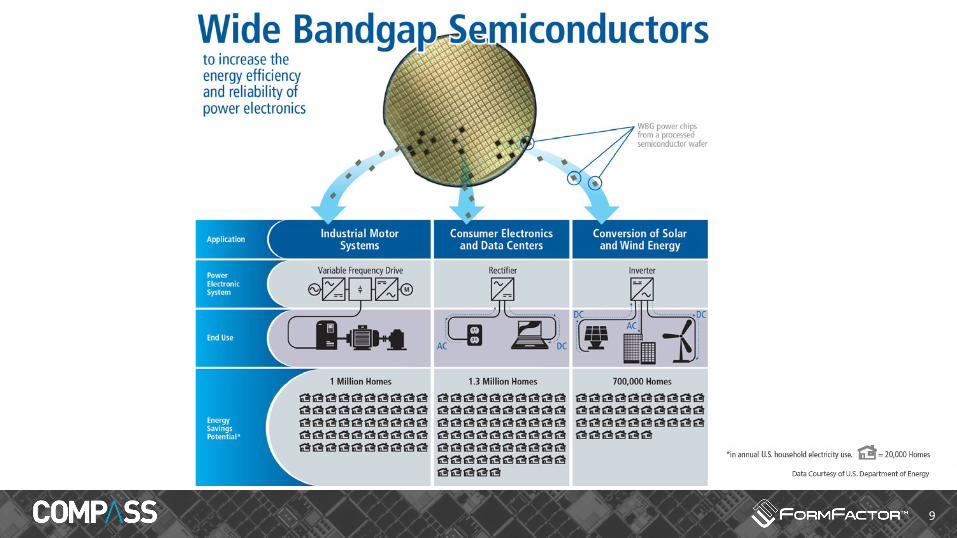
Power Semiconductors (Applications and Technologies)

77
Power Semiconductors (Applications and Technologies)

88
GaN / SiC Technology in the real world
GaN / SiC Devices Technology benefit Applications
Devices can be smaller Smaller packaging into consumer products
Devices can support higher temp
Increaser reliability in Automotive EV
Devices are more efficient (higher switching speed)
Lower energy loss / heat in industrial uses
99

1010
• On-wafer measurements reduce:• eng design cycle time • eng design cycle packaging costs• mfg packaging costs (only KGD)• mfg packaging time (only KGD)• delayed time-to-market for new products
Design Wafer Fab Parametric Test Sort Test Final TestPackaging KGP
Design Wafer Fab Parametric Test Chip Sort Test Packaging Final TestKGD
Package and Test process
Package vs On-Wafer

1111
On-wafer High Power Test
• Industry Needs• Material Characterization: SiC, GaN, Si, and SOI versions • Device Characterization: on-wafer accuracy (SiC, GaN, Si)• Reliability tests - higher operating V / I, higher temps • Commercial: reduce Cost Of Test (pkg to wafer) • Production prober for “Specialty high perf. devices”
• Key on-wafer Measurement Needs• Accurate/consistent Rds data on Single / Volume wafers• Full temperature support -55….+300/400oC• Voltages up to 10kV DC, Currents up to 600A• Support for engineering probes AND probe cards• Easy setup for lateral and vertical devices• Safe thin wafer autoloading • Low Inductance for dynamic power tests
DIODE

1212
Wafer-Level Test Challenges
• Safety for operator and system• System isolation for high voltage applications• Low resistance contacts and path for high current
applications (chuck & probe tips)• High-voltage arcing• Thin-wafer handling• Integration of different measurement instruments
with emphasis on measurement accuracy and safety requirements
• High temperatures• Low inductance for high switching speeds

1313
Automated probe cleaning
Precision wafer stage – 2x faster
Auto Wafer loader (4,6,8”) enables testing 50 wafers with 2nd Cassette
Next generation MicroChamber and easy access Top-hat covers
Small footprint
Modular Semi /Full-auto upgradeable
Thin/warped wafer handling (50um) with top-lift end effector
New manual hot wafer unload/load
New high performance eVue 4 Digital imaging system, and programmable
microscope travel increase die-to-die test speed
New Velox software with easy operation "Guided mode” (version 2.3)
Easy MicroChamber / wafer access
Multi-speed manual XY controls
TESLA200Power Semiconductor
Probing System
Wafer Quick Access Port for increased throughput
Specialty chucks for +400oC, and low inductance/Cap(res) for UIS
Integrated High Thermal Stability (HTS) for enhanced probe contact
Patented TESLA Chuck Technologies• FemtoGuard Triax• Coax, and High Current • 3kV low cost versions • Wide temp -55..+300oC
Up to 10kV / 600A with thin-wafer loadingAccurate Rds(on) with constant Rc at ALL temperatures with Contact Intelligence
Anti-arcing solutions for wafer and probes
TUV certified high power safety enclosure
Integrated vibration isolation & system electronics

1414
TESLA Probing System Solutions
High-Current Probes
High-Power Probes High-Voltage
Probes
2
High Voltage Chuck Port
ConnectionPackages5 High
Voltage MicroVac Triax
Chuck with
1

1515
Probing Challenge: Measuring Rds(on) for Vertical Devices
Chuck
Rc = Contact Resistance
Rds
SOURCE
DRAIN
GATE
Device
High CurrentForce Sense
ChuckSense
ChuckForce
Need high-current pulse on the source/drain Need Kelvin measurement capability Backside drain/source require minimal contact
resistance (Rc) between the wafer and chuck for accurate Rds(on) measurement Need wafer Rc uniformity for accurate device
statistical data

1616
Low Resistance wafer contact (Rc)
• Tesla chucks with MicroVac• Patented technology• 2nd generation version for thinned wafers• Stronger vacuum system for uniform wafer “hold down”• Uniform low contact resistance • BENEFIT: More accurate test data
TESLA MicroVacTriax chucks
2nd Gen. MicroVac Triaxchucks
Chuck Surface Flat Flat
Plating Gold (Au) Gold (Au)
Vacuum System Standard Next Generation
Vac. holes 495 495
Hole size 400um 200um
Supply channel Standard Flow optimized
Tyco support Yes Yes
Tyco vacuum Reduced Full

1717
Case Study: Package vs On-wafer + low Rc wafer chuck

1818
Probing Challenge: Low Leakage Measurements at HV
Situation Engineers need to understand device leakage current behavior at high voltages.
Solution TESLA200 provides a patented High Power triaxial chuck system for measuring leakage levels as low as 10fA.
Benefits Helps engineers understand their devices leakage behavior for currents under the 10 pA range and to increase the application value of their devices

1919
High-Voltage Chuck Port (Patent Pending)
Shield
Guard
Force &Sense
Interlock SwitchTesla Chuck
Interlock connectionFront View
Back View
• Chuck side connector:• 3 kV Triax, 10 kV Coax• Force and Sense connection, Femto Amp leakage• direct connection to service loop, sits on bridge, easily accessible• Interlock connection of safety

2020
High-Voltage Chuck Connection Cable
Shield
Guard
Force &Sense
Front View Safety shield
• Instrument side connector:• 3 kV Triax , 10 kV Coax (max), voltage rating depends on end connector• Force and Sense connection• Available end connector: HV Triax, Std Triax, CMI Triax, BNC, Banana, SHV• Shorting and Floating plugs• Interlock connection of safety
2121
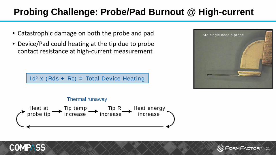
Probing Challenge: Probe/Pad Burnout @ High-current
Heat at probe tip
Heat energy increase
Tip R increase
Tip temp increase
Thermal runaway
Std single needle probe
Id2 x (Rds + Rc) = Total Device Heating
• Catastrophic damage on both the probe and pad• Device/Pad could heating at the tip due to probe
contact resistance at high-current measurement

2222
Solution: Reduce probe contact resistanceTypical Scrub Mark
on Aluminum Pad
High Current Probe
(3 fingers)
• Tesla’s HCP high current Probe• Novel Multi-finger design
• Reduced contact resistance• Good distribution of current• Minimal pad damage• Emulate Multiple bond wires
• Suitable for all pad material (tungsten tips)
• Replaceable Probe Tips• Up to 10A DC/60A Pulsed (1ms)
Typical scrub mark on Al Pad

2323
Probing Challenge: Utilizing test equipment on-wafer
• Ultra High Voltage / Current• Keysight B1505A Power Device Analyzer 3KV/40A• Keysight N1265A UHC Expander/Fixture 600A*• Keysight N1268A UHV Expander 10KV• Requires N1254A-524 (Prober Interface)
UHVE N1268A B1505A UHCE N1265A

2424
Extended Current Capabilities
• Complete Probe Solutions covering entire 10kV / 600A measurement range

2525
Extended Current Capabilities / Integration

2626
3KV, 300A Lateral Connection diagram

2727
Probing Challenge: Increase HC/HV test throughput
• Reduce test time to measure both high voltage and high current on the same device• Reduce setup time (HV & HC)• Reduce time / errors with potential die mismatching

2828
Solution: UHP Probe
A single probe to use in both high-voltage and high-current applications – no need to change probes and measurement setups
• Up to 300 A per probe (thus 600 A by a pair) or 10 KV on one probe
• Minimal damage to the wafer due to probing• High-current testing needs high probe forces to
reduce contact resistance• Special tip shape, pad penetration is minimal

2929
Solution: UHP Probe
Higher test throughput via reduced testing time• Up to 100% throughput improvement when reducing two wafer runs to one• Additional savings by one setup only

3030
Probing Challenge: Using HV Probe cards without arcing
• Solution with TESLA200 and T.I.P.S HV probecards
T.I.P.S.Probe Cards
Non-thermal Engineering High Temp
Production High Temp
Max Voltage 10,000V 10,000V 10,000V
Max temperature 85oC 200oC 150oC
Anti-arcing pressure chamber
Yes Yes Yes
Air seal to wafer Hovering (~80um gap)
Contacting Hovering (~80um gap)
Pressurized chamber with one needle

3131
Cambridge University Case Study – Before
• No thermal capability• Upper voltage limited by safety
concerns• No ability to measure substrate
currents accurately• Upper current capability limited by
probe and station service loop• Not possible to switch from High
voltage low current to High current low voltage for Current Collapse measurements
• Manual
3232
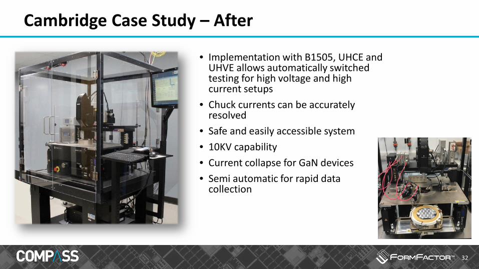
Cambridge Case Study – After
• Implementation with B1505, UHCE and UHVE allows automatically switched testing for high voltage and high current setups
• Chuck currents can be accurately resolved
• Safe and easily accessible system• 10KV capability• Current collapse for GaN devices• Semi automatic for rapid data
collection

3333
Current collapse measurements
• In some devices, the on state Ron resistance is degraded, after a high voltage Vdd has been applied in the ‘off’ state
• Device recovers to expected values, but takes time after going into on state• Measuring this transition is of interest

3434
N1267A Fast Switch – Current Collapse Measurements

3535
Current collapse measurements
3636
Summary
• Applications using Power Semiconductors see continual strong growth• GaN and SiC devices enable increased performance over Si• On-wafer testing of GaN & SiC devices have additional challenges for
• Higher Voltage / Current• High temperature• Switching speed
• TESLA200 provides complete solution • for high power GaN, SiC, & Si device testing @ temperature• with seamless integration with UHV / UHC implementations from Keysight• and safe, accurate, device data collection

3737
Thank You