our notre rdltl/l'fico - mcgill universitydigitool.library.mcgill.ca/thesisfile26418.pdf · a...
TRANSCRIPT

1+1 National Libraryof Canada
Bibliothèque nationaledu Canada
Acquisitions and Direction des acquisitions etBibliographie SelVices Branch des services bibliographiques
395 Wellington StreetOttawa, OntarioK1AON4
NOTICE
395. rue WellingtonOnawa (Ontario)K1A ON4
Yoor /lit) VoUt! IOftlroncC
Our 11/0 Notre rdltl/L'fICO
AVIS
The quality of this microform isheavily dependent upon thequality o~ the original thesissubmitted for microfilming.Every effort has been made toensure the highest quality ofreproduction possible.
If pages are missing, contact theuniversity which granted thedegree.
Some pages may have indistinctprint especially if the originalpages were typed with a poortypewriter ribbon or if theuniversity sent us an inferiorphotocopy.
Reproduction in full or in part ofthis microform is governed bythe Canadian Copyright Act,R.S.C. 1970, c. C-30, andsubsequent amendments.
r-"'".. - d···\ ....d.ua a
La qualité de cette microformedépend grandement de la qualitéde la thèse soumise aumicrofilmage. Nous avons toutfait pour assurer une qualitésupérieure de reproduction.
S'il manque des pages, veuillezcommuniquer avec l'universitéqui a conféré le grade.
La qualité d'impression decertaines pages peut laisser àdésirer, surtout si les pagesoriginales ont étédactylographiées à l'aide d'unruban usé ou si l'université nousa fait parvenir une photocopie dequalit~ inférieure.
La reproduction, même partielle,de cette microforme est soumiseà la Loi canadienne sur le droitd'auteur, SRC 1970, c. C-30, etses amendements subséquents.

•
•
•
A Performance Comparison ofSwitched-Current Structures
Peter M. K. SinnB.Eng.(Hon) 1991
McGill University, Montreal
November 1994
A Thesis submitted to the Faculty of Graduate Studies and Research in partialfulfillment of the requirements for the degree of Masters of Engineering.
© Peter M. K. Sinn 1994
. ;.

••• National Ubraryof Canada
BibliothèQue nationaledu Canada
Acquisitions and Direction des acquisitions etBibliographie Services Branch des services bibliographiques
395 Wellington Street 395, rue WellingtonOttawa, Ontario Ottawa (Ontario)K1AON4 K1AON4
l'OUf flle Vot/ll rd/6rffflC6
Our 1,/6 NoUe réloronce
THE AUTHOR HAS GRANTED ANIRREVOCABLE NON-EXCLUSIVELICENCE ALLOWING THE NATIONALLffiRARY OF CANADA TOREPRODUCE, LOAN, DISTRIBUTE ORSELL COPIES OF mSIHER THESIS BYANY MEANS AND IN ANY FORM ORFORMAT, MAKING TffiS THESISAVAILABLE TO INTERESTEDPERSONS.
THE AUTHOR RETAINS OWNERSffiPOF THE COPYRIGHT IN mSIHERTHESIS. NEITHER THE THESIS NORSUBSTANTIAL EXTRACTS FROM ITMAY BE PRINTED OR OTHERWISEREPRODUCED WITHOUT mSIHERPERMISSION,
L'AUTEUR A ACCORDE UNE LICENCEIRREVOCABLE ET NON EXCLUSIVEPERMETTANT ALA BffiLIOTHEQUENATIONALE DU CANADA DEREPRODUIRE, PRETER, DISTRIBUEROU VENDRE DES COPIES DE SATHESE DE QUELQUE MANIERE ETSOUS QUELQUE FORME QUE CE SOITPOUR METTRE DES EXEMPLAIRES DECETTE THESE ALA DISPOSITION DESPERSONNE INTERESSEES.
L'AUTEUR CONSERVE LA PROPRIETEDU DROIT D'AUTEUR QUI PROTEGESA THESE. NI LA THESE NI DESEXTRAITS SUBSTANTIELS DE CELLECI NE DOIVENT ETRE IMPRIMES OUAUTREMENT REPRODUITS SANS SONAUTORISATION.
ISBN 0-315-99980-2
Canad~

•
•
Abstract
ln 1989 a new analog IC sampled-data circuit technique was proposed called theSwitched-Current (SI) technique. Unlike other IC circuit techniques, the SI techniquecan realize analog functions using only MOS transistors without the need of anyresistor, capacitor or other linear component. This is beneficial to the IC communityat large, as mixed-signal IC's can now be realized using a standard digital CMOSprocess. SI circuits are dassified into two groups: first or second-generation, dulynamed to correspond to the time of their introduction. On account of circuits thathave been proposed over the past five years, this thesis will attempt to determinewhich circuits are better and what design strategy IC designers should follow whenworking with SI circuits.
Specifically, this thesis will investigate the linear and non-linear behaviors of thevarious SI circuits using a relatively new frequency-domain analysis technique. Thetransient behavior of an SI circuit subjected to a sinusoidal excitation is first computed using HSPICE. The output signal is then post-processed using a Fast FourierTransform from which the Power Spectral Density is found. Subsequently, both thelinear and non-linear circuit errors are determined. This analysis procedure is appliedto several basic first and second-generation SI structures, induding the memory cell,delay cell and integrator. Our results reveal that second-generation circuits generatelarge levels of signal distortion on account of a. serious glitching problem inherent withthese circuits. While in sorne cases, the situation can he improved by sophisticatedcircuit structures and modified dock schemes, the behavior of second-generation SIcells and circuits are, in general, outperformed by their first-generation counterparts.
Finally, to verify the above simulation results, two second-order SI filters weredesigned, laid-out and fabricated using first and second-generation cells in a 1.2 jlmCMOS process. The filters weredesigned to operate on a 5V power supply andeach occupied approximately the same amount of silicon area at 2300jlm x 1450jlm.Unfortunately, experiments with the returned IC's from fabrication revealed 11 designerror. Nonetheless, the design description provided here will serve as a useful guidelinefor others embarking on SI circuits.

•
•
.'
Resumé
En 1989 une nouvelle technique pour circuit intégré (CI) à échantillonage a été introduite et nommée Échantillonage Périodique du Courant sur des Intervalles l"ixesde Temps (EPCIFT). Contrairement à d'autres techniques pour CI, l'EPCIFT peutréaliser des transformations analogiques à l'aide seulement de transistors MOS, sansavoir recours à des résistances, condensateurs ou autres éléments linéaires. Ceci estun pas en avant pour le domaine des CI puisque des circuits à signaux mixes peuvent maintenant être réalisés par un processus de fabrication CMOS digital. Lescircuits EPCIFT sont rangés dans deux catégories: première ou deuxième génération,intitulées ainsi d'après leur ordre d'apparition. Sur la base des circuits proposés aucours des cinq dernières années, ce mémoire tente de déterminer quels circuits sontsupérieurs et quelles stratégies sont bénifiques aux créateurs de circuits EPCIFT.
En particulier, ce mé,TIoire examinera les comportements linéaire et non-linéairedes différents circuits EPCIFT en utilisant une technique d'analyse spectrale encore peu utilisée. La réponse en temps réel d'un circuit EPCIFT excité par uneonde sinusoïdale est d'abord calculee J. l'aide d'HSPICE. Le signal de sortie est alorstraité à l'aide d'une transformation de Fourier accelérée pour en obtenir la densitéspectrale. Par la suite, les erreurs linéaires et non-linéaires dit circuit sont obtenues.Cette procédure est appliquée à plusieurs structures EPCIFT de première et deuxièmegénération incluant les structures de mémoire, de délai et d'intégration. Nos résultatsdémontrent que les structures de deuxième génération produisent un niveau importantde distortion, dû a un problème sérieux de sursauts de courant inhérent à ces circuits.Alors que dans certaines conditions, la situation peut être améliorée par l'usage detechniques sophistiquées de circuits ou par la modification du système d'horloge, lesstructures de première génération produisent généralement de meilleurs résultats queleurs équivalents de deuxième génération.
Finalement, pour vérifier les résultats de simulations cités ci-haut, deux filtres EPCIFT de deuxième ordre ont été conçus et fabriqué à partir de structures de premièreet deuxième génération sur un processus CMOS de 1.2j.tm. Les filtres furent conçuspour opérer à partir d'une tension de 5V et occupent chacun approximativement la
11

•
•
•
même surface de silicium, soit 2300iLm par 1450iLm. Malheureusement, les expériencessur les Cl obtenus ont révélé une erreur de conception. Malgré tout, les descriptionsde circuits incluses serviront de guide utile pour les concepteurs de circuits EPCIFT.
111

•
•
•
Acknowledgements
l would like to take this opportunity to thank my supervisor, Prof. Gordon W.
Roberts for his unfailing guidance throughout the course of this research. His fre-•
quent availability and invaluable advice are the core to the success of this wode
l would also like to thank my colleagues, in particular, Ml'. Phil Crawley for the
enlightenment in SI circuit design issues through numerous discussions, Ml'. .h\cck
Slaboszewicz and Ml'. Charles Arsenault, the system administrators, who perfected
the computer system in MACS Lab and Dr. 1. Shih for his generosity fol' the use of the
micro-photographie equipment. Thanks also go to National Scientific and Engineet·
ing Research Council (NSERC) and Canadian Microelectronics Corporation (CMC)
from which most of the funding for this work cornes.:
l also want to express my sincere thanks to Fr. Thomas Tou for providing acco
modation throughout my stay in Montreal. Gratitude also goes to my fricnds who
provided many exciting times for me in and outside my alma matcr. l must also mcn
tion my parents, my brother, Tony, and my sister, Cathcrinc, fol' al! thcir support,
patience and sacrifice throughout the work of my bachelor and master dcgrccsj and
also to Vivian who went through ail the ups and downs with me. Last but Ilot least,
l thank God for granting me my life and my wisdom and may He lead me at this
beginning of a new era in my life.
iv

•
•
•
Contents
Abstract
Resumé
Acknowledgements
1 Introduction
1.1 Review of the SI Technique .
1.1.1 First-Generation SI Mernory Cell
1.1.2 Second-Generation SI Mernory Cell
1.2 Motivation ...
1.3 Thesis Outline .
2 Nonideal Memory Cell Behavior
2.1 Cornrnon Errors of First and Second Generation Cell
2.1.1 Settling Tirne Errol' . . .
2.1.2 Charge-Injection Effect .
V
i
ii
IV
1
3
3
6
7
8
11
12
13
17

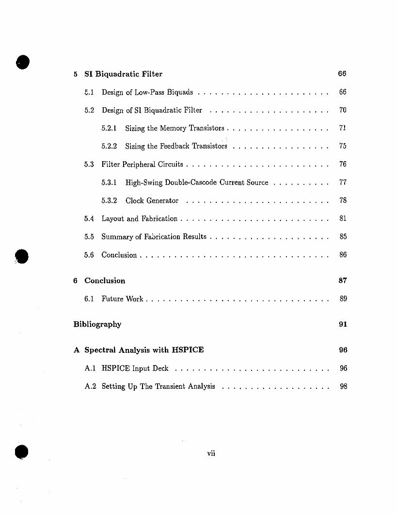
• 5 SI Biquadratic Filter 66
5.1 Design of Low-Pass Biquads 66
5.2 Design of SI Biquadratic Filter 70
5.2.1 Sizing the Memory Transistors . 71
5.2.2 Sizing the Feedback Transistors 75
5.3 Filter Peripheral Circuits . . . . . . . . 76
5.3.1 High-Swing Double-Cascode Current Source 77
5.3.2 Clock Generator 78
5.4 Layout and Fabrication. 81
5.5 Summary of Fa~rication Results . 85
• 5.6 Conclusion. . . . . . . . . . . . . 86
6 Conclusion 87
6.1 Future Work . ............................... 89
•
Bibliography
A Spectral Analysis with HSPICE
A.l HSPICE Input Deck . . . . . .
A.2 Setting Up The Transient Analysis
vii
91
96
96
98
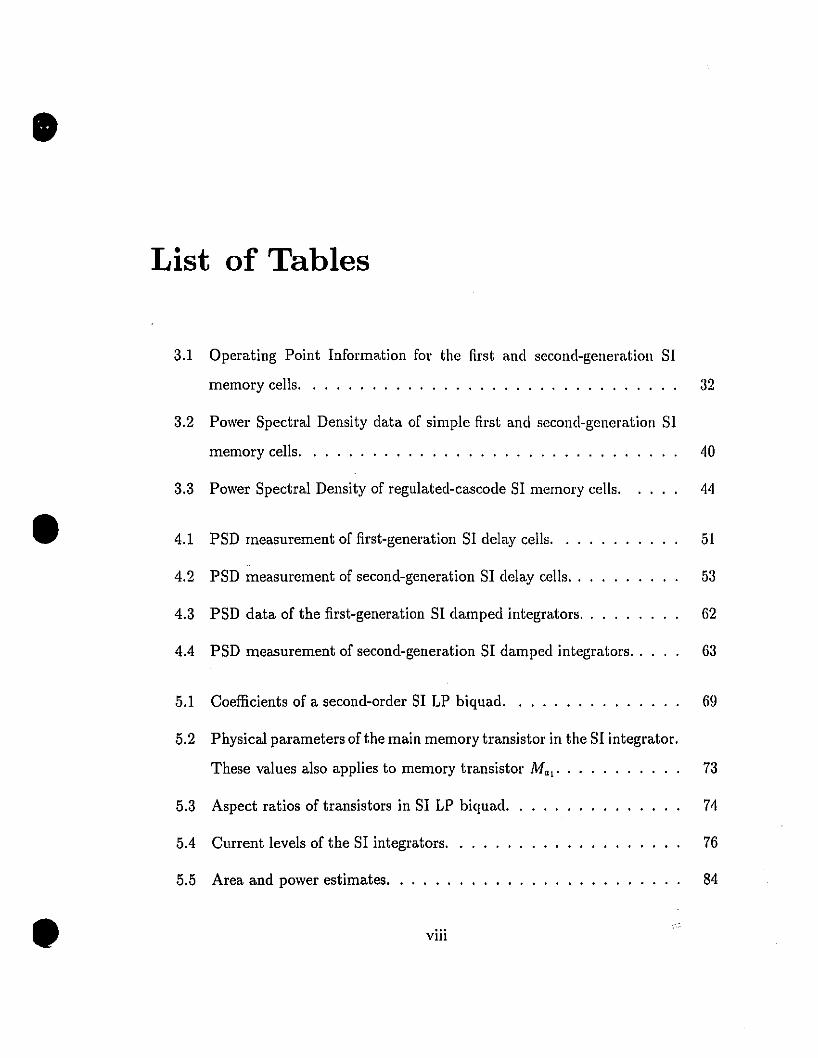
•List of Tables
3.1 Operating Point Information for the first and second-generation SI
memory cens. . . . . . . . . . . . . . . . . . . . . . . . . . . . . . 32
3.2 Power Spectral Density data of simple first and second-generation SI
memory cens. . . . . . . . . . . . . . . . . . . . . . . . . . . . 40
3.3 Power Spectral Density of regulated-cascode SI memory cens. 44
• 4.1 PSD rneasurement of first-generation SI delay cens. . .
4.2 PSD measurement of second-generation SI delay cens..
51
53
4.3 PSD data of the first-generation SI damped integrators. . 62
4.4 PSD measurement of second-generation SI damped integrators. . 63
5.1 Coefficients of a second-order SI LP biquad. . . . . . . . . . . . . .. 69
5.2 Physical parameters ofthe main memory transistor in the SI integrator.
These values also applies to memory transistor Mal' 73
5.3 Aspect ratios of transistors in SI LP biquad. 74
5.4 Current levels of the SI integrators. 76
•5.5 Area and power estimates. . . . . .
viii
84

•
•
List of Figures
1.1 First-generation SI memory cell. . . . . . . . . . . . . . . . . . . . " 4
1.2 Switching waveforms of (a) first-generation and (b) second-generation
SI memory cell. . . . . . . . . . . . 5
1.3 Second-generation SI memory cell. . 6
2.1 (a) First generation SI memory cellj (b) Small-signal equivalent circuit
in charging phase; (c) small-signal equivalent circuit in memorization
phase. . " 14
2.2 (a) Second generation SI memory cell; (b) Small-signal equivalent cir
cuit in charging phasej (c) small-signal equivalent circuit in memoriza-
tion phase. . . . . . . . . . . . . . . . . . . . . . . . . . . . . . . . " 16
2.3 Charge-injection effect on SI memory cells: (a) charge tlQ stored in
the channel when the switch is ON; (b) charges escape through the
switch terminaIs when the switch is turned OFF. 18
2.4 Different schemes for cancellation of channel charge-injection: (a) CMOS
transmission gate, (b) dummy switch, and (c) extra circuit to counter-
act charge-injection. 20
•2.5 Schematic illustrating fini te input and output conductances.
ix
21

•
•
•
2.6 The first and second-generation SI memory cells showing their struc-
tural similarity when gain other than unity is concerned. . . . . . .. 23
2.7 Describing the phenomenon of variation of input-impedallce level: (a)
second-generation SI memory cell with simplified switches, (b) during
the chal"9ing phase: SI and S2 are both ON, node C is low-impedancej
(c) before the memorization phase: S2 and S3 are opened when SI is
still ON, node C changes ta high-impedance. . . . . . . . . . . . . o. 25
3.1 Schematics of SI memory cells for HSPICE simulation put'pose: (a)
first-generation and (b) second-generation. Notice the extra swikh at
the input of the second-generation memory cell is required to provide
a signal path to ground. 30
3.2 Simple two-phase non-overlapping dock scheme used for the first and
second-generation current memory cells. 31
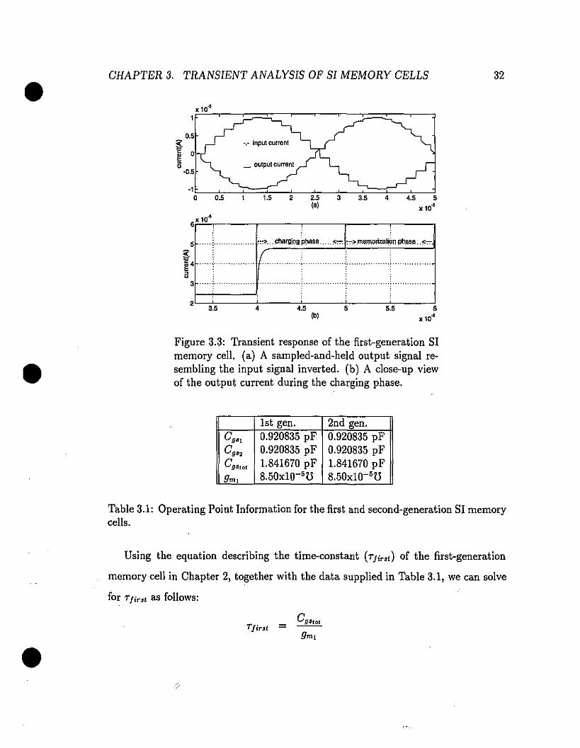
3.3 Transient response of the first-generation SI memory cell. (a) A sampled
and-held output signal resembling the input signal inverted. (b) A
dose-up view of the output current during the charging phase. 32
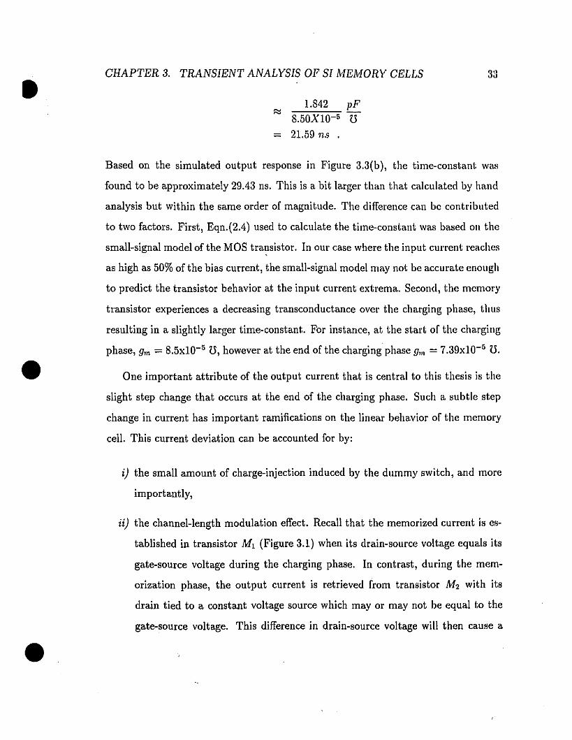
3.4 Simulated transient responses of the second-generation memory cell
highlighting the glitching problem: (a) the mirrored output 1o"" and
(b) the direct output 10d' •••••••••••••••••••••••• 34
3.5 (a) settling behavior of the mirrored output current of the second
generation SI memory cellj (b) the corresponding input node-voltage,
Va. . . . . . . . . . . . . . . . . . . . . . . . . . . . . . . . . . . . .. 36
3.6 Proposed modified 3-phase dock scheme ta reduce glitching effect in
the second-generation memory cell. . . . . . . . . . . . . . . . . . .. 38
x

• 3.7 Improved transient response of the second-generation memory ceIl with
the modified dock scheme incorporated: (a) mirrored output and (b)
direct output. . . . . . . . . . . . . . . . . . . . . . . . . . . . 39
3.8 A regulated-cascode super-transistor and its equivalent circuit. 41
3.9 Regulated-cascode version of SI memory ceIls: (a) first-generation, (b)
second-generation. 43
•
3.10 Transient responses of the regulated-cascode version of (a) the first
generation memory ceIl; (b) mirrored output of second-generation mem-
ory ceIl and (c) corresponding direct output. . . . . . . . . . . . . .. 45
4.1 SI delay cel! formed by cascading two memory ceIls: (a) first-generation
and, (b) second-generation. . . . . . . . . . . . . . . . . . . . . . . .. 48
4.2 Time-domain transient responses of the first-generation delay ceIl with
and without the regulated-cascode configuration. Identical responses
in each case. . . . . . . . . . . . . . . . . . . . . . . . . . . . . . . .. 50
4.3 Transient response of the second-generation simple SI delay ceIl from:
(a) direct output, and (b) mirrored output. . . . . . . . . . . . . . .. 52
4.4 Transient response of the second-generation regulated-cascode SI delay
ceIl from: (a) direct output, and (b) mirrored output. . . . . . . 54
4.5 First-Generation SI Integrator...
4.6 Second-Generation SI Integrator.
55
57
•4.7 SI Damped Integrators formed by an additional feedback loop: (a)
first-generation and (b) second-generation. . . .. . . . . . . . .. 58
xi
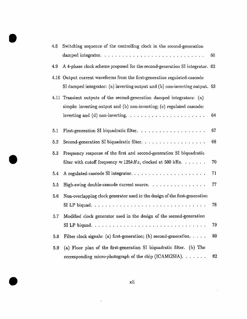
• 4.8 Switching sequence of the controlling dock in the second-genel'atioll
damped integl'atol'. . . . . . . . . . . . . . . . . . . . . . . . . . . .. GO
4.9 A 4-phase dock scheme proposed for the second-generation SI integrator. 62
4.10 Output current waveforms from the first-generation regulated-cascode
SI damped integrator: (a) inverting output and (b) non-inverting output. 63
4.11 Transient outputs of the second-generation damped integratol's: (a)
simple: inverting output and (b) non-inverting; (c) regulated cascode:
inverting and (d) non-inverting. . . . . . . . . . . . . . . . . . . . .. 64
5.3 Frequency response of the first and second-generation SI biquadratic
filter with cutoff frequency ~ 125kHz, docked at 500 kHz. . . . . .. 70•5.1 First-generation SI biquadratic filter. .
5.2 Second-generation SI biquadratic filter.
67
68
5.4 A regulated-cascode SI integrator .
5.5 High-swing double-cascode current source.
71
77
5.6 Non-overlapping dock generator used in the design of the first-generation
SI LP biquad. . . . . . . . . . . . . . . . . . . . . . . . . . . . . . .. 78
5.7 Modified dock generator used in the design of the second-generation
SI LP biquad. . . . . . . . . . . . . . . . . . . . . . . . . . . .
5.8 Filter dock signais: (a) first-generation; (b) second-genel'ation.
79
80
•
5.9 (a) Floor plan of the first-generation SI biquadratic filter. (b) The
corresponding micro-photograph of the chip (ICAMGSIA). . . . 82
Xli
•
•
•
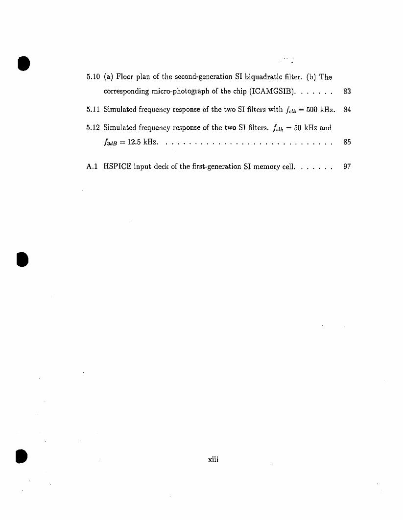
5.10 (a) Floor plan of the second-generation SI biquadratic filter. (b) The
corresponding micro-photograph of the chip (ICAMGSIB). . . . . .. 83
5.11 Simulated frequency response of the two SI filters with fclk = 500 kHz. 84
5.12 Simulated frequency response of the two SI filters. fclk = 50 kHz and
fadB = 12.5 kHz. 85
A.1 HSPICE input deck of the first-generation SI memory cell. . . . . .. 97
xiii
•
•
•
Chapter 1
Introduction
The role of an integrated analog circuit has changed dramatically in the past; decadc.
In past years, analog circuits were used in different sig,;al processing applications
which included filtering, decimation and interpolation, to namejust a few. In cont;rast,
today the signal processing operations that an analog circuit once performed are being
replaced by digital signal processing techniques. This is not to say that analog circuits
are no longer required in integrated form. On the contrary, analog circuits arc playing
an ever-increasing role at the interface between the digital circuits implementing t;ne
signal processing functions and the real-world. The net effect of this change is that the
amount of silicon area required to implement these remaining few analog operations
has decreased significantly. As an example a voice-band CODEC of the early SO's
consisted of 70% or more of analog circuits [1], with the l'est implemented with digital.
Today, we are seeing similar mixed-signal IC's with only 10% - 20% of its silicon area
occupied by analog circuits. Not surprising, when industry is faced with optimizing
their processes for maximum performance and yield, it is usually directed at the
digital portion of the mixed-signal IC at the detriment of the analog circuit.
The impact of this neglect can be seen directly on the Switched-Capacitor (SC)
1
• CIJAPTER 1. INTRODUCTION 2
•
•
circuit technique [2]. This technique has been the dominate analog circuit method
fol' fully-monolithic implementation since the early 80's. SC circuits are based on
moving charge packets between different capacitors in the circuit under the control
of a precise clock circuit operating various switches. An important technological
constraint of SC circuits is the requirement for linear capacitors [3J. In order to
accommodate such a requirement, a standard digital CMOS process must be modified
to include an additionallayer of polysilicon. This, however, brings no advantage to
the digital designs and consequently, increases the cost of the overall IC [4]. Besides
the economics, SC circuits do not lend themselves to shil'king power supply operation,
a necessary requirement for the further miniaturization of electronic systems. This,
in turn, poses additional difficulties in designing SC circuits as the available voltage
headroom for output swing is also reduced accordingly with power supply reduction.
Although effort has begun investigating ways in which to implement SC circuits on
low power supply levels, for example on operating a SC circuit on a 3.3 V supply [5],
it is not clear how these circuits will operate on lower supply levels such as those used
in battery powered systems (Le., 1 V). With the availing degradation in performance
and the cost of implementing an addition polysilicon layer in an otherwise standard
digital CMOS process, the SC technique becomes less and less attractive.
ln 1989, Hughes et al [6] proposed an innovative circuit design technique that can
provide accurate signal processing without the use of any linear capacitor. Rather, it
uses the non-linear gate-source capacitance of a MOS transistor to store information.
This, of course, allows SI circuits to be implemented in a low-cost standard digital
CMOS process. This technique is named as the Switched-Current technique, or SI
technique for short. At about the same time Daubert et al [7] proposed a similar
technique but referred to it as the Current Copier technique. In this work we shaH

use the term Switched-Current to refer to these circuits. Another advalltage of SI
circuits is that the resulting circuits are usually much simplier and less power-hungry
[8, 9]. Simple circuits should also allow for faster operation as less capacitanœ is
resident in the circuit. Ano.ther important advantage of SI circuits is the faet that
they process input information in the form of a current and it is expected that sllch
circuits would be less affected by power supply reduction. Effort is presently lInderway
investigating this aspect of SI circuits [10], as sorne SI circuits do not have this ability.
In the end, the cost of manufacturing mixed-signal IC's will be noticeably reduced
with the introduction of the SI technique.
• CHAPTER 1. INTRODUCTION 3
•
•
1.1 Review of the SI Technique
The basic circuit element of the SI technique is the currenl memOl'y cell. As the
name suggests, the memory cell stores a current in the form of a charge stored on
the gate-source capacitance of a MOS transistor. Two different types of this circuit
have emerged since the introduction of the SI technique, duly labeled as the first and
second-generation current memory cell, to correspond to the time of their introduction
[6), [11]. AIthough different forms of cascoding and active feedback have been applied
to improve their operation, they can still be referred to as first or second-generation
type cells.
1.1.1 First-Generation SI Memory Cell
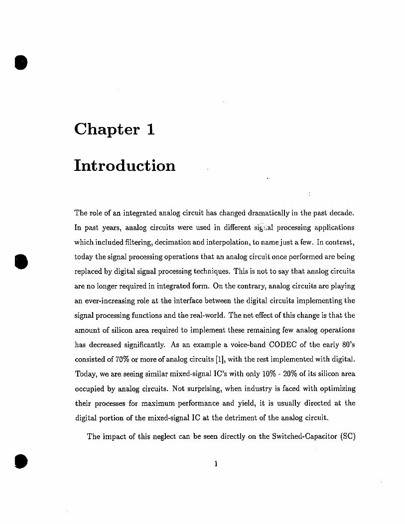
A first-generation current memory cell is shown in Figure 1.1. It resembles the
configuration of a simple current mirror with an extra transistor (Sd between the
gates of the two transistors (Ml and M2 ). Transistor St, which is usually smaller in
• CHAPTER 1. INTRODUCTION
A-,,
:~: CglJ !,,,,_.-
,,GgIJ';l :;:,,,,_.-
.-----0 Jout-
4
•
•
Figure 1.1: First-generation SI memory cell.
size compared to the other two, acts as a switch governed by the switching waveform
shown in Figure 1.2(a).
The operation of the first-generation cell is as follows: an input current-summing
node (A) is established by virtue of the diode-connected transistor MI, This low
impedance node receives the sum of the input and bias currents (lin and h) and in
turn causes the gate-source capacitance Cgs of MI to charge up to the appropriate
voltage level governed by the transistor V-I relationship. When switch SI is closed,
the gates of MI and M2 are connected together and the charge stored on the gate
capacitance of each transistor redistributes themselves among Cgs1 and Cgs2 in an
appropriate way. A current of magnitude p'-(I;n + lb) will then flow into the drain
of M2, resulting in an output current of lout2 = p,-lh - (h + lin)] = -p'-lin' where
AI and A2 denote the aspect ratios of transistors MI and M 2 , respectively. When
switch SI is opened, the two transistors are disconnected and the charge stored on
Cgs2 remains unchanged. Consequently, the same drain current flows in M2 keeping
lotit constant for the duration the switch remains open. On account of the fact that
the gate-source capacitance only holds a charge and do not participate in the linear

CHAPTER 1. INTRODUCTION 5• ON(S,,4» J \ 1 l OFF
(a)
ON~'.:
(SI or S" 4>1~ \i J l OFF, ,, ,(S" 4>,) \
1: \ r(b)
•Figure 1.2: Switching waveforms of (a) first-generation and (b) second-generation SImemory cell.
charge transfer process, these capacitances can be non-Iinear. In fact, they can be
implemented directly using the parasitic capacitance of the MOSFET and no other
external capacitor is required. Mathematically, the input-output current operation of
the memory cell can be described by the following expression
(1.1)
Performing the Z-transform on Eqn.(1.1) and re-arranging the expression, we can
write the transfer function for the memory cell as
(1.2)
•Besides the normal operation that a current mirror is capable of performing, such
as inversion and scaling, Eqn.(1.2) also demonstrates that the current rnemory cell
• CHAPTER 1. INTRODUCTION 6
-C91~ :~:,,,,
-"-
~ (S2,~tl
1f---I-: --- ----- ----- ---r-----1:;: Gg't,,,,-"-
B t-----,
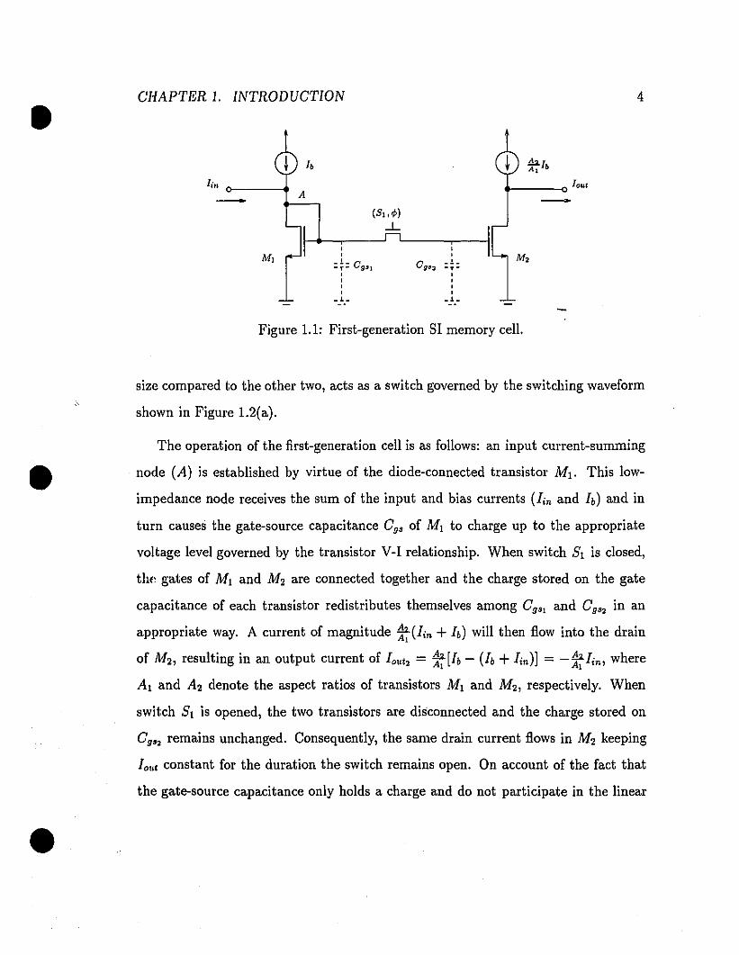
Figure 1.3: Second-generation SI memory cell.
•
provides a delay of half-a-dock period as indicated by the z-t term. One point worth
noticing is that the above equation represents the operation of the first-generation
SI memory cell as long as the output transistor M2 stays in saturation; otherwise,
undesirable non-linear operation will result.
1.1.2 Second-Generation SI Memory Cell
•
The second-generation memory cell shown in Figure 1.3 operates in a similar fash
ion as its first-generation counterpart. The main difference lies in the fact that only
one transistor partakes in its main operation and that a two-phase non-overlapping
dock scheme is required, as shown in Figure 1.2(b). Referring 1.0 Figure 1.3, during
the on-phase of <Ph switch S2 is dosed making MI diode-conneeted. In addition, SI
is also dosed allowing the input CUITent I;n and the bias current h 1.0 be summed al.
the low-impedance node B. The gate-source capacitance Cgs1 will then be charged
up by h + lin establishing a voltage according 1.0 Vas = Jlht{in +Vt, where f{ is a
function of the electron mobility and the transistor per-unit area capacitance, and Vt
is the threshold voltage of the MaS transistor. On dock phase <P2, when switch S3 is

elosed and 81 and 82 are opened, the charge stored on Cg" creates the same voltage
Vas, and the same drain current will continue to flow in Ml, In tUl'll, this will cause
a current equal and opposite to the input current half-a-period eartier to be pulled
from the output node of the memory cell, resembling the case of the first-generation
memory cell. This operation can again be described by Eqn.(1.1) but WiUl the nüio
~ equal to unity since there is only one transistor involved. To obtain current gain
other than unity, a current mirror circuit is established between the main memory
transistor MI and another transistor, such as transistor 1\12 shown in Figll1'e 1.3.
With proper scaling of the bias current, a scaled version of the input CUl'l'ent can be
obtained as Jout,.
• CHAPTER 1. INTRODUCTION ï
•
•
1.2 Motivation
Ever since the introduction of SI design techniques, there has been enormous discus
sion in the open research literature describing circuits that use the SI memory cell.
References [12, 13, 14] are illustrative of sorne of them. Systematic methodologies
outlining the design and synthesis of SI filters using presently existing SC designs
have also been proposed [8, 15]. Computer-Aided-Design tools such as ASIZ' and
WATSNAp2, although immature at the time of this writing, are also available to
assist designers in the analysis of SI circuits. Bearing the possibility of low-voltage
and low-power operation, together with compatibility with a standard digital CMOS
fabrication process, the SI technique is seriously being considered by industry as a
viable alternative to the SC technique.
On the other hand, however, the SI circuit technique has many unanswered ques
1ASIZ is a CAD tool for simulation of SI designs [16].2WATSNAP is a CAD tool developed by University of Waterloo for simulation of lineal' 8witched
system [17].
• CHAPTER 1. INTRODUCTION 8
•
•
tions that has slowed down its proliferation into commercial designs. To increase
its chances of success in industry, it is important to determine which SI circuits are
practical and which are not, and focus our remaining efforts on those that are prac
tical. To help us answer this question we went back to the basic circuits of the SI
technique and asked ourselves: Which cell type is better, first"generation or
second-generation? According to [11], the second-generation cell is believed to
possess a better sensitivity to component variations than the first-generation ceiP.
As a result, we see a lot of designers accepting this belief as recent trends seem to
suggest [13, 14J. However, as we gained more experience designing with SI circuits
[18J, we have come to the conclusion that circuits implemented with first-generation
memory cells are easier to work with and perform better than circuits implemented
using second-generation memory cells. It is therefore the intention of this thesis to
address this apparent dilemma by comparing the behavior of the first and second
generation structures and recommend to analog designers which is the better memory
cell.
1.3 Thesis Outline
Following this introduction, we will continue this thesis in Chapter 2 by outlining the
non-ideal behavior of the basic SI element - the SI memory cell. The errors which
arise from imperfections in the cell are categorized into common and specific errors.
Common errors are those that exist in both the first and second-generation cells while
specific errors appear only in a particular configuration.
In Chapter 3 a study of the non-linear behavior of the first and second-generation
memory cell is performed. Using the transient analysis capability of HSPICE com
"This will later he shawn in this thesis ta apply ooly ta sorne cell structures.

• CHAPTER 1. INTRODUCTION 9
•
•
bined with a Fast Fourier Transform (FFT) algorithm, the power spectral density of
the output response of each memory cell excited by a pure sinusoidal signal is derived.
Consequently, the harmonic distortion behavior of each memory cell is determined.
Here we will discover that the second-generation cell has a highly non-linear opera
tion. A circuit explanation is provided to account for this behavior. The remailling
portions of this chapter are focused on circuit techniques that improve the lineal'ity
of the two memory cells. Here we make use of new clock schemes and transistor
cascoding techniques.
Adopting a similar approach to that which used in the third chapter, Chapter il
performs a study of the non-linear behavior of delay and integrator cells cOllstructed
from first and second-generation cells. These cells arc important as they form the
basic building blocks of FIR and lIR filter circuits. Here wc will discover that delay
cells implemented with second-generation cells arc highly non-linear and that the
circuit techniques used to improve the operation of the second-generation memory
cell proposed in Chapter 2 do not hclp to improve its linear operation. In contrast,
the first-generation delay circuit has a much more linear behavior and its performance
can be further improved by transistor cascoding techniques. Although not as drastic,
similar conclusions apply to the integrator circuit. However, a four-phase clock scheme
or transistor cascoding techniques can be used to improve the linearity of the second
generation integrator cell.
Chapter 5 is devoted to the design of two second-order SI low-pass biquadratic
filters; one implemented with first-generation memory cells and the other with second
generation cells. The goal here is to experimentally validate the claims made in the
previous two chapters through simulation. Aiming to fabricate these filter circuits
using Northern Telecom Limited's 1.2 pm CMOS process, practical issues pertaining

to the sizing of transistor dimensions, clock design and current sources, will ail he
given in this chapter. Details on the floor plan of the lC will also he provided.
Subsequently, details on the operation of the lC's that have been returned from
fabrication will be given, together with the associated microphotographs.
Finally, in Chapter 6, conclusions are drawn and suggestions for future work are
made.
•
•
•
CHAPTER 1. INTRODUCTION 10
•
•
•
Chapter 2
N onideal Memory Cell Behavior
The operation of the Switched-Current memory cell was described in the previous
chapter. In doing so, we have subtly made the following assumptions:
i) the transconductance action of the cell is spontaneousj
ii) the transistor has an infinite input conductance and zero output conductance;
iii) the transition of the switches from ON to OFF and from OFF to ON are
instantaneousj
iv) the switch acts as perfect short- and opened-circuit during the ON and OFF
phases respectivelyj and,
v) there is no charge stored in the depletion region of the switch transistor when
the switch is ON.
This is certainly not the case in practical designs of Switched-Current circuits utiliz
ing the memory cell. In this chapter, we will outline sorne causes of non-idealities in
the cell. Since higher-order structures ail stem from the basic current memory cell,
it is believed that the non-ideal properties of the memory cell will he carried over
11

to aIl other SI circuits. Thus, a thorough understanding of these imperfections will
aid tremendously in designing SI circuits. The errors under consideration are catego
rized into common errors and specifie errors. Common errors which stems from the
forementioned non-idealities include the settLing error (result of item i and ii), switch
charge-injection error (result of item v) and finite input and output resistance error
(result of items iii and iv). AIl these errors appear to have almost similar effect on
the first and second-generation memory cell.
• CHAPTER 2. NONIDEAL MEMORY CELL BEHAVIOR 12
•
•
In addi tion to the common causes of errors, there are sorne sources of errors which
are ollly specifie to one cell type. A sensitivity problem to component mismatch was
thought to be present in first-generation structure but not the second-generation cell
as suggested by Hughes et al in [11]. We shall show later on in this thesis that this is
not necessarily true. On the other hand, the second-generation memory cell suffers
from a variation in the input-impedance level at the current summing-node which
creates large levels of signal glitching. This will be shown to be a limiting factor in
the cell's behavior.
2.1 Common Errors of First and Second Generation Cell
In this section, we will identify sorne of the common sources of errors of the first and
second-generation cells. Errors thus arisen will be discussed and where applicable,
mathematical expressions will be given to quantify the result.
• CHAPTER 2. NONIDEAL MEMORY CELL BEHAVIOR
2.1.1 Settling Time Error
13
•
The reaction of an SI circuit is not instantaneous. Intuitively, we will expect the circuit
to follow a first or second-order transient settling behavior owing to the distribution
of capacitances present in the circuit. The settling time is limited by the pel'iod of
the sampling dock which controls the switching. Thus, the settling behavior of the
circuit, which determines the time needed to obtain a particulaI' accuracy in the charge
transfer process, limits the frequency of operation of the circuit. In the following, a
small-signal analysis of the first and second-generation memory cell is undertaken.
First Generation Memory Cell: To illustrate the settling behavior of the first
generation memory cell, consider that the circuit of Figure 2.l(a) has two modes
of operation depending on the state of the switch. When the switch is dosed, the
equivalent circuit is that shown in Figure 2.1(b). This mode of operation is denoted
as the charging phase because this is when the input current is applied to the memory
transistor.
Now let us consider the effect that the input current i;n has on the output current.
According to straightforward circuit analysis using Laplace Transforms, the output
current iout(s) is given by
(2.1)
•
where Gl is the equivalent parallel conductance of the transconductance 9m, and
output conductance 90 1 of Ml correspondingly, Cl is the equivalent capacitance of the
gate-source capacitance Cgs1 and total drain capacitance Cdl of the same transistor.
Capacitor Cgs, is simply the gate-source capacitance of transistor M2 • Ali these small
signal parameters are assumed to be computed around the bias point of the memory

• CHAPTER 2. NONIDEAL MEMORY CELL BEHAVIOR 14
(a) iout-',op , G'l 1-~+ ,m"",! l 1
,lc,1 c,',1 '~"
•,o, _ cd"l
(b)
iout-+1,
,m,v",! l''''1
,l
V9.!2l 1Cd',
C,)
Figure 2.1: (a) First generation sr memory cell; (h) Small-signal equivalent circuit incharging phase; (c) small-signal equivalent circuit in memorization phase.
•
• CHAPTER 2. NONIDEAL MEMORY CELL BEHAVIOR 15
cell. For a step input of tli;n, the output CUITent can be computed from Eqn.( 2.1)
to be
(2.2)
where
(2.3)
•
•
Here we see that the charging phase is governed by a single-time-constant (STe)
charging process. With a properly designed circuit, the drain capacitance will be
small relative to the gate-source capacitance and Gl will be dominated by g"li as gOI
is very small. Thus, the time-constant is very weil approximated by
(2.4)
During the memorization phase when the switch opens, a charge is stored on the
gate-source capacitance of transistor M!. Its small-signal equivalent circuit is that
shown in Figure 2.1(cl. Since the output is taken through a constant voltage source,
or analog ground, the output conductance and capacitance are shorted out and have
no effeet on the charge transfer process. It is therefore fair to say that the output
charge transfer process is instantaneous. The value of i out will be the saIlle as the
value just before the switch is opened.
Second Generation Memory Cell: The second-generation memory cell without
an output mirror stage has a much simpler small-signal equivalent circuit as that seen
previously, as only one transistor partakes in the charge transfer process. If the mirror
stage is inc1uded, the exact same small-signal equivalent circuit drawn fol' the first
generation cell will then apply. Both of these situations are depicted in Figure 2.2(b)
with the dotted line indicating the optional choice of the mirrored output. Parameters
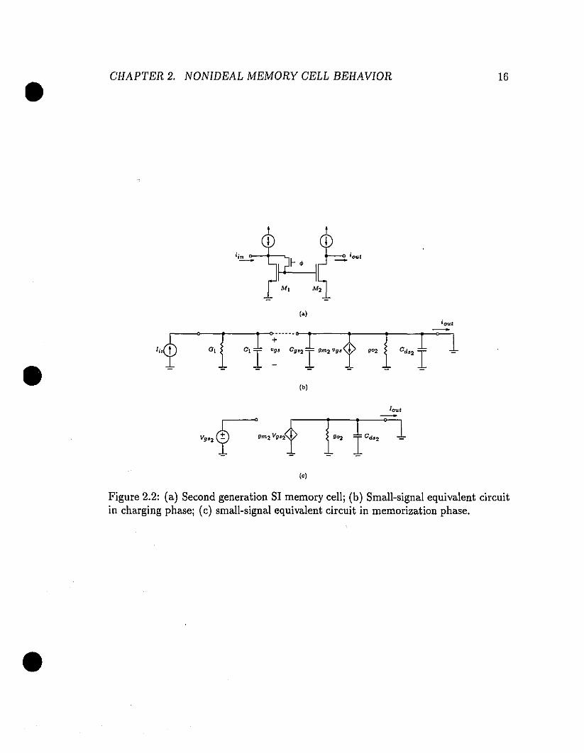
• CHAPTER 2. NONIDEAL MEMORY CELL BEHAVIOR
(a)
16
• (b)
Iout-1 '1l Cd., -
(,)
•
Figure 2.2: (a) Second generation SI memory cell; (h) Small-signal equivalent circuitin charging phase; (c) small-signal equivalent circuit in memorization phase.

• CHAPTER 2. NONIDEAL MEMORY CELL BEHAVIOR l7
G1 and Cl have the same meaning as previously stated. As was mentioned in the
introduction before, no mirroring action is required if current summation and CUITent
gain are not of concern. Thus, the small-signal m.:>del of the charging phase of the
second-generation memory cell reduces to a simple RC network with time constant """oG'1
which is very weil approximated by Gg.,. When arbitrary gain is desired, the modcl
Dml .
becomes exactly the same as that for the first-generation memory cell and the I;jme
constant of the circuit is equal to Tfirs! given in Eqn.(2.4). Mathematically, the time
constant of the second-generation memory ccII can be summarized as:
{~ ,
T - Dmlsecond - Cg./l! +C9 "2
Dml '
direct output
mirrored output(2.5)
•
•
2.1.2 Charge-Injection Effect
Another factor which contributes to the inaccuracy of the SI operation is the charge
injection effect related to the switches being used in the memory cell. Charge-injection
has been touted as one ofthe fundamentallimits of signal purity in SC circuits [19, 20]
and has been extensively studied in [21]. It is commonly believed that charge-injection
is also a major source of error in SI circuits. Although this is probably the case for
first-generation circuits, this thesis will demonstri,:.:' "hat a more dominant error is
present in second-generation cells - this being a s'.:lj,:d. glitching problem. It; will be
fully described in a later section. For the time being we shall describe the source of
charge-injection and its effects on SI circuits using a first-generation memory coll, sucb
as that shown in Figure 2.3. A similar description applies to the second-generation
cell.
Let us first consider that the switch of Figure 2.3 is in its ON-state. Thus in the
channel region a quantity of charge ÂQ is stored. Due to the presence of the biasing
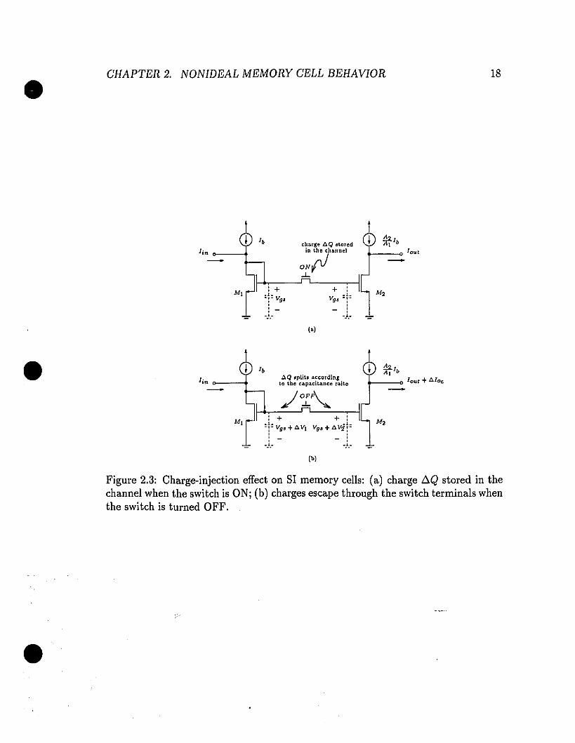
• CHAPTER 2. NONIDEAL MEMORY CELL BEHAVIOR 18
:+.,.-,- v:! gl
-.1.-
ch ouge lJ.Q stoled
o:;:J'"""...L.
+ :v: :;:
94 :
- :_.1._
-""r",b+-_--<> fout
-t---o l olJt + tl/oc
('1
A Q dplih accordingto the capacitance fll.ito
/'1F~11-0-,-:-+---' L---'--+.,...-,:-11
_1~ _1. M2-rVg~+.o.Vl Vg,,+AV2'T
: - :_.1._ _.1._
•(bl
Figure 2.3: Charge-injeetion effect on SI memory cells: (a) charge 6.Q stored in thechannel when the switch is ON; (b) charges escape through the switch terminais whenthe switch is turned OFF.
•
• CHAPTER 2. NONIDEAL MEMORY CELL BEHAVIOR Hl
•
•
and input currents, a voltage is established at the gate of transistor Ml and M2• This
voltage is used to maintained the constant outpnt cnrrent. When the switch is turncd
OFF, the charge stored f),.Q in its channel must exit the device either through the
drain, source or substrate terminais. The exact amount of charge that leaves 01' enters
any one terminal is difficult to quantify. Sorne empirical evidence suggests tlut!; it is
related to the ratio of capacitances associated with the various nodes of the switch
[22]. Since the MOS switch is conneeted to the data-holding nodes, in this case the
gate of the memory transistor M2 , such sudden transfer of charge superposes an error
on the stored voltage. In turn, the voltage eITor will translate into an eITor (f),.IoJ in
the output current I out •
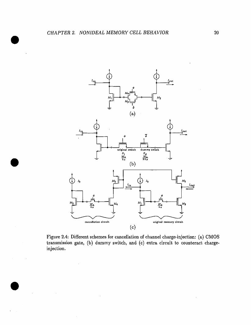
There are a lot of schemes proposed to compensate fol' charge-injedion errors.
Sorne common ones include a CMOS transmission gate as the switch and the so-called
"dummy switch" scheme [23, 3]. The dummy-switch scheme consists of the switch
transistor and another transistor with its drain and source terminaIs shorted togct;hel'.
Another more complicated scheme has also been recently proposed [24]. These tlll'ee
schemes are presented in Figure 2.4. In the work of this thesis, the dummy switch
approach was adopted. This was donc to keep the circuits as simple as possible and
to minimize silicon area. A comparison was made between the transmission gate
approach and the dummy switch scheme, but little difference was seen. The dummy
switch scheme is depicted with the memory cell in Figure 2.4(b). It is composed of
the original switch SI and an additional switch Sd. Since 8d is designed to be half
the size of SI and clocked by 4>, the charge injectcd by SI is hoped to be compensated
by an equal but opposite charge (to a first-order approximation) from the dummy
switch Sd.
• Cf-fAPTER 2. NONIDEAL MEMORY CELL BEHAVIOR 20
+---_---:'
• CHAPTER 2. NONIDEAL MEMORY CELL BEHAVIOR
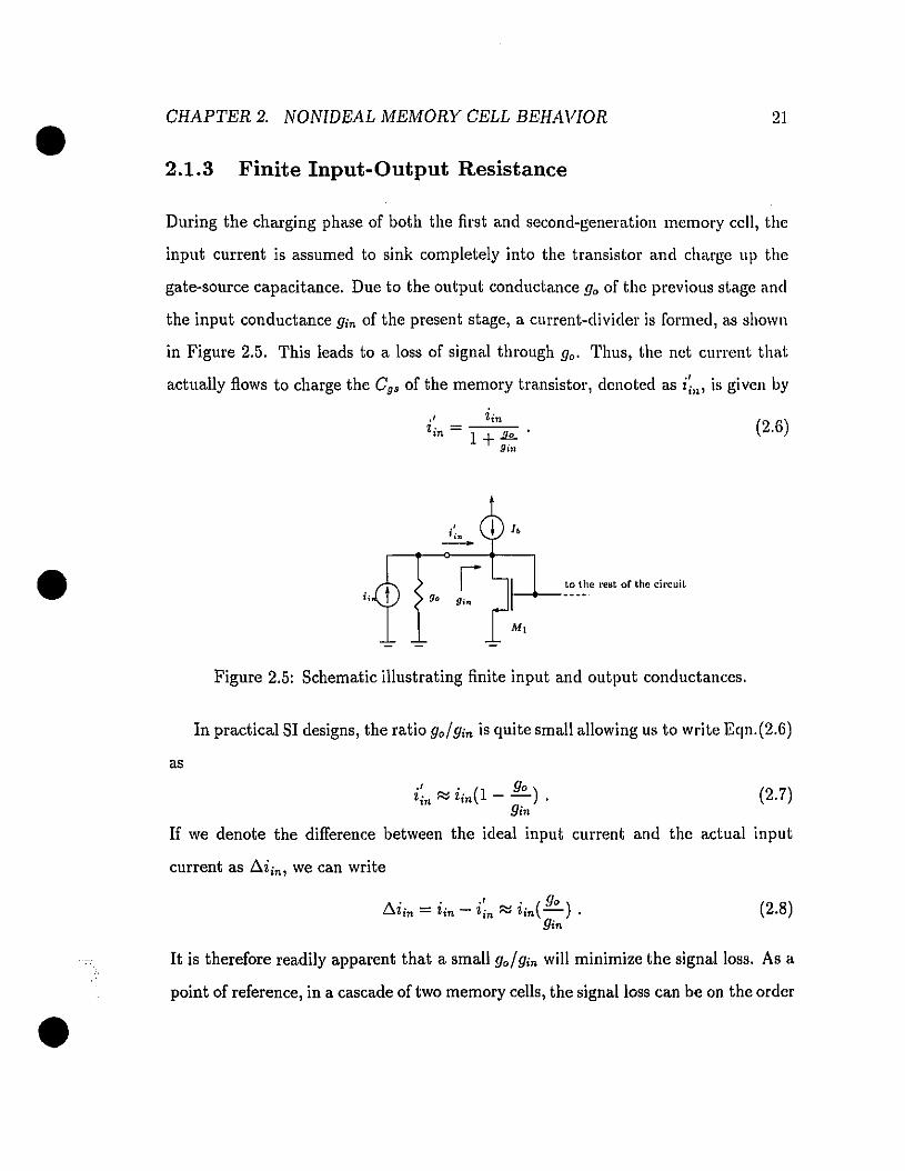
2.1.3 Finite Input-Output Resistance
21
During the charging phase of both the first and second-generation memory ccII, the
input current is assumed to sink completely into the transistor and charge up the
gate-source capacitance. Due to the output conductance go of the previous stage and
the input conductance gin of the present stage, a current-divider is formed, as shown
in Figure 2.5. This leads to a loss of signal through go. Thus, the net current that
actually flows to charge the Cgs of the memory transistor, denoted as i;", is given by
,1 'lin1 . = .,----"'-::
<Il 1 +.!J!l..Yin
(2.6)
• ii
.'lin-
go 9in
to the reüt or the circuit11-'-
Figure 2.5: Schematic illustrating fini te input and output conductances.
In praetical SI designs, the ratio go/gin is quite small allowing us to write Eqn.(2.6)
as
.' . (1 go )'lin:::::: 'lin - - .gin
(2.7)
If we denote the difference between the ideal input current and the aetua! input
current as tl.i in , we can write
A • • .' • (gO)UZin = 'lin - tin ~ 'lin - .
Yin(2.8)
•It is therefore readily apparent that a small go/gin will minimize the signal loss. As a
point of reference, in a cascade of two memory cells, the signalloss can be on the order

of 1%of the input curre,nt level. In most situation, this level of error is unacceptable.,
Thus to reduce the effed of loading, a lower 90/9in ratio is usually sought. This can be,
achieved by incorporatir\g cascoded transistors into the memory cell [25]. Among ail
• CHAPTER 2. NONI]j~EAL MEMORY CELL BEHAVIOR 22
•
•
1
the methods of cascoding published to date, the regulated-cascode memory cell [26]1
seems to he the best for SI Implementation. It has heen shown that a factor of 103 to
106 improvement in the 90/9in ratio is possible over the simple memory cells shown in
Figure 2.1(a) and 2.2(a). Besides, there are other added benefits when designing with
regulated cascode cells, such as improved capacitive isolation (more on this later).
2.2 Specifie Errors
After discussing the common sources of errors in SI circuits, we will dedicate this next
section for outlining errors that are specifie to either the first or the second-generation
memory cell. With the different switch arrangement in the two memory cells, it is
logical to expect them to encounter different causes of errors. Instead of going over
every possible source, we are going to highlight two major ones which has surfaced in
the open literature since the introduction of the SI techniques. Here, we denote them
as sensitivity to component mismatches and variation in input-impedance leve/.
2.2.1 Sensitivity To Component Mismatches
Owing to the mirroring action involved, the current gain in SI cells strongly de
pends on the matching of transistors. Any fabrication processing error willlead to an
inaccuracy in this gain. Thus, it is always desirable to have SI circuits that are insen
sitive to this component variation. According to Hughes et al in [11] they conclude
that the second-generation structure has a much hetter sensitivity behavior than that
of the first-generation structure. On taking another look at the sensitivity of the first
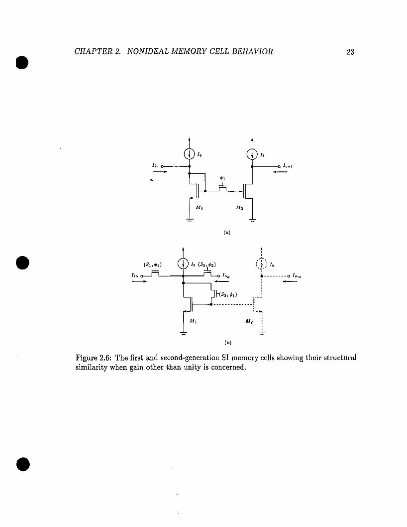
• CHAPTER 2. NONIDEAL MEMORY CELL BEHA\fIOR 23
1 J, 1 Jo
+----o1"UI-
-
(a)
!,,~:-~
: ~ ) /".-',.--------0/"'",,,,,,
,~_ .,J
"1--"---- -- -- -- ----l:.'"_ .,,,
M2 :,,.. -
f----,-•(b)
Figure 2.6: The first and second-generation SI memory cells showing their structuralsimilarity when gain other than unity is concerned.
•
• CHAPTER 2. NONIDEAL MEMORY CELL BEHAVIOR 24
•
•
and second-generation memory ceUs, we have discovered that this is true only if the
current gain of the memory transistor is unity. In such a case, the output current
can be derived directly from the memory transistor itself through JOd as shown in
Figure 2.6. Clearly then process variation in transistor M, will not alter the value
of current stored or retrieved from the ceU. This is an important advantage of this
type of memory ceU over al! other cel! types. In contrast, if the current gain is other
than unity, process variations will affect the output current, as it is derived through
a current mirror, regardless of it being implemented as a first or second-generation
memory cel!. In fact, since the retrieval of the output current iô exactly the same in
either case, they will have identical sensitivity behavior to component variations. In
most filter applications a current gain other unity is required, we therefore conclude
that the sensitivity problem to component mismatches has the same effect on both
the first or second-generation memory ceUs.
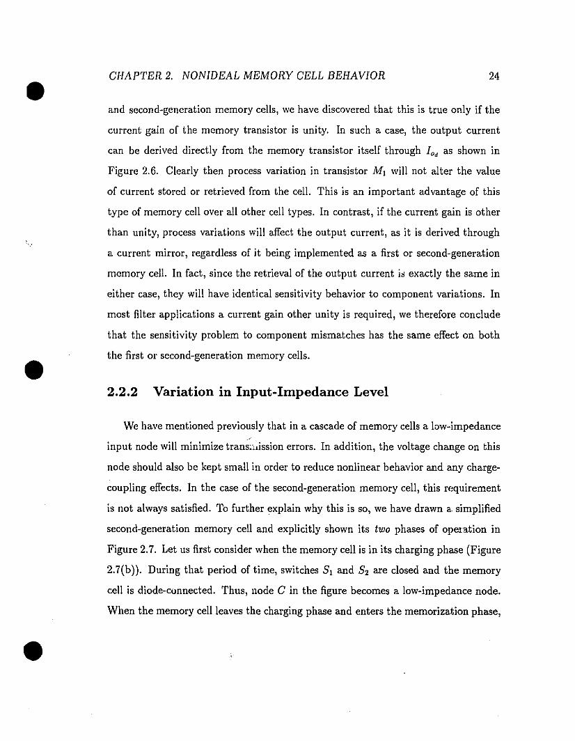
2.2.2 Variation in Input-Impedance Level
We have mentioned previously that in a cascade of memory ceUs a low-impedance
input node will minimize trans~,.ission errors. In addition, the voltage change on this
node should also be kept smaU in order to reduce nonlinear behavior and any charge
coupling effects. In the case of the second-generation memory ceU, this requirement
is not always satisfied. To further explain why this is so, we have drawn a. simplified
second-generation memory cel! and explicitly shown its two phases of operation in
Figure 2.7. Let us first consider when the memory ceU is in its charging phase (Figure
2.7(b)). During that period of time, switches S, and S2 are closed and the memory
eeU is diode-connected. Thus, uode C in the figure becomes a low-impedance node.
When the memory ceUleaves the charging phase and euters the memorization phase,
• CHAPTER 2. NONIDEAL MEMORY CEU BEHAVIOR 25
(a)
• ~'w.imp.2.node, C
(b)
5,
high.impeda.nce 1node, C ~ lb
0---<>-.-.,.....:::.;----<>
(c)
•
Figure 2.7: Describing the phenomenon of variation of input-impedance level: (a)second-generation SI memory œil with simplified switches, (b) during the chargingphase: SI and S2 are both ON, node C is low-impedancej (c) before the memorizationphase: S2 and S3 are opened when SI is still ON, node C changes to high-impedance.
• CHAPTER 2. NONIDEAL MEMORY CELL BEHAVIOR 26
•
•
82 opens and node C is transformed into a high-impedance node. Any current being
pushed into or pulled from this node will cause a sudden change in the node voltage.
Under ideal conditions SI and 82 will be opened at the same time and no current
will be forced into this high-impedance node. In practice, however, switches SI and
S2 are connected to the l'est of the circuit distinctively and operated under different
conditions. Thus, it is unreasonable to assume they will turn off at exactly the same
time. Consequently, a residual current will flow into the high-impedance node of the
memory cell as shown in Figure 2.7(c), resulting in a voltage spike at node C. This
current enters the node at the end of dock </>1 and leaves at the beginning of dock
</>2. Due to the changing circuit conditions, the rising and falling edges of this voltage
spike will differ from each other. Since the drain terminal of the memory transistor
directly experiences this changing voltage, a net charge is coupled through the drain
gate capacitance to its gate terminal, thus introducing large memorization error. In
fact, as wc shalilater shown in Chapter 3, these errors tend to dominate over ail other
errors mentioned so far.
2.3 Conclusion
This chapter has outlined the non-ideal behavior of the first and second-generation
memory cells. The errors created by such non-idealities has been categorized into
common err01'S and specifie errors. Common errors which are present in both the first
and second-generation memory cells indude the settling-time error, charge-injection
error and finite input-output conductance error. Specifie errors are those appear only
in one cell type. One of them - the sensitivity problem - which was once thought
to be specifie has been shown for the most part (i.e. when non-unity current gain
is concerned) as common to both memory cells. The other - variation in input-
• CHAPTER 2. NONIDEAL MEMORY CELL BEHAVIOR 27
•
•
impedance LeveL - is unique to the second-generation memory ceU and the error t;!ll1S
generated can be very significant. If great caution is not exercised, considerable levels
of signal distortion may arise during normal operation. It is, therefore, the author's
belief that structures comprised of the first-generation memory ceUs will out perform
structures designed with second-generation ceUs. In the next chapter, we will provide
an extensive study involving simulations of the first and second-generation cUITent
memory ceUs. The investigation is then broadened in 1ater chapters to cover other SI
building blocks, such as delay and integrator ceUs.
•
•
•
Chapter 3
Transient Analysis of SI MemoryCeUs
"The problem of the variation in the input-impedance level at the current-summing
node in the second-generation memory cell was addressed in the previous chapter. It is
argued that such a drawback will create unwanted glitches and memorization errors in
the output current signal. In this chapter we will provide evidence supporting such a
daim based on various transistor-Ievel HSPICE simulations. Apart from the transient
analysis we will also provide the Total Harmonie Distortion (THD) measure for the
first and second-generation memory ceUs as an indicator of their overalllinearity. On
account of the study, a novel dock scheme will be proposed to minimize this glitching
effect. In addition, we will also introduce a more complicated circuit structure to
replace the simple memory ceU arrangement for enhanced linearity performance.
3.1 SI Memory Cell
To begin our investigation of the transient behavior of the first and second-generation
SI memory ceUs, we performed a transistor-Ievel simulation using the HSPICE simu-
28
• CHAPTER 3. TRANSIENT ANALYSIS OF SI MEMORY CELLS 29
•
•
lator. The schematics of the actual circuits used for simulation pm'poses are shown in
Figure 3.1. The circuit specifications were chosen to correspond to actual SI circuits
as much as possible. In each case, the memory cell was clocked at a rate of 500 kHz
with a two-phase non-overlapping clocking scheme shown in Figure 3.2. The Clll'rent
biases (h) were idealized and set at a value of 20 pA. A 20 kHz sampled-and-held
input sinusoidal current signal with an amplitude (Jamp) of 10 pA was then fed into
the circuit, leading to a drain current modulation factor m (where m = Jamp/ h)
of 50%. Although an unsampIed sinusoidal signal can be applied to the input of a
first-generation memory cell due to its inherent track-and-hold property, a sampled
and-held input current was used for making a fair comparison between the two cells.
The memory transistors in both cells were modeled after a typical device found in a
1.2 pm CMOS process with identical aspect ratios of 400 pm/50 pm. In practice, this
would ensure equal kJ noise levels. An arbitrary gain of unity was assigned to bath
cells for the ease of data manipulation. Similarly, the switches were designed using the
dummy switch scheme discussed in Chapter 2 with an aspect ratio of 4 pm/1.2 pm for
the main switch and 2 pm/1.2 pm for the dummy switch. The dummy switch scheme
is only applied ta those switches which are capable of interfering with the memorized
charge on Cgs • In particular, for the circuits shown in Figure 3.1, the dummy switch
scheme is applied to 81 in the first-generation memory cell and 82 in the second
generation cell. Ali other switches were implemented with simple NMOS switches.
To retrieve the output currents, the output node of each circuit was connected to a
constant voltage source whose level was set at the quiescent drain-to-source voltage
of the output transistor. In the case of the first-generation memory cell, only one
output (Jout) is availablej while in the second-generation memory cell there is a choice
of direct or mirrored output (JOd or JOm )' In ail cases, the output current is defined
as the current f10wing into the drain of the output transistor.

• CHAPTER.J. TRANSIENT ANALYSIS OF SI MEMORY CELLS
,
1 l, 1 /0Jin [out
-~1'···
(5" .Il/51H or [.in
..L
M, M,
(al
30
•1 l,
c
1 /0
•
(b)
Figure 3.1: Schematics of SI memory cells for HSPICE simulation purpose: (a) firstgeneration and (b) second-generation. Notice the extra switch at the input of thesecond-generation memory cell is required to provide a signal path to ground.

• CHAPTER 3. TRANSIENT ANALYSIS OF SI ME1HORY CELLS 31
,plI S1
rP2' S3
______ .3witclION
_______ 3witch OFF'
•
•
Figure 3.2: Simple two-phase non-overlapping dock scheme used fol' the first andsecond-generation current memory cells.
3.1.1 First-Generation Memory Cell
On simulating the SI memory cell of Figure 3.1(a) with I-ISPICE, the transient
behavior of the output current signal was computed and is depicted in Figure 3.3(a)
with a solid line. The sampled-and-held input current is also shown and marked
with a dotted line. According to these two curves, the output signal appears to
be an inverted replica of the input waveform with a delay of half-a-dock pet·iod.
Figure 3.3(b) illustrates the output current behavior over one dock period. As is
evident, during the first half of the dock period (which was designated as ,pd, the
output current charges up to the input CUITent level in a monotonie mannel'. Fol' the
remaining duration of the dock period, the output current is held constant. This
behavior on both the charging and memorization phases, is consistent with that
predicted in Chapter 2. In particular, the charging phase will be dominated by a
single-time-constant settling behavior.
In order to compare the simulated result with our predicted one, we have listed
sorne data evaluated at the operating point of the first-generation memory cell using
I-ISPICE in Table 3.1.
• GHAPTER 3. TRANSIENT ANALYSIS OF SI MEMORY CELLS
lFX~10~"-'-_;:::;:::::!:;'-'--~-~-~=::!:;"-~1
32
§:ê ail
-0.5
-.~ input currenl
_ output current
(.................;
•
•
-1 L--,--~:;:=:::::c=---,----,-_--,----==::c~--..Ja 0.5 1.5 2 2.5 3 3.5 4 4.5 5
(a) x la"
5 ~ 'c? ..o~"9iog pM••.....<cI~.?mamo".aliQnp~ <,~§: ;ê4 ... ~
il .3 ..... ,..
lb)
Figure 3.3: Transient response of the first-generation SImemory cell. (a) A sampled-and-held output signal resembling the input signal inverted. (b) A c1ose-up viewof the output current during the charging phase.
Ist gen. 2nd gen.CgOt 0.920835 pF 0.920835 pFCg02 0.920835 pF 0.920835 pFCgl!J!ot 1.841670 pF 1.841670 pF9m, 8.50xIQ-sU 8.50xIQ-sU
Table 3.1: Operating Point Information for the first and second-generation SI memorycells.
Using the equation describing the time-constant (Tf;rot) of the first-generation
memory cell in Chapter 2, together with the data supplied in Table 3.1, we can solve
for Tf;ro. as follows:
• GHAPTER 3. TRANSIENT ANALYSIS OF SI MEMORY GELLS
1.842 pF~
8.50X10 5 U
= 21.59 ns
3·,~
•
•
Based on the simulated output response in Figure 3.3(b), the time-constant; was
found to be approximately 29.43 ns. This is a bit larger than that calculated by hand
analysis but within the same order of magnitude. The difference can be contributed
to two factors. First, Eqn.(2.4) used to calculate the time-constant was based on the
small-signal model of the MOS tra~sistor. In our case where the input current; reaches
as high as 50% of the bias current, the small-signal model may not be accurate enough
to predict the transistor behavior at the input current extrema. Second, the memory
transistor experiences a decreasing transconductance over the charging phase, thus
resulting in a slightly larger time-constant. For instance, at the start of the charging
phase, gm = 8.5xl0-5 U, however at the end of the charging phase gm = 7.39xl0-5 U.
One important attribute of the output current that is central to this thesis is the
slight step change that occurs at the end of the charging phase. Such a subtle step
change in current has important ramifications on the linear behavior of the memory
cell. This current deviation can be accounted for by:
i) the small amount of charge-injection induced by the dummy switch, and more
importantly,
ii) the channel-length modulation effect. Recall that the memorized current is es
tablished in transistor Ml (Figure 3.1) when its drain-source voltage equals its
gate-source voltage during the charging phase. In contrast, during the mem
orization phase, the output current is retrieved from transistor M2 with its
drain tied to a constant voltage source which may or may not be equal to the
gate-source voltage. This difference in drain-source voltage will then cause a
• CHAPTER 3. TRANSIENT ANALYSIS OF SI MEMORY CELLS 34
11:"ê 0êB
-0.5
-,- input currant
_ output current
6
g4"êê 2
B O'-_J-J'U
-20'-~0.~5--'--""'1."'5 -~.~--2=".5:-----O-3--3"".5""'----'-4--4"':.5--J5
(b) x 10"
•Figure 3.4: Simulated transient responses of the secondgeneration rnemory cell highlighting the glitching problem: (a) the mirrcredoutput [am' and (b) the direct output [ad'
variation in the output current.
3.1.2 Second·Generation Memory Cell
•
A similar simulation is performed for the second-generation memory cell in order
to compare the behavior of the two cells. The result of the transient analysis is shown
in Figure 3.4. Again, the input current is indicated by a dotted line while the output
cIment is represented by a solid line. In Figure 3.4(a), the mirrored output current
of the second-generation memory cell [am has a shape that is similar to that of the
output current of the first-generation cell. However, also noticeable are the glitches
that exist in the output waveform. The other output current (lad) taken directly
• OHAPTER 3. TRANSIENT ANALYSIS OF SI MEMORY OELLS 35
•
•
from the memory cell is shown in Figure 3.4(b). Unlike the output currents that we
have seen so far, I Od is only available during dock phase q,2. This is a consequence of
having a switch (switch Sa in Figure 3.1) connected in the output path. Moreover,
IOd also carries unwanted glitches at the transitions between dock q,l and <h.
Before accounting for the abnormal glitches in the output signais of the second
generation memory cell, let us first focus on its settling behavior. A portion of the
mirrored output waveform JOrn is enlarged in Figure 3.5(a) to highlight this behavior.
The intervals denoting the charging phase and the non-overlapping phase are super
imposed on the plot of the output signal. The non-overlapping phase corresponds
to the time when both dock phases q,l and q,2 are low, which in turn implies their
respective switches are OFF. During the charging phase, the output current follows
a monotonic charging behavior and should be characterized by time-constant '-socoud
which is approximately the same as '-Jirs. of the first-generation memory cell coun
terpart. Calculation based on the charge transfer process of Figure 3.4(a) shows that
'-second is around 25.4 ns. Again, the time-constant is slightly larger than that pre
dicted by the simple STC theory at 21.6 ns but the difference can be accounted for
by the varying transconductance of the memory cell.
Besides this phenomenon of varying transconductance, the output signal deviates
significantly from that of the first-generation cell by having a sudden dip in the current
level during the non-overlapping dock interval. This is evident by the glitches seen
in Figure 3.4. To understand such phenomenon, it is helpful to take a look at the
voltage (Va) at the current-summing node 0 at the input of the memory cell in Figure
3.1. This voltage level is depicted in Figure 3.5(b) over a dock period. As can be
seen, at the beginning of the non-overlapping phase, Va suddenly increases to a large
voltage (approximately 5V). This can be explained by the fact that node 0 is being
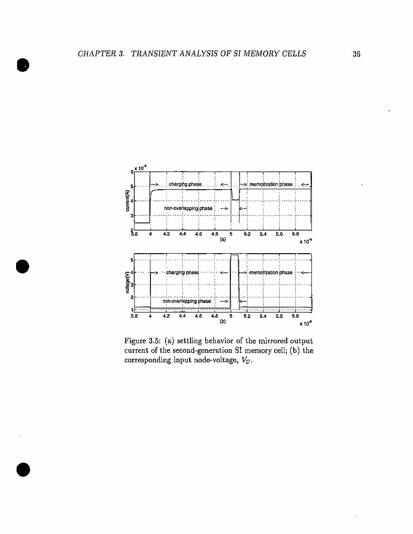
• CHAPTER 3. TRAN8lENT ANALY818 OF 81 MEMORY CELLS 36
5 ,-.~~ ..
§:ê4
il3 ....
f-,
§.e 4
. ······11-= , ..~on.ove~lapplngjphase --->
u « U U 5 U U U U(a) x 10·
• 5
2;4œ~3g
2
13.6
., .. ,. j"> .. , ~hargln~ phas~ ,., '<._. ..>~·memoflzatlon?haSe'j .'<•••
n~;;~~ërl~PPI~9' ~hase' "1" -->' ... , ,.
4 U « U U 5 U U U U(b) x10·
•
Figure 3.5: (a) settling behavior of the mirrored outputcurrent of the second-generation SI memory cell; (b) thecorresponding input node-voltage, Va.

• CHAPTER 3. TRANSIENT ANALYSIS OF SI iHEMORY CELLS 37
transformed into a high-impedance node. Since there is still small amount of residual
current going through the input switch to node C, a large voltage is establised on this
high-impedance node. When the memory cellleaves the non-overiapping phase and
enters the memorization phase, node C is changed back to a low-impedance node and
we see that Va then drops back down to a level quite close to that at the end of the
charging phase. With node C changing from low-impedance to high-ùnpcdance and
high-impedance to low-impedance, different amounts of charge are coupied thl'Ough to
the gate-source capacitance of the memory transistor thus creating a memorization
error. Such error varies with the input signal and leads to large levels of harmonic
distortion. This is a major drawback of the second generation SI strudures. ln
the next section, we will propose a novel clocking scheme for the second-generation
memory cell in the hope of minimizing such memorization error.
• 3.2 Reducing Glitches in SI Circuits
•
The memorization errer is a result of the variation of input-impedance level at the
current-summing node. To minimize such error, it is essential that no current is
pushed or pulled from the current-summing node when it varies From a low-irnpedance
to high-impedance state and vice versa. A simple method that can accomplish this
is to redirect the input residual current through a low-impedance path to ground.
This can be achieved by overiapping the falling edge of the clock conl;rolling switch
SI and the rising edge of the clock controlling switch 83 in the circuit of Figme 3.1.
Realizing that the output current can be sampied at the end of the clock controlling
switch 83 , this modification should have little effect on the final value of the ontput
current samples provided that the dutYcycle of the output clock phase is long enough
to allow for proper settling. Another step to enhance the performance of the memory

• CHAPTER 3. TRANSIENT ANALYSIS OF SI MEMORY CELLS 38
•
•
ccli is to force switch S2 to dose before switch SI does. This ensures that the memory
cell enters the charging phase before any input current is fed in. In summary, the
timing requirements on the three switches, Sb S2 and S3' are:
i) switch 82 should be turned ON and OFF before SI to ensure that a proper
input current is memorizedj
ii) S2 and 83 should be non-overlapping to avoid any current leakage through S3;
iii) SI and S3 should overlap during the non-overlapping period of S2 and 83. This
ensures a signal path to ground and avoids the high-impedance node.
With these new timing arrangements, a new 3-phase dock scheme is proposed to
operate the second-generation memory cell. This new scheme is depicted in Figure
3.6 and will be used in place of the 2-phase non-overlapping dock scheme originally
suggested.
~.. _______~witch ON
r,bI,SlY' :,1 i 1 1 r-Il
_______ s.witc/J OFF
,~ il 1 1r/J!,52
rP2,S3 Il '1 1 1 LFigure 3.6: Proposed modified 3-phase dock scheme to reduce glitching effect in thesecond-generation memory cell.
An HSPICE simulation was conducted with the new dock scheme incorporated
into the second-generation memory cell. The results of the transient analysis are
shown in Figure 3.7 with the mirrored output current at the top and the direct output
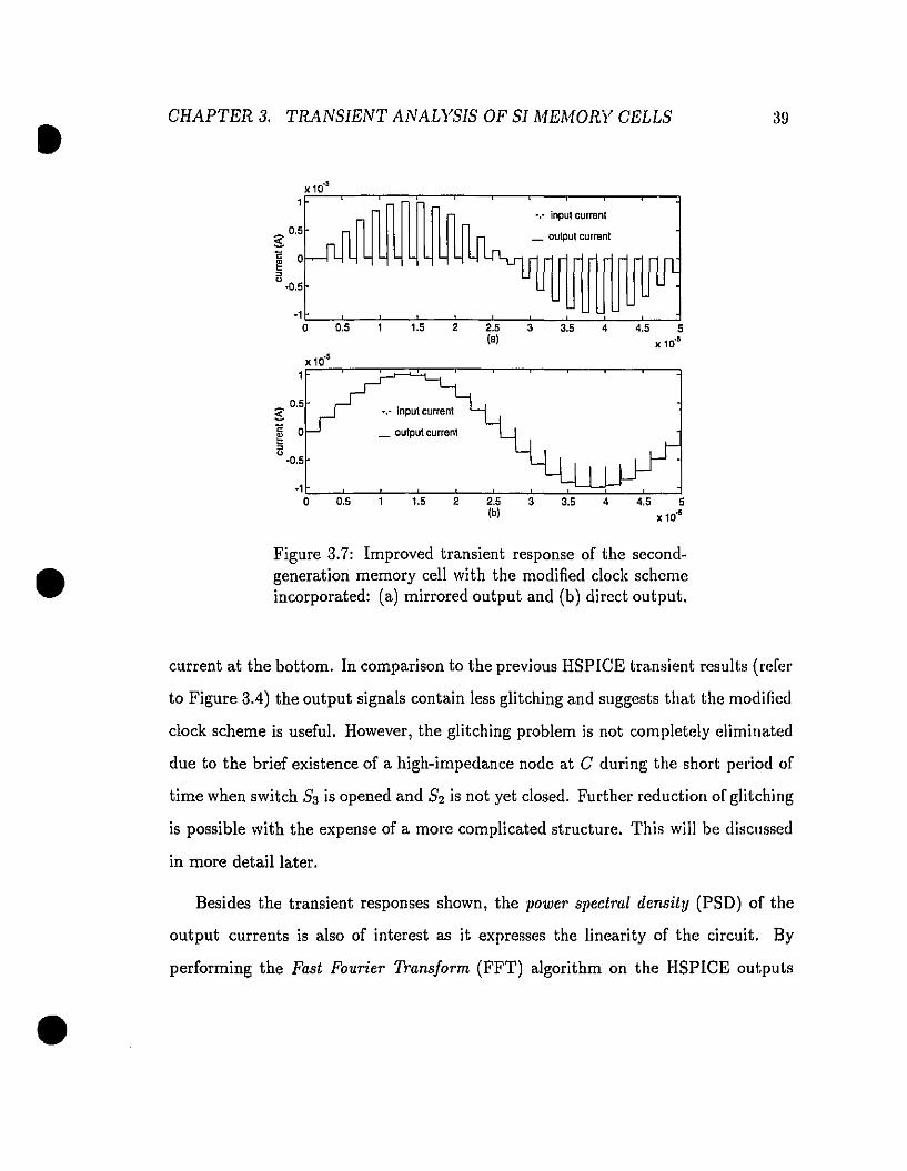
• CHAPTER 3. TRANSIENT ANALYSIS OF SI MEMORY CELL5 39
"," input current
_ output currantg 0.5
E 0êil
·0.5
•
•
·1 ~-=-=--:-_-=,=_-:-_::,::-_-=--::~:...::i_-:'::--~o 0.5 1.5 2 2.5 3 3.5 4 4.5 5(a) le 10.5
_ output curranl
.1!=---;;-;--:--7';--;;----;;';:,----:----;.,==~__:'::___=!o 0.5 1.5 2 2.5 3 3.5 4 4.5 5(b) x 10"
Figure 3.7: Improved transient response of the secondgeneration memory cell with the modified dock schemeincorporated: (a) mirrored output and (b) direct output.
current at the bottom. In comparison to the previous HSPICE transient rcsults (refer
to Figure 3.4) the output signais contain less glitching and suggests that the modified
dock scheme is useful. However, the glitching problem is not completely e1iminated
due to the brief existence of a high-impedance node at C during the short period of
time when switch 53 is opened and 52 is not yet dosed. Further reduction of glitching
is possible with the expense of a more complicated structure. This will be discussed
in more detail later.
Besides the transient responses shown, the power spectral density (PSD) of the
output currents is also of interest as it expresses the linearity of the circuit. By
performing the Fast Fourier Transform (FFT) algorithm on the HSPICE outputs

• CHAPTER 3. TRANSIENT ANALYSlS OF SI MEMORY CELLS 40
•
•
[27], the corresponding PSD data can be obtained. In Table 3.2, the PSD data
expressed in dB is displayed in terms of the rel<ttive output tone power to the input
tone power. Measures for both the first and second-generation memory cells are given.
Harmonie First- 2nd gen. (modified dock) 2nd gen. (simple dock)Tone Generation direct mirrored direct mirroredDC -47.03dB -44.35dB -48.46dB -35.54dB -37.91dBprincipal -0.038dB -0.095dB -0.053dB -0.247dB -0.206dBsecond -61.42dB -53.69dB -60.73dB -33.38dB -33.79dBthird -77.97dB -75.98dB -77.12dB -39.97dB -39.89dBfourth -80.97dB -89.26dB -89.12dB -40.68dB -40.63dBTI-ID 0.0873% 0.210% 0.0936% 3.552% 3.488%
Table 3.2: Power Spectral Density data of simple first and second-generation SI memory cells.
Also enumerated is the measure of the total harmonie distortion (THD) generated
at the output. This measure is defined as the square-root of the ratio of the total
power in the harmonie tones of the output signal to the power of the fundamental
output tone, Le.,t
THD~ (I:~~~llio~nll~)2 (3.1)Il zoUltlb
Here Il.1l~ denotes the L 2 norm operator of the power and the signal iouln represents
the nt" harmonie tone of the output spectrum. It is evident from Table 3.2 the
first-generation memory cell has less loss at the principle tone frequency, less DC
offset and smaller THD than the second-generation memory cell, with or without
the modified clock. If the 2-phase non-overlapping clock scheme is used with the
second-generation cell, the THD was seen to rise as high as 3% and we conclude that
this type of design is NOT recommended for linear applications. In comparison with
other designs intended for linear applications, it is common practice to expect at
most a 0.1% of THD. If this rule of thumb is imposed on the memory cells under test,
• CHAPTER 3. TRANSIENT ANALYSIS OF SI MElIWRY CELLS
1 l,
1 "D
1d'J - 6,fd,J 1 1D
1"
~ldl-M, + Ild, ~VaS2 SX
y + M,
Vasi SMo
S
41
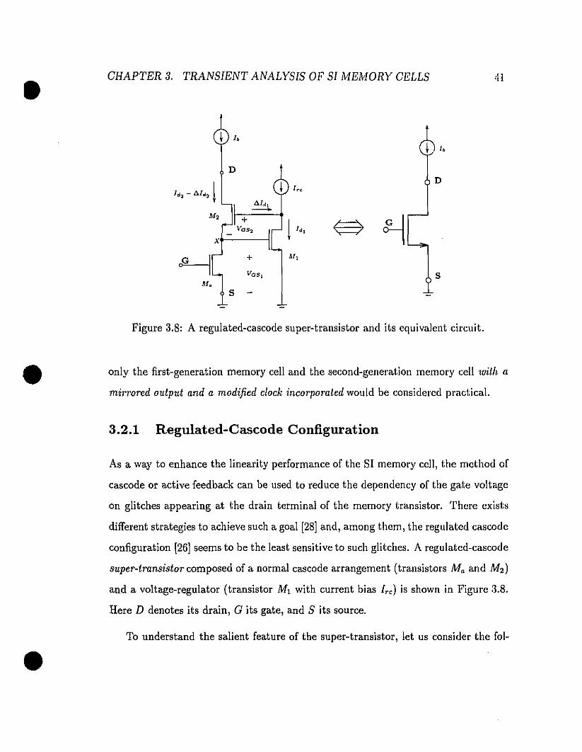
•
•
Figure 3.8: A regulated-cascode super-transistor and its equivalent circuit.
only the first-generation memory cell and the second-generation memory cell will! li
mirrored output and a modified dock incorporated would he considered practical.
3.2.1 Regulated-Cascode Configuration
As a way to enhance the linearity performance of the SI memory cell, the method of
cascode or active feedhack can he used to reduce the dependency of the gate voltage
on glitches appearing at the drain terminal of the memory transistor. There exists
different strategies to achieve such a goal [28] and, among them, the regulated cascode
configuration [26] seems to he the least sensitive to such glitches. A regulated-cascode
super-transistorcomposed of a normal cascode arrangement (transistors Ma and M2 )
and a voltage-regulator (transistor Ml with current bias Ire) is shown in Figure 3.8.
Here D denotes its drain, Gits gate, and S its source.
'1'0 understand the salient feature of the super-transistor, let us consider the fol-

• CHAPTER 3. TRANSIENT ANALYSIS OF SI MEMORY CELLS 42
(3.2)
•
•
lowing situation: when there is an sudden increase in the voltage at node D, say b.VD,
the gate-source voltage of transistor Ml (Vos,) will rise correspondingly. This change
in Vos, in turn increases the drain current of Ml (Id, + b.ld,). Since transistor Ml
is biased by current source Ire, the excessive drain current required (b.ld,) is forced
to come from the gate of transistor M2, thus discharging its gate-source capacitance
and reducing its gate-source voltage (Vos,). A corresponding decrease in the drain
current of transistor M2 (Id,) then occurs. As a result, the current going into the
memory transistor Ma is lessened and Vos, is reduced, repelling the original increase
of Vos, due to b.VD.
According to a detailed small-signal analysis, the change in Vos, with respect to
a change in VD can be quantified by
b.Vos, [2 2]-1b.VD = gmrds ,
where gm and rds are correspondingly the transconduetance and the output resistance
of the equal-sized transistors, Ml and M2. The ratio of gate-source voltage to the vari
ation of output voltage shown in Eqn.(3.2), i.e., b.Vos.!b.VD, is gmrds times smaller
than that of the normal cascode arrangement. In other words, the regulated-cascode
configuration is gmrds times less sensitive to output voltage variation than conven
tional cascode arrangement. In faet, this increase in robustness to output voltage
variation allows the memory transistor to be operated in triode without sacrificing
much accuracy [26].
In Figure 3.9, we have depicted the first and second-generation memory cells with
the regulated-cascode configuration incorporated. Similar HSPICE simulations as
cal'ried out on the simple memory cells were performed on the various regulated
cascode memory cells to investigate their transient and linear behavior. Results show
that the enhanced second-generation memory cell with a 2-phase non-overlapping
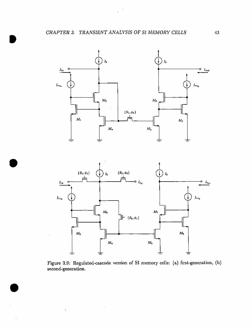
• CHAPTER 3. TRANSIENT ANALYSIS OF SI fvlEMORY CELLS 43
•
JOUI-
+-------0 Jo",-
Ms
M,
•Figure 3.9: Regulated-cascode version of SI memory cells: (a) first-generation, (b)second-generation.

• CHAPTER 3. TRANSIENT ANALYSIS OF SI MEMORY CELLS 44
•
•
scheme still bears high levcls of THD and is considered to be impractical for lin
car applications. Other results of the first-generation memory cell and the second
generation ccll with the 3-phase dock scheme are shown in Table 3.3 and Figure 3.10,
respectively.
Harmonic First- 2nd gen. (modified dock)Tone Generation direct mirroredDe -41.38dB -41.10dB -41.10dBprincipal -0.0098dB -0.0065dB -0.0065dBsecond -77.97dB -71.12dB -71.11dBthird -79.20dB -81.11dB -81.10dBfourth -80.69dB -85.53dB -85.52dBTHD 0.0215% 0.0298% 0.0298%
Table 3.3: Power Spectral Density of regulated-cascode SI memory cells.
At a first glance at Figure 3.10, the output waveforms of the various regulated
cascode memory cells appear to contain similar level of glitching as the simple memory
ccll arrangement seen previously in Figure 3.7. However, when their THD measures
are calculated, as listed in Table 3.3, the improvement is self-evident. Significant
reduction, dropping to as low as 0.03%, in the THD measures of both direct and mir
rored outputs of the second-generation memory cell is found. The same enhancement
is also noticeable in the case of the first-generation memory cell, which demonstrates
a superb THD of 0.02%. Summarizing what we have seen thus far, the regulated
cascode configuration has significantly improved the performance of the SI memory
cell.
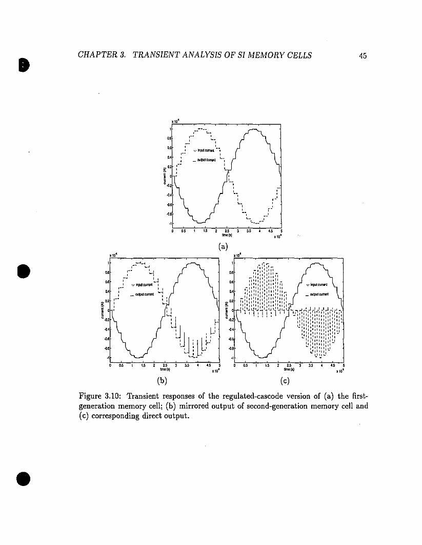
• CHAPTER 3. TRANSIENT ANALYSIS OF SI ll'IEMORY CELLS 45
4,5 5110"
ooo
011r-
I __1
.- 01__._.--
'5lm8!!)
c_o
1.5
o1
',' I1pu1cU1l1llll -j1
_ outpu1cullWll 1...,1
0-
,-,--1
0.5
0.8
O., 00,--
O, 00
-"•
.,•.8
(a).10"
• 0.8.. 11
0--.. 00
-" 0--1• 1
~ 0,i .,
••••.8
.,., ..
.....1_..1(- ... .1
:-~ ~11 0
""••• il~currenl 1o 1
_ oolp.JlcumJ1t '-io 1•
.10"
0.8..O.,
•.8
•.8
.,4.5 5
.10"0.5 '.5
(h) (c)
Figure 3.10: Transient responses of the regulated-cascode version of (a) the firstgeneration memory cell; (h) mirrored output of second-generation memory cell and(c) corresponding direct output.
•

• CHAPTER 3. TRANSIENT ANALYSIS OF SI MEMORY CELLS
3.3 Conclusion
46
•
•
Upte this point, the first and second-generation SI memory cells were compared exten
sively in terms of their transient behavior and linearity. The first-generation memory
cell was found to out-perform the second-generation counterpart by having a less dis
torted and more linear response. Although the performance of the second-generation
memory cell can be enhanced by the modified clock scheme and the regulated-cascode
configuration, the first-generation memory cell is still the recommended choice for lin
ear applications.
The memory cell is undeniably the basic element in the SI recipe and the infor
mation obtained thus far will help designers select the correct SI structure suitable
for their circuit implementation. Nevertheless, using SI memory cells alone, say for
example, as an analog memory unit is rare; rather they are used to form other build
ing blocks such as delay cells and integrators. It is therefore the author's intentions
in the next chapter to investigate the transient and linear behavior of such building
blocl{S and see whether similar conclusions result .
•
•
•
Chapter 4
SI Filter Building Blocks
The first-generation memory cell was shown in the previous chapter to exhibit better
transient behavior and linearity than the second-generation memory cell. This fad;
remains regardless of whether the modified dock scheme or regulated-cascode circuit
arrangement is used or not. In this chapter, the above argument will be furt;her
reinforced by broadening the analysis to other building blocks of the SI family. In
particular, two versatile SI building blocks will be considered, namely the de/av cell
and the integratoT. The delay cell is the generic filter building block in Finite Impulse
Response (FIR) filters and the integrator is the corresponding block used to form
Infinite Impulse Response (UR) filters.
4.1 SI Delay Cell
It was shown in the first chapter that the memory cell provides a delay of half-a-dock
period between the input and output current signais. By cascading two such cells, an
SI building block with delay of a full-dock period is achieved. Such a block is known
as a delay cell and has an important signal processing application.
47

CHAPTER 4. SI FILTER BUILDING BLOCKS
4.1.1 Operation of SI Delay Cells
48
-
lb)
Figure 4.1: SI delay cell formed by cascading two memory cells: (a) first-generationand, (b) second-generation.
A first-generation SI delay cell formed by connecting the output node of one
memory cell to the input node of another memory cell is shown in Figure 4.1(a). The
input CUITent is fed into the first diode-connected transistor Ma and the output signal
can be retrieved from the drain of transistor Md in the cascade chain. Signal gain can
be achieved by varying the ratio of the dimensions of transistor Mb to Ma or that of
Md to Mc. For instance, if we denote the aspect ratios of transistor Md as Ad and the
equal-sized transistors Ma to Mc as A, we can relate the input and output signaIs of
CHAPTER 4. SI FILTER BUILDING BLOCKS
the delay ceU according to
or, alternatively, in the Z-domain by
49
(4.1 )
('1.2)
The second-generation SI delay ceU is created in a similar way to the first-generation
delay ceU described above and is depicted in Figure 4.1(b). Between nodes A and B,
only one switch is shown as it is equivalent as having two switches controlled by the
same dock phase in series. As it was for the second-generation memory ccli, the delay
ceU has two types of output: a direct output IOd and a mirrored output 10"" Recall
that when signal gain of unity is required, the direct output is usedj othcrwisc, the
mirrored output has to be employed. Also rccaU that thc second-generation memory
ceU suffers large levels of glitching which is slightly improved by the modified dock
scheme (Figure 3.6). One would therefore expect a similar problem with the dclay
ceUs. Simulation reveals that this is indeed the case. Moreovcr, the modified dock
scheme proposed previously can not be used to reduce the levcl of glitching present
as no low-impedance path can be made to exist to re-direct any residual CUl'rent. At
this point in time, no solution seems to exist to remedy the situation, thus rendering
the second-generation delay cell as useless. Computer simulation will confirm this in
the next subsection.
4.1.2 Simulation of SI Delay Cells
HSPICE simulations are carried out on the first and second-generation delay cells.
Typical transistor models are used and current sources are idealized. Dummy switch

CHAPTER 4. SI FILTER BUILDING BLaCKS
o.a-,- Input currant
o.a_ output current
0.4
_ 0.25-ii 0 1
5 iu -0.2 \_.
-0.4
-o.a
·o.a
·1
1
'.
50
o 0.5 1.5 2 2.5 3tlme (sec)
3.5 4 4.5 5x 10.5
tFigure 4.2: Time-domain transient responses of the firstgeneration delay cell with and without the regulatedcascode configuration. Identical responses in each case.
schemes are applied to switches which are critical to the charge memorization oper
ation, otherwise minimum-sized MaS switches are used. The gain is set to unity for
both delay cells with ail the transistors being equally-sized with an width-to-length
aspect ratio of 400 p,m/60 p,m. A two-phase non-overlapping dock scheme at 500 kHz
is used to govern their operation. The input current has an amplitude of 10 p,A which
is half that of the bias cUITent, leading to a modulation factor of 50%. The frequency
of the input signal is 20 kHz, which is weil below the Nyquist rate. Retrieval of the
output current is performed by coniIecting at the output terminal of the delay cell to
a constant voltage source set to the nominal bias voltage of the output transistor.

CHAPTER 4. SI FILTER BUILDING BLaCKS 51
,
First-Generation Delay Cell: Results from the simulations performed with the
simple and regulated-cascode first-generation delay cell show little difference and arc
displayed as one plot in Figure 4.2. The input current is marked by dash-dottcd
line while the output current is indicated by a solid line. Apart from the initia.l
period when the delay cell is not yet settled, the output CUITent demonstrates a dose
resemblance to the input current with a full-dock period delay. By performing an FFT
analysis on the output signaIs, we have extracted the distortion levels and listed them
in Table 4.1. On scanning the list, we see that the principal tone of the regulated
cascode delay cell has less loss than that of the simple cell, approximately 0.1 dB
less attenuation. Also, less DC offset and smaller harmonic tones are generated by
the regulated-cascode configuration Collectively, the THD measure of the regulated
cascode implementation is 0.0496%, about one-third that of the simple delay cell
implementation.
Harmonic simple regulated cascodeTone configuration configurationDC -39.lOdB -53.11dBprincipal -0.139dB -0.026dBsecond -56.29dB -93.41dBthird -70.29dB -69.lOdBfourth -83.60dB -85.90dBTHD 0.1627% 0.0496%
Table 4.1: PSD measurement of first-generation SI delay cells.
Second-Generation Delay Cell: The transient behavior of the second-generation
SI delay cell,has also been simulated and the results are displayed in Figures 4.3 and
4.4 for the two different cell configurations (i.e. simple versus regulated-cascode). In
Figure 4.3(80), the direct output signal obtained from the simple cell is accompanied

CHAPTER 4. SI FILTER BUILDING BLOCKS 52
ali: 10"
'." input currenl
_ oulptJl currenl
g"2@ 1
a 111
0 ~- fi ,1 -Il - - - Il Il'... -III '1" 11 f.. 11 11)1
1 1 1 - /- 1 \
1 1 1 1·2 ' 1 1
1 1 11 1
"0 O.S 1.S 2 as 3 3.S 4 4.S Slime (sec) li: 10.5
(a)li: 10-5
t ,l ,
1
0.8 :1
0.6 1,,o.• 1
1
g0.21,,
~ 01 _
1
a~.1,
~..~..~...,
0 O.S 2 2S 3 35 4 4.S Slime (sec) le 10-5
(b)
Figure 4.3: Transient response of the second-generation simple SI delay cell from: (a)direct output, and (b) mirrored output.

CHAPTER 4. SI FILTER BUILDING BLOCKS 53
•
by huge amount of glitches, resembling the case of the simple memory cell with a 2
phase non-overlapping dock scheme describeà in the previous chapter. The amount
of glitching is significantly smaller when the output is taken through the mirrored
output, as shown in Figure 4.3(b). This is probably duc to the fact that the draiu
terminal of the memorization transistor is more isolated from the mirrored output
than the direct output. The PSD measurement on this ccli for both the direct and
mirrored outputs are listed in the first two columns of Table 4.2. As is evident in
both columns, the principal tone experiences huge loss (i.e. -0.332 dB and -0.414 dB)
and the THD for each cell is unacceptably high.
Repeating the same experiment but with the regulated-cascode configuration, the
transient response corresponding to each output is shown in Figure 4.4. Here wc
see less glitching is present in each case; nevertheless, sorne remains. The l'SD for
selected tones are taùulated in the two rightmost columns of Table 4.2. In short,
no significant improvement is evident in their levels, as the THD remains intolerably
high.
Harmonie simple configuration regulated cascodeTone mirrored direct mirrored directDe -27.60dB -26.82dB -25.62dB -25.60dBprincipal -0.332dB -0.414dB -0.170dB -0.170dBsecond -31.87dB -32.11dB -49.24dB -49.24dBthird -25.03dB -25.09dB -34.31dB -34.31dBfourth -32.70dB -32.68dB -33.83dB -33.83dBTHD 8.696% 8.712% 5.061% 5.062%
Table 4.2: PSD measurement of second-generation SI delay cells.
To condude this section, due to the high distortion level associated with the
second-generation delay cell, it is recommended that such delay cells should not be
used in SI circuits intended for linear applications.

CHAPTER 4. SI FILTER BUILDING BLOCKS 54
"," oulpUl currenl
_ input cunent
"," output corrent
_ input currenl
t
,".4
,".6
,".6
o
o.,
0.6
0.4
·0.6
'".,.,o
0.5
0.5
1.5
1.5
2 2.5 3lime (sec)
(a)
2 2.5 3lime (sec)
(h)
3.5
3.5
4
4
•
Figure 4.4: Transient response of the second-generation regulated-cascode SI delaycell from: (a) direct output, and (h) mirrored output.

CHAPTER 4. SI FILTER BUILDING BLOCKS 55
4.2 SI Integrator
Another important filter building block is the integrator. In this section. the SI
integrator in its two forms (first-generation and second-generation) will be studied
and comparisons will be made.
4.2.1 First-Generation
+-__0 1",,,,,.
Figure 4.5: First-Generation SI Integrator.
•
The first-generation SI integrator is shown in Figure 4.5. Transistors Ml to M'I
form a delay cell of unity gain. Its role is to duplicate the input current and delay
it by one dock period. This delayed current is then fed back to the input current
summing node. Transistors Mal and Mo, are added to mirror and scale the output
currents according to their width-to-length aspect ratios, AOI and Ao,. respectively.
Analysis of the circuit of the first-generation SI integrator revealed the following

CHAPTER 4. SI FILTER BUILDING BLOCKS 56
equations which govern the operation of the cell. Assuming that transistors Ml to
M4 to be unit-sized, we have
Ioio.(n) - Ioio.(n -1) = -Ao,Iin(n - 1)
Ioooo(n) - Ioooo(n -1) = Ao,I;n(n) .
(4.3)
(4.4)
By taking the z-transform of the above equations, the transfer function of the inverting
integrator is given by
t
Ioio• () _-_A....:o-,-,Z_-,....l-- Z =lin 1 - r l
and for the non-inverting output,
4.2.2 Second-Generation
(4.5)
(4.6)
•
The corresponding second-generation SI integrator is shown in Figure 4.6. A
pair of unit-sized transistors, Ml and M2 , are connected back-to-back to form the
integrator. Feedback action is inherent at the drain of these transistors and, as
such, we see no branch providing the feedback current If as in the case of the first
generation equivalent. Mirroring actions are provided by transistors MOI and Mo,
whose aspect ratios are Ao, and Ao" respectively. With sorne simple analysis, the
transfer functions of the two output signais with respect to the input current can be
shown to be equivalent to the expressions given in Eqns. (4.5) and (4.6).
4.2.3 Simulation Results
Having introduced the SI integrator, we should now be in a position to study their
transient response. However, before jumping right into the simulation, the author

CHAPTER 4. SI FILTER BUILDING BLOCKS 57
(S•• ;") -I~
"" (S,.;"I -1
1 2h
Figure 4.6: Second-Generation SI Integrator.
would like to stress that an integrator is seldom used alone without any feedback.
Feedback, which is pl'Ovided either globally 01' locally (i.e., damping), is necessary to
ensure DC stability. It was therefore decided to carry out the HSPICE simulations
with damped SI integrators to ensure stable operation.
Damping of an SI integrator (both first and second-generation) can easily be
achieved by inserting an additional feedback path from the inverting-end back to the
input node as depicted by the thickened line in the two circuits of Figure 4.7. Undcr
this condition, the two transfer functions of a damped integrator can be shown to be
•and
(4.7)
(4.8)

CHAPTER 4. SI FILTER BUILDING BLaCKS 58
1in.~+--1
+---0 lOin"
(al
(05". ,.,~) :
-l~~ (S~I":I+J
t---<o 10non--
•Figure 4.7: SI Damped Integrators formed by an additional feedback loop: (a) firstgeneration and (b) second-generation.
• CHAPTER 4. SI FILTER BUILDING BLOCKS 59
Here Ad symbolizes the aspect ratio of transistor Md which provides the necessary
level of damping. The other terms have the same meaning given previously.
To begin the study of the SI damped integrators, some I-ISPICE simulations were
conducted on the first and second-generation cells of Figure 4.7. The transistors
were arbitrarily chosen to be equal size and, as such, the inverting and non-inverting
transfer functions will become
and
=lTinv(z) = 1 _ L-I
2
(4.9)
(4.10)
•
•
Other simulation conditions including the input and bias CUITent levels, clocking
frequency and dummy switch schemes arc made the same as those used in the simula
tion of the SI delay cells (see Subsection 4.1.2). The only difference in the setup from
that given previously occurs with the clock scheme being employed. In order to avoid
the effect of input-impedance level variation in the second-generation SI integrator,
a new 4-phase clock scheme was found necessary. Before listing the transient and
linearity measurement, wc will side-track the reader and explain the design of this
4-phase clock scheme.
Design of 4-phase Clock Scheme: Referring to Figure 4.7(b), the following con
straints are imposed on the switches in the second-generation damped integrator.
Similar arguments apply to an undamped integrator.
Criterion 1: switch 84 is added to provide a signal path to ground for the input currcnt
coming from the source or a previous stage.

• CHAPTER 4. SI FILTER BUILDING BLOCKS 60
s,-_ ... ~--_+--o-l5----.,, '.~s,,"
SJ
(e)
(a) (h)
h' -LSI-----r- S-----r- , ,, - , -, '. , '.0 tS,(s,
S, S,, ,
• " "
(c)
-L••••• r- s, - , ,, '.0(\ s,,
"
Figure 4.8: Switching sequence of the controlling dock in the second-generationdamped integrator.
•

• CHAPTER 4. SI FILTER BUILDING BLaCKS 61
•
•
Criterion 2: switch 83 has to be turned ON and OFF before switch 81 to form a low
impedance node at A and to ensure a proper input CUl'1'ent is memorîzed;
Criterion 3: switches 82 and 83 should be non-overlapping to avoid charge sharing between
transistors Mt and M2 ;
Criterion 4: switch 82 is turned ON at the moment switch 83 is turned OFF to maintain
node A in the low-impedance state; and
Criterion 5: switch 84 has to be non-overlapping with 81 in order to prevent node A being
pu11ed to the analog ground.
The switching sequence is described pictoria11y in Figure 4.8 and the resulting 4
phase dock scheme is shown in Figure 4.9. With the novel dock scheme incorporated,
node A will become high-impedance for a short duration at the end of phase </12 when
a11 switches are opened (Figure 4.8(e)). Providentia11y, the residual current that may
be pumped into node A during this period of time is negligible. The only drawback
of this dock scheme is, perhaps, the shortening of the charging time available fol'
transistor M 2 • A similar dock scheme has recently been proposed by de Queiroz cl
al [29]. The scheme being presented here was developed independent of their worle
The results of the HBPICE transient analysis of the first-generation damped ill
tegrators (with simple and regulated-cascode configuration) and their corresponding
power spectral densities are illustrated in Figure 4.10 and Table 4.3, respectively.
Bince the output current waveforms for the simple and regulated-cascode structures
are very similar, only the latter transient waveforms are shown in Figure 4.10.

CHAPTER 4. 81 FILTER BUILDING BLOCK8•(S,.~! 1 1l r
........ .witch ON
........ n .. itc:h OFF
il(SI'~i)
i I! i1 1
(s,.~i ~ 1 l(5<1.4>;) 1 \ 1 l
62
•
•
Figure 4.9: A 4-phase dock scheme proposed for the second-generation SI integrator.
Harmonie simple configuration regulated cascodeTone inverting non-inv inverting non-invDe -40.87dB -47.99dB -67.33dB -69.96dBprincipal -0.766dB -0.682dB -0.510dB -0.512dBsecond -59.10dB -64.30dB -104.9dB -110.7dBthird -80.08dB -84.13dB -93.86dB -99.86dBfourth -108.6dB -l11.1dB -109.6dB -115.8dBTHD 0.1217% 0.0663% 0.00228% 0.00115%
'l'able 4.3: PSD data of the first-generation SI damped integrators.
The output signaIs of the inverting and non-inverting integrators, displayed in
Figure 4.10(a) and (b), respectively, demonstrate dean staircase waveforms. The
curve traces were plotted for a period of the input signal, starting from 50/Ls, when
the output currents are settled. In Table 4.3, the harmonie tones and THD values
are listed. It is obvious from this table that the first-generation SI damped integrator
gives reasonably linear behavior (see last row in Table 4.3. With the regulated-cascode
configuration incorporated, its low THD value illustrates the capability of this cell
fol' accurate signal processing. It may be argued that the results are masked by
the high-frequency roll-off of the transfer function of the damped integrator, thereby
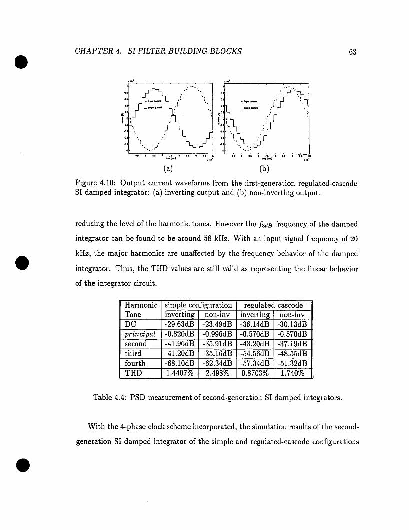
• CHAPTER 4. SI FILTER BUILDING BLaCKS 63
_._ ................-
iI.lllU .... flIO-1-) "0'
.,0'
......".,
.........,.' ,
".'
",,;,
"L-;,--..,',.:".:,,'',.....,.__--:---rr--.-~" 1 il 1 il 1 Il • '5 '0
_(Mcl .,0'
".. ,"
41 i"
·lJI •
(a) (b)
Figure 4.10: Output carrent waveforms from the first-generation regulated-cascodeSI damped integrator: (a) inverting output and (b) non-inverting output.
•reducing the level of the harmonie tones. However the hdB frequency of the damped
integrator can be found to be around 58 kHz. With an input signal frequency of 20
kHz, the major harmonies are unaffected by the frequency behavior of the damped
integrator. Thus, the THD values are still valid as representing the linear behavior
of the integrator circuit.
Harmonie simple configuration regulated cascodeTone inverting non-inv inverting non-invDe -29.63dB -23.49dB -36.14dB -30.13dBprincipal -0.820dB -0.996dB -0.570dB -0.570dBsecond -41.96dB -35.91dB -43.20dB -37.19dBthird -41.20dB -35.16dB -54.56dB -48.55dBfourth -68.10dB -62.34dB -57.34dB -51.32dBTHD 1.4407% 2.498% 0.8703% 1.740%
Table 4.4: PSD measurement of second-generation SI damped integrators,
•With the 4-phase clock scheme incorporated, the simulation results of the second
generation SI damped integrator of the simple and regulated-cascode configurations
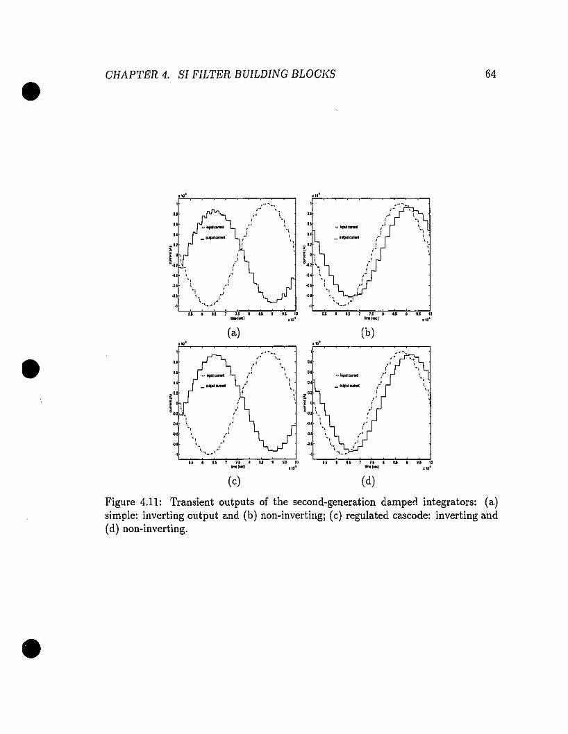
• CI-lAPTER 4. .'lI FILTER BUILDING BLOCK.'l 64
.,0' "0'
: .. ~.
.', ".. , ....-" .,, " _.....- ," ", ,, ,
" "" ,•.. , .,"" ..'.. , .., ,
., "._.~'.. • .. , " • u • u " " • u ," • u • " "lino!ooe) •,0' \l'no 1.... 110'
(a) (h).10' .,0'
,"".'".. .• " ", ","
" ", " ",IvJ_" ,
" , " _o~_ i
" ".,, gaJ ," 10,
, -0.2 !,,.. "", ,.• i ..
", ..' "\.,...-,,
u • u ," • u • u " " • "
, ,. • u • " "~"" ,'0" linolMCI .,0'
(c) (d)
Figure 4.11: Transient outputs of the second-generation damped integrators: (a)simple: inverting output and (b) non-invel'tingj (c) regulated cascode: inverting and(d) non-inverting,
•

• CHAPTER 4. SI FTLTER BUILDING BLOCKS 65
•
•
are displayed in Figures 4.11. The harmonic tones and THD values are tabulat,ed
in Table 4.4. Unlike the case for the delay cell, the second-generation iutegrator is
more linear than the second-generation delay cell. This illustrates the improvement
brought on by the incorporation of the 4-phase dock scheme.
At this point, it has been revealed that second-generation sr structures, namcly
the memory ccll, delay cell and integrator, all suffered from a serious glitching pl'Ob
lem. It was shown that these glitches originated from the input node having a high
impedance state for a very short time interva1. The impact of these glitch can be
reduced somewhat by incorporating the regulated-cascode configuration and, iu the
case of the memory cell and integrator, by working around the dock scheme to shorl;en
the time of existence of the high-impedance node. The obvious disadvantages of these
solutions are the complication of the design and the excess area used to incorpora.te
these circuit enhancements. Even still, the second-generation SI structures arc out
performed by their first-generation counterparts. It is thercfore conduded that for
accurate linear analog signal processing, first-generation structures should he utilized
instead of second-generation ones.
•
•
•
Chapter 5
SI Biquadratic Filter
To further reinforce the argument that first-generation structures perform generally
better than second-generation ones, sorne silicon prototypes were attempted to be
made in order to validate the simulation results. For this purpose, two second-order
SI low-pass (LP) biquadratic fil ter circuits were designed and fabricated in a 1.2 JIll
CMOS process. One was based on the first-generation memory cell and the other on
the second-generation memory cell, both utilizing the regulated-cascode configuration.
By adopting this circuit enhancement method, it is expected that both will perform
weil, with the first-generation filter circuit performing slightly better. In the first
section of this chapter synthesis details on these low-pass biquads will be provided.
Subsequently, implementation details and other design considerations for these silicon
prototypes will be described.
5.1 Design of Low·Pass Biquads
To obviate re-inventing the wheel, it is sensible to obtain an SI biquad by transforming
an existing SC design. Along this track, Roberts and Sedra proposed a method to
accomplish this[15]. In addition, the design of a second-order SI biquad circuit derived
66

• CHAPTER 5. SI BIQUADRATIC FILTER 67
from a second-order SC biquad circuit was described in detail in [30]. I-1ere we shall
utilize this biquad design for the realization of two SI circuit implementations with
first and second-generation integrator cells. Figures 5.1 and 5.2 present the schematics
of these two filter circuits.
K, If--------,
•
•
'----jIK3
Figure 5.1: First-generation SI biquadratic filter.
From Figures 5.1 and 5.2, the readers can easily identified the integraLor cells
and its corresponding feedforward and feedback paths. The integrators, which are_~-;:.
clocked with <Pl and <P2, have unit transistors with an aspect ratio of A. In the feéd-
forward and feedback paths, the mirroring transistors are ail marked with coefficients
Kr, ](2, "0' ](6. These parameters represent the gain of the signal pathso The signal
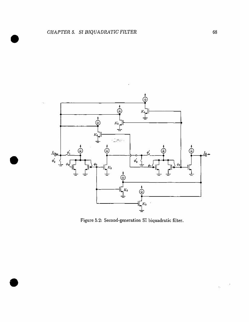
• CHAPTER 5. SI BIQUADRATIC FILTER
K, 11-------,
68
•
•
. :~,.;.,
,,p'l
Figure 5.2: Second-generation sr biquadratic filter.

•CHAPTER 5. SI BIQUADRATIC FILTER 69
•
gains are obtained by scaling the aspect ratios of the mirroring transistors Dccord
ingly. In addition, the current sources feeding these transistors are also scaled by the
sarne factor. The values of the different [( parameters are listed in Table 5.1 for casy
reference.
Coefficients Value1(1 1.08241(2 a1(3 0.29291(4 1.08241(5 1.08241(6 0.7654
Table 5.1: Coefficients of a second-order SI LP biquad.
According to [30], these parameters will give the following biquadratic tmnsfer
function:
,"'
T(z) = _0.2929z2 +0.5858z +0.2929Z2 +5.87 x 10⁻⁵ z +0.1715
(5.1)
•
By substituting the discrete-tirne variable z with e;wT, where j is the imaginary
nurnber, w the physical radian frequency and T the sampling clock period of 500
kHz, an ideal frequency response can be obtained for the first and second-generation
filters. This was perforrned by sweeping w between 0.1 and 0.1 MHz. The expected
frequency response is shown in Figure 5.3. The 3-dB frequency of the two filters was
found to be approximately equal to 125 kHz. It is our intention here to design an SI
circuit that has a frequency response sirnilar to this depicted one.

• CHAPTER 5. SI BIQUADRATIC FILTER
·20
iD -40
'"..0
"0
.,00':;,-'-'''-'''''c.,...........":'';',-'--'='J,,....w..w.":":;-........=";.<-'--'--''''',0:0• .-J1~ 10 10 10 10
freQl!ency (Hz)
70
• 5.2
Figure 5.3: Frequency response of the first and secondgeneration SI biquadratic filter with cutoff frequency ~
125kHz, clocked at 500 kHz.
Design of SI Biquadratic Filter
•,~..
The SI LP biquad gives a cutoff frequency of around 125 kHz with a clocking frequency
of 500 kHz. In order to implement these two SI filters in silicon, the size of the unit
transistor has to be first determined. From there, the sizes of other transistors can
be scaled according to Table 5.1.
In this section, a step-by-step guideline will be provided for the reader in order to
calculate the area of the unit-sized transistors and other parameters of the circuit so as
to obtain a near-optimum design. A second-generation regulated-cascode integrator
shown in Figure 5.4 will be used to illustrate the design procedure. Referring to
Figure 5.4, let us denote the drain currents f10wing into the main memory transistors
Ml and Mal as Id l and Id" respectively. Let us further assume that, without loss of
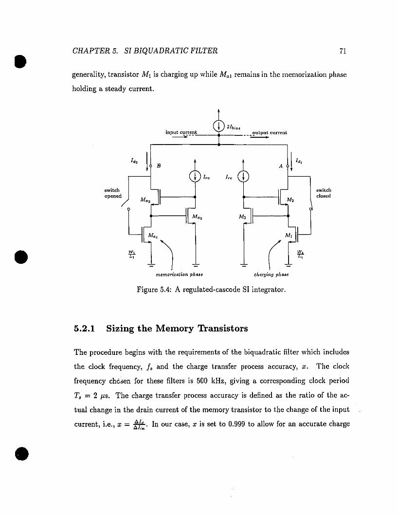
generality, transistor l'vIt is charging up while Mal remains in the memorizatioll phase• CHAPTER 5. SI BIQUADRATIC FILTER
holding a steady current.
inp~r~!1,,-t__+ .~ currcnt.
71
•
switchopened
B
+ 1re Ire
~ M.,
* '1memorization phase
II".
charginy pillue
Hwit.chc10acd
5.2.1
Figure 5.4: A regulated-cascode SI integrator.
Sizing the Memory Transistors
•
The procedure begins with the requirements of the biquadratic filter which includes
the dock frequency, J, and the charge transfer process accuracy, x. The dock
frequency chèsen for these filters is 500 kHz, giving a correspondillg dock period
TB = 2 floS. The charge transfer process accuracy is defined as the ratio of the ac
tuaI change in the drain current of the memory transistor to the change of the input
current, i.e., x = tf.:. In our case, x is set to 0.999 to allow for an accurate charge

transfer. These two numbers, f, and x, will be shown to be critical for subsequent
calcuJations.
• CHAPTER 5. SI BIQUADRATIC FILTER 72
(5.2)
•
(i) Settling Time: It was addressed in Chapter 2 that the charge transfer processes
of both the first and second-generation cells were governed by a single-time-constant
process with time-constants given by Eqn. (2.4) and (2.5), respeetively. In the case of
an SI integrator, it will have an identical settling behavior. Thus, the time constant
(Tint) becomesCg,
Tint=- ,gm
where Cg, and gm represent the total gate capacitance and the transconduetance
of transistor Ml in Figure 5.4 during the charging phase, respeetively. Given the
charge transfer accuracy of x = 0.999, together with the STC charging behavior of
the memory cell (refer to Chapter 2 for more details) mathem"tically we can write
the following constraint on the time constant of the integrator Tint:
t:..ld _..L...--=X < [1 - e Tint]t:..lin
_..L...0.999 < [1 - e T'nt]
===> Tint >T,
(5.3)/oge(O.OOI)
Wc can see from Eqn. (5.3) that Tint takes on its minimum value when it becomes
equal to the right-hand side of the equation. This is the situation when the dock
period is just large enough for the integrator to settle within the desired tolerance.
Thus, by substituting the values of T, and Tint using Eqn. (5.3), we can write
•gm 1 . _ _ /oge(O.OOI)
min -Cg, 2 J1.S
(5.4)
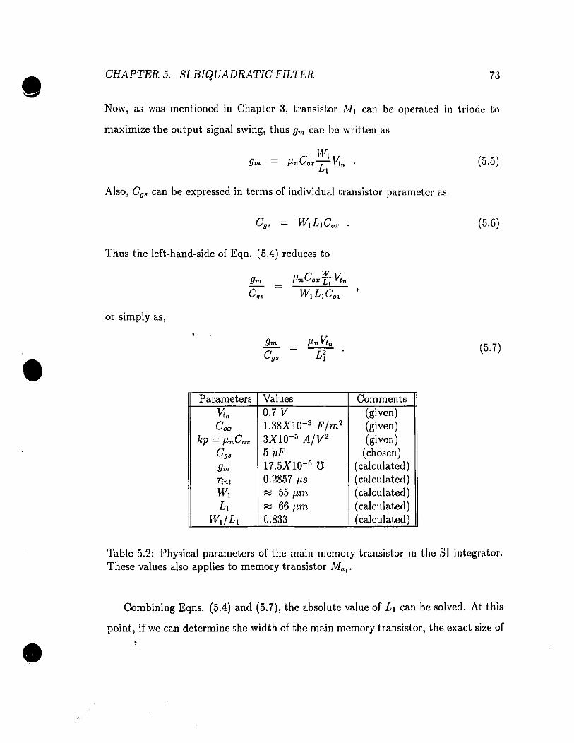
CHAPTER 5. SI BIQUADRATIC FILTER 73
Now, as was mentioned in Chapter 3, transistor Ml cau be operated 111 triode to
maximize the output signal swing, thus gm can be written as
(5.5)
Also, Cgs can be expressed in terms of individual transistor parameter as
(5.G)
Thus the left-hand-side of Eqn. (5.4) reduces to
C lli. \~= /ln ox LI l"
WlL1Cox
•or simp!y as,
=
Parameters Values Comments
VIn 0.7 V (given)Cox l.38XlQ-3 F/m2 (given)
kp = PnCox 3XI0-5 A/V2 (givcn)Cgs 5 pF (chosen)gm 17.5XI0-6 U (calculated)Tint 0.2857 ps (calculated)WI l'':j 55 pm (calculated)LI l'':j 66 J1.m (calculated)
WilL I 0.833 (calculated)
(5.7)
•
Table 5.2: Physical parameters of the main memory transistor in the sr integrator.These values ..Iso applies to memory transistor Ma,.
Combining Eqns. (5.4) and (5.7), the absolute value of LI can be solved. At this
point, if we can determine the width of the main memory transistor, the exact size of

transistor Ml (or equivalently Ma, since they are equal-sized) will have been found.
1'0 facilitate the calculation of the width of the memory transistor, agate capacitance
value of 5 pF was chosen. The area of this transistor was chosen such that the thermal
noise voltage at the gate of the memory transistor was insignificant. For example,
the thermal noise voltage-level corresponding to the 5 pF gate capacitance at room
tempera.ture can be calculated as follows:
=
Noiserms =
•CHAPTER 5. SI BIQUADRATIC FILTER
Jk~1.38 x 10-23 x 300
5 X 10-'2
f':; 28pV ,
74
•
•
which is deemed as insignificant in this case. As a result, W, can be calculated directly
from Eqn. (5.6). Skipping the remaining arithmetics, we summarize the results of the
above calculations for the memory transistor in Table 5.2. Also, the sizes of various
other transistors in the biquadratic filter are calculated simply by scaling the aspect
ratios according to the coefficients listed in Table 5.1. These sizes are listed in Table
5.3 for easy reference.
Coefficients Value Actual Transistor SizeK, 1.0824 59.53 pmi 66 pmK 2 0 not applicableK 3 0.2929 16.11 pmi 66 pm[(., 1.0824 59.53 pmi 66 pm[(5 1.0824 59.53 pmi 66 pmKG 0.7654 42.10 Ilml 66 pm
Table 5.3: Aspect ratios of transistors in SI L? biquad.
(ii) Current Swing: Another important aspect is the current handle capability of
the integrator. In order to maintain linear operation over the widest possible range of
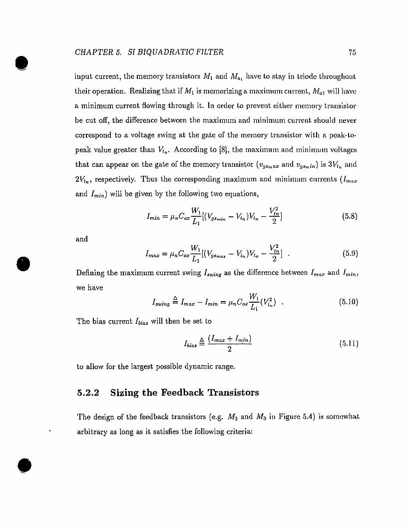
input carrent, the memory transistors MI and Mal have to stay in triode throughout
their operation. Realizing that if Ml is memorizing a maximum cUlTent, Pdal will have
a minimum current fiowing through it. In order to prevent either memory transistor
be cut off, the difference between the maximum and minimum current should never
correspond to a voltage swing at the gate of the memory transistor with a peak-to
peak value greater than \!ta' According to [8J, the maximurn and minimum voltages
that can appear on the gate of the memory transistor (vg•max and Vg"mi") is 3\~" and
2\!tn' respectively. Thus the corresponding maximum and minimum currents (/lUa"
and [min) will be given by the following two equations,
• CHAPTER 5. SI BIQUADRATIC FILTER
W \/21 . - C _1 [(Y: _ \1. ) \1. _..J!!.]mm - /ln oz L gSmin tn f" ?1 -
75
(5.8)
Defining the maximum carrent swing [swing as the difference between lma" and llUi" ,•and
[ - C WI[(y: _ \1. )\1, _ \1;;,]max - fLn or LI gSmll:f tn 11l 2 . (5.fJ)
we have
The bias current hia. will then be set to
[ t> (Imax + lmin)bias = 2
to allow for the largest possible dynamic range.
5.2.2 Sizing the Feedback Transistors
(5.10)
(5.11 )
•The design of the feedback transistors (e.g. M2 and Ms in Figure 5.4) is somewhat;
arbitrary as long as it satisfies the following criteria:
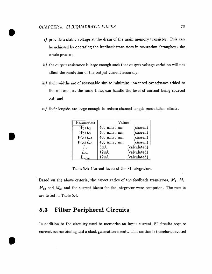
i) pI'ovide a stable voltage at the drain of the main memory transistor. This can
be achieved by operating the feedback transistors in saturation throughout the
whole process;
•CHAPTER 5. SI BIQUADRATIG FlLTER 76
•
•
ii) the output resistance is large enough such that output voltage variation will not
affect the resolution of the output CUiTent accuracy;
iii) their widths are of reasonable size to minimize unwanted capacitance added to
the ceIl and, at the same time, can handIe the level of current being sourced
out; and
iv) their lengths are large enough to reduce channel-Iength modulation effects.
Parameters ValuesW2fL2 400 pmf6 pm (chosen)WafLa 400 pmf6 pm (chosen)
WadLa2 400 pmf6 pm (chosen)WaafLaa 400 pmf6 pm (chosen)
Ire 6pA (calculated)Ibia.s 12pA (calculated)
[swing 12pA (calculated)
Table 5.4: Current levels of the SI integrators.
Based on the above criteria, the aspect ratios of the feedback transistors, M2, Ma,
Ma2 and Maa and the CUiTent biases for the integrator were computed. The results
are listed in Table 5.4.
5.3 Filter Peripheral Circuits
In addition to the circuitry used to memorize an input current, SI circuits require
ClllTent source biasing and a clock generation circuit. This section is therefore devoted

• CHAPTER 5. SI BIQUADRATIC FILTER
to the design of these peripheral filter circuits.
5.3.1 High-Swing Double-Cascode Current Source
77
•
R, Rs
to ol.hcl'cU8codcH
1.. ,,, 1 v.. ,,, < v+ - ""V
•
Figure 5.5: Righ-swing double-cascode current source.
Although there exists many different types of current sources, in this thesis, a
high-swing MOS current mirror [31] was adopted as the current source. This source
is unique because of its very high output resistance and large linear range'lf opera
tion; ideal for SI circuits. The CUITent source is shown in Figure 5..5. II; consists of
sorne equal-sized transistors with aspect ratios If = 12 pm/1.6 Ilm and sorne scaled
transistors with aspect ratios of ~ and ~. Reasons for such a choice of transistor
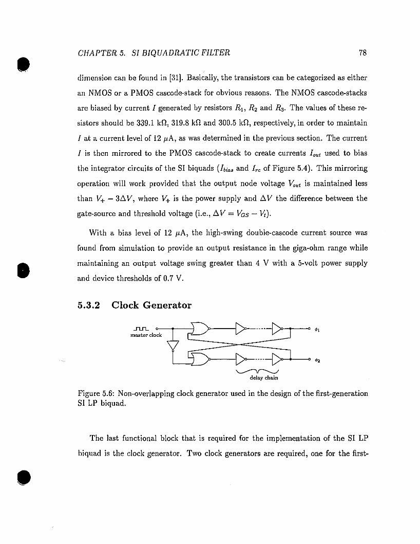
dimension can be found in [31J. Basically, the transistors can be categorized as either
an NMOS or a PMOS cascode-stack for obvious reasons. The NMOS cascode-stacks
•CHAPTER 5. SI BIQUADRATIC FILTER 78
•
are biased by current J generated by resistors RI, R2 and R3 • The values of these re
sistol'S should be 339.1 kn, 319.8 kn and 300.5 kn, respectively, in order to maintain
J at a CUITent level of 12 flA, as was determined in the pl'evious section. The current
J is then mil'rored to the PMOS cascode-stack to create currents Jout used to bias
the integrator circuits of the SI biquads (hi". and Jre of Figure 5.4). This mil'l'oring
operation will work pl'ovided that the output node voltage Vaut is maintained less
than V+ - 3.6.V, where V+ is the power supply and .6.V the difference between the
gate-source and threshold voltage (i.e., .6.V = Vas - 1~).
With a bias level of 12 flA, the high-swing double-cascode current source was
found from simulation to provide an output resistance in the giga-ohm range while
maintaining an output voltage swing greater than 4 V with a 5-volt power supply
and device thresholds of 0.7 V.
5.3.2 Clock Generator
J1..fLmastcr dock
•
~delay chain
Figure 5.6: Non-overlapping dock generator used in the design of the first-generationSI LP biquad.
The last functional block that is required for the implementation of the SI LP
biquad is the dock genera.tor. Two dock generators are required, one for the first-

•CHAPTER 5. SI BIQUADRATIC FILTER iD
generation biquad, the other for the second-generation one. The one used for thc nrst,
generation design is a simple two-phase non-overlapping dock generator as shown in
Figure 5.6. This circuit is commonly used to generate the appropriate dock signais
in SC circuits. An input dock signal, denoted as the master dock, is subdiviclcd
into two dock signaIs <Pl and <P2 with a non-overlapping interval dctermined by the
number of inverters in the delay chain. For example, using a chain of ten 20 11II1/
8pm inverter with a 0.85 ns delay each will give a non-overlapping interval of 8.5 ns.
•
.nn..master dock
,.,,
",
•
Figure 5.i: Modified dock generator used in the design of the second-generation SILP biquad.
For the second-generation biquad, a four-phase dock generator providing con
trolled dock signaIs similar to those described for the second-generation integrator of
section 4.2.2. The circuit used is shown in Figure 5.i. This second-generation dock
generator differs l'rom the one used in the first-generation circuit in that it has two
more inverters cascaded with the two output dock signais. These invel·ters, which
delay the original non-overlapping docks, will produce the two extra dock phases
required by the second-generation filter. The timing diagrams of the first and second
generation filters are shown in Figure 5.8(a) and (b).
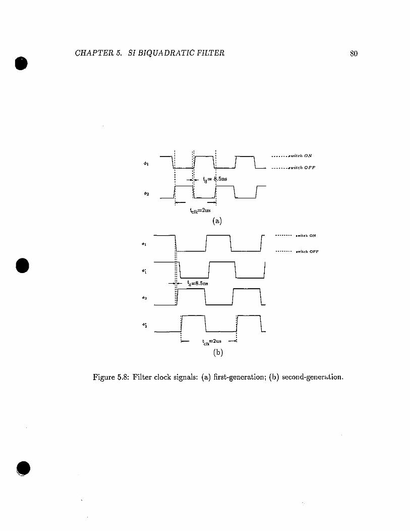
• CHAPTER 5. SI BIQUADRATIC FlI,TER SD
., ___ •••• .IIwitdION
•.••• __ .nl.ilcll DFf<'
•.,
.',
.,
.',
4::n?2us
(a)
-_ ...... Iwltch ON
~ 1 \ r ........ Iwheh 01"1"
11 \ 1 \ 1
litd=B.5ns
\ 1 l
1\
1 ll-- tc:Jk=2us ---l
(h)
•
Figure 5.8: Filter dock signais: (a) first-generationj (h) second-gencr~tion.
• CHAPTER 5. SI BIQUADRATIG FILTER
5.4 Layout and Fabrication
81
•
The two SI LP biquads were laid out in a 1.2 pm single-polysilicon double-metal
CMOS fabrication process (CMOS4S) of Northern Telecom Limited. The !Joor plans
of the fabricated designs are shown in Figure 5.9(a) and 5.10(a), respectively. The
resulting fabricated silicon prototypes, being part of a 40-pin chipl, are captured
as two micro-photographs, enlarged and displayed in Figure 5.9(b) and 5.10(b), ac
cordingly. Various building blocks can be easily identified when the floor plans and
micro-photographs are compared.
The SI filters were extracted from the two layouts to generate an HSPICE netlists.
These netlists contained not only the original circuit elements of the two SI filters,
but as well the parasitic components in the circuits. In order to simulate the layout.s
in frequency domain, the HSPICE netlists were translated to a WATSNAP netlist
using an in-house program, called SNAPER2• The results of these analyses are shown
in Figure 5.11.
Figure 5.11 shows a frequency response which is quite different from the one
depieted in Figure 5.3, particularly at the end of the passband and the beginning
of the stopband. This is an obvious example of Q-enhancementj the filter poles
shifting closer to the unit circle than intended. As we lower the clock frequency
down to 50 kHz, however, the frequency response resembles the intended one, as
shown in Figure 5.12. This phenomenon has been traced back to differences between
the transconduetances calculated in Table 5.2 and the actual ones used in the final
designs. Snch deviation is largely the result of an over-simplificatioll of transistor
lCanadian Microelectronics Corporation (CMC) imp!ementation run ID. MPC 9302CA, design!lames: ICAMGSIA and ICAMGSIB.
2SNAPER is a program developed at McGill University by Loai Louis and John Abcarius underthe supervision of Prof. Gordon Roberts.
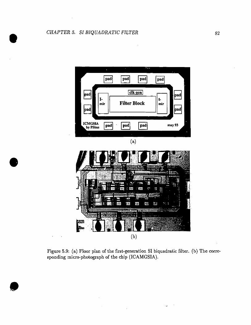
•
•
CHAPTER 5. SI BIQUADRATIC FILTER
(a)
(b)
82
•
Figure 5.9: (a) Floor plan of the first-generation SI biquadratic filter. (h) The corresponding micro-photograph of the chip (ICAMGSIA).
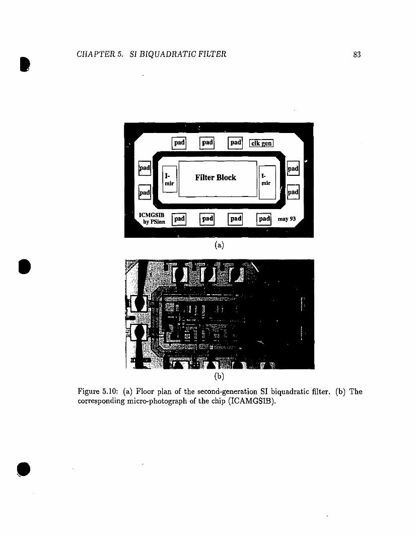
•
•
CHAPTER 5. SI BIQUADRATIC FILTER
(a)
(h)
83
•
Figure 5.10: (a) Floor plan of the second-generation SI hiquadratic filter. (h) Thecorresponding micro-photograph of the chip (ICAMGSIB).

•
•
•
CHAPTER 5. SI BIQUADRATIC FILTER
5
o
·5
iii-10e..~Cl-15
·20
·25
·30
Figure 5.11: Simulated frequency response of the two SIfilters with fclk = 500 kHz.
behavior used to select transistor dimension.
first-generation second-generationDesign ID ICAMGSIA ICAMGSIBDC Power (5V supply) 1.05 mW 0.82mWCurrent source (1) Arca 110/-lm X 430/-lm 100/-lm X 250/-lmCurrent source (II) Area 110/-lm X 430/-lm 120/-lm X 380/-lmFilter Area 1367/-lm X 600/-lm 1400/-lm X 544/-lmChip Area 2300/-lm X 1450/-lm 2300/-lm X 1450llm
Table 5.5: Area and power estimates.
Other expected highlights of the two chips have been summarized in Table 5..5.
Referring to the table, the two filters occupy almost the same amount of silicon but
dissipate different amounts of static power. The second-generation filter requires
approximately 20% less static power than the first-generation filter. The obvious

• CHAPTER 5. SI BIQUADRATIC FILTER 85
10
0
·10
;;;~.20.."
·30
·40
·5010'10' 102 10'
Fre~uBncy{Hz)
10' 10'
•
•
Figure 5.12: Simulated frequency response of the two SIfilters. fclk = 50 kHz and fadB = 12.5 kHz.
reason for this power saving cornes from the faet that the second-generation filter uses
fewer current sources. Although power optimization is not the main concern of this
work and the results obtained here are not easily generalized, it is interesting to note
that second-generation circuits may be more suitable for low-powered applications.
5.5 Summary of Fabrication Results
The experiments to be performed with the two test chips of SI biquads were originally
scheduled to include a De diagnostic pre-test whieh provides preliminary operating
condition of the chip, and a transient/spectral test which determines the funetionality
of the biquads and generates THD measurement results. Unfortunately, however, the
author is sorry to have identified that both chips ceased to functioH. A short between
supply and ground in the clock-generator circuit prevented the two circuits from
• CHAPTER 5. SI BIQUADRATIC FILTER
operating. As a result, no experiments could be cOlldllcted with them.
5.6 Conclusion
86
•
-,
In this chapter, practical issues for the design and layout of SI biquadratic filters
in a CMOS process were addressed. This included the dimensiol1ing of the various
transistors in the SI circuits, as weil as a description of other peripheral circuits, such
as the CUl'rent sources and clock generators. Test chips were fabricatec! using a j.2
/lm CMOS technology supplied by Northern Telecom LTD .. Unfortullately, the test
chips dic! not work and we couic! not validate the simulation results .

•
•
•
Chapter 6
Conclusion
The Switched-Current (SI) technique has been proposed as an alternative means to
the well-known Switched-Capacitor technique. Its superiority over the SC technique
stems from its compatibility to a standard digital CMOS process and current7mode
nature. The work of this thesis, being part of the on-going analog microelectronics
research at the Microelectronics And Computer Systems Laboratory, McGill Univer
sity [32], was devoted to the study of the underlying limitations and applicability of
the SI technique.
At the time of writing, largely because of its relatively short period of existence
in the field, there exists very few discussion in the open research literature on the
advantages and disadvantages of the SI technique. As one of the pioneers in the SI
circuit technique, the author has uncovered sorne of its major pitfalls. Undeniably,
this advancement in our understanding of the SI techniques is essential for its future
development at McGill University and, more globally, in the whole analog microelec
tronics community.
In the introduction to this dissertation, a brief history of the SI technique was
given together with a review of the ideal operation of the first and second-generation
87
• CHAPTER 6. CONCLUSION ss
•
•
SI memory cell. This led into Chapter 2 where the non-ideal operation of the two
cells was outlined. Apart from the common errors which resulted from imperfcct.
behavior of MOS transistors, a discussion on the sensitivity behavior of each ccli was
provided. Contrary to what was generally believed, the first and second-generation
memory cells were shown to have exactly the same sensitivity behavior to component
variations, except in the case when the second-generation cell is used in a unity-gain
configuration. Unfortunately, this situation is rare in practice and was thus conduded
in Chapter 2 that both cells have essentially the same sensitivity behaviorj one could
not be favored over the other for this reason alone. On the other hand, a serious
problem of signal glitching was discovered with the second-generation memory ccli.
This motivated the author to perform an extensive HSPICE simulation of the two
cells in Chapter 3 and study the effect of this glitching on the operation of the cell.
On doing so, it was discovered that the second-generation memory ccli produced
large levels of distortion. This was traced back to the existence of a high-impedancc
node that appeared during the non-overlapping interva.\ of the 2-phase dock. A 3
phase dock scheme was therefore proposed, together with the incorporation of the
regulated-cascode configuration, in order to remedy this problem. With such circuit
enhancements, the second-generation memory ccli operated more linear but was still
out-performed by its first-generation counterpart.
In Chapter 4, the performance comparison was extended to SI delay cells and
integrators. The same glitching problem described in Chapter 3 was also present in
these second-generation circuits. In the case of SI integrators, a 4-phase dock scheme
was introduced 'to shorten the existence of the high-impedance node. Computer
simulations demonstrated that this approach is indeed viable. Unfortunately, in the
case of SI delay cells, no new dock scheme could be found that would minimize the

• CHAPTER 6. CONCLUSION 89
•
glitching. It was therefore concluded that the second-generation SI delay cel! should
not be used in linear circuit applications.
Aiming at sorne silicon prototypes to provide experimental confirmation of the
simulation results, the design of two different SI biquadratic filters was outlined in
Chapter 5. One biquad was based on the first-generation memory cel! and the other
on the second-generation memory cel!. Practical design issues were brought forward,
such as the calculation of sizes of transistors, details of the current biasing scheme
and the dock generation circuit. As one of the first designers to fabricate a SI filter
circuit at McGil! University, it was unfortunate that the resulting chip when returned
from fabrication did not function. This had prevented the author from confirming
our arguments with solid experimental results. Nonetheless, the investigation carried
out was performed using sound simulation techniques and should be valid for most
SI circuits.
6.1 Future Work /,1
•
Although in recent years we have seen an explosion of research activities into SI
circuits [28J, there is undoubtedly much to learn about the SI technique.
For one, in order to overtake commercial SC designs, SI circuits must be capable
of providing equal or better performance than its SC counterpart. One of the issues
not addressed in this thesis but critical to present day sampled-data circuits is the
overall noise behavior of SI circuit. To date, very little research has been conducted
in this direction.
Secondly, more silicon prototypes are needed to confirm the validity of the SI
technique. The benefits of such an approach would be two-fold. Firstly, it uncovers

• CHAPTER 6. CONCLUSION 90
•
•
circuit artifaets that are lacking in present day simulations. Secondly, and probably
the most important, operational prototypes would be all the more convincing to
industry in what the sr technique has to offer.
To wrap up this thesis, it is the author's belief that the sr technique will be one
of the hottest analog sampled-clata techniques in this decacle.
•
•
•
Bibliography
[1] R. Gregorian, G. A. Wegner and W. E. Nicholson, "An Integrated Single-Chip
PCM Voice Codee with Filters," IEEE Journal of Solid-State Circuits, vol. SC
16, no. 4, pp. 322-333, Aug. 1981.
[2] P. R. Grey and R. Castello, "Performance Limitations in Switched-Capacitor
Filters," Design of MOS VLSI Circuits for Telecommuncations, Prentice-Hall,
pp. 314-332, 1985.
[3] R. Gregorian and G. C. Ternes, Analog MOS !ntegrated Circuits for Signal Pro
cessing, Wiley, New York, USA 1986.
[4] P. K. Chatterjee and G. B. Larrabee, "Gigabit age microelectronics and their
manufacture," IEEE Transactions on VLSI Systems, vol. 1, no. 1, pp. 7-21,
March 1993.
[5] J. H. Huijsing, R. Hogervorst and K. J. de Langen, "Low-Voltage Low-Power
Amplifiers," IEEE International Symposium on Circuits and Systems Proceed
ings, pp. 1443-1446, May 1993.
[6] J. B. Hughes, N. C. Bird and 1. C. Macbeth, "Switched currents - a new technique
for analog sampled-data signal processing," IEEE International Symposium on
Circuits and Systems Proceedings, pp. 1584-1587, May 1989.
91
• BIBLIOGRAPHY 92
•
•
[7] S. J. Daubert, D. Vallancourt and Y. P. Tsividis, "Current copier cells," Elec
tronics Letters, vol. 24, pp. 1560-1562, 1988.
[8] G.W. Roberts and P. J. Crawley, "Building Blocks For Switched-Current Sigma
Delta Modulators," in Switched-Curl'eni Techniques For Analogue VLSI, C.
Toumazou, J. B. Hughes and N. Battersby (Editors), Peter Peregrinus Limited,
London, England, pp. 350-380, 1993.
[9] 1. Song, Switched-Current Filters using Bilinear Integrators, Master Thesis, De
partment of Electrical Engineering, Faculty of Graduate Studies, McGiIl Univer
sity, 1994, in preparation.
[10] P. J. Crawley and G. W. Roberts, "Switched-Current Sigma-Delta Modulation
for A/D Conversion," IEEE International Symposium on Circuits and Systems
Proceedings, pp. 1320-1323, May 1992.
[11] J. B. Hughes, 1. C. Macbeth and D. M. Pattullo, "Second generation switched
current signal processing," IEEE International Symposium on Circuits and Sys
tems Proceedings, pp. 2805-2808, May 1990.
[12] T. S. Fiez and D. J. Allstot, "CMOS switched-current ladder filters," IEEE
Journal of Solid-State Circuits, vol. 25, no. 6, pp. 1360-1367, Dec. 1990.
[13] J. B. Hughes and K. W. Moulding, "Switched-Current Signal Processing for
Video Frequencies and Beyond," IEEE Journal of Solid-State Circuits, vol. 28,
No. 3, March, 1993, pp. 314-322.
[14] N. C. Battersby and C. Toumazou, "A 5th Order Bilinear Elliptic Switched
Current Filter," Proceedings of IEEE Custom Integrated Circuits Conference,
6.3.1-4, May 1993.

• BIBLIOGRAPHY 93
•
•
[15J G. W. Roberts and A. S. Sedra, "Synthesizing switched-current filters by trans
posing the SFG oï switched-capacitor filter circuits," IEEE Transaction on Cir
cuits and Systems, vol. CAS-38, pp. 337-340, March 1991.
[16] A. C. M. de Queiroz, P. R. M. Pinheiro and L. P. Calôba, "Systematic Nodal
Analysis of Switched-Current Filters," IEEE International Symposium on Cir
cuits and Systems Proceedings, pp. 1801-1804, May 1991.
[17] WATSNAP Users' Guide, University of Waterloo, Canada, 1992.
[18J P. M. K. Sinn and G. W. Roberts, "A Performance Comparison of First and
Second Generation Switched-Current Structures for Analog Sampled-Data Sig
nal Processing," IEEE International Symposium on Circuits and Systems Pro
ceedings, pp. 301-304, May 1994.
[19] D. MacQuigg, "Residual Charge on a Switched-Capacitor," IEEE Journal of
Solid-State Circuits, vol. SC-18, pp. 811-813, Dec. 1983.
[20J B. J. Sheu'and C. Hu, "Switched-induced Error Voltage on a Switched
Capacitor," IEEE Journal of Solid-State Circuits, vol. SC-19, pp. 519-525, Aug.
1984.
[21] J. Shieh, M. Patil and B. J. Sheu, "Measurement and Analysis of Charge Injection
in MaS Analog Switches," IEEE Journal of Solid-Stat Circuits, vol. SC-22, no.
2, pp. 277-281, Apr. 1987.
[22] R. C. Yen and P. R. Gray, "A MaS Switched-Capacitor Instrumentation Am
plifier," IEEE J. Solid-State Circuits, vol. SC-l7, no. 6, pp. 1008-1013, Dec.
1982.
•
•
•
BIBLIOGRAPHY
[23] G. Wegmann and E. A. Vittoz, "Very accurate dynamic current mirrors," Elcc
tronics Letters, vol. 2.5, pp. 644-646, May 1989.
[24]H. C. Yang, T.S. Fiez and D..J. Allstot, "Current-Feedthrough Effects and Can
cellation Techniques in Switched-Current Circuits," IEEE International Sympo
sium on Circuits and Systems Proceedings, pp. 3186-3188, May 1990.
[25J Paul R. Gray and Robert G. Meyer, Analysis and Design of Analog lntcgmted
Circuits, Wiley, New York, 1993.
[26J C. Toumazou, J. B. Hughes and D. M. Pattullo, "Regulated Cascode Switchcd
Current Memory Cell," Electronic Letters, vol. 26, no. 5, pp. 303-305, Mar. 1990.
[27J P..1. Crawley and G. W. Roberts, "Predicting Harmonic Distortion [n Switchcd
Current Memory Circuits," IEEE Transactions on Circuits and Systems -[: Fun
damental Theory and Applications, vol. 41, no. 2, pp. 73-86, Feb. 1994.
[28J C. Toumazou, J. B. Hughes and N. C. Battersby (Editors), Switchcd-Cul'rents:
an analogue technique for digital technology, Peter Peregrinus Limited, London,
England, 1993.
[29J A. C. M. de Queiroz and P. R. M. Pinheiro, "Switching Sequence Effects in
Switched-Current Filters," IEEE International Symposium on Circuits and Sys
tems Proceedings, pp. 982..985, May 1993.
[30] A. S. Sedra and G. W. Roberts, "Sampled-Data Analog Filters," in ANA
LOG VLSI: Signal and Information Processing, M. Ismail and T. Feiz (Editors),
McGraw-Hill Inc., New York, New York, pp. 307-359, 1993.
[31J P..1. Crawley and G. W. Roberts, "High-swing MOS current mirror with arbi
trarily high output resistance," Electronics Letters, vol. 28, no.4, pp. 361-363,
Feb. 1992.
•BlBUOGRAPHY 95
•
•
[32] "PROGRESS REPORT 1993 - Microelectronics And Computer Systems Labo
ratory", Micl'oelectronics And Computer System Laboratory, McGill University,
1993.
[33J Alan V. Oppenheim, Discrele-time Signal Processing, Englewood Cliffs, N.J.:
Prentice Hall, 1989.

•
•
Appendix A
Spectral Analysis with HSPICE
Throughout the work of this thesis, the Power Spectral Oensity (l'SO) of a signal
was used as the bases of performance comparison between different SI structures.
With on-bench testing, the l'SO of a signal can be obtained diredly from a Spedrum
Analyzer (e.g. HP 3588A) with little difficulty. ln contrast, the mcthod of extrading
spectral measurement from an HSPICE transient analysis requires special care. This
appendix will outline how to setup the input deck so that l'diable PSO measurements
can be obtained using the transient analysis capability of nSPICE, together with a
Fast Fourier Transform (FFT) alogrithm [33].
A.l HSPICE Input Deck
•
For illustrative purposes, the HSPICE simulation deck of the first-generation SI cur
rent memory cell is displayed in Figure A.l. The circuit schematics of this circuit
would be similar to that of Figure 3.1 (a) with a sampled-and-hold circuit as its
input. The output current is extracted through a OC voltage source whose levd
maintains the output transistor in saturation. The input deck in Figure A.1 begins
with the Circuit Description which includes the transistor model extracted from
96

•
•
•
APPENDIX A. SPECTRAL ANALYSIS WITH HSPICE
POWER SPECTRAL ANALYSIS of SI Current Memory CeU
*** Circuit Description **** transistor models *.model model3 nmos level=2 Vlo =0.8l99V l'd=33.26 1'3=33.26 i3=le-16+ pb=0.8 cgso =1.973e-IO cgdo=3.284e-IO cgbo=940e-12 Cj=0.0004l+ mj=0.540 cjsw=3.4e-IO mj3w=0.30 j3=0.0001 tox=2.502e-8+ nsub=1.983e+16 nss=O.OOO nfs=2.98ge+12 tpg=l xj=58.4le-09 ld=147.5e-09+ uo=378.4 ucri,=lOOOO uexp=0.2550 vmox=3.642e+04 neJJ=1.8l5+ fc=0.5 delta=1.10l* control docks *V~ <p 0 pulse(5 0 LOu O.Olu O.Olu 0.98u 2u)V~ ~ 0 pulse(O 5 LOu O.Olu O.Olu 0.98u 2u)* input sampled-and-held signal *VIN 11 0 sin(O 1 20k)9in 11 12 ~ 0 level=l min=5 max=lg 19 -0.2g *ideal switchCs1l 12 0 Ip91 1 0 12 0 10/-1Vi 1 20Cg, 20 O.Olp* current memory cell *h, 0 2 20/-1Ml 2 2 0 0 w= 400/-1 1= 60/-1Mdummy, 2 <p 3 0 model3 w=4/-1 1=1.2/-1Mdummy, 3 ~ 3 0 model3 w=2/-1 1=1.2/-1M2 4 3 0 0 w= 400/-1 1= 60/-1h, 0 4 20/-1* output current measurement *Vlo". 4 0 1.174688V
*** Analysis Request ***.option numdgt=7 ingold=2.op.tran 2/-1s l250/-ls 50.95/-1s IOns
*** Output Request ***.print tran i(Vi) i(V;o".).end
Figure A.l: HSPICE input deck of the first-generation SI memory cell.
97
• APPENDIX A. SPECTRAL ANALYSIS WITH HSPICE 98
the Northern Telecom 1.2ILm CMOS fabrication process. This model is applied to ail
the transistors in the circuit. The l'est of the circuit description is the circuit netlist,
which gives a one-to-one correspondence with the SI circuit elements.
Following the circuit netlist is the Analysis Request section. This sedion go\'
erns the environment under which the simulation is to be performed and commanels
the simulator to perform a specific analysis. It will be explained in duc comse that
the request for transient analysis has to be handled with great care if reliable l'SD
measurements are to be obtained. The HSl'ICE input cleck ends with the Output
Request section. This section is usecl to generate the desirecl data points of the input,
or output signais.
In order to obtain meaningful PSD measurements from a transient simulation, special
care must be taken in generating the data points. A step-by-step guicle is proviclecl
below basedon the method suggested by Crawley and Roberts in [27].
•A.2 Setting U p The Transient Analysis
•
The procedure begins by selecting the radix, N, of the FFT alogrithm. This
algorithm is used to transform the transient data points into the frequency clomain.
In [27], a 2-point FFT was chosen as a special case. Here we will clemonstrate how
the PSD can be computed using a radix of N = 5. Choosing a number larger than 2
as the raclix will decrease the number of data points usecl in the analysis. But apart
from this,'~~ other advantage is obtained by selecting N greater than 2.
Step 1 Choose the input signal period Tin such that it is a multiple of the dock periocl
T and that ~ = Nn, where n is an integer greater than zero. Therefore, if the
dock frequency is 500 kHz, and the frequency of the input current is set to 20

•APPENDIX A. SPECTRAL ANALYSIS WITH HSPICE
kHz, then we find that n = 2.
99
•
•
Step 2 Determine the total number of periods of the output signal that need to be sim
ldated. This should be a power of N, i.e., number of period = Nm, where
m is an integer. This will in turn determine the frequency resolution of the
PSD measurement. In our case, if m = 2, the total number of points in the
power spectrum equals Nn+m = 625. With a 500 kHz dock, this leads to a
frequency separation of exactly 800 Hz. Of course, a more refined resolution
can be obtained at the expense of longer simulation time.
8tcp 3 Choosc the starting time to record the data points. Since the circuit needs time
to reach steady-state, it is not proper to collect data points during the initial
transient period. In our case, the circuit was found to settle with reasonable
accuracy after the first period of the input signal. Therefore, the starting time
of the recording begins immediately after the first period of the input signal, Le.
50.95 /-IS. In order to collect the correct samples, as weil as provide maximum
time for the circuit to settle, the input signal was sampled at the end of dock
phase </>1, Similarly, the output was sampled at the end of dock phase </>2, half
a dock period later (i.e. 1/-15).
Following the above procedure, the transient analysis statement for input signal
15
.tran 2/-15 1300/-15 50.95/-15 IOns
while the corresponding statement of the output signal is
.tran 2/-15 1300/-15 51.95/-15 IOns
In both statements, the first number signifies the incremental time interval for simula
tion, the second and third numbers denote the ending and starting time, respectively,
and the last number determines the maximum time step allowed in the simulator.
•APPENDIX A. SPECTRAL ANALYSIS HlITH liSPICE 100
•
•
Performing the HSPICE simulation twice, one for each transient analysis state
ment given above, the sampled data is ready for the radix-5 1"1"'1' alogrithm.