original citation - wrap: warwick research archive...
TRANSCRIPT

warwick.ac.uk/lib-publications
Original citation: Marshall, Kenneth, Walker, Marc, Walton, Richard I. and Hatton, Ross A.. (2016) Enhanced stability and efficiency in hole-transport-layer-free CsSnI3 perovskite photovoltaics. Nature Energy, 1. 16178. Permanent WRAP URL: http://wrap.warwick.ac.uk/84013 Copyright and reuse: The Warwick Research Archive Portal (WRAP) makes this work by researchers of the University of Warwick available open access under the following conditions. Copyright © and all moral rights to the version of the paper presented here belong to the individual author(s) and/or other copyright owners. To the extent reasonable and practicable the material made available in WRAP has been checked for eligibility before being made available. Copies of full items can be used for personal research or study, educational, or not-for-profit purposes without prior permission or charge. Provided that the authors, title and full bibliographic details are credited, a hyperlink and/or URL is given for the original metadata page and the content is not changed in any way. Publisher’s statement: http://dx.doi.org/10.1038/nenergy.2016.178 A note on versions: The version presented here may differ from the published version or, version of record, if you wish to cite this item you are advised to consult the publisher’s version. Please see the ‘permanent WRAP URL’ above for details on accessing the published version and note that access may require a subscription. For more information, please contact the WRAP Team at: [email protected]
1
Enhanced Stability and Efficiency in Hole-Transport Layer Free CsSnI3
Perovskite Photovoltaics
K. P. Marshall1, M. Walker2, R. I. Walton1, and R. A. Hatton1*
1Department of Chemistry, University of Warwick, CV4 7AL, UK.
2Department of Physics, University of Warwick, CV4 7AL, UK.
Abstract
Photovoltaics based on tin halide perovskites have not yet benefitted from the same
intensive research effort that has propelled lead perovskite photovoltaics to >20% power
conversion efficiency, due to the susceptibility of tin perovskites to oxidation, the low energy
of defect formation and the difficultly in forming pin-hole free films. Here we report CsSnI3
perovskite photovoltaic devices without a hole-selective interfacial layer that exhibit a
stability 10 times greater than devices with the same architecture using methylammonium
lead iodide perovskite, and the highest efficiency to date for a CsSnI3 photovoltaic: 3.56%.
The latter results in large part from a high device fill-factor, achieved using a strategy that
removes the need for an electron blocking layer or an additional processing step to minimise
the pinhole density in the perovskite film, based on co-depositing the perovskite precursors
with SnCl2. These two findings raise the prospect that this class of lead-free perovskite
photovoltaic may yet prove viable for applications.
2
Introduction
Lead-free perovskite photovoltaics (PPVs) using tin halide as the light harvesting
semiconductor have not yet benefitted from the same intensive research effort that has
propelled lead PPVs from a power conversion efficiency (of 3.8% in 20091 to >20%
today2, because of the susceptibility of tin to oxidation from the 2+ to the 4+ oxidation states
upon exposure to air, a transformation that does not occur easily in lead perovskites.3,4
Consequently, the record for tin halide PPVs lags behind that of lead PPVs at 6%,
achieved using CH3NH3SnI3 sandwiched between a mesoporous TiO2 hole-blocking layer
(HBL) and doped spiro-OMeTAD electron blocking layer (EBL).5,6 The low energy of
formation of tin array vacancies in tin halide perovskites has also proved problematic,
making it difficult to achieve high device fill-factor (FF) due to high rates of defect mediated
charge carrier recombination.7,8 Similar to the case of lead perovskites, a further challenge
has been in achieving solution processed thin films of tin perovskites with a low density of
pin-hole defects, to avoid undermining device FF.9 Beyond being lead-free, tin halide
perovskites offer a number of properties which make them attractive for use in PPVs
provided the challenge with stability can be addressed, including narrower band gaps than
their lead analogues (1.3-1.4 eV)10,11, low exciton binding energies (18 meV)12,13 and high
charge mobilities11,14,15.
To date reports relating to the use of tin halide perovskites as the light harvester in
PPV devices5,6,8,9,16–21 are relatively few in number, and the has primarily been limited by a
sub-optimal FF.5,6,8 Kumar et al.8 have shown that PPVs based on CsSnI3 sandwiched
between a TiO2 HBL and triphenylamine EBL (FF ~ 0.3) are stable when stored under
nitrogen, although the stability in air and/or under continuous illumination was not reported.
Hao et al.6 have shown that after 24 hours under nitrogen the of devices based on
CH3NH3SnI3 sandwiched between a TiO2 HBL and spiro-OMeTAD EBL (FF ~ 0.48) was
reduced by 64%, even with encapsulation. Similarly, Noel et al.5 reported that PPVs based
on CH3NH3SnI3 with the same charge selective interlayers (FF 0.5) degrade within minutes
3
when tested under ambient conditions, and Zhang et al.21 have reported that unencapsulated
PPV devices based on HC(NH2)2SnI2Br, using PEDOT:PSS and PC61BM charge extraction
layers, failed within minutes of exposure to air.
Recently we have shown how the efficiency of PPV devices based on the black
polymorph of CsSnI3 perovskite; (B)- CsSnI3, sandwiched between a fullerene HBL and
copper iodide EBL, can be improved by incorporating an excess of SnI2 into the CsSnI3 film19
- The B- phase is of most relevance for photovoltaic applications because it exists below
89°C.11 Unfortunately, the stability of those devices was relatively poor with a 30% loss in
when stored in the dark in ambient air for 1 hour.19 Herein we have extended this
investigation to explore the potential of SnF2, SnCl2 and SnBr2 additives in CsSnI3 based
PPVs, which has yielded some important new findings that enable the device fabrication
process and architecture to be simplified, whilst simultaneously greatly increasing . We
show that SnCl2 stands out as being a particularly beneficial additive, and that simplifying
device architecture by removing the EBL dramatically improves device stability. Crucially,
removal of the EBL layer does not reduce device when SnCl2 additive is co-deposited with
the CsSnI3 layer.
Probing B- CsSnI3 film structure and stability
It is known that B- CsSnI3 degrades to the zero-dimensional Sn(IV) salt Cs2SnI6 in ambient
air and that the absorption coefficient of Cs2SnI6 in the visible spectrum is a factor of 10
times smaller than that of B-CsSnI3.14 Consequently, it is possible to monitor the oxidation
of thin films of CsSnI3 in air by measuring the evolution of the electronic absorption spectrum
with time, as shown in Figures 1a and 1b.
4
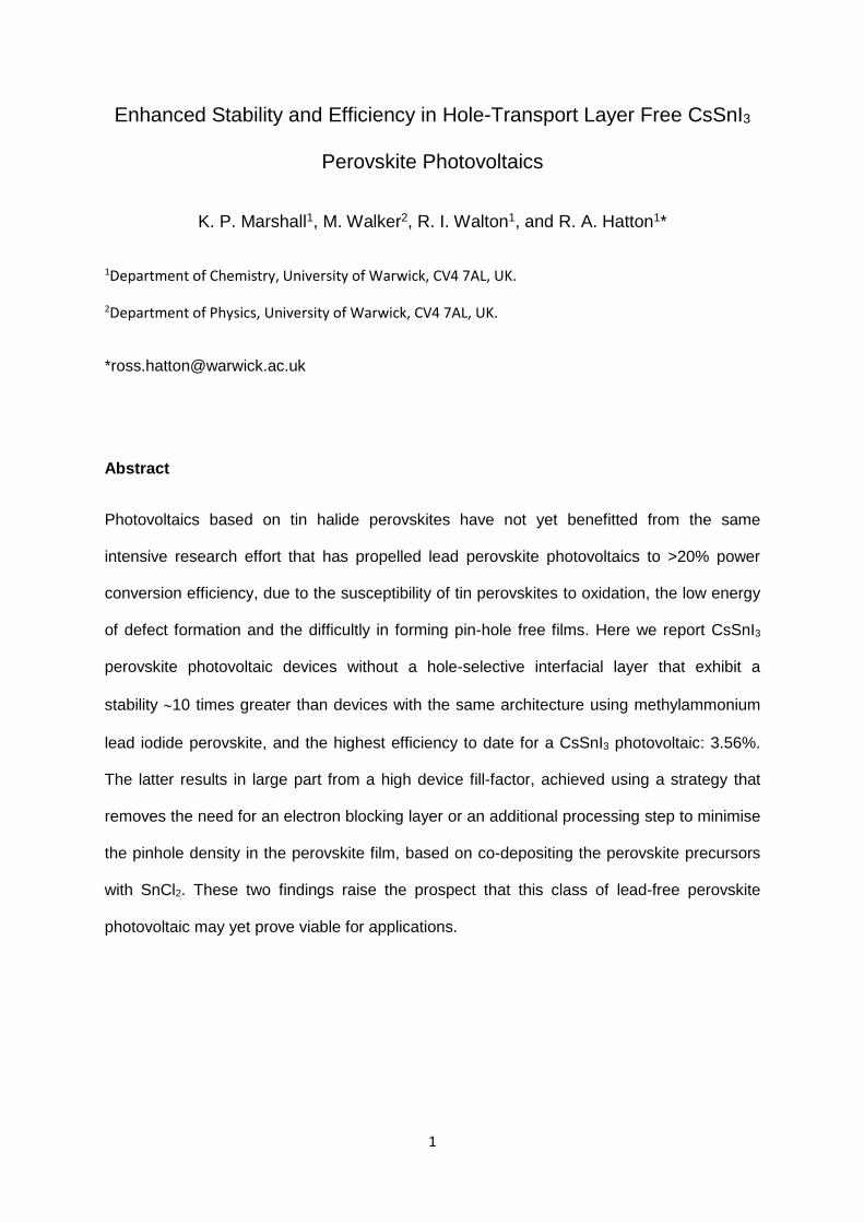
Figure 1 | Evolution of the absorption spectrum of CsSnI3 films with different tin halide
additives in ambient air. a CsSnI3; b CsSnI3 + 10% SnCl2; and c normalised absorbance at
500 nm for CsSnI3 with 10 mol% of SnI2, SnBr2, SnCl2 or SnF2, and with no tin halide
additive. In all cases the CsSnI3 solution concentration was 8 wt% which resulted in a film
thickness of 50 nm. All films supported on indium tin oxide (ITO) coated glass. The red
vertical lines indicate the direction of change with increasing time in ambient air. [See
Supplementary Discussion]
It is evident from Figure 1c that of the four tin halides investigated SnCl2 results in the
highest film stability. Based on the time taken for the absorbance at 500 nm to reduce by
30%, films with SnCl2 are more stable by a factor of 3.7 times as compared to CsSnI3 films
with 10 mol% excess SnI2, and a factor of 6.7 times compared to films with no tin halide
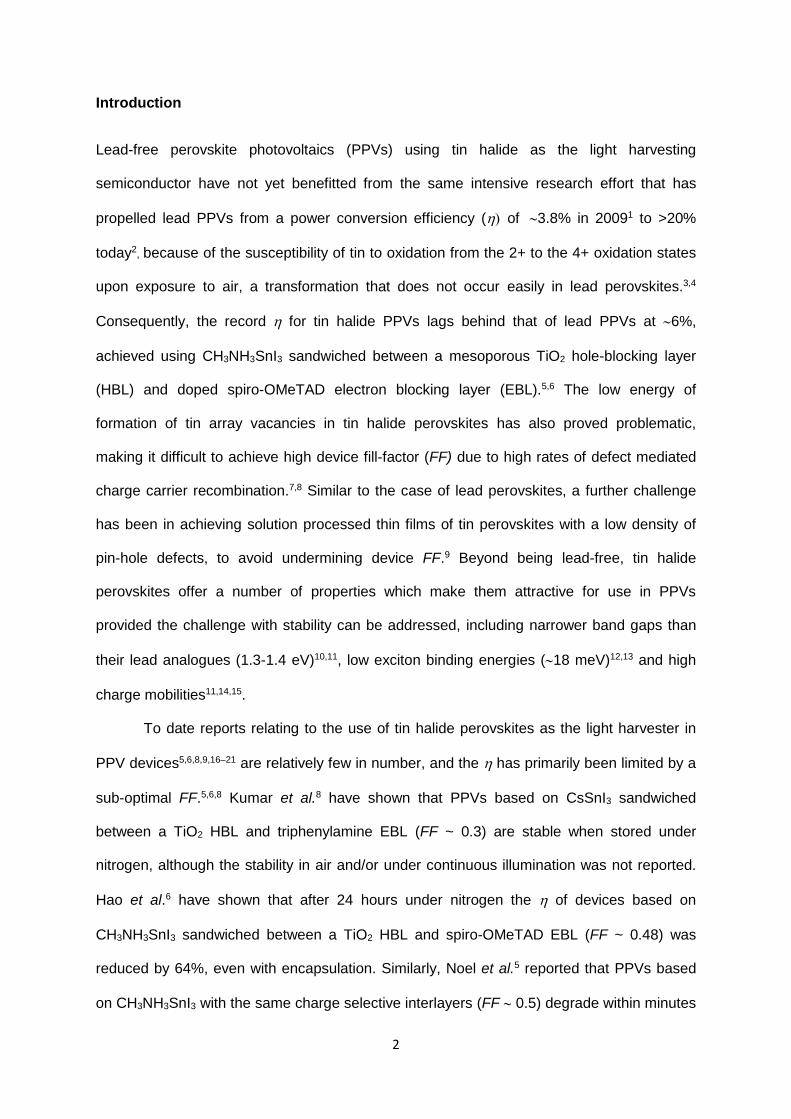
additive. The scanning electron microscope (SEM) images in Figure 2 show that the former
cannot be attributed to a difference in film porosity because films prepared with 10 mol%
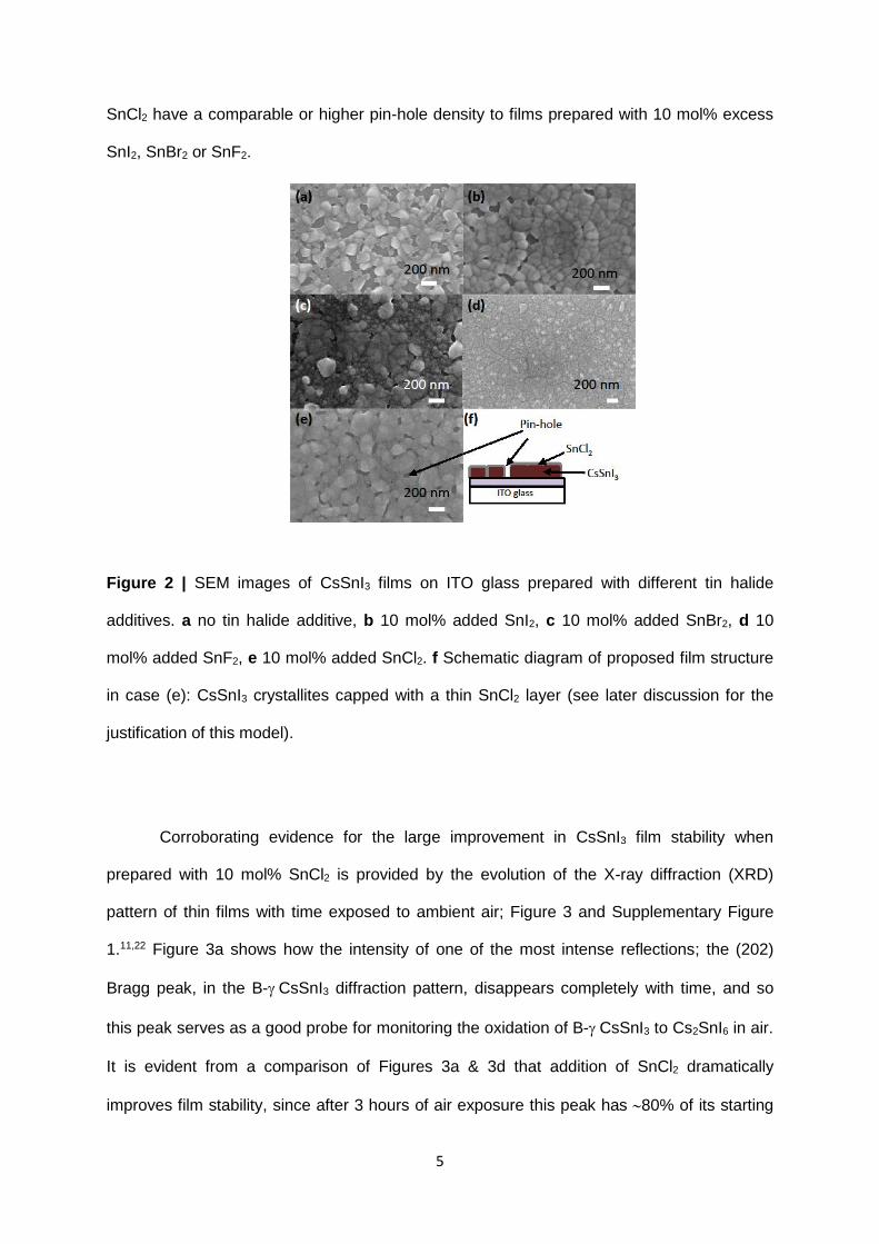
5
SnCl2 have a comparable or higher pin-hole density to films prepared with 10 mol% excess
SnI2, SnBr2 or SnF2.
Figure 2 | SEM images of CsSnI3 films on ITO glass prepared with different tin halide
additives. a no tin halide additive, b 10 mol% added SnI2, c 10 mol% added SnBr2, d 10
mol% added SnF2, e 10 mol% added SnCl2. f Schematic diagram of proposed film structure
in case (e): CsSnI3 crystallites capped with a thin SnCl2 layer (see later discussion for the
justification of this model).
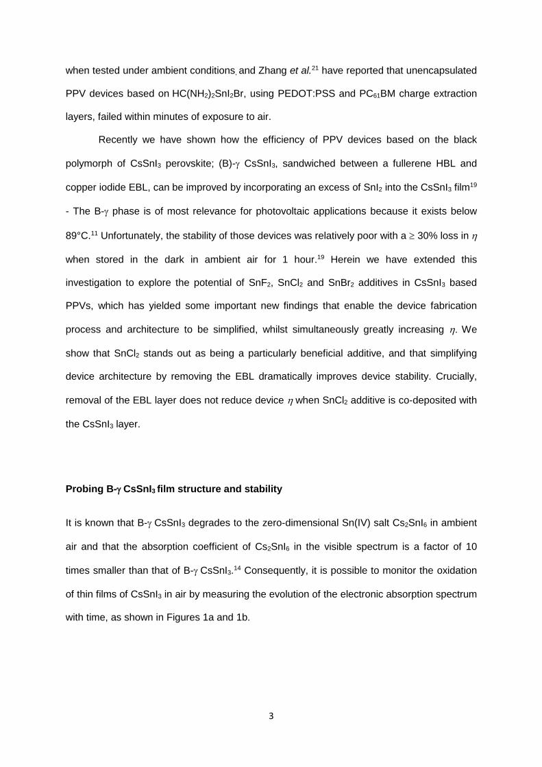
Corroborating evidence for the large improvement in CsSnI3 film stability when
prepared with 10 mol% SnCl2 is provided by the evolution of the X-ray diffraction (XRD)
pattern of thin films with time exposed to ambient air; Figure 3 and Supplementary Figure
1.11,22 Figure 3a shows how the intensity of one of the most intense reflections; the (202)
Bragg peak, in the B-CsSnI3 diffraction pattern, disappears completely with time, and so
this peak serves as a good probe for monitoring the oxidation of B-CsSnI3 to Cs2SnI6 in air.
It is evident from a comparison of Figures 3a & 3d that addition of SnCl2 dramatically
improves film stability, since after 3 hours of air exposure this peak has 80% of its starting
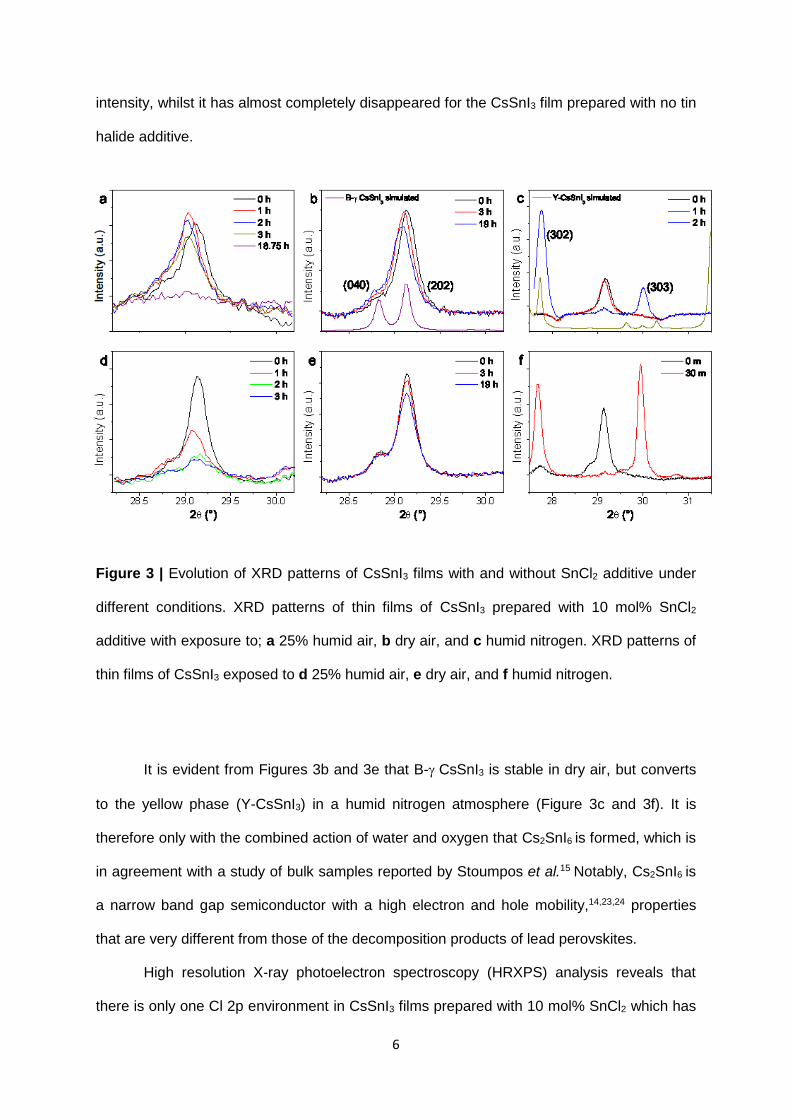
6
intensity, whilst it has almost completely disappeared for the CsSnI3 film prepared with no tin
halide additive.
Figure 3 | Evolution of XRD patterns of CsSnI3 films with and without SnCl2 additive under
different conditions. XRD patterns of thin films of CsSnI3 prepared with 10 mol% SnCl2
additive with exposure to; a 25% humid air, b dry air, and c humid nitrogen. XRD patterns of
thin films of CsSnI3 exposed to d 25% humid air, e dry air, and f humid nitrogen.
It is evident from Figures 3b and 3e that B- CsSnI3 is stable in dry air, but converts
to the yellow phase (Y-CsSnI3) in a humid nitrogen atmosphere (Figure 3c and 3f). It is
therefore only with the combined action of water and oxygen that Cs2SnI6 is formed, which is
in agreement with a study of bulk samples reported by Stoumpos et al.15 Notably, Cs2SnI6 is
a narrow band gap semiconductor with a high electron and hole mobility,14,23,24 properties
that are very different from those of the decomposition products of lead perovskites.
High resolution X-ray photoelectron spectroscopy (HRXPS) analysis reveals that
there is only one Cl 2p environment in CsSnI3 films prepared with 10 mol% SnCl2 which has
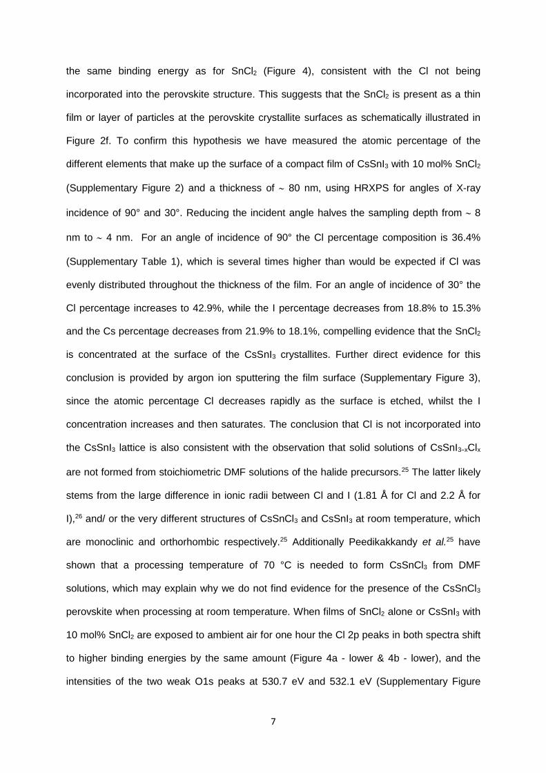
7
the same binding energy as for SnCl2 (Figure 4), consistent with the Cl not being
incorporated into the perovskite structure. This suggests that the SnCl2 is present as a thin
film or layer of particles at the perovskite crystallite surfaces as schematically illustrated in
Figure 2f. To confirm this hypothesis we have measured the atomic percentage of the
different elements that make up the surface of a compact film of CsSnI3 with 10 mol% SnCl2
(Supplementary Figure 2) and a thickness of 80 nm, using HRXPS for angles of X-ray
incidence of 90° and 30°. Reducing the incident angle halves the sampling depth from 8
nm to 4 nm. For an angle of incidence of 90° the Cl percentage composition is 36.4%
(Supplementary Table 1), which is several times higher than would be expected if Cl was
evenly distributed throughout the thickness of the film. For an angle of incidence of 30° the
Cl percentage increases to 42.9%, while the I percentage decreases from 18.8% to 15.3%
and the Cs percentage decreases from 21.9% to 18.1%, compelling evidence that the SnCl2
is concentrated at the surface of the CsSnI3 crystallites. Further direct evidence for this
conclusion is provided by argon ion sputtering the film surface (Supplementary Figure 3),
since the atomic percentage Cl decreases rapidly as the surface is etched, whilst the I
concentration increases and then saturates. The conclusion that Cl is not incorporated into
the CsSnI3 lattice is also consistent with the observation that solid solutions of CsSnI3−xClx
are not formed from stoichiometric DMF solutions of the halide precursors.25 The latter likely
stems from the large difference in ionic radii between Cl and I (1.81 Å for Cl and 2.2 Å for
I),26 and/ or the very different structures of CsSnCl3 and CsSnI3 at room temperature, which
are monoclinic and orthorhombic respectively.25 Additionally Peedikakkandy et al.25 have
shown that a processing temperature of 70 °C is needed to form CsSnCl3 from DMF
solutions, which may explain why we do not find evidence for the presence of the CsSnCl3
perovskite when processing at room temperature. When films of SnCl2 alone or CsSnI3 with
10 mol% SnCl2 are exposed to ambient air for one hour the Cl 2p peaks in both spectra shift
to higher binding energies by the same amount (Figure 4a - lower & 4b - lower), and the
intensities of the two weak O1s peaks at 530.7 eV and 532.1 eV (Supplementary Figure
8
4(b)), assigned to SnO227 and H2O, respectively, is increased by 10-fold. The insight as to
the differing roles of water and oxygen provided by the XRD patterns, together with the
changes in the XPS spectra upon exposure to air, are consistent with the SnCl2 surface
layer functioning as a desiccant which sacrificially oxidises slowing the oxidation of the
underlying CsSnI3 by H2O, since SnCl2 is known to form a stable hydrate (SnCl2·2H2O) as
well as oxidising to form SnO2.28
Figure 4 | HRXPS Cl 2p spectra of films of SnCl2 and CsSnI3 + 10 mol% SnCl2 before and
after exposure to ambient air. a SnCl2 with and without 1 hour of air exposure; b CsSnI3 + 10
mol% SnCl2 with and without 1 hour of air exposure. The measured spectra, peak
deconvolution and the sum of the fitted peaks are given by black, red and blue lines
respectively. Fitting performed using CasaXPS software (see Methods Section). Peak
positions and intensities labelled on figures.
Photovoltaic device studies
To test if the improvement in film stability towards air exposure translates into improved
stability in PPVs, devices with a simplified architecture were fabricated, based on a planar
heterojunction using PC61BM as the HBL and CsSnI3 as the light harvesting layer. This
9
structure simplifies device fabrication and reduces the number of parallel degradation
pathways that can complicate the interpretation of device stability studies. A simplified
architecture is also attractive from a commercial perspective, since fabrication costs typically
increase with increasing number of processing steps.29 Of the four additives; SnCl2, SnI2,
SnBr2 and SnF2, PPV devices using SnBr2 and SnF2 exhibited poor device performance with
0.4% (Supplementary Table 2) and/or poor device yield and so were not investigated
further. Initially SnCl2 loadings of 5, 10 and 15 mol% were investigated (Supplementary
Figure 5 and Supplementary Table 3), and a loading of 10 mol% was found to give the
highest yield of working devices combined with a narrow photocurrent spread. Consequently
10 mol% tin halide is the additive loading used in all studies hereafter described. Importantly,
the current-voltage characteristics of devices recorded in forward and reverse sweep for a
range of starting voltages and scan rates exhibit no significant hysteresis (Supplementary
Figure 6).
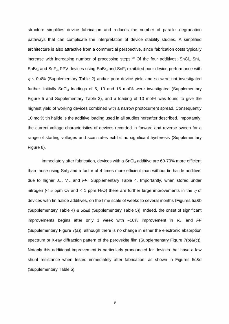
Immediately after fabrication, devices with a SnCl2 additive are 60-70% more efficient
than those using SnI2 and a factor of 4 times more efficient than without tin halide additive,
due to higher Jsc, Voc and FF; Supplementary Table 4. Importantly, when stored under
nitrogen (< 5 ppm O2 and < 1 ppm H2O) there are further large improvements in the of
devices with tin halide additives, on the time scale of weeks to several months (Figures 5a&b
(Supplementary Table 4) & 5c&d (Supplementary Table 5)). Indeed, the onset of significant
improvements begins after only 1 week with 10% improvement in Voc and FF
(Supplementary Figure 7(a)), although there is no change in either the electronic absorption
spectrum or X-ray diffraction pattern of the perovskite film (Supplementary Figure 7(b)&(c)).
Notably this additional improvement is particularly pronounced for devices that have a low
shunt resistance when tested immediately after fabrication, as shown in Figures 5c&d
(Supplementary Table 5).
10
Figure 5 | Current-voltage (JV) characteristics of CsSnI3 PPVs before and after a period of
extended storage under nitrogen. Representative JV characteristics for devices with the
structure: ITO|CsSnI3|PC61BM|BCP|Al using CsSnI3 with 10 mol% SnCl2, 10 mol% SnI2 and
with no additive as the light harvesting layer and PC61BM as the HBL. Devices were tested
immediately after fabrication (a and c) and after storage under nitrogen for an extended
period (b and d).
To our knowledge the FF is the highest achieved for a tin halide PPV; mean value of 0.63
and champion value of 0.69, which is particularly impressive given that there is no EBL and
the perovskite film has a high density of pinholes (Figure 2e). Furthermore, whilst CsSnI3
films with 10 mol% SnCl2 prepared from 8 wt% solution have a much greater density of
pinholes than those prepared from 16 wt% solution (Supplementary Figure 8), the device FF
is improved (Supplementary Figure 9 and Supplementary Table 6), consistent with the SnCl2
preventing electrons moving from the PC61BM into the ITO electrode.
The simplest possible explanation for the improved device performance with SnCl2
additive is that the SnCl2 forms a > 1 nm thick hole-selective layer at the ITO|CsSnI3
interface. However, ultra-violet photoelectron spectroscopy (UPS) measurements
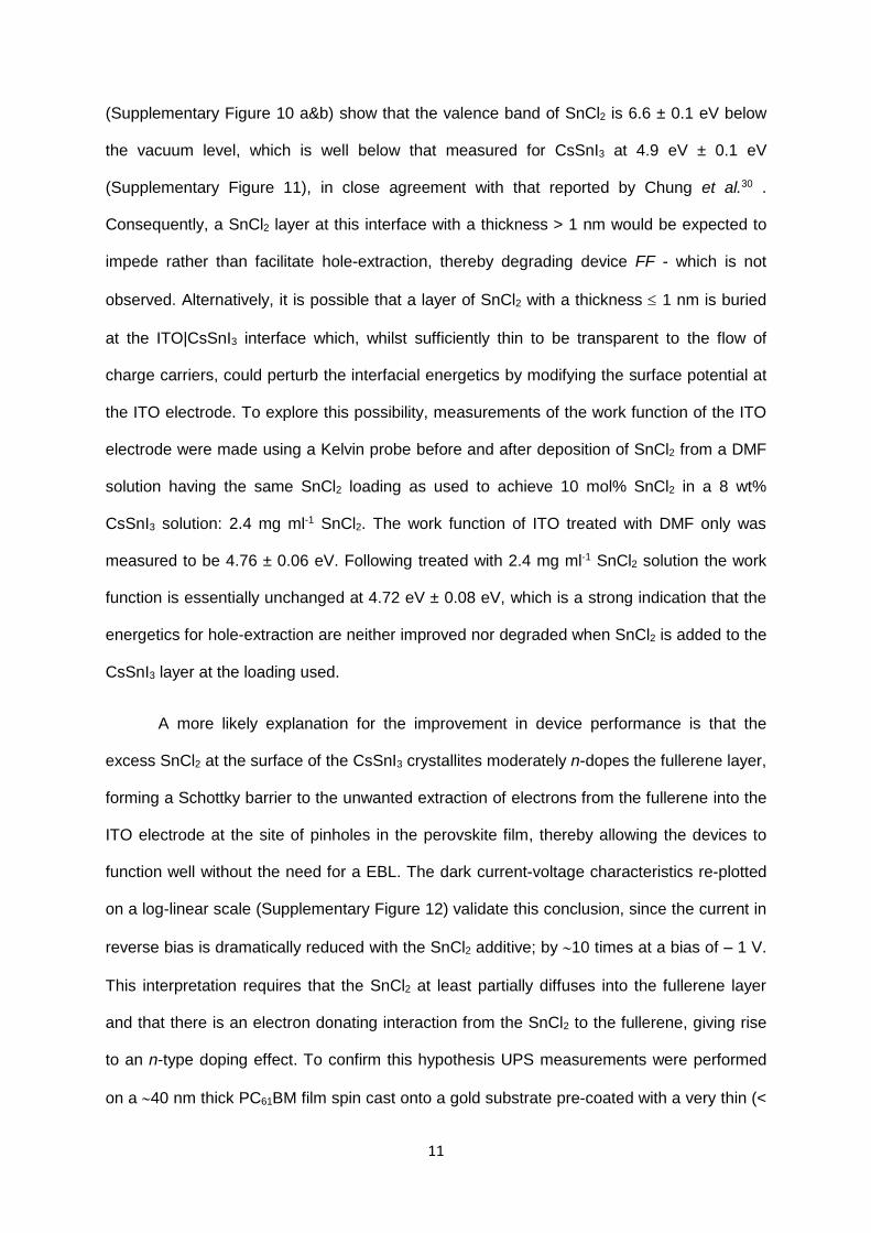
11
(Supplementary Figure 10 a&b) show that the valence band of SnCl2 is 6.6 ± 0.1 eV below
the vacuum level, which is well below that measured for CsSnI3 at 4.9 eV ± 0.1 eV
(Supplementary Figure 11), in close agreement with that reported by Chung et al.30 .
Consequently, a SnCl2 layer at this interface with a thickness > 1 nm would be expected to
impede rather than facilitate hole-extraction, thereby degrading device FF - which is not
observed. Alternatively, it is possible that a layer of SnCl2 with a thickness 1 nm is buried
at the ITO|CsSnI3 interface which, whilst sufficiently thin to be transparent to the flow of
charge carriers, could perturb the interfacial energetics by modifying the surface potential at
the ITO electrode. To explore this possibility, measurements of the work function of the ITO
electrode were made using a Kelvin probe before and after deposition of SnCl2 from a DMF
solution having the same SnCl2 loading as used to achieve 10 mol% SnCl2 in a 8 wt%
CsSnI3 solution: 2.4 mg ml-1 SnCl2. The work function of ITO treated with DMF only was
measured to be 4.76 ± 0.06 eV. Following treated with 2.4 mg ml-1 SnCl2 solution the work
function is essentially unchanged at 4.72 eV ± 0.08 eV, which is a strong indication that the
energetics for hole-extraction are neither improved nor degraded when SnCl2 is added to the
CsSnI3 layer at the loading used.
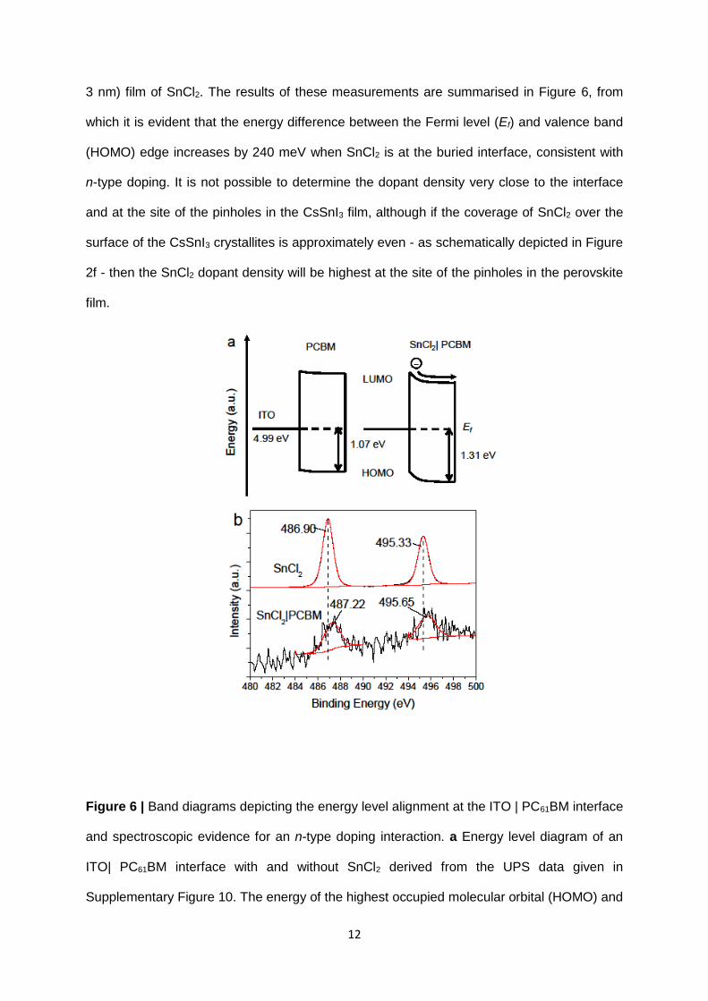
A more likely explanation for the improvement in device performance is that the
excess SnCl2 at the surface of the CsSnI3 crystallites moderately n-dopes the fullerene layer,
forming a Schottky barrier to the unwanted extraction of electrons from the fullerene into the
ITO electrode at the site of pinholes in the perovskite film, thereby allowing the devices to
function well without the need for a EBL. The dark current-voltage characteristics re-plotted
on a log-linear scale (Supplementary Figure 12) validate this conclusion, since the current in
reverse bias is dramatically reduced with the SnCl2 additive; by 10 times at a bias of – 1 V.
This interpretation requires that the SnCl2 at least partially diffuses into the fullerene layer
and that there is an electron donating interaction from the SnCl2 to the fullerene, giving rise
to an n-type doping effect. To confirm this hypothesis UPS measurements were performed
on a 40 nm thick PC61BM film spin cast onto a gold substrate pre-coated with a very thin (<
12
3 nm) film of SnCl2. The results of these measurements are summarised in Figure 6, from
which it is evident that the energy difference between the Fermi level (Ef) and valence band
(HOMO) edge increases by 240 meV when SnCl2 is at the buried interface, consistent with
n-type doping. It is not possible to determine the dopant density very close to the interface
and at the site of the pinholes in the CsSnI3 film, although if the coverage of SnCl2 over the
surface of the CsSnI3 crystallites is approximately even - as schematically depicted in Figure
2f - then the SnCl2 dopant density will be highest at the site of the pinholes in the perovskite
film.
Figure 6 | Band diagrams depicting the energy level alignment at the ITO | PC61BM interface
and spectroscopic evidence for an n-type doping interaction. a Energy level diagram of an
ITO| PC61BM interface with and without SnCl2 derived from the UPS data given in
Supplementary Figure 10. The energy of the highest occupied molecular orbital (HOMO) and
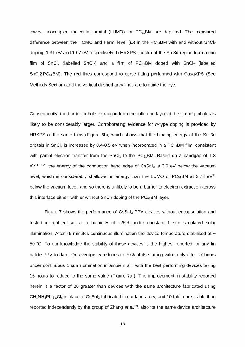
13
lowest unoccupied molecular orbital (LUMO) for PC61BM are depicted. The measured
difference between the HOMO and Fermi level (Ef) in the PC61BM with and without SnCl2
doping: 1.31 eV and 1.07 eV respectively. b HRXPS spectra of the Sn 3d region from a thin
film of SnCl2 (labelled SnCl2) and a film of PC61BM doped with SnCl2 (labelled
SnCl2PC61BM). The red lines correspond to curve fitting performed with CasaXPS (See
Methods Section) and the vertical dashed grey lines are to guide the eye.
Consequently, the barrier to hole-extraction from the fullerene layer at the site of pinholes is
likely to be considerably larger. Corroborating evidence for n-type doping is provided by
HRXPS of the same films (Figure 6b), which shows that the binding energy of the Sn 3d
orbitals in SnCl2 is increased by 0.4-0.5 eV when incorporated in a PC61BM film, consistent
with partial electron transfer from the SnCl2 to the PC61BM. Based on a bandgap of 1.3
eV11,15,25 the energy of the conduction band edge of CsSnI3 is 3.6 eV below the vacuum
level, which is considerably shallower in energy than the LUMO of PC61BM at 3.78 eV31
below the vacuum level, and so there is unlikely to be a barrier to electron extraction across
this interface either with or without SnCl2 doping of the PC61BM layer.
Figure 7 shows the performance of CsSnI3 PPV devices without encapsulation and
tested in ambient air at a humidity of 25% under constant 1 sun simulated solar
illumination. After 45 minutes continuous illumination the device temperature stabilised at ~
50 °C. To our knowledge the stability of these devices is the highest reported for any tin
halide PPV to date: On average, reduces to 70% of its starting value only after 7 hours
under continuous 1 sun illumination in ambient air, with the best performing devices taking
16 hours to reduce to the same value (Figure 7a)). The improvement in stability reported
herein is a factor of 20 greater than devices with the same architecture fabricated using
CH3NH3PbI3-xClx in place of CsSnI3 fabricated in our laboratory, and 10-fold more stable than
reported independently by the group of Zhang et al.29, also for the same device architecture
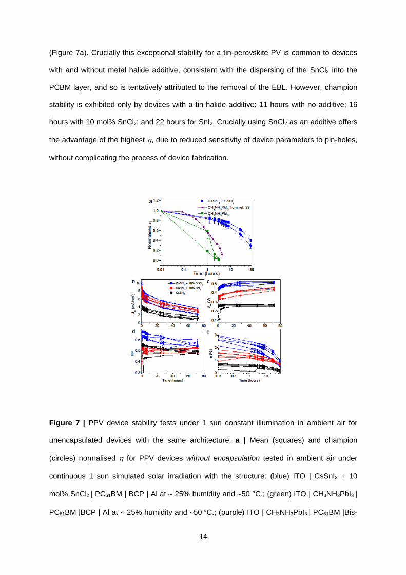
14
(Figure 7a). Crucially this exceptional stability for a tin-perovskite PV is common to devices
with and without metal halide additive, consistent with the dispersing of the SnCl2 into the
PCBM layer, and so is tentatively attributed to the removal of the EBL. However, champion
stability is exhibited only by devices with a tin halide additive: 11 hours with no additive; 16
hours with 10 mol% SnCl2; and 22 hours for SnI2. Crucially using SnCl2 as an additive offers
the advantage of the highest , due to reduced sensitivity of device parameters to pin-holes,
without complicating the process of device fabrication.
Figure 7 | PPV device stability tests under 1 sun constant illumination in ambient air for
unencapsulated devices with the same architecture. a | Mean (squares) and champion
(circles) normalised for PPV devices without encapsulation tested in ambient air under
continuous 1 sun simulated solar irradiation with the structure: (blue) ITO | CsSnI3 + 10
mol% SnCl2 | PC61BM | BCP | Al at 25% humidity and 50 °C.; (green) ITO | CH3NH3PbI3 |
PC61BM |BCP | Al at 25% humidity and 50 °C.; (purple) ITO | CH3NH3PbI3 | PC61BM |Bis-
15
C60 | Ag reported in Ref. 29. Error bars are ± 1 standard deviation. A linear-linear plot of this
data is also given in Supplementary Figure 13. b-e | Evolution of JV characteristics for a
representative set of unencapsulated devices tested in air under continuous 1 sun simulated.
The devices have the structure: ITO glass / CsSnI3 + X / PC61BM / BCP / Al, where X = 10
mol% SnCl2 (blue), 10 mol% SnI2 (red) or no additive (black). The temperature under the
lamp stabilised at 50 °C after 45 minutes continuous illumination. All curves are guides to
the eye.
It is evident from Figure 7 (b-e) that most of the degradation in device is due to
loss in Jsc, whilst FF is very stable and Voc actually increasing by 10% for all devices. The
increase in Voc can be attributed to the improved crystallisation in the fullerene layer that
occurs when the device is subject to intense light for an extended period, which reduces the
number of LUMO tail states that erode Voc32,33 and/or partial oxidation of the electrode to
form a very thin low work function aluminium oxide layer. The good stability in device FF
indicates that the series resistance in these devices does not change significantly as the light
harvesting ability deteriorates. This observation is consistent with the fact that Cs2SnI6 is a
weak absorber of light and has a high electron mobility23,34, and is compelling evidence that
the barriers to electron transport across the CsSnI3 / Cs2SnI6 and Cs2SnI6 / PC61BM are
small. That is, the Cs2SnI6 layer that forms at the CsSnI3/fullerene interface as a result of air
oxidation allows electron transport, whilst not significantly contributing to light harvesting.
The fact that devices with and without SnCl2 have nearly comparable stability, in
conjunction with evidence for n-type doping of the fullerene layer, indicates that in devices
the SnCl2 is no longer confined at the CsSnI3 surface but is dispersed in the adjacent
fullerene layer. Further evidence for this, and for a significant interaction between SnCl2 and
PC61BM, is provided by the electronic absorption spectra shown in Supplementary Figure
14, which shows how the absorbance of a 50 nm thick CsSnI3 film prepared with 10 mol%
16
SnCl2 at a wavelength of 450 nm changes with time exposed to ambient air, with and without
a PC61BM overlayer. It is evident that the CsSnI3 with 10 mol% added SnCl2 becomes less
stable when buried beneath a layer of PC61BM which is consistent with partial removal of the
SnCl2 from the perovskite surface. Conversely, Supplementary Figure 14b shows that
washing with chlorobenzene has no detrimental effect on the perovskite film stability, which
together is compelling evidence for a strong interaction between PC61BM and SnCl2.
Notably, whilst the Al electrode is evidently able to slow the ingress of water and oxygen into
the device sufficiently for a stability study on the time scale reported herein - consistent with
lifetime studies of organic PV devices using a very similar HBL35 – its long term barrier
properties are limited.35 It is anticipated that further significant improvements in device
stability can be achieved by using an electron extracting electrode with better barrier
properties towards ambient water and oxygen.
Discussion
Taken together the aforementioned experiments provide compelling evidence that SnCl2 is
the best of the tin halides investigated for the current application. The reason for this is
almost certainly a complex interplay between a number of factors including the following: (i)
Firstly, Cl cannot easily displace I in CsSnI3 perovskite, due to the size mismatch of the two
halides, and so SnCl2 is pushed to the surface of the crystallites, whilst still ensuring that the
perovskite is formed in a tin-rich environment.; (ii) SnCl2 is much more soluble in common
solvents, including DMF, than SnF2 due to its greater covalency, which is particularly
important when processing films from solution at room temperature, as in our fabrication
method.; (iii)The propensity for solid-state diffusion of tin chloride into fullerene is likely to be
larger due to the smaller size and lower mass of chloride species compared to the iodide
and bromide analogues.
17
In summary, a strategy for fabricating CsSnI3 based photovoltaic devices with the
highest fill factor reported for a tin PPV has been described, that simultaneously removes the
requirement for an electron blocking layer at the hole-extracting electrode and the need for
an additional processing step to minimise the density of pinholes in the perovskite film. We
have shown that the improved performance and tolerance to pin-holes in the perovskite film
stems from n-doping of the fullerene electron-transport layer by SnCl2, and that the stability
of unencapsulated CsSnI3 devices based on a simplified EBL free device architecture is
improved by at least an order of magnitude as compared to lead based PPV with the same
architecture when tested under continuous simulated solar illumination in ambient air at
50°C. Taken together, the findings reported herein justify an intensive research effort into tin
perovskite PVs, focused on improving to a level comparable to that of lead perovskite PVs.
Methods
Materials
CsI (Sigma-Aldrich 99.9%), SnI2 (Alfa Aesar, 99.999%), SnCl2 (Sigma Aldrich, 99.99%),
SnF2 (Acros Organics, 99%), SnBr2 (Alfa Aesar, 99.4%), Perovskite Precursor Ink (for
nitrogen processing) (Ossila, 1:1:4 PbCl2:PbI2:CH3NH3I, 99.999%:99.999%:99%, 99.8%
DMF), PC61BM (Solenne, 99.5%), bathocuproine (BCP) (Alfa Aesar, 98%), N,N-
dimethylformamide (DMF) (VWR, anhydrous, 99.8%), chlorobenzene (Sigma-Aldrich,
anhydrous, 99.8%), acetone (Sigma-Aldrich, GPR, 99%), propan-2-ol (Sigma-Aldrich, HPLC,
99.8%), deionised H2O (purite dispenser, >10 M). CsI and non-anhydrous solvents were
stored in air. All other chemicals were stored in a nitrogen filled glove box (<5 ppm O2 and
<1 ppm H2O).
18
B- CsSnI3 films
In a dry nitrogen filled glovebox CsI, SnI2 and tin(II) halide were mixed together in 1:1:0.1
molar ratio. To this mixture N,N-dimethylformamide (DMF) was added to make an 8 wt.%
solution (total mass of solids), which was stirred overnight before use. To deposit films, two
drops of solution were cast onto a substrate spinning at 4000 rpm for 60 seconds. The B-
phase forms immediately upon solvent evaporation.
Device fabrication
Indium tin oxide (ITO) coated glass slides (Thin Films Devices Inc. 15 ± 3 /sq.) were held in
vertical slide holders and ultra-sonically agitated in an acetone bath, followed by a high purity
water bath with a few drops of surfactant, followed by high purity deionized water only bath,
and finally an isopropanol bath. After this, the slides were suspended in hot acetone vapour
for 10 seconds before UV/O3 treatment for 15 minutes.
Immediately after UV/O3 treatment the slides were transferred into a dry nitrogen
filled glovebox for CsSnI3 film deposition, followed by deposition of a PC61BM film from 15
mg/ml chlorobenzene solution using a spin speed of 1500 rpm. The substrates were then
loaded into a high vacuum thermal evaporator located in the same glovebox and 6 nm of
bathocuproine (BCP) was deposited followed by 50 nm of Al at a pressure of 1×10⁻⁵ mbar
(with substrate rotation). The Al electrode was deposited through a shadow mask to make
six devices per slide, each with an area of 6 mm2.
Device Testing
Device testing was performed in the same glove box as used for device fabrication or, as for
the stability testing, using a solar simulator outside the glove box. Current density–voltage
(JV) curves were measured using a Keithley 2400 source-meter under AM1.5G solar
illumination at 100 mW/cm2 (1 sun), scanned from −1 V to +1 V at 0.1 V/s. Devices exhibited
no significant hysteresis (Figure S6). External quantum efficiency (EQE) measurements
19
were carried out using a Sciencetech SF150 xenon arc lamp and a PTI monochromator, with
the monochromatic light intensity calibrated using a Si photodiode (Newport 818-UV). The
incoming monochromatic light was chopped at 180 Hz. For signal measurement a Stanford
Research Systems SR 830 lock-in amplifier was used.
X-ray Diffraction (XRD)
XRD was performed on thin films of CsSnI3 prepared from 16 wt.% (total solids) DMF
solution deposited onto a substrate spinning at 4000 rpm for 60 seconds. A thicker film than
used in the devices was used here to obtain sufficient signal for the time dependent studies.
Scans were recorded under a flow of gas (dry nitrogen, dry air, humid nitrogen or ambient
air) using a Cu K/2 source in - mode on a Bruker D8 Advance powder diffractometer
equipped with an Anton-Paar HTK900 gas chamber. Humid nitrogen was introduced by
bubbling through water before the chamber. The measured XRD patterns were corrected for
height offset (due to the thickness of the film) by calibrating the 2 scale with reference the
expected peak positions for pure B-CsSnI3. Simulated diffraction patterns were calculated
using the program Mercury 3.1 using CIFs from the Inorganic Crystal Structure Database
(ICSD).
X-ray / Ultraviolet Photoelectron Spectroscopy
XPS was performed on film on gold coated glass substrates using a Kratos AXIS Ultra DLD.
Samples were unavoidably exposed to air for approximately 1 minute during transfer from an
air tight box to the vacuum chamber of the instrument. XPS measurements were carried out
in a UHV system with a base pressure of 5×10–11 mbar. The sample was excited with X-rays
from a mono-chromated Al K source (h = 1486.7 eV) with the photoelectrons being
detected at a 90° take-off angle. The sputtering was carried out at room temperature using a
Minibeam I ion gun (Kratos Analytical, UK). A beam of 4 keV Ar+ ions were incident on a 3
3 mm area of the sample surface. Curve fitting was performed using the CasaXPS package,
incorporating Voigt (mixed Gaussian-Lorentzian) line shapes and a Shirley background.
20
UPS was performed in the same vacuum system as for XPS using a He 1 source at 21.22
eV.
Electronic Absorption Spectroscopy
UV/Vis/NIR spectra were measured for optically thin films of CsSnI3 on glass or ITO
substrates. Experiments from the same set were performed on the same day.
Contact potential measurement
Work function measurements were performed using a Kelvin probe referenced to freshly
cleaved highly oriented pyrolytic graphite in a nitrogen-filled glove box co-located with the
spin coater and thermal evaporator.
References
1. Kojima, A., Teshima, K., Shirai, Y. & Miyasaka, T. Organometal halide perovskites as
visible-light sensitizers for photovoltaic cells. J. Am. Chem. Soc. 131, 6050–6051
(2009).
2. NREL chart. Accessed 06/05/2016 (2016). Available at:
http://www.nrel.gov/ncpv/images/efficiency_chart.jpg.
3. Pyykkö, P. Relativistic effects in structural chemistry. Chem. Rev. 88, 563–594
(1988).
4. Boix, P. P., Agarwala, S., Koh, T. M., Mathews, N. & Mhaisalkar, S. G. Perovskite
Solar Cells: Beyond Methylammonium Lead Iodide. J. Phys. Chem. Lett. 6, 898–907
(2015).
5. Noel, N. K. et al. Lead-Free Organic-Inorganic Tin Halide Perovskites for Photovoltaic
Applications. Energy Environ. Sci. 7, 3061–3068 (2014).
21
6. Hao, F., Stoumpos, C. C., Cao, D. H., Chang, R. P. H. & Kanatzidis, M. G. Lead-free
solid-state organic–inorganic halide perovskite solar cells. Nat. Photonics 8, 489–494
(2014).
7. Xu, P., Chen, S., Xiang, H.-J., Gong, X.-G. & Wei, S.-H. Influence of Defects and
Synthesis Conditions on the Photovoltaic Performance of Perovskite Semiconductor
CsSnI3. Chem. Mater. 26, 6068–6072 (2014).
8. Kumar, M. H. et al. Lead-Free Halide Perovskite Solar Cells with High Photocurrents
Realized Through Vacancy Modulation. Adv. Mater. 26, 7122–7127 (2014).
9. Yokoyama, T. et al. Overcoming Short-Circuit in Lead-Free CH3NH3SnI3 Perovskite
Solar Cells via Kinetically Controlled Gas–Solid Reaction Film Fabrication Process. J.
Phys. Chem. Lett. 7, 776–782 (2016).
10. Shockley, W. & Queisser, H. J. Detailed Balance Limit of Efficiency of p-n Junction
Solar Cells. J. Appl. Phys. 32, 510–519 (1961).
11. Chung, I. et al. CsSnI3: Semiconductor or metal? High electrical conductivity and
strong near-infrared photoluminescence from a single material. High hole mobility and
phase-transitions. J. Am. Chem. Soc. 134, 8579–8587 (2012).
12. Huang, L. & Lambrecht, W. R. L. Electronic band structure, phonons, and exciton
binding energies of halide perovskites CsSnCl3, CsSnBr3, and CsSnI3. Phys. Rev. B
88, 165203 (2013).
13. Chen, Z. et al. Photoluminescence study of polycrystalline CsSnI3 thin films:
Determination of exciton binding energy. J. Lumin. 132, 345–349 (2012).
14. Zhang, J. et al. Energy barrier at the N719-dye/CsSnI3 interface for photogenerated
holes in dye-sensitized solar cells. Sci. Rep. 4, 6954 (2014).
15. Stoumpos, C. C., Malliakas, C. D. & Kanatzidis, M. G. Semiconducting tin and lead
22
iodide perovskites with organic cations: phase transitions, high mobilities, and near-
infrared photoluminescent properties. Inorg. Chem. 52, 9019–9038 (2013).
16. Hao, F. et al. Solvent-Mediated Crystallization of CH3NH3SnI3 Films for Heterojunction
Depleted Perovskite Solar Cells. J. Am. Chem. Soc. 137, 11445–11452 (2015).
17. Sabba, D. et al. Impact of Anionic Br- Substitution on Open Circuit Voltage in Lead
Free Perovskite ( CsSnI3-xBrx ) Solar Cells . J. Phys. Chem. C 119, 1763–1767 (2015).
18. Chen, Z., Wang, J. J., Ren, Y., Yu, C. & Shum, K. Schottky solar cells based on
CsSnI3 thin-films. Appl. Phys. Lett. 101, 93901 (2012).
19. Marshall, K. P., Walton, R. I. & Hatton, R. A. Tin Perovskite / Fullerene Planar Layer
Photovoltaics: Improving the Efficiency and Stability of Lead-Free Devices. J. Mater.
Chem. A 3, 11631–11640 (2015).
20. Koh, T. M. et al. Formamidinium tin-based perovskite with low Eg for photovoltaic
applications. J. Mater. Chem. A 3, 14996–15000 (2015).
21. Zhang, M. et al. Low-temperature processed solar cells with formamidinium tin halide
perovskite/fullerene heterojunctions. Nano Res. 9, 1570–1577 (2016).
22. Werker, W. Die Kristallstruktur des Rb2SnI6 und Cs2SnI6. Recl. des Trav. Chim. des
Pays-Bas 58, 257–258 (1939).
23. Lee, B. et al. Air-Stable Molecular Semiconducting Iodosalts for Solar Cell
Applications: Cs2SnI6 as a Hole Conductor. J. Am. Chem. Soc. 136, 15379–15385
(2014).
24. Xiao, Z., Zhou, Y., Hosono, H. & Kamiya, T. Intrinsic defects in a photovoltaic
perovskite variant Cs2SnI6. Phys. Chem. Chem. Phys. 17, 18900–18903 (2015).
25. Peedikakkandy, L. & Bhargava, P. Composition Dependent Optical, Structural and
Photoluminescence Characteristics of Cesium Tin Halide Perovskites. RSC Adv. 6,
23
19857–19860 (2016).
26. Shannon, R. D. Revised Effective ionic radii and systematic studies of interatomic
distances in halides and chalcogenides. Acta Crystallogr. Sect. A Found. Adv. A32,
751–767 (1976).
27. Moses, P. R. et al. X-ray Photoelectron Spectroscopy of Alkylamine-Silanes. Anal.
Chem. 50, 576–585 (1978).
28. Alonzo, G. et al. Mössbauer, Far-Infrared, and XPS Investigations of SnCl2 and
SnCl4 Introduced in Polyconjugated Monosubstituted Acetylene Matrices. Appl.
Spectrosc. 49, 237–240 (1995).
29. Zhang, Y. et al. Flexible, hole transporting layer-free and stable CH3NH3PbI3/ PC61BM
planar heterojunction perovskite solar cells. Org. Electron. 30, 281–288 (2016).
30. Chung, I., Lee, B., He, J., Chang, R. P. H. & Kanatzidis, M. G. All-solid-state dye-
sensitized solar cells with high efficiency. Nature 485, 486–489 (2012).
31. Tyler, M. S., Nadeem, I. M. & Hatton, R. A. An electrode design rule for high
performance top-illuminated organic photovoltaics. Mater. Horiz. 3, 348–354 (2016).
32. Yan, Y. Perovskite solar cells: High voltage from ordered fullerenes. Nat. Energy 1,
15007 (2016).
33. Shao, Y., Yuan, Y. & Huang, J. Correlation of energy disorder and open-circuit
voltage in hybrid perovskite solar cells. Nat. Energy 1, 15001 (2016).
34. Saparov, B. et al. Thin-film deposition and characterization of a Sn-deficient
perovskite derivative Cs2SnI6. Chem. Mater. 28, 2315–2322 (2016).
35. Glen, T. S. et al. Dependence on Material Choice of Degradation of Organic Solar
Cells Following Exposure to Humid Air. J. Polym. Sci. Part B Polym. Phys. 54, 216–
224 (2016).
24
Acknowledgements
The authors would like to thank the United Kingdom Engineering and Physical Sciences
Research Council (EPSRC) for funding (Grant numbers: EP/L505110/1 & EP/N009096/1).
All data supporting this study are provided as supplementary information accompanying this
paper.
Author contributions
KPM performed all of the experimental work. KPM, RIW and RAH conceived the
experiments, analysed the results and wrote the paper. MW collected the XPS and UPS
data and helped to analyse the results.