origin of giant photocontraction in obliquely deposited
TRANSCRIPT

Origin of giant photocontraction in obliquely deposited amorphous GexSe1−x thin filmsand the intermediate phase
Mingji Jin, Ping Chen, and P. BoolchandDepartment of ECECS, University of Cincinnati, Cincinnati, Ohio 45221, USA
T. Rajagopalan and K. L. ChopraIndian Institute of Technology, Hauz Khas, New Delhi 1100016, India
K. Starbova and N. StarbovCentral Laboratory of Photoprocesses “Acad J. Malinowski,” Bulgarian Academy of Sciences, “Acad. G. Bonchev” St., Bl. 109,
1113 Sofia, Bulgaria�Received 24 August 2008; revised manuscript received 14 October 2008; published 1 December 2008�
Obliquely deposited amorphous GexSe100−x thin films at several compositions in the 15%�x�33.3% rangeand at several obliqueness angles in the 0���80° range at each x were evaporated on Si and glass substrates.Here � designates the angle between film normal and direction of vapor transport. Raman scattering, IRreflectance, and optical absorption measurements were undertaken to characterize the vibrational density ofstates and optical band gaps. Edge views of films in scanning electron microscopy �SEM� confirm the colum-nar structure of obliquely ��=80°� deposited films. Films, mounted in a cold stage flushed with N2 gas, wereirradiated to UV radiation from a Hg-Xe arc lamp, and photocontraction �PC� of oblique films were examined.Compositional trend of PC exhibit a bell-shaped curve with a rather large effect �0.25 �m� centered in the20%�x�25% range, the intermediate phase �IP� with the PC decreasing at x�25%, the stressed rigid phase,and at x�20%, the flexible phase. IR reflectance confirmed absence of photo-oxidation of films under theseconditions. The IP represents a range of compositions across which stress-free networks form. Columnsobserved in SEM reveal a high aspect ratio, with typical lengths in the 1–2-�m range and a lateral width in the50-nm range. We observe a blueshift �up to 0.38 eV� in the optical band gap of oblique films ��=80°� inrelation to normally deposited ��=0°� ones, a result we identify with carrier confinement in nanofilaments��10 nm� that form part of columns observed in SEM. In the IP, the large PC results due to the intrinsicallystress-free character of filaments, which undergo facile photomelting resulting in film densification. Ge-richfilms �25%�x�33.3%� are intrinsically nanoscale phase separated and consist of nanofilaments��Ge25Se75� that demix from a Ge-rich ��Ge40Se60� phase that fills the intercolumnar space. Loss of PC insuch films is traced to the growth of the Ge-rich phase, which is intrinsically stressed and photoinactive. Incontrast, Se-rich films are homogeneous, and loss of PC as x decreases below 20% is traced to the accumu-lation of network stress in the Se-rich nanofilaments. The microscopic origin of the giant PC effect in amor-phous semiconducting thin films can be traced, in general, to three conditions being met: �i� growth of acolumnar structure leading to porous films, �ii� formation of columns that are rigid but intrinsically stress free,and �iii� an appropriate flux of pair-producing radiation leading to photomelting of columns. These findingslead us to predict that PC will, in general, be maximized in obliquely deposited films of semiconductingnetworks glasses residing in their IP when irradiated with supra-band-gap radiation.
DOI: 10.1103/PhysRevB.78.214201 PACS number�s�: 78.30.Ly, 78.66.Jg
I. INTRODUCTION
Vapor deposited amorphous thin films �tfs� of the chalco-genides have attracted widespread interest as material sys-tems for information storage,1 light-induced effect,2 and op-tomechanical effects.3 When deposited obliquely ���0�rather than normally ��=0�, these films can become porousbecause of a columnar structure, and display unusualfunctionalities.4 Here � represents the angle between filmnormal and vapor deposition direction. Starting in the late1970s, in a series of reports, Chopra and co-workers4–6 notedthat obliquely deposited thin films of amorphous GexSe1−xupon illumination with a Hg-vapor lamp undergo a giantphotocontraction ��20%� in thickness at select composi-tions. The large photocontraction �PC� made possible a newlithography for storing relief images.5 Also although colum-
nar structures in obliquely deposited films were observed7
with many other material systems, the PC effect was foundto be selective, and peculiar to certain chalcogenide filmsonly. For example, hydrogenated amorphous Si films whendeposited obliquely8 revealed a columnar structure, but uponvisible light illumination showed no PC just degassing. Onthe other hand an amorphous thin film of the Ge-As-Se ter-nary near a mean coordination number r�2.45 showed oneof the largest PC reported to date.6 Growth of columnarstructure is necessary but not a sufficient condition for PC tobe manifested.
In 1989, Spence and Elliott9 examined obliquely depos-ited amorphous GeSe2, GeSe3, and GeS2 thin films, andfound Xe-lamp irradiation of these films at ambient environ-ment leads to surface photo-oxidation and band-edge shifts.The former was elucidated in IR reflectance measurements
PHYSICAL REVIEW B 78, 214201 �2008�
1098-0121/2008/78�21�/214201�17� ©2008 The American Physical Society214201-1

and Auger depth profiling, and the latter in optical absorptionedge shift studies as a function of illumination dose. Theyfound GeSe3 and GeSe2 films irradiated in vacuum or in airto photobleach �increase in band gap� at low obliquenessangles ��=0°� but to photodarken �decrease in band gap� athigh obliqueness angles ��=80°�. They also found the Taucoptical band gap of GeSe2 films deposited at normal inci-dence ��=0°, 2.06 eV� to be higher than those of films de-posited at high obliqueness angle ��=80°, 1.84�4� eV�.
The view was corroborated by Marquez et al.,10 who alsofound photobleaching of obliquely deposited ��=70°� GeS2films when exposed in air to radiation from a Hg lamp. TheirIR transmission experiments also provided evidence of Ge-Obonds serving to confirm that surface oxidation of films hastaken place when these were illuminated in air. The morphol-ogy, hardness, and optical properties of obliquely depositedAs2S3, GeS2, and AgBr films were studied by Starbova andco-workers,11 who confirmed growth of columns and found asteady decrease in hardness of films with obliqueness angle���.
Starting in the late 1990s, one has discovered the exis-tence of compositional windows12–16 in binary and ternarychalcogenide glasses across which glass transitions becomealmost completely reversing. The nonreversing enthalpy as-sociated with the glass transition �Tg� is found to nearlyvanish.13,17 Raman scattering13,14 through measurements ofoptical elasticity power laws �see below� has also shown thatglass compositions in these windows form networks that arerigid but stress free. Such networks do not age much, asrevealed by the lack of changes14 in the nonreversing en-thalpy associated with Tg as a function of waiting time forperiods extending up to years. These privileged compositionsare identified as forming part an elastic phase called the in-termediate phase �IP�.18 Experiments have also shown thatsuch networks when illuminated by near-band-gap radiation,energy from the photon field is found to strongly couple tovalence electrons, leading to profound photostructural trans-formations including giant photoacoustic softening19 andphotomelting.20 Such is not the case for amorphous or glassynetwork compositions residing outside the IP. The rigid butunstressed nature of networks formed in the IP, as we shallshow here, is an important feature for PC effects to be mani-fested.
In the present work we have measured the PC effect inobliquely deposited GexSe1−x thin films, and find it to beglobally maximized in the IP.18 One finds PC to decrease asone goes away from the IP; both above that phase at x�26% and below that phase at x�20%. The result opens away to understand the microscopic origin of PC effects at abasic level. The molecular structure and optical band gap offilms at several compositions “x” are examined as a functionof obliqueness angle, respectively, in Raman scattering andspectrophotometric measurements. These data have permit-ted us to develop a structural model of these films to under-stand the molecular origin of the PC effect. Our results re-veal that the giant PC effect in amorphous semiconductingthin films can be traced, in general, to three conditions thatneed to be satisfied: �i� growth of a columnar structure lead-ing to porous films, �ii� columns formed in such films pos-sess intrinsically a rigid but stress-free network structure, and
�iii� films when irradiated to an appropriate flux of supra-band-gap light �pair-producing radiation� lead energy fromthe photon field to be rapidly transferred to a valenceelectron,4 leading to the densification of films as columnsphotomelt. These three conditions must all be met for giantPC effects to be observed. These findings lead us to predictthat PC will, in general, be maximized in obliquely depositedfilms residing in the IP of chalcogenide glasses.
The paper is organized as follows. In Sec. II we introducegeneral ideas on elastic phases of network glasses and com-ment on the IP of binary GexSe1−x glasses of interest here. InSec. III we present experimental procedure and results.These results are discussed in Sec. IV. A summary of thepresent findings is presented in Sec. V.
II. INTERMEDIATE PHASE IN BULK GexSe1−x GLASSES
There is growing evidence to suggest that the physicalbehavior of network glasses is captured in their elasticbehavior.21–23 Network glasses are generally of three kinds:elastically flexible, elastically rigid but unstressed �IP�, andelastically rigid but stressed. Flexible glasses usually form innetworks that are weakly connected such as chains of Se,where every atom has two near neighbors or the mean coor-dination number r=2. On the other hand, stressed rigidglasses usually form when networks are highly cross linked,i.e., when r�3. Rigid but unstressed glasses form networksthat possess an optimal connectivity, usually in the 2.3�r�2.5 range. The term optimal here corresponds to the cir-cumstance when the Lagrangian constraints associated withbond stretching and bonding forces equal the three degreesof freedom per atom.21 These three regimes of elastic behav-ior span network connectivity in the 2�r�3 range usually,and have been observed in more than a dozen families ofcovalent glasses such as chalcogenides and oxides, and arereviewed elsewhere.24,25
What do we know about the IP in binary GexSe1−xglasses? The IP in such glasses was established20 from Ra-man and modulated differential scanning calorimetry �DSC�experiments to reside in the 20%�x�25% range, and thestress-free character of this phase was demonstrated in pres-sure Raman experiments.26 Glass compositions in the IP ap-pear to be functionally quite distinct from those outside thiscompositional window, both below �x�20%� and thoseabove �x�25%� it. For example, we have already alluded tothe fact that IP glasses do not age much, a functionality thatmust be the consequence of the quasiequilibrium nature ofthese networks that are in a stress-free state. Furthermore,there is evidence to show that near-band-gap radiationstrongly couples to such networks as revealed in Ramanscattering20 and in Brillouin scattering19 experiments. In Ra-man scattering, one observes vibrational modes of corner-sharing �CS� and edge-sharing �ES� tetrahedra in theseglasses. These vibrational modes are reasonably narrow andalso well resolved in the line shape, and permit one to accu-rately measure their frequencies to one part in a thousand.The square of the mode frequency of CS tetrahedral, �CS
2 ,serves as a useful measure of network optical elasticity.18 Itincreases systematically as network connectivity increases
JIN et al. PHYSICAL REVIEW B 78, 214201 �2008�
214201-2

upon cross linking. Variations in mode frequency of CS tet-rahedra, examined systematically as a function of composi-tion x, display a characteristic optical elasticity power law inthe IP that is distinct from the one observed in stressed rigidglasses.20 On the other hand, when these Raman experimentsare performed at high-�factor of 103� laser-power densities,such as in micro-Raman measurements �laser light broughtto a fine focus, spot size of 1 �m� instead of macro-Ramanexperiments �laser light bought to a loose focus, spot size of50 �m�, one finds the IP to collapse.20 At high-power den-sities, a rapid bond switching of Ge-Se and Se-Se covalentbonds occurs,27 and the “cooperatively self-organized net-work structure” is optically driven to a “random networkstructure.” In the optically pumped state, glass networkstructure melts and leads to a collapse of the IP.20 Theseobservations underscore that pair-producing radiation canfacilely couple to disordered networks when they are in arigid but stress-free state. In summary, the observation of acharacteristic elastic power law, the near absence of agingand thermal reversibility of Tg’s, and the effective transfer ofenergy from pair-producing photon field to covalent bonds ofsuch networks are viewed as consequences of the rigid andstress-free character of networks formed in the IP. Thesefunctionalities observed in IPs of inorganic glassy networksshare commonalities with special biological networks calledproteins,28 and are broadly identified with “self-organization”of these disordered networks.16 These ideas will have a bear-ing on the PC effects that we will report here.
III. EXPERIMENT
In this section we provide details of thin-film growth andcharacterization of these films by Raman scattering, scanningelectron microscopy �SEM�, IR reflectance, and optical ab-sorption studies. Details on measurements of the photocon-traction effect using profilometry and a cold stage for filmirradiation in an inert ambient will also be described.
A. GexSe1−x thin-film synthesis
Bulk GexSe1−x glass samples at x=0.15, 0.20, 0.22, 0.23,0.27, 0.30, and 0.33 were synthesized using 99.9999% el-emental Ge and Se as the starting materials, sealed in evacu-ated ��5�10−7 Torr� silica ampoules in the desired atomicratio. Melts were homogenized at 1000 °C for at least 48 hand then equilibrated at about 50 °C above the liquidus foran additional 24 h before quenching in water. Using thesebulk samples as evaporation charges, thin films were depos-ited on glass and Si substrates by using two setups. In onesetup, used at the IIT in New Delhi, a spherical frameworkwas constructed29 to support substrates at five obliquenessangles: �=0°, 20°, 45°, 60°, and 80°. Films at these angleswere deposited simultaneously from a single evaporationcharge. Typical operating conditions included a base pressureof Pbase=5�10−6 Torr and a deposition rate of 2 nm/sec.Films at five compositions �x=0.15, 0.20, 0.22, 0.23, and0.33� were prepared in this fashion, and the typical thicknessof films was in the 1.6 �m� t�3.5 �m range. In the sec-ond setup, used in laboratory of the Academy of Science in
Sofia, Bulgaria, films were vapor deposited individually atthe desired obliqueness angle � using bulk glass �bg� com-positions as described above. Bulk glasses used as evapora-tion charges for both set of depositions were synthesized atUniversity of Cincinnati. In the second setup films were syn-thesized at x=23%, 27%, 30%, and 33%. Typical film thick-ness ranged from 0.6 to 3.2 �m.
Growth of amorphous thin films from multicomponentchalcogenide evaporation charges is as much an art as ascience,30 and it requires tuning the parameter space31 toachieve homogeneous films of a stoichiometry close to thatof the evaporation charge. This becomes a challenge whenelements of widely varying melting points are used. A com-parison of the Raman spectra of the bulk glass used as theevaporation charge with the normally deposited ��=0°� films�Sec. III C below� provides a good check on film quality.Both the groups in New Delhi29,6,4,32 and in Sofia11,33–35 havehad prior experience in depositing and characterizing ob-liquely deposited thin films.
B. Photocontraction measurements on obliquely depositedamorphous GexSe1−x thin films
For PC measurements, thin films were mounted in a coldstage �Model 50–600, Creative Devices Corp.� with opticalwindows �W� as illustrated in Fig. 1. The sample chambercontaining the sample mount and thin film was thoroughlypurged with high-purity dry N2 gas �ports B and B��. Thecold stage was cooled with continuous flow of water �ports Aand A��. A 1000-W Hg-Xe arc lamp �Oriel model 6295� witha condenser, a neutral density filter, and a water filter �absorbIR radiation� provided a light beam of 1 cm diameter, whichwas used to irradiate films. Use of the purged cold stage wassufficient to suppress surface oxidation of films as was con-firmed by Fourier transform infrared �FTIR� reflectance mea-surements �see below�. Water cooling of the stage ensuredthat film temperature did not increase during irradiation. Celltemperature was continuously monitored with a thermo-couple �D� and remained at room temperature during illumi-nation. The cell also had provision for heating �heater E� andcooling �ports B and B�� the sample mount during irradia-tion, but these features were not used in the present applica-tion. Sharp edge masks were used to define exposed areas onfilms for PC measurements. A typical irradiation used lightpower density of 75 mW /cm2 and lasted for 2 h. Underthese conditions the PC effect is known to saturate as notedearlier.29
The PC effect on GexSe1−x films deposited at high ob-liqueness angle ��=80° � films was examined as a functionof glass chemical composition x. Thickness of virgin andlight-illuminated films were measured using a KLA TencorP-10 surface profiler to an accuracy of a few nanometers.Figure 2 provides examples of profilometer scans to establishfilm thickness as illustrated in panels �a�, �c�, and �e�. Filmthickness reduction ��t� upon PC is illustrated in panels �b�,�d�, and �f�. Note the large PC for a film at x=22% �panel�d�� in relation to PC of films at x=15% �panel �b�� and atx=33.3% �panel �f��. In our experiments we found conve-nient to plot directly the observed change in thickness offilms as a function of composition.
ORIGIN OF GIANT PHOTOCONTRACTION IN OBLIQUELY… PHYSICAL REVIEW B 78, 214201 �2008�
214201-3

Our results show �Fig. 3� the PC effect to be maximizednear x=22% and 23% and to steadily decrease at x�25%and at x�20%. Variations in the PC effect are compared tothose in the nonreversing enthalpy �Hnr near Tg of corre-sponding bulk glasses taken from earlier work.26 One finds aclose correlation between the PC effect and the global mini-mum in the �Hnr term; the PC effect is maximized in the IP,and it steadily decreases at x�25% in the stressed rigidphase and also at x�20% in the flexible phase. Earlier re-ports of the PC effect while not as complete show similartrends.6 We shall return to discuss these results in the nextsection.
C. GexSe1−x thin-film characterization
1. Scanning electron microscopy
Cross-sectional images of select thin films were examinedby a Hitachi S-4000 Scanning Electron Microscope. Filmswere mounted in a sample chamber evacuated to 10−5 Torr,and an electron beam voltage of 20 kV and current of184 �A was used to image films. Figures 4–6 show ex-amples of cross-sectional view of normally ���=0°� in thetop panel� and obliquely ��=80°� deposited �bottom panel�films at x=33.3%, 23%, and 27%. For obliquely deposited��=80°� films, there is evidence of texture in the form of
columns about 50 nm in lateral size and running approxi-mately at an angle �=55° with respect to the film normal.The columnar growth in films at x=23% is rather well de-fined. Leamy and Dirks7 earlier suggested the existence of anempirical rule,
tan � = 2 tan � , �1�
where � and � represent, respectively, the obliqueness angleof deposition and the angle made by the columns with re-spect to film normal. For the case �=80°, Eq. �1� yields avalue of �=70.5°, reasonably close to the observed value.The columns possess a high aspect ratio typically 1 to 2 �mlong and about 50 nm in lateral width. The width is much toolarge to be ascribed to atomic GeSe4 chains. More likely thecolumns represent ribbons or bundle of several interlacedatomic GeSe4 chains �see below�. The suggestion was madeearlier in a theory paper36 to account for the PC effect.
2. Raman scattering
Raman scattering measurements used a T64000 triplemonochrometer system from Horiba Jobin-Yvon, equippedwith a charge-coupled device �CCD� detector and a BX 41confocal microscope attachment. The scattering was excitedusing the 647.1-nm line from a Kr+ ion laser. Films wereexamined in their pristine state. Measurements were per-formed at room temperature and used a laser power densityof typically 0.4 mW /2 �m2. Raman line shapes were de-convoluted using “Grams/AI” software. We will first beginby presenting Raman data on the as-deposited thin films.Next we will proceed to provide Raman data on select filmsin the photocontracted state.
Figures 7–9 give Raman line shapes of films, respectively,at compositions x=33%, 30%, and 23%, examined as a func-tion of the obliqueness angle �. In each figure we also pro-vide Raman scattering of the corresponding bulk glass, thestarting material used to evaporate films. We find that thespectra of the normally deposited films, i.e., �=0, are actu-ally quite similar to those of bulk glasses. These data are alitmus test of film quality. In earlier reports, see for exampleRef. 31, Raman spectra GexSe1−x films synthesized by evapo-ration and PECVD were compared to those of bulk glasses.These authors noted that the observed line shapes of thinfilms varied noticeably from those of bulk glasses.
Obliquely deposited GeSe2 films display rather spectacu-lar changes in Raman line shapes as a function of oblique-ness angle � �Fig. 7�. In these data there are four modes ofinterest whose microscopic origin has been widelyaccepted;12,37,26 a mode near 178 cm−1 is ascribed to ethane-like Ge2Se6 units, a mode near 200 cm−1 is that of CSGeSe� 1/2�4 tetrahedra, a mode near 217 cm−1 belongs to ESGeSe2 tetrahedra, and a mode near 255 cm−1 is a stretchingvibration of Sen chain segments. We have deconvoluted theobserved line shape in terms of several Gaussian profiles andhave extracted the mode frequency, mode width, and inte-grated intensity. In Fig. 10�a�–10�c�, we plot, respectively,the variation in the CS mode frequency ��CS�, ES mode fre-quency ��ES�, and the ratio of the ES to the CS mode scat-tering strength �I�A1
c� / I�A1�� as a function of �. At x=33.3% �Fig. 7�, one observes the Sen chain mode to grow in
w
UV light
D
E
Sample mount
SIDEVIEW
TOPVIEW
Sample mountS
w
DE
B
A
C
A, A'
C, C'
B, B'
B'
C'
A'
FIG. 1. �Color online� Schematic of the cold stage �top and sideviews� used to examine photocontraction effects in obliquely depos-ited films. Films are mounted onto a sample mount, located in achamber that is thoroughly purged by high-purity dry N2 gas �portsC and C��. The cold stage is cooled �ports A and A�� by a continu-ous flow of water. The sample mount could also be directly cooled�ports B and B��. D: Thermocouple, E: sample mount heater, S:sample, w: optical window. Sample temperature was monitored dur-ing irradiation of films. See text for details.
JIN et al. PHYSICAL REVIEW B 78, 214201 �2008�
214201-4

intensity, the scattering strength ratio of ES to CS tetrahedrato decrease, and respective mode frequencies �CS and �ES todecrease as � increases to 80°. The Raman spectrum of theobliquely deposited film at �=80° bears a close analogy tothat of a bulk glass of composition x�25%. This can be seenby projecting the measured parameters of the films onto theplots of Fig. 11. This particular figure provides a global sum-mary of Raman scattering parameters of bulk GexSe1−xglasses12,26,37,20 as their Ge content is varied. We shall dis-cuss decoding molecular structure of films using Ramanscattering results on bulk glasses in Sec. IV. At x=30% �Fig.8�, the observed line shapes reveal the Sen chain mode toincrease in intensity and the ratio �I�A1
c� / I�A1�� to decrease inmagnitude as � increases to 80°. The behavior of films atx=30% parallels that found at x=33.3% �Fig. 10�, and inparticular the Raman line shapes of films at �=80° at boththese compositions look surprisingly similar to those of aGe25Se75 bulk glass. The data of Figs. 7 and 11 serve as a keyin decoding the structural changes taking place in obliquefilms as a function of �. The redshift in �CS��� and �CS���and the concomitant reduction in the scattering strength ratio
0 100 200 300 400 500 600 7000.78
0.84
0.90
0.96
1.02
1.08
x = 22 %
Photocontraction
original
irradiatedStepheight(µm)
Scan length (µm)0 100 200 300 400 500
0.0
0.3
0.6
0.9
1.2
1.5x = 22 %
substrate
film thickness
Stepheight(µm)
Scan length (µm)
0 200 400 600 8001
2
3
4
5
6
x = 33.3 %
film thickness
substrateStepheight(µm)
Scan length (µm)100 200 300 400 500 600
1.04
1.06
1.08
1.10
1.12
x = 33.3%Photocontraction
irradiatedoriginal
Stepheight(µm)
Scan length (µm)
0 100 200 300 400 500 600
0.000.02
0.040.06
0.080.10
0.12
x = 15 %
Photocontraction
irradiated
original
Stepheight(µm)
Scan length (µm)
(a) (b)
(c) (d)
(e) (f)
0 100 200 300 400 500
0.0
0 .2
0 .4
0 .6
0 .8
1 .0x = 15 %
film th ickness
substrate
Stepheight(µm)
S can length (µm)
FIG. 2. Profilometric scans of thin films in their virgin state �a� x=15%, �c� 22%, and �e� 33.3%. Film thickness reduction followingirradiation shows a step as illustrated for films at �b� x=15%, �d� 22%, and �f� 33%. Film thickness could be measured to about 5 nmaccuracy with the profilometer.
15 20 25 30 35
0.0
0.5
1.0
1.5
2.0
∆t(µm)
∆Hnr(kJ/kg)
Ge Concentration x (%)
0.05
0.10
0.15
0.20
0.25
Flexible Str rigid
Intermediate
Str rigid
FIG. 3. �Color online� Thickness changes of GexSe1−x thin filmsafter photocontraction ��� showing a bell-shaped curve with abroad maximum near x�23%. The nonreversing enthalpy at Tg ofcorresponding bulk glasses ��Hnr� �diamond symbol� reveals a glo-bal minimum in the 20%�x�25% range identified as the interme-diate phase. See text for details.
ORIGIN OF GIANT PHOTOCONTRACTION IN OBLIQUELY… PHYSICAL REVIEW B 78, 214201 �2008�
214201-5

of the ES to CS mode, I�A1c� / I�A1�, underscores that a Se-
rich phase of nearly GeSe4 stoichiometry is formed in theobliquely deposited GeSe2 films. These data constitute sig-nature of nanoscale phase separation of films at x�25%, aswe will show in the next section.
The Raman line shapes of films at x=23% as a function of� appear in Fig. 9, and demonstrate unequivocally that thereare little or no changes as a function of increasing �. Aperusal of the line shape and a detailed analysis of these dataconfirm the finding. In Fig. 10, variations in the parameters
αααα = 80°°°°
film
Si substrate
250 nm
film
Si substrate
αααα = 0o1µm
FIG. 4. �Color online� SEM images of �top� normally ��=0°�and �bottom� obliquely ��=80°� deposited amorphous GexSe1−x
thin films �x=33.3%�. Columnar growth in the obliquely depositedfilm is observed as indicated by the arrows. The 1-�m bar sets thescale in the top panel, and the 250 nm bar in the bottom panel.
glass substrate
film1µµµµm αααα = 80o
glass substrate
film1µµµµm αααα = 0o
FIG. 5. �Color online� SEM images of �top� normally ��=0°�and �bottom� obliquely ��=80°� deposited amorphous GexSe1−x
thin films �x=23%� on glass slide. Columnar growth of the ob-liquely deposited film is observed in the bottom panel, with a lateralsize of column of about 50 nm. The 1-�m bar sets the scale.
glass substrate
film1µµµµm αααα = 80o
glass substrate
film1µµµµm
αααα = 0o
FIG. 6. �Color online� SEM images of �top� normally ��=0°�and �bottom� obliquely ��=80°� deposited amorphous GexSe1−x
thin films �x=27%� on glass slide. Columnar growth of the ob-liquely deposited film is observed in the bottom panel. The 1-�mbar sets the scale.
100 150 200 250 300 350
α = 80o
Ge-Ge Se-Se bulk glass
α = 0o
α = 60o
ES
CS
Senchain
Intensity(Arb.Units)
Raman Shift (cm-1)
GeSe2
FIG. 7. �Color online� Raman scattering of bulk GeSe2 glass andamorphous films at indicated angle ��� of deposition. Note that thenormally deposited ��=0� film shows a Raman spectrum similar tothat of the glass used as the evaporation charge. Raman line shapeschange systematically as � increases and permit network structureto be decoded. See text.
JIN et al. PHYSICAL REVIEW B 78, 214201 �2008�
214201-6

�CS���, �CS���, and I�A1c� / I�A1� for films at x=23% show
little variation with �. These data confirm quantitatively thatGe23Se77 films are, indeed, quite special; their molecularstructure does not change appreciably with � even thoughmorphologically these films steadily evolve from a three-dimensional �3D�-like structure at �=0° to a quasi-one-dimensional �1D�-like structure as columns at the highestobliqueness angle, �=80°. The result stands in sharp contrastto that found above for the films at x�25%.
Films at x=20% and 15% show Raman line shapes thatdo not change much with obliqueness angle. Analysis of theobserved line shapes reveals that variations in parameterssuch as �CS���, �CS���, and I�A1
c� / I�A1�, and particularly�Se��� and I�Sen� / I�A1� suggests that these films are becom-ing steadily Se richer as a function of � Fig. 10. These datasuggest that the excess Se is being incorporated in the col-umns, a point we return to discuss later.
The confocal feature of the Olympus BX 41 microscopehas permitted us to record Raman spectra of obliquely de-posited films ��=80°� at x=33.3% as a function of depthfrom film surface as illustrated in Fig. 12. We examined aphotocontracted film with a virgin as deposited film. We notethat as we go deeper in the film to a depth d=5a, the virginand photo-illuminated film line shapes become indistinguish-able. Here “a” represents a full rotation of the knob control-ling the z displacement. We estimate a to represent a depth of
100 150 200 250 300 350
bulk
Raman Shift (cm-1)
α = 45o
α = 0o
α = 60o
Intensity(Arb.Units)
α = 80oSen chain
ES
CSGe30Se70
FIG. 8. Raman scattering of bulk Ge30Se70 glass, normally �=0� and obliquely deposited films at �=45°, 60°, and 80°, showinga pattern similar to the one seen for GeSe2 films in Fig. 4.
100 150 200 250 300 350
α = 0o
bulk glassIntensity(Arb.Units)
Raman Shift (cm-1)
α = 80o
α = 60o
Sen chainES
CS Ge23Se77
FIG. 9. Raman scattering of bulk Ge23Se77 glass, normally de-posited ��=0�, and obliquely deposited films at �=60° and 80°,showing little or no change as a function of �.
193
194
195
196
197
198
199
200
x = 20%
x = 15%x = 23%
x = 30%
x = 33%
A1modefrequency(cm
-1)
212
213
214
215
216
217
218
x = 20%x = 23%x = 15%
x = 30%
x = 33%
Ac 1modefrequency(cm-1)
(c)
(b)
(a)
0 20 40 60 80
0.2
0.3
0.4
0.5
0.6
0.7
x = 20%x = 23%
x = 15%x = 30%
x = 33%
RamanintensityratioofAc 1/A
1
Obliqueness angle (degree)FIG. 10. �Color online� Results of Raman line-shape analysis
yielding variations in �a� A1 mode frequency; �b� A1c mode fre-
quency and �c� Raman intensity ratio of A1c /A1 as function of ob-
liqueness angle. Results for amorphous GexSe1−x thin films at indi-cated compositions “x” are plotted.
ORIGIN OF GIANT PHOTOCONTRACTION IN OBLIQUELY… PHYSICAL REVIEW B 78, 214201 �2008�
214201-7

0.2 �m. These data suggest that the exciting radiation fromthe Hg-Xe arc lamp is apparently absorbed on film surface.As we show in Sec. IV such films possess an optical gap of2.70 eV, and the relevant exciting radiation in this case is the435-nm or 2.84-eV light from the Hg-Xe lamp that partakesin PC. In this particular case, the PC effect largely occurs onthe film surface. Such is, however, not the case for otherfilms that possess a smaller band gap, and the exciting radia-tion is most likely the 546-nm or 2.27-eV light from theHg-Xe lamp source.
3. Optical band gaps
Optical band gaps of the amorphous GexSe1−x thin filmsprovide valuable complimentary information to Raman scat-tering on the molecular structure of films. Band gaps of filmsin their as-deposited state on glass substrates were deter-mined using a Shimadzu 2501PC UV-VIS spectrophotom-eter. The optical absorbance was measured in the 400–700-nm range using a 1-nm slit width, and the data werenormalized to bare glass as a reference. Figure 13 gives asummary of results on films deposited normally ��=0°�.From the measured film thickness and absorbance, we de-duced the absorption coefficient ��E�. Variations in the ab-sorption coefficient ��E� as a function of photon energy ap-pear in Fig. 13�b�. The optical band gap of filmscorresponding to an absorption coefficient �=5�103 cm−1,henceforth denoted as E53, was established, and Figure 14�a�gives a summary of the results. We find that the optical bandgaps of normally deposited films systematically increasewith x. Earlier Street et al.38 reported band gaps �E13� ofevaporated GexSe1−x thin films corresponding to an absorp-tion coefficient �=1�103 cm−1. Their data are compared to
15 20 25 30 35
0.2
0.3
0.4
I(Ac 1)/I(A
1)
Ge concentration x (%)
(c)
211212213214215216217218
Ac 1modefreq.(cm
-1)
(b)
192
194
196
198
200
202
(a)
GexSe1-x
IP Stressed RigidA1modefreq.(cm
-1) Flexible
255
260
265
270
Senmodefreq.(cm
-1)
(d)
15 20 25 30 350.0
0.5
1.0
1.5
2.0
I(Se n)/I(A
1)
Ge concentration (%)
(e)
FIG. 11. Results of Raman line-shape analysis on bulk GexSe1−x
glasses, showing plots of �a� A1 mode frequency; �b� A1c mode fre-
quency; �c� Raman intensity ratio of A1c /A1; �d� average frequency
of Sen chain mode; and �d� Intensity ration of Sen chain mode to A1
mode as function of glass composition x. These parameters help infixing the stoichiometry of the backbone in corresponding films.
GeSe2
1d
2d
3d
5d
after illum
before illum
before
before
before
Raman Shift (cm-1)150 200 250 300
Intensity(Arb.Units)
FIG. 12. �Color online� Micro-Raman spectra of obliquely de-posited ��=80°� GeSe2 films taken before �black� and after �red orgray� photocontraction at several depths “d” using a confocal mi-croscope. See text for details.
JIN et al. PHYSICAL REVIEW B 78, 214201 �2008�
214201-8
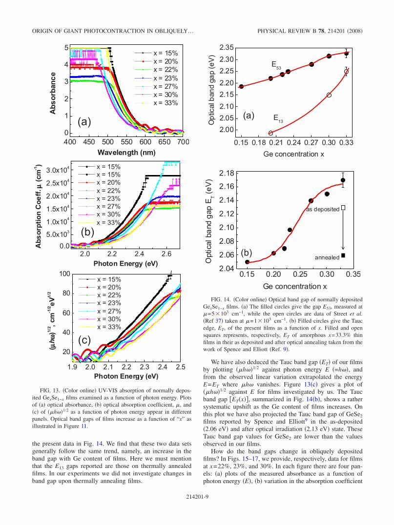
the present data in Fig. 14. We find that these two data setsgenerally follow the same trend, namely, an increase in theband gap with Ge content of films. Here we must mentionthat the E13 gaps reported are those on thermally annealedfilms. In our experiments we did not investigate changes inband gap upon thermally annealing films.
We have also deduced the Tauc band gap �ET� of our filmsby plotting ��h�1/2 against photon energy E �=h�, andfrom the observed linear variation extrapolated the energyE=ET where �h vanishes. Figure 13�c� gives a plot of��h�1/2 against E for films investigated by us. The Taucband gap �ET�x��, summarized in Fig. 14�b�, shows a rathersystematic upshift as the Ge content of films increases. Onthis plot we have also projected the Tauc band gap of GeSe2films reported by Spence and Elliott9 in the as-deposited�2.06 eV� and after optical irradiation �2.13 eV� state. TheseTauc band gap values for GeSe2 are lower than the valuesobserved in our films.
How do the band gaps change in obliquely depositedfilms? In Figs. 15–17, we provide, respectively, data for filmsat x=22%, 23%, and 30%. In each figure there are four pan-els: �a� plots of the measured absorbance as a function ofphoton energy �E�, �b� variation in the absorption coefficient
400 450 500 550 600 650 7000
1
2
3
4
5Absorbance
Wavelength (nm)
x = 15%x = 20%x = 22%x = 23%x = 27%x = 30%x = 33%
1.9 2.0 2.1 2.2 2.3 2.4 2.5
20
40
60
80
100x = 15%x = 20%x = 22%x = 23%x = 27%x = 30%x = 33%
( µµ µµh ωω ωω)1/2 ,cm
-1/2eV
1/2
Photon Energy (eV)
2.0 2.2 2.4 2.60.0
5.0x1031.0x1041.5x1042.0x1042.5x1043.0x104
AbsorptionCoeff.
µµ µµ(cm-1)
Photon Energy (eV)
x = 15%x = 15%x = 20%x = 22%x = 23%x = 27%x = 30%x = 33%
(a)
(b)
(c)
FIG. 13. �Color online� UV-VIS absorption of normally depos-ited GexSe1−x films examined as a function of photon energy. Plotsof �a� optical absorbance, �b� optical absorption coefficient, �, and�c� of ��h�1/2 as a function of photon energy appear in differentpanels. Optical band gaps of films increase as a function of “x” asillustrated in Figure 11.
0.15 0.18 0.21 0.24 0.27 0.30 0.33
2.002.052.102.152.202.252.302.35
E13
E53
Opticalbandgap(eV)
Ge concentration x
(a)
(b)
0.15 0.20 0.25 0.30 0.352.04
2.06
2.08
2.10
2.12
2.14
2.16
2.18
annealed
as depositedOpticalbandgapE T(eV)
Ge concentration x^
FIG. 14. �Color online� Optical band gap of normally depositedGexSe1−x films. �a� The filled circles give the gap E53, measured at�=5�103 cm−1, while the open circles are data of Street et al.�Ref 37� taken at �=1�103 cm−1. �b� Filled circles give the Taucedge, ET, of the present films as a function of x. Filled and opensquares represents, respectively, ET of amorphous x=33.3% thinfilms in their as deposited and after optical annealing taken from thework of Spence and Elliott �Ref. 9�.
ORIGIN OF GIANT PHOTOCONTRACTION IN OBLIQUELY… PHYSICAL REVIEW B 78, 214201 �2008�
214201-9

1.8 2.0 2.2 2.4 2.6 2.8 3.0
0.0
5.0x10³
1.0x10⁴
1.5x10⁴
2.0x10⁴
2.5x10⁴
0o
45o
60o
80o
Absorptioncoefficient
µ(cm-1)
Photon energy (eV)
(b)
(a)
X = 23%
X = 23%
400 450 500 550 600 650 7000
1
2
3
4
5
0o
45o
60o
80oAbsorbance
Wavelength (nm)
1.8 2.0 2.2 2.4 2.6 2.80
50
100
150
200
250
300
0o
45o
60o
80o
(µhω)1/2cm
-1/2eV
1/2
Photon energy (eV)
0 20 40 60 801.9
2.0
2.1
2.2
2.3
2.4
ET
E53
Opticalbandgap(eV)
Obliqueness angle (degree)
X = 23%
X = 23%
(c)
(d)
FIG. 16. �Color online� Plots of �a� UV-VIS absorbance and �b�absorption coefficient � of GexSe1−x thin films at x=23% as a func-tion of photon energy for films at indicated obliqueness angle �.Plots of �c� ��h�1/2 against E, and �d� variations in the opticalband gaps E53 and ET of x=23% films as a function of obliquenessangle.
(b)
(a)
X = 22%
X = 22%
1.8 2.0 2.2 2.4 2.6 2.8 3.0 3.20.0
5.0x1031.0x1041.5x1042.0x1042.5x1043.0x104
0o
45o
60o
80o
AbsorptionCoefficientµ(cm-1)
Photon energy (eV)
400 450 500 550 600 650 7000
1
2
3
4
0o
45o
60o
80o
Absorbance
Wavelength (nm)
0 20 40 60 802.00
2.05
2.10
2.15
2.20
2.25
ET
E53
Opticalbandgap(eV)
Obliqueness angle (degree)
(d)
(c)
X = 22%
1.8 2.0 2.2 2.4 2.6 2.8
50
100
150
200
250
0o
45o
60o
80o
(µhω)1/2cm
-1/2eV
1/2
Photon energy (eV)
X = 22%
FIG. 15. �Color online� Plots of �a� UV-VIS absorbance and �b�absorption coefficient � of GexSe1−x thin films at x=22% as a func-tion of photon energy for films at indicated obliqueness angle �.Plots of �c� ��h�1/2 against E, and �d� variations in the opticalband gaps E53 and ET of x=22% films as a function of obliquenessangle.
JIN et al. PHYSICAL REVIEW B 78, 214201 �2008�
214201-10

��E�, �c� plots of ��h�1/2 against E, and �d� variations inthe E53��� band gap and the ET��� Tauc band gap as func-tions of the angle �. A perusal of these data show that E53���band gaps generally increase with � but not monotonically.For compositions at x=22%, 23%, and 27%, the band gapsat first decrease as � increases from 0° to 40° or 60°, andthereafter one observes the gap to increase as � increases to80°. The threshold behavior nearly vanishes as x increases to30% �Fig. 17� and band gaps increase almost monotonicallywith �.
In Fig. 18 and Table I, we compare the E53��� band gapsof normally deposited ��=0� with obliquely deposited films��=80°�. We find that the band gaps of obliquely depositedfilms are significantly larger than of normally depositedfilms. At x=33.33%, the upshift in the energy gap is nearly0.38 eV, and it steadily decreases to nearly vanish as x de-creases to 15%. The result for films at x=33.33% is all themore interesting given that our Raman results reveal ob-liquely deposited GeSe2 films display a line-shape character-istic of a film of Ge25Se75 composition. There are clearlyother factors that come into play to understand these data,issues we discuss in Sec. IV.
4. IR reflectance
IR response of thin-film samples in the virgin and photo-contracted state were measured using a Thermo NicoletFTIR spectrometer model 870 using a variable angle reflec-tion attachment called Seagull marketed by Harrick Scien-tific Products, Inc. deuterated triglycine sulfate �DTGS� withpolyethylene or KBr window as detector, with KBr and solidsubstrate used as beam splitters, permitted the IR responsefrom the films to be recorded in the far- and mid-IR regions.The instrument is supported by OMNIC and Grams/AI soft-ware to acquire and analyze data. In a typical measurement,200 scans were programmed to yield 4 cm−1 resolution, andthe response over a wide frequency range from 200 to1200 cm−1 was recorded. We also recorded the IR responsefrom a GeO2 glass, and as expected observed vibrationalfeatures of tetrahedrally coordinated Ge to oxygen neighbors
(a)
X = 30%
X = 30%
400 500 600 700
0
1
2
3
4
5
0o
45o
60o
80oAbsorbance
Wavelength (nm)
X = 30%
(b)
2.0 2.5 3.00.0
5.0x1031.0x1041.5x1042.0x1042.5x1043.0x1043.5x104
0o
45o
60o
80o
Absorptioncoefficient(cm-1)
Photon energy (eV)
0 20 40 60 80
2.1
2.2
2.3
2.4
2.5
ET
E53
Opticalbandgap(eV)
Obliqueness angle (degree)
1.6 1.8 2.0 2.2 2.4 2.6 2.8 3.00
100
200
300
0o
45o
60o
80o
(µhω)1/2cm
-1/2eV
1/2
Photon energy (eV)
(c)
(d)
X = 30%
X = 30%
FIG. 17. �Color online� Plots of �a� UV-VIS absorbance and �b�absorption coefficient � of GexSe1−x thin films at x=30%, as afunction of photon energy for films at indicated obliqueness angle�. Plots of �c� ��h�1/2 against E, and �d� variations in the opticalband gaps E53 and ET of x=30% films as a function of obliquenessangle.
0.15 0.20 0.25 0.30 0.35
2.2
2.3
2.4
2.5
2.6
2.7
α = 80o
α = 0o
OpticalbandgapE 5
3(eV)
Ge concentration x
FIG. 18. �Color online� Optical band gap E53 of normally andobliquely deposited GexSe1−x thin films as a function of “x.” Notethe much higher value of the gap in obliquely deposited films.
ORIGIN OF GIANT PHOTOCONTRACTION IN OBLIQUELY… PHYSICAL REVIEW B 78, 214201 �2008�
214201-11

near 900 cm−1, as illustrated in Figs. 19�a� and 19�b�. Weconfirm that films become partially oxidized if the cold stageis not thoroughly purged with N2 gas during irradiation fromthe Hg-Xe lamp. We illustrate the finding in Fig. 19�b�,
which compares the IR response of a film at x=23%, bothbefore and after irradiation. On the other hand, in the pres-ence of a N2 gas flow, we found no evidence of oxidation fora film at x=22%, as illustrated in Fig. 19�a�. Thus, we be-lieve that the observed trends in PC, band-gap variation, andRaman scattering reported here on amorphous Ge-Se thinfilms represent the intrinsic behavior of these films, and arenot related to any surface oxidation effects.9
IV. DISCUSSION
In thin-film deposition, chemical stoichiometry of depos-ited films can differ from those of the evaporation charge,particularly if elements �Ge, Se� of widely different meltingtemperatures are being evaporated, as in the present case. Toascertain stoichiometries of deposited films we used Ramanscattering as a quantitative probe. The approach workslargely because Raman scattering of binary GexSe1−x filmsand glasses, in the 0�x�1 /3 range, possess reasonablysharp modes, which systematically blueshift and change inscattering strength as the chemical stoichiometry x of glassesor films increases. Raman scattering on binary GexSe1−xglasses taken at every 2 atomic % of Ge concentration inter-val in the 15%�x�34% range have been studiedextensively.12,20,26,37 Observed line shapes were least-squaresfit to a superposition of requisite number of Gaussians, modefrequencies and mode scattering strengths of the A1 mode, A1
c
mode, and Sen chain mode were obtained, and these resultsare summarized in Fig. 11 as mentioned earlier. A perusal ofthe line-shape parameters of the normally deposited ��=0°�films at all compositions x suggest that their chemical sto-ichiometries are quite close to those of corresponding bulkglasses used as evaporation charges. Film stoichiometries areestablished from frequency of the A1 and A1
c vibrationalmodes and their scattering strengths. For example, for a nor-mally deposited film at x=1 /3, the A1 mode frequency isfound to be 199.3�6� cm−1. The mode frequency, when pro-jected on the plot of Fig. 11�a�, yields a stoichiometry of x=32.8%. That inference on film stoichiometry is indepen-dently corroborated by the frequency of the A1
c mode near217 cm−1 �Fig. 11�b��. On the other hand for the obliquelydeposited �=80° films at x=33.3%, �Fig. 10� Raman line-shape parameters suggest a film stoichiometry and molecularstructure characteristic of a bulk glass at x�25%. Parallelconsiderations at other film compositions have likewise per-
TABLE I. Tauc edge �ET�, and gap at an absorption coefficient of 5�103 cm−1 �E53� of GeSe2 thin films.Typical error on these measurements is 0.04 eV.
GeSe2 thin filmsET�E53� of films in eVof as deposited films
ET of films in eVafter illumination
0° �present work, New Delhi� 2.17 �2.33�0° �present work, Sofia� 2.04 �2.40�0° �Spence & Elliott� 2.06a 2.13
80° �present work, New Delhi� 2.05 �2.68� 2.04 �2.67�80° �Spence & Elliott� 1.84a 1.69
aOnly ET is available for these samples.
1200 1000 800 600 400
Ge23Se77 filmbefore irradiation
Ge23Se77 filmafter irradiation
g-GeO2
IRAbsorbance(Arb.Units)
wavenumber (cm-1)
Ge22Se78 filmbefore irradiation
Ge22Se78 filmafter irradiation
g-GeO2
IRAbsorbance(Arb.Units)
1200 1000 800 600 400
wavenumber (cm-1)
(a)
(b)
FIG. 19. �Color online� IR absorbance of �a� GeO2 glass andamorphous Ge22Se78 films before and after irradiation, and �b�GeO2 glass and amorphous Ge23Se77 films before and after irradia-tion. In �a� the cold stage was thoroughly flushed with N2 gas whilein �b� this was not the case. Note the presence of oxidation in the23% film in �b� but the absence of it in the 22% film in �a�.
JIN et al. PHYSICAL REVIEW B 78, 214201 �2008�
214201-12

mitted decoding stoichiometry, as well as the molecularstructure of films.
A. Nanoscale phase separation of obliquely deposited GexSe1−x
thin films
The Raman scattering of obliquely ��=80°� depositedGeSe2 films reveal line shapes that show a close similarity toa glass of GeSe3 stoichiometry �Figs. 7 and 10�. On the otherhand the band gap of such films �2.68 eV� is considerablylarger than the gap of GeSe3 glass �2.38 eV�. How are we toreconcile these results? We would like to suggest that thesefilms are intrinsically segregated on a nanoscale into twodistinct phases: one of these �A� consists of columns ofnearly GeSe3 stoichiometry and the other phase �B� is ofnearly Ge2Se3 stoichiometry. We believe such nanoscalephase separation is largely driven by network strain consid-erations: nanophase A possesses an optimal connectivity andit spontaneously grows as a stress-free structure. NanophaseB is over connected and thus strained, and it fills the inter-columnar void regions. Nanophase A is Se richer than thebase material �GeSe2� while nanophase B is Se-poorer thanthe base material. One may describe the underlying nano-scale phase separation on grounds of chemical stoichiometryas follows:
Ge1/3Se2/3 = �4
9�Ge1/4Se3/4�A phase�
+ �5
9�Ge2/5Se3/5�B phase� . �2�
The first term on the right-hand side of Eq. �2� represents theSe-rich A nanophase while the second term the Ge-rich Bnanophase. Equation �2� suggests that the concentration ofthese two nanophases must be comparable �4:5�. In practiceRaman scattering is dominated by the A nanophase becauseits band gap is close to that of the 647-nm �1.96-eV� excitingradiation. Indeed, one can account for the observed lineshape in terms of contributions of these two nanophases asshown in Fig. 20. The line shapes of the two nanophases aretaken from those of corresponding bulk glasses. Films at x=23% reveal Raman line shapes that are independent of theobliqueness angle. Oblique films at this privileged composi-tion consist only of the A nanophase present as columns.Raman line-shape parameters, �CS���, �CS���, andAES /ACS���, of films at x=23% place the stoichiometry ofthe nanophase A close to GeSe3. These Raman line-shapeparameters in bulk GexSe1−x glasses have been established inthe 15%�x�40% range at every 2 at.% interval �Fig. 11�.The present data on films shown in Fig. 10 can, thus, beanalyzed to provide details of film molecular structure. Itappears that nanophase A can exist in either a 3D morphol-ogy as in a bulk glass �Fig. 11� or in quasi-1D columns as inthin films deposited at high obliqueness angle �=80° films�Fig. 9�.
Our Raman data suggest a totally different picture for thinfilms deposited at low x, i.e., x=23% and 20%. In Fig. 10,we show a plot of the three parameters, �CS���, �CS���, andIES / ICS��� for films at x=20% and 23%, and these param-
eters remain largely independent of obliqueness angle. Theseline-shape parameters serve to define the network backboneand suggest that the chemical stoichiometry of films remainsindependent of �. Even when columns appear at high ob-liqueness angle ��=80°�, their stoichiometry is close to thatof bulk glass used as the starting material.
For the Se-rich film at x=15%, a perusal of the data ofFig. 10 shows that the three parameters, �CS���, �CS���, andIES / ICS���, are all larger than those for films at x=20% and23%. In particular, the mode frequencies of CS and ES tet-rahedral units are present in a local environment that is quitesimilar to that of a bulk glass near x=25%. These data sug-gest that films at x=15% are also intrinsicallyheterogeneous—composed of Ge-rich regions and Se-rich re-gions. The three parameters above serve to define how Geatoms bond in films. On the other hand, information on theSe-rich phase comes more reliably from an analysis of theSen chain mode frequency, and particularly the ratio R of thescattering strength of the broad Sen mode relative to the CSmode. Our Raman results reveal the ratio R to increase from1.1 at �=0° to 1.7 at �=80°. These data suggest that at lowobliqueness angles films are intrinsically segregated, while athigh obliqueness angles, as columns appear, they are repre-sentative of a network with a stoichiometry of about x=15%.
Molecular structure results on films suggested from theRaman data can be briefly summarized. Films at x�25% areintrinsically segregated on a nanoscale into two phases A andB, with the A phase representing the column material and theB phase the intercolumnar material. Films at x=20% and23% are intrinsically homogeneous, i.e., there is no evidenceof a variation in stoichiometry with �. On the other hand,film at x=15% appears to be again segregated into Ge-richand Se-rich regions, and such segregation almost vanishes as� increases to 80°.
B. Band-gap variation with oblique deposition and carrierlocalization
Earlier reports by Street et al.38 and P. Nagels et al.,31
established that the optical gap of normally deposited
100 150 200 250 300 350
Ge36Se64 Ge25Se75
Sen chainES
CS
Intensity(Arb.Units)
Raman Shift (cm-1)
FIG. 20. �Color online� Simulation of the observed Raman lineshape of an obliquely ��=80� deposited GeSe2 film in terms of twocontributions, one of Ge25Se75 bulk glass �A nanophase� and theother of Ge36Se64 bulk glass �B nanophase�, revealing nanoscalephase separation of such films. See Eq. �2� in text.
ORIGIN OF GIANT PHOTOCONTRACTION IN OBLIQUELY… PHYSICAL REVIEW B 78, 214201 �2008�
214201-13

GexSe1−x thin films increases with Ge concentration �Fig.14�. Our results confirm the finding and reveal optical gapsof films to be larger than those reported earlier at the samefilm stoichiometry x. In the present work, films in most caseswere relaxed at room temperature for over a year beforeexamination. Raman data on normally deposited films arefound to be quite similar to those of the bulk glasses used asstarting materials to evaporate them. These data suggest thatour films are homogeneous and relaxed, and the larger bandgap most likely a consequence of these circumstances.
The optical band gap of our thin films examined as afunction of obliqueness angle � displays interesting trends.For film compositions close to the threshold value, x�22%,band gaps are found �Fig. 15�d�� to first decrease with �, toshow a broad and shallow minimum in the 45° ���60°range, and to increase thereafter to show a maximum at highobliqueness angle, �=80°. The behavior is also observed atx=23% �Fig. 16�d��. But as x increases to 30%, the broadand shallow minimum in the band gap becomes less con-spicuous, and a general increase in the band gap is observedwith � �Fig. 17�d��. In Fig. 15, we compare the optical gap ofour normally deposited films ��=0� with those of obliquelydeposited ��=80� ones as a function of film stoichiometry x.The results show that both gaps increase with x; however, theincrease in the gap of obliquely deposited films, particularlyat x�23%, is significantly larger than of normally depositedfilms. In particular, E53 band gap of �=80 films �2.68 eV��Fig. 18� is found to be much larger than the gap of normallydeposited ��=0� films �2.30 eV�.
The dielectric constant �� of GeSe2 glass was establishedfrom IR reflectance measurements39 and found to have avalue of =12.31. If one assumes the electron effectivemass, m�, in these films to be 0.1 m, a value typical of manycompound semiconductors,40 we estimate the exciton radiusR in amorphous GeSe2 films to be
R = a0�m�
m� = 6.3 nm. �3�
In Eq. �3�, ao represents the first Bohr radius of 0.051 nm andm the rest mass of an electron. The blueshift of the E53 op-tical gap we would suggest represents localization of carriersin the columns. This can only happen if the columns are ofnanoscale dimensions, i.e., of the order of R�10 nm or so.We are, thus, led to the notion that carriers must be localizedin nanometric-sized atomic filaments of GeSe3. These atomicfilaments of GeSe3 are probably made up of chains of corner-sharing �GeSe1/2�4 tetrahedra that are bridged by edge-sharing Ge�Se1/2�4 ones, the structural motif found in thecrystal structures of the high-temperature form of GeSe2 andthe metastable crystalline phase of Ge4Se9.41 The columnsobserved in SEM investigations �Figs. 4–6� of about 50-nmdiameter in lateral dimension must then be viewed asbundles36 of nanometric-sized atomic filaments, and the0.38-eV blueshift in band gap of such films is the result ofconfinement of electron-hole pairs in such nanofilaments.The data of Fig. 18 reveals that such a carrier confinementeffect is present in films at x�25%, and that the effect in-creases monotonically as x increases to 33.3%. Carrier local-ization effect in nanophase A is accentuated by the presence
of B nanophase. The latter grows as x increases and it servesto laterally confine of the nanofilaments �A�. One can thenthink of an obliquely deposited �=80° film at x=33.3% ascomposed of multilayers of alternating GeSe3 nanofilaments�A� and Ge40Se60 layers �B� growing at an angle ��70° �seeEq. �1��. To summarize, the large increase in band gap ofobliquely deposited films in relation to normally depositedones, we believe, results from carrier localization effects innanofilaments that form bundles and are observed as col-umns in SEM images. We believe that the chemistry of thecolumns remains close to GeSe3 in all films at high x��25%�. A glass network of GeSe3 stoichiometry will residein the IP of the Ge-Se binary and would form stress-freestructures.
C. Optimization of the giant photo contraction (GPC) effect inthe intermediate phase
It is widely known that porous thin films of many mate-rials including Si can be grown by oblique deposition. Butonly a select few of these obliquely deposited films undergoa thickness contraction when illuminated by pair-producingradiation.36 In the case of Si, for example, little or no photo-contraction is observed.8 Thus, there are factors other thancolumnar growth that must come into play to account for theselective nature of the PC effect. The optimization of thegiant photo contraction �GPC� effect in the IP of the Ge-Sebinary �Fig. 3� provides an important clue in understandingthe molecular origin of the effect.
In the binary GexSe1−x system, it has recently beenshown26 from Raman scattering experiments performed as afunction of externally applied hydrostatic pressure that glasscompositions in the IP form networks that are stress free. Inthese experiments on bulk glasses, one has found the exis-tence of a threshold pressure,37 Pc, that must be exceeded bythe applied pressure P for the Raman active vibrational modeof corner-sharing GeSe4 tetrahedra �near 200 cm−1� to blue-shift. The threshold pressure, Pc�x�, serves as a measure ofnetwork stress. It must be exceeded by the applied pressurefor the network to be compressed and sense the appliedstress. Interestingly, these experiments show that the compo-sitional variation in Pc�x� closely tracks that of the nonre-versing enthalpy term �Hnr�x� of the glass transition.26 Glasscompositions in the IP �20%�x�25%� display a vanishingPc and �Hnr, and both these terms change remarkably as onegoes away from the IP, both above �x�25%� and below�x�20%� the IP. The vanishing of Pc in the IP is a remark-able finding. The vanishing of Pc is a result characteristic ofa crystalline solid, i.e., a network that is at equilibrium.These data underscore that glass compositions in the IP formnetworks that are stress free and in a state of quasiequilib-rium.
The second set of experiments of relevance here bear onthe giant photoacoustic softening observed in binaryGexSe1−x glasses in Brillouin scattering measurements19
when their composition x is close to 20%, the mean-fieldrigidity transition. The exciting radiation in these Brillouinexperiments �647-nm radiation from a Kr-ion laser� appar-ently strongly couples to the network when it is stress free. A
JIN et al. PHYSICAL REVIEW B 78, 214201 �2008�
214201-14

parallel behavior is encountered in Raman scattering whenthe power density of the exciting radiation �647 nm� is sub-stantially increased,12 and one finds the IP structure to col-lapse to its centroid near x=23%. The photoacoustic soften-ing in Brillouin experiments and the photomelting of the IPin Raman scattering experiments, both performed as a func-tion of laser power density, have at their base the same cen-tral idea. Near band-gap light leads to facile photomelting27
of stress-free disordered networks but not of stressed ones�see below�.
The optimization of the GPC effect in films residing in theIP can now be commented upon. We can gauge stress inevaporated films by looking at the widths of Raman vibra-tional modes. A perusal of these data reveals that atx=23%, full width at half maximum of the ES mode in ob-liquely deposited thin films �tf� ��=80°� is �ES
tf
=10.75�50� cm−1, nearly the same as in the bulk glasses�bg�, �ES
bg =10.75�50� cm−1. At x=30%, we find �EStf
=11.50�50� cm−1 to be greater than �ESbg =9.70�50� cm−1. At
x=33.3%, we find �EStf =16.00�50� cm−1 again to be greater
than �ESbg =9.70�50� cm−1. At x=15%, we find �ES
tf
=18.00�50� cm−1 to be substantially greater than �ESbg
=10.30�50� cm−1. These data reveal that the deposited filmsat compositions both above and below the IP are inhomoge-neously stressed while those in the IP are not.
Near the composition x=23%, we have a 3D network inthe normally deposited ��=0°� film but a quasi-1D columnarstructure in the obliquely deposited ��=80°� films. In thelatter case, films are porous, and the porosity derives fromthe free volume present between columns. Our Raman scat-tering results show that the molecular structure of these filmsis independent of �. In both instances ��=0° and 80°� wehave networks formed in such films that are intrinsicallystress free. When oblique films are exposed to radiation fromHg-Xe lamp, photomelting of the columns occurs, i.e., thecolumns collapse and lead to a change in film thickness asthe films densify.
The underlying photostructural transformations can be de-scribed as follows. The minuscule nonreversing enthalpy atTg �Fig. 3� for networks in the IP suggests that such networkspossess high configurational entropies that are close to liquidentropies. Just the reverse is the case for networks residingoutside the IP, which possess an order of magnitude largernonreversing enthalpy of melting at Tg, and must sit at thebottom on an entropy landscape. The role of pair-producingradiation is to create electron-hole pairs, leading to excitons,which eventually recombine delivering band gap worth ofenergy �2 eV� to covalent bonds locally, permitting them toswitch by a process that has been described by Fritzsche.27
With increasing flux of UV radiation, switching of bondsbecomes pervasive and leads to facile light-induced meltingof networks in the IP since in their pristine state �absence oflight� they almost have liquidlike entropies. On the otherhand, networks residing outside the IP, which possess a muchlarger nonreversing heat flow, have a larger entropic barrierto overcome before the photomelted state can be realized.These ideas provide a physical basis to understand how pair-producing radiation interacts so differently with stress-freenetworks than with stressed ones.
At higher x, such as at x=30% and 33.3 %, oblique filmswith nanoscale phase separate into columns of GeSe3 stoichi-
ometry �phase A� with the Ge40Se60 phase �B� filling poresbetween columns.18 Here the stress-free A phase is photoac-tive phase, while the stressed B phase is photoinactive. ThePC effect in oblique films ��=80°� steadily decreases as xincreases above 27% because of the presence of the photo-inactive B phase filling the pores. Some reconstruction of theA with B nanophase occurs upon photo-illumination as pho-tomelting proceeds, precluding a complete collapse of col-umns that would have occurred if the B nanophase wereabsent. The evidence of A and B nanophases reconstructingupon PC comes from our Raman scattering data examined asa function of depth �Fig. 12�. There are two sets of spectrashown as a function of depth “d” using a confocal micro-scope. Here d refers to a depth of about 0.2 �m and corre-sponds to a complete rotation of the knob affecting a z dis-placement of the focal point of the objective. Note that at adepth of 2d the Sen chain mode near 260 cm−1 decreases instrength as the strength of the ES mode near 217 cm−1 in-creases. We visualize these changes as representing theGe25Se75 A phase reconstructing with the Ge40Se60nanophase B to form a GeSe2-like network. The underlyingprocess is the same as given by Eq. �2� except now the re-action proceeds from right to left, partially undoing the de-mixing that occurred during oblique deposition of films.These considerations provide a sound basis to understand thereduction of the PC at x�25% �Fig. 3�.
Why does the PC effect steadily decrease in oblique filmsat x�20%? We have already noted that Raman scattering offilms at x�23% display vibrational features �Figs. 9 and 10�that are largely independent of the obliqueness angle. Inother words, the chemical stoichiometry of columns formedin oblique films at x�23% must be the same as that of the3D networks formed in normally deposited films. Incorpora-tion of excess Se in the optimally connected GeSe3 columnsrenders them progressively stressed. The stressed characterof networks in the flexible phase was independently estab-lished from the pressure Raman experiments alludedearlier.42 Radiation from the Xe-Hg lamp now no longercouples well to glass networks in the flexible phase as it didwhen columns were stress free at x=23%. Photomelting ofthe columns is now suppressed with the result that the PCeffect almost vanishes at x=15% �Fig. 3�. These consider-ations on the contrasting role of light interaction withstressed and stress-free networks provides a basis to under-standing why the PC effect is optimized in the IP.
D. Optical absorption changes upon illumination of obliquelydeposited GexSe1−x thin films
In our experiments we did not investigate optical absorp-tion shifts in obliquely deposited films as a function of lightirradiation. Such a study was however reported earlier bySpence and Elliott,9 and Rajgopalan et al.43 For films irradi-ated in vacuum, these workers found normally depositedfilms ��=0°� to photobleach, while obliquely deposited ones��=80°� to photodarken. Given our findings of a change inthe optical band gap with obliqueness angle �Figs. 15 and17�, a rather straightforward interpretation can be advancedto understand the switch from photobleaching to photodark-
ORIGIN OF GIANT PHOTOCONTRACTION IN OBLIQUELY… PHYSICAL REVIEW B 78, 214201 �2008�
214201-15

ening as a function of obliqueness angle �. Freshly depositedfilms are usually stressed, and these can be relaxed either bya thermal anneal or by illumination to near-band-gap radia-tion. For Ge-Se films, the optical band edge usually shifts upas stress is released, leading to a photobleaching. Films de-posited at high obliqueness angles usually have a larger bandgap as found in the present work. Upon illumination to vis-ible light one can expect columns to collapse, and the under-lying enhancement of the optical gap due to carrier confine-ment effects to be lost. The natural consequence will be alowering of the band gap, i.e., photodarkening. These stress-related effects are not expected to be strongly influenced bysurface oxidation of films since these are still largely bulkrather than surface effects.9
The present findings on the origin of PC in obliquely de-posited films of the Ge-Se binary can be formalized into ageneral prediction. One expects the PC effect to be optimizedfor obliquely deposited thin films when their chemical sto-ichiometry resides in the IP of corresponding bulk glasses.IPs in several families of binary and ternary chalcogenideglass systems have now been identified.25 For example, inthe Ge-As-Se ternary system, a fairly large domain of com-positions resides in the IP.44 In some early work reported onthis ternary glass system, one of the largest PC effect �26%�was observed32 for the Ge0.20Se0.75As0.05 composition. Thisparticular composition corresponds to a mean coordinationnumber r=2.45 if one takes Ge, As, and Se to be fourfold,threefold, and twofold coordinated. The composition residesin the IP �Ref. 44� of the Ge-As-Se ternary. We predict that agiant PC effect will also be observed in the ternary Ge-P-Se,binary As-Se, and binary P-Se over a wide range of compo-sitions encompassing the IP.
V. SUMMARY
Obliquely deposited GexSe1−x thin films at several com-positions in the 15%�x�33.3% range and at obliquenessangles in the 0���80° range at each x were evaporated onSi and glass substrates. Raman scattering, IR reflectance, andoptical absorption measurements were undertaken to charac-terize the vibrational density of states and optical band gapof films. Edge views of the films in SEM confirm the colum-nar structure of the obliquely deposited films.29 Filmsmounted in a cold stage flushed with N2 gas were irradiatedto Hg-Xe arc lamp and confirmed oblique films ��=80°� toundergo photocontraction �PC�. IR reflectance measurements
confirm the absence of photo-oxidation in our films. Filmthickness reduction upon illumination was measured with adiamond stylus profilometer. Trends in PC exhibit a bell-shaped curve with a rather large effect localized in the inter-mediate phase, 20%�x�25%, of the present binary bulkglass system. The columns observed in SEM investigationsreveal a high aspect ratio with length and lateral width of1.5 �m and about 50 nm in diameter. The blueshift �up to0.38 eV� in band gap of oblique films ��=80°� in relation tonormally deposited ��=0°� films, we trace to confinement ofelectron-hole pairs produced upon optical absorption innanofilaments. We view the columns formed in films to becomposites or bundles of nanometric-sized atomic filaments,and trace the giant PC effect in the IP to the stress-free char-acter of filaments of Ge25Se75 stoichiometry that undergo fac-ile photomelting, resulting in their collapse and the conse-quent densification of films. The underlying photostructuraleffect involves a rapid switching of Ge-Se and Se-Se cova-lent bonds mediated by a recombination of geminate exci-tons following absorption of pair-producing radiation. Pho-tomelting of corresponding bulk compositions that belong tothe IP has been demonstrated separately.20 Raman scatteringsuggests that Ge-rich films �25%�x�33.3%� intrinsicallysegregate on a nanoscale into Ge25Se75-based nanometriccomposite filaments and a compensating Ge-rich phase �ap-prox. Ge40Se60 stoichiometry� that progressively fills the in-tercolumnar free space. And the steady loss of PC with in-creasing x is traced to the growth of the Ge-rich phase, whichis stressed and thus photoinactive. In contrast, Raman scat-tering data show Se-rich films �x�20%� to be homogeneous,and we identify the loss of PC to the accumulation of net-work stress in such Se-rich columns, which renders themprogressively photoinactive. Evidence of accumulation ofnetwork stress in Se-rich bulk glasses was demonstrated inpressure Raman experiments earlier. In summary, the com-prehensive set of measurements on a Ge-Se thin films pro-vide the microscopic origin of the giant PC effects in thinfilms of the chalcogenides. These findings provide a goodbasis to predict trends in PC on other chalcogenide glasssystems where the IP has been established.24
ACKNOWLEDGMENTS
We acknowledge discussions with Bernard Goodman, Pe-ter Smirniotis, and Maria Mitkova during the course of thiswork. This work was supported by the NSF through GrantNo. DMR 04-56472.
1 M. N. Kozicki and M. Mitkova, in Nanotechnology, InformationTechnology Vol. 3, edited by R. Waser �Wiley, New York, 2008�,p. 485.
2 M. Kincl and L. Tichy, Mater. Chem. Phys. 103, 78 �2007�.3 P. Krecmer, A. M. Moulin, R. J. Stephenson, T. Rayment, M. E.
Welland, and S. R. Elliot, Science 277, 1799 �1997�.4 B. Singh, S. Rajagopalan, P. K. Bhat, D. K. Pandya, and K. L.
Chopra, J. Non-Cryst. Solids 35-36, 1053 �1980�.
5 B. Singh, S. Rajagopalan, and K. L. Chopra, J. Appl. Phys. 51,1768 �1980�.
6 B. Singh, S. Rajagopalan, P. K. Bhat, D. K. Pandya, and K. L.Chopra, Solid State Commun. 29, 167 �1979�.
7 A. G. Dirks and H. J. Leamy, Thin Solid Films 47, 219 �1977�.8 J. C. Knights, J. Non-Cryst. Solids 35-36, 159 �1980�.9 C. A. Spence and S. R. Elliott, Phys. Rev. B 39, 5452 �1989�.
10 E. Marquez, A. M. Bernal-Oliva, J. M. Gonzalez-Leal, R. Prieto-
JIN et al. PHYSICAL REVIEW B 78, 214201 �2008�
214201-16

Alcón, and R. Jiménez-Garay, J. Non-Cryst. Solids 222, 250�1997�.
11 K. Starbova, J. Dikova, and N. Starbov, J. Non-Cryst. Solids210, 261 �1997�.
12 X. W. Feng, W. J. Bresser, and P. Boolchand, Phys. Rev. Lett.78, 4422 �1997�.
13 D. Selvanathan, W. J. Bresser, and P. Boolchand, Phys. Rev. B61, 15061 �2000�.
14 S. Chakravarty, D. G. Georgiev, P. Boolchand, and M. Micou-laut, J. Phys.: Condens. Matter 17, L1 �2005�.
15 P. Boolchand, D. G. Georgiev, and B. Goodman, J. Optoelectron.Adv. Mater. 3, 703 �2001�.
16 P. Boolchand, G. Lucovsky, J. C. Phillips, and M. F. Thorpe,Philos. Mag. 85, 3823 �2005�.
17 D. G. Georgiev, M. Mitkova, P. Boolchand, G. Brunklaus, H.Eckert, and M. Micoulaut, Phys. Rev. B 64, 134204 �2001�.
18 P. Boolchand, M. Jin, D. I. Novita, and S. Chakravarty, J. RamanSpectrosc. 38, 660 �2007�.
19 J. Gump, I. Finkler, H. Xia, R. Sooryakumar, W. J. Bresser, andP. Boolchand, Phys. Rev. Lett. 92, 245501 �2004�.
20 P. Boolchand, X. Feng, and W. J. Bresser, J. Non-Cryst. Solids293-295, 348 �2001�.
21 J. C. Phillips, J. Non-Cryst. Solids 34, 153 �1979�.22 M. F. Thorpe, J. Non-Cryst. Solids 57, 355 �1983�.23 M. F. Thorpe, D. J. Jacobs, M. V. Chubynsky, and J. C. Phillips,
J. Non-Cryst. Solids 266-269, 859 �2000�.24 P. Boolchand, M. Micoulaut, and P. Chen, in Phase Change Ma-
terials: Science and Applications, edited by S. Raoux and M.Wuttig �Springer, Heidelberg, 2008�, p. 37.
25 P. Boolchand, P. Chen, and U. Vempati �unpublished�.26 F. Wang, S. Mamedov, P. Boolchand, B. Goodman, and M.
Chandrasekhar, Phys. Rev. B 71, 174201 �2005�.27 F. Fritzsche, in Insulating and Semiconducting Glasses, edited
by P. Boolchand �World Scientific, River-Edge, NJ, 2000�.
28 M. F. Thorpe, APS News 12 �2�, 10 �2003�.29 S. Rajagopalan, B. Singh, P. K. Bhat, D. K. Pandya, and K. L.
Chopra, J. Appl. Phys. 50, 489 �1979�.30 K. L. Chopra, Thin Film Phenomena �Krieger, New York, 1979�.31 P. Nagels, R. Mertens, and L. Tichy, in Properties and Applica-
tions of Amorphous Materials, edited by M. F. Thorpe and L.Tichy �Kluwer, Dordrecht, 2001�, p. 25.
32 K. L. Chopra, K. S. Harshvardhan, S. Rajagopalan, and L. K.Malhotra, Solid State Commun. 40, 387 �1981�.
33 K. Starbova, J. Dikova, V. Mankov, and N. Starbov, Vacuum 47,1487 �1996�.
34 K. Starbova, V. Mankov, J. Dikova, and N. Starbov, Vacuum 53,441 �1999�.
35 M. Levichkova, V. Mankov, N. Starbov, D. Karashanova, B.Mednikarov, and K. Starbova, Surf. Coat. Technol. 141, 70�2001�.
36 J. C. Phillips and M. L. Cohen, Phys. Rev. B 26, 3510 �1982�.37 K. Murase, in Insulating and Semiconducting Glasses, edited by
P. Boolchand �World Scientific, River Edge, NJ, 2000�.38 R. A. Street, R. J. Nemanich, and G. A. N. Connell, Phys. Rev. B
18, 6915 �1978�.39 M. Jin, M.S. thesis, University of Cincinnati, 2008.40 G. Burns, Solid State Physics �Academic, New York, 1985�, p.
243.41 H. Fjellvag, K. O. Kongshaug, and S. Stolen, J. Chem. Soc.
Dalton Trans. 2001, 1043.42 P. Boolchand, D. G. Georgiev, T. Qu, F. Wang, L. Cai, and S.
Chakravarty, C. R. Chim. 5, 713 �2002�.43 S. Rajagopalan, K. S. Harshavardhan, L. K. Malhotra, and K. L.
Chopra, J. Non-Cryst. Solids 50, 29 �1982�.44 T. Qu, D. G. Georgiev, P. Boolchand, and M. Micoulaut, Super-
cooled Liquids, Glass Transition and Bulk Metallic Glasses,MRS Symposia Proceedings No. 754 �Materials Research Soci-ety, Pittsburgh, 2003�, p. 111.
ORIGIN OF GIANT PHOTOCONTRACTION IN OBLIQUELY… PHYSICAL REVIEW B 78, 214201 �2008�
214201-17