optoelectronic analysis of multijunction wire array …...optoelectronic analysis of multijunction...
TRANSCRIPT
Optoelectronic analysis of multijunction wire array solar cellsDaniel B. Turner-Evans, Christopher T. Chen, Hal Emmer, William E. McMahon, and Harry A. Atwater Citation: J. Appl. Phys. 114, 014501 (2013); doi: 10.1063/1.4812397 View online: http://dx.doi.org/10.1063/1.4812397 View Table of Contents: http://jap.aip.org/resource/1/JAPIAU/v114/i1 Published by the AIP Publishing LLC. Additional information on J. Appl. Phys.Journal Homepage: http://jap.aip.org/ Journal Information: http://jap.aip.org/about/about_the_journal Top downloads: http://jap.aip.org/features/most_downloaded Information for Authors: http://jap.aip.org/authors
Downloaded 02 Jul 2013 to 131.215.220.166. This article is copyrighted as indicated in the abstract. Reuse of AIP content is subject to the terms at: http://jap.aip.org/about/rights_and_permissions

Optoelectronic analysis of multijunction wire array solar cells
Daniel B. Turner-Evans,1,a) Christopher T. Chen,1 Hal Emmer,1 William E. McMahon,2
and Harry A. Atwater11Thomas J. Watson Laboratories of Applied Physics, California Institute of Technology, Pasadena,California 91125, USA2National Renewable Energy Laboratory, Golden, Colorado 80401, USA
(Received 25 April 2013; accepted 10 June 2013; published online 2 July 2013)
Wire arrays have demonstrated promising photovoltaic performance as single junction solar cells
and are well suited to defect mitigation in heteroepitaxy. These attributes can combine in tandem
wire array solar cells, potentially leading to high efficiencies. Here, we demonstrate initial growths
of GaAs on Si0.9Ge0.1 structures and investigate III-V on Si1-xGex device design with an analytical
model and optoelectronic simulations. We consider Si0.1Ge0.9 wires coated with a GaAs0.9P0.1 shell
in three different geometries: conformal, hemispherical, and spherical. The analytical model
indicates that efficiencies approaching 34% are achievable with high quality materials. Full field
electromagnetic simulations serve to elucidate the optical loss mechanisms and demonstrate light
guiding into the wire core. Simulated current-voltage curves under solar illumination reveal
the impact of a varying GaAs0.9P0.1 minority carrier lifetime. Finally, defective regions at the
hetero-interface are shown to have a negligible effect on device performance if highly doped so as
to serve as a back surface field. Overall, the growths and the model demonstrate the feasibility of
the proposed geometries and can be used to guide tandem wire array solar cell designs.VC 2013 AIP Publishing LLC. [http://dx.doi.org/10.1063/1.4812397]
I. INTRODUCTION
A. Background
Wire array solar cells have the potential to significantly
reduce overall installed module costs by providing a light-
weight, flexible architecture that can be readily mounted on
rooftops and by using less material than conventional cell
designs while achieving comparable efficiencies. Towards this
end, single junction Si, CdS, InP, or GaAs wire array solar
cells have been synthesized and have demonstrated respectable
photovoltaic performance.1–12 Furthermore, Si wire array cells,
though grown on a rigid, expensive substrate, can be embed-
ded in a flexible polymer and peeled off, allowing the substrate
to be reused for further growths.13,14 The peeled off arrays still
absorb up to 96% of the incident light despite using 100 times
less material than a comparable planar Si cell.2 Si wire array
devices have reached efficiencies of 2-3% in liquid electro-
lyte15 and of up to 8% in large-area wire array solar cells,4 and
single wire measurements reveal that large area array efficien-
cies of greater than 17% are possible.3 Finally, InP nanowire
array cells have recently demonstrated a light conversion effi-
ciency of 13.8%.12 Thus, high performance single junction
wire array cells are rapidly becoming a proven technology.
B. Multijunction material selection
Multijunction arrays offer the advantages of wire array
solar cells along with both higher efficiencies and higher vol-
tages. The latter is especially attractive for photoelectro-
chemical solar fuel cells where the minimum voltage
required for water splitting exceeds 1.23 V. Along these
lines, GaP/Si wire heterostructures have been fabricated as
potential solar fuel devices.16 However, in order to obtain
high efficiencies for solar electricity generation, different
constituent materials must be selected; the limiting efficiency
for a GaP/Si combination is less than that of a single junction
Si cell alone due to severe current limiting by the GaP sub-
cell. Thus, to achieve a high efficiency device, the bandgaps
of the constituent materials must be chosen so that the photo-
current in each layer is matched. Additionally, mismatch
strain relieving dislocations can act as recombination centers
and thus lattice-matched material systems are desirable,
though recent work suggests that the wire geometry may
facilitate high quality growth of lattice mismatched materi-
als.17 When growing epitaxial layers on wires, dislocations
due to lattice mismatch can be forced to propagate radially
outward from the wire interface, allowing high quality mate-
rial to be grown axially.
Careful consideration of the detailed balance efficiencies
for dual junction, series connected devices combined with
the constraint of lattice matching reveal that Si0.1Ge0.9,
GaAs0.9P0.1 and Ga0.56In0.44 P are an almost ideal material
system for the core, shell, and window layers of a tandem
wire array device. The combination has a detailed balance
efficiency of over 40% (see Supplemental material25). The
Ga0.56In0.44 P, the GaAs0.9P0.1, and the Si0.1Ge0.9 bandgaps are
1.97, 1.54, and 0.79 eV, respectively. Also of note, despite the
specific composition choice, the chosen material combination is
somewhat flexible; the limiting efficiency is well over 35%
across a broad range of alloys. Practically, Si1-xGex wires have
been successfully synthesized18 and both Si and Ge wires can be
grown using high temperature chlorosilane chemistry,19 which
has been demonstrated to produce high fidelity, ordered arrays.20
a)Author to whom correspondence should be addressed. Electronic mail:
0021-8979/2013/114(1)/014501/8/$30.00 VC 2013 AIP Publishing LLC114, 014501-1
JOURNAL OF APPLIED PHYSICS 114, 014501 (2013)
Downloaded 02 Jul 2013 to 131.215.220.166. This article is copyrighted as indicated in the abstract. Reuse of AIP content is subject to the terms at: http://jap.aip.org/about/rights_and_permissions

C. Structure geometry
If the GaAs0.9P0.1 top cell first fully absorbs all of the
available above bandgap photons from the solar spectrum
and the Si0.1Ge0.9 bottom cell then absorbs all of the remain-
ing photons above its bandgap, each will contribute
�28 mA/cm2 of current. Thus, in order to achieve current
matching, the incident light must first pass through the
GaAs0.9P0.1 and the optical path length must be long enough
in the GaAs0.9P0.1 so that all of the above bandgap photons
are absorbed. Combining this constraint with realistic growth
geometries led to the three device designs depicted in Fig. 1.
In the conformal structure, the III–V layers are deposited
directly on a p-n Si0.1Ge0.9 radial junction wire array. In the
hemisphere structure, the Si0.1Ge0.9 wire array is infilled
with a dielectric material and growth of the III–V layers is
then templated from the wire tips, in a method analogous to
epitaxial lateral overgrowth. The ellipsoidal structures allow
for a close packed array of GaAs0.9P0.1 absorbers at the top
of the cell, directing all incident light through the
GaAs0.9P0.1 material before it reaches the Si0.1Ge0.9. Finally,
in the sphere structure, the wire sidewalls are protected by a
dielectric, and III–V growth proceeds in all directions from
the seed region near the top of the wire. Again, the
GaAs0.9P0.1 ellipsoids are close packed.
An example of GaAs growth on Si0.9Ge0.1 in the
sphere geometry can be seen in Fig. 2. The alloys are not
the same composition as those desired above, but they
serve as a representative example. A Si0.9Ge0.1 wire array
was grown on a Si substrate through a vapor-liquid-solid
chlorosilane process, cleaned, and coated with plasma
enhanced chemical vapor deposited SiOX. The array was
then infilled with mounting wax (Quickstick 135, South
Bay Tech.) and the wire tips exposed through O plasma
ashing. The SiOx was removed with buffered hydrofluoric
acid before removing the wax with acetone. Finally, GaAs
was grown on the exposed tips after being seeded with
GaAs/Ga0.8Al0.2As buffer layers. The x-ray diffraction
rocking curve reveals the presence of the Si growth sub-
strate, Si0.9Ge0.1 wires, and GaAs shells. Future reports
will delve extensively into the material and electronic
properties of GaAsxP1-x/Si1-xGex heterostructures in all
three geometries, but the remainder of this manuscript
will focus on the design considerations and potential effi-
ciencies of such devices.
II. ANALYTICAL MODEL: HEMISPHERICAL CASE
While not as accurate as finite element numerical simu-
lations, a simplified analytical model allows for physical
insight and rapid exploration of the device parameters. An
analytical model for the conformal wire array device geome-
try may be solved by extension of the model of Kayes et al.and is not covered here.21 Instead, the hemisphere design
was chosen as a case study. The spherical design can be
solved through a similar analytical approach, though the
absorption profile should be modified. For the hemisphere,
the optical absorption and current-voltage curves were calcu-
lated for a variety of geometries, materials, and recombina-
tion parameters. Optical constants for the Si0.1Ge0.9 were
taken from Palik.22 Constants for the GaAs0.9P0.1 were
generated by shifting GaAs n and j vs. energy values by a
constant energy such that j fell to 0 at the desired bandgap.
Electronic material parameters were taken from a database
made available by the Ioffe Institute.23 A window layer
was not explicitly incorporated. Rather, the surface
FIG. 1. Overview of the multijunction wire array geometries and electronic
structure. (Top) The three architectures under consideration. The window
layers, top cell, and bottom cell are colored green, blue, and red, respec-
tively. For the GaAs0.9P0.1 top cell and the Si0.1Ge0.9 bottom cell, the darker
and lighter areas symbolize the n-type and p-type regions. (Bottom) A repre-
sentative band diagram with the Si0.1Ge0.9 and GaAs0.9P0.1 p-n junctions
and the Ga0.56In0.44 P tunnel junction and window layers. The 20 nm of
Si0.1Ge0.9 closest to the Ga0.56In0.44 P is highly doped to serve as part of a
tunnel junction and hence experiences bandgap narrowing.
FIG. 2. MOCVD growth of GaAs on Si0.9Ge0.1 wires. (a) SEM of GaAs
grown on SiOx masked Si0.9Ge0.1 wires. The wires, in turn, are grown on a
Si substrate. (b) XRD rocking curve of the structures shown in (a). The
GaAs peak is indicated with the dotted blue line. Si0.9Ge0.1 is marked with
the red dash-dotted line. The Si peak falls on the orange solid line. The
unmarked peak is likely SixGe1-x undergrowth on the Si substrate.
014501-2 Turner-Evans et al. J. Appl. Phys. 114, 014501 (2013)
Downloaded 02 Jul 2013 to 131.215.220.166. This article is copyrighted as indicated in the abstract. Reuse of AIP content is subject to the terms at: http://jap.aip.org/about/rights_and_permissions

recombination velocity (SRV) at the inner and outer
GaAs0.9P0.1 surfaces was directly altered.
A. Optical model
First, we solved for the III-V top subcell performance.
The optical absorption profile of the III–V layers was calcu-
lated by considering the excitation of a sphere of material by
a plane wave, using Mie theory.24 The absorption at each
wavelength was evaluated, weighted by the solar spectrum,
and summed to yield an optical generation profile. The
absorption profile was found to be similar to an exponen-
tially attenuated Beer-Lambert profile, as might be expected
for direct gap GaAs0.9P0.1. Photons are absorbed before they
can fully occupy the modes of the structure. Thus, a Beer
Lambert photogeneration profile was assumed in the device
physics equations in order to make them analytically
tractable.25
B. Device physics model
In addition to the Beer Lambert absorption assumption,
the device physics model of the III–V hemisphere relied on
three additional assumptions:
(1) Transport occurs only in the radial direction.
(2) The p-n junction is abrupt.
(3) All of the carriers that are generated in the depletion
region are collected.
With these assumptions and following the conventions
outlined in Fig. 3, the limits of the depletion region may be
found by maintaining charge conservation and by solving
Poisson’s equation in spherical coordinates, which leads to
Vbi þ V ¼ qd22NA
6eþ q
3ed2
ðNAx34 þ NDx3
2Þ
þ q
2eð�NAx2
4 þ NDx22Þ; (1)
where Vbi ¼ kTq lnðNAND
n2i
Þ is the built in voltage, V is the
applied voltage, NA is the p-type dopant density, ND is
the n-type dopant density, ni is the intrinsic carrier concen-
tration, T is the temperature, k is Boltzmann’s constant, q is
the fundamental electrical charge, and e is the dielectric
constant.
Since assumption number 3 states that all of the charge
carriers in the depletion region are collected,
Jdepg ¼
Xx
qC0ðxÞd2
2
ðd1 þ d2Þ2ðexpðaðxÞðx2 � d1ÞÞ
�expðaðxÞðx4 � d1 � d2ÞÞÞ; (2)
and from the model of Sah et al.26 for recombination,
Jdepr ¼ �qUmax
r2ðVÞ3 � r1ðVÞ3
3ðd1 þ d2Þ2; (3)
where C0(x) is the incident photon flux, aðxÞ ¼ 2xj is the
Beer-Lambert attenuation coefficient, j is the imaginary part
of the index of refraction, Umax ¼ niffiffiffiffiffiffiffiffiffiffisn;0sp;0p sinhð qV
2kTÞ is the
maximum recombination rate of a mid-level trap, s is the
lifetime in the n or p-type region, r1ðVÞ ¼ rðVÞ � LC,
r2ðVÞ ¼ rðVÞ þ LC, rðVÞ ¼ x4 þln
NAni
� �ln
NAND
n2i
� � ðx2 þ ðd2 � x4ÞÞ
is the point where the Fermi level crosses midgap, and
LC ¼ p2
kTqE ¼
pkTðx2þðd2�x4ÞÞ2qðVbiþVÞ is the recombination collection
length.
In the two quasi-neutral regions, we must solve the dif-
fusion equation in spherical coordinates. The current may
then be found from the relation J ¼ qDn;pdn;pdr , where n, p
refer to the minority carrier concentration in the region of in-
terest and the current is evaluated at the depletion region
boundaries. The boundary conditions are
nð0Þ ¼ finite;
Sn � nð0Þ ¼ �Dndn
dr
���0;
nðx4Þ ¼ n0ðeqV=kT � 1Þ;pðd2 þ x2Þ ¼ p0ðeqV=kT � 1Þ;
Sp � pðd1 þ d2Þ ¼ �Dpdp
dr
���d1þd2
;
(4)
where Sn and Sp are the electron and hole SRVs,
respectively.
In the n-type emitter, the differential equation can be
solved to give
p ¼ Aer=Lp
rþ B
e�r=Lp
rþ eaðr�ðd1þd2ÞÞ aC0
Dp
L2p
1� a2L2p
!
� 1þ2aL2
p
rð1� a2L2pÞ
!; (5)
where A and B are constants to be determined from the
boundary conditions.
The solution takes the same form in the p-type core
(with n substituted for p), but an additional term, D sinhðr=LnÞr=Ln
,
where D is a constant, must be included to account for the
additional boundary condition. L’Hospital’s rule may be
used to solve for the limits at r ¼ 0 and combined with the
boundary conditions to find the constants.
FIG. 3. Cross section of the GaAs0.9P0.1 hemispherical shell showing the pa-
rameters used in the analytical model. The depletion region boundaries are
marked with dotted lines. d1 and d2 are the thicknesses of the n-type and
p-type regions, respectively. x4 is the p-type quasineutral region thickness
and x2 is the n-type depletion region thickness.
014501-3 Turner-Evans et al. J. Appl. Phys. 114, 014501 (2013)
Downloaded 02 Jul 2013 to 131.215.220.166. This article is copyrighted as indicated in the abstract. Reuse of AIP content is subject to the terms at: http://jap.aip.org/about/rights_and_permissions

C. Model results
Device characteristics for III–V hemispherical top sub-
cells with varying radii and diffusion lengths are shown in
Fig. 4. Diffusion lengths of less than 100 nm have been seen
for GaP/Si wire heterostructures,16 but lengths of a few
microns are regularly achieved for high quality GaAs and
hence a diffusion length range of 10 nm–100 lm was
explored.27 The n-type emitter was set to be 100 nm thick
with a dopant density of 9� 1017 cm�3. The p-type base was
doped at 5� 1016 cm�3. Finally, the SRVs were set to
100 cm/s. The VOC is relatively invariant of device diameter,
but falls off uniformly with device diffusion length. The JSC,
on the other hand, is relatively insensitive to diffusion length
until the diffusion length approaches the physical dimensions
of the device. At this point, the excited carriers recombine
before reaching the junction to be collected. Overall, for the
parameter space surveyed, a maximum efficiency of 29.7%
was achieved for a 10 lm thick device with a 100 lm diffu-
sion length. Higher efficiencies would be possible with larger
radii, but fall outside of the scope of the architectures consid-
ered herein. Also of note, the top subcells are relatively
insensitive to surface recombination velocity. As the radius
goes up, the surface to volume ratio goes down, and a sphere
is already the shape with minimum surface-to-volume ratio.
The model suggests that surface recombination velocities of
�10 000 cm/s could be tolerated with minimal effect on de-
vice performance.25
Next, the hemispherical top subcell was coupled with
the wire model of Kayes et al.21 to simulate current voltage
curves for tandem solar cell structures. First, current-voltage
curves were generated for the hemisphere and for a
Si0.1Ge0.9 wire. Kirchhoff’s circuit laws were then enforced
for the two devices in series. Fig. 5 shows the evolution of
device performance as the dimensions are altered, and
Table I displays the VOC, JSC, efficiency, and fill factor for
the devices.
The combined performance is primarily limited by the
short circuit current density of the Si0.1Ge0.9 wire cell, with
current matching only achieved by making the GaAs0.9P0.1
layer small enough to allow some of the blue light to reach
the Si0.1Ge0.9 wire and to be absorbed therein or by making
the Si0.1Ge0.9 wire much longer. Si0.1Ge0.9 is a very poor
absorber in the infrared and hence the current is 2-4 mA/cm2
lower than possible. As the wire is made longer to absorb
more of the incident light, the recombination losses rise, and
the wire efficiency begins to drop due to voltage losses, lim-
iting the gains beyond a certain point. However, while the
model of Kayes et al. assumes Beer Lambert absorption,21
experimental studies have demonstrated enhanced absorption
in wire arrays,1,2 and hence higher efficiencies may be possi-
ble in real devices.
FIG. 4. Efficiency, short circuit current
density, and open circuit voltage of
hemispherical GaAs0.9P0.1 solar cell
structures as a function of device ra-
dius and diffusion length.
FIG. 5. Light IV curves of the Si0.1Ge0.9 wire (red dashed), the GaAs0.9P0.1 hemisphere (blue dotted-dashed), and the tandem combination (black solid) as the
structure geometry is varied. In (a), the hemisphere has a 3 lm radius and the wire is 100 lm long. In (b), the wire length is increased to 400 lm. In (c), the ra-
dius is increased to 5 lm and the length is 400 lm.
014501-4 Turner-Evans et al. J. Appl. Phys. 114, 014501 (2013)
Downloaded 02 Jul 2013 to 131.215.220.166. This article is copyrighted as indicated in the abstract. Reuse of AIP content is subject to the terms at: http://jap.aip.org/about/rights_and_permissions
Finally, the above model assumed a perfect tunnel junc-
tion between the two subcells. However, real devices will ex-
perience a finite, though hopefully small, voltage drop across
the tunnel junction. Thus, a series resistance was added to
the model to account for these losses. For the first cell con-
sidered in Table I, as long as the series resistance for the tun-
nel junction is kept at or below 0.7 X cm2, the tandem
efficiency will remain above 32%. For the second cell, the
efficiency will remain above 33% for a resistance of up to
1 X cm2.25
III. SIMULATIONS: CONFORMAL, HEMISPHERICAL,AND SPHERICAL CASES
A. Optical modeling
In order to create a more realistic model of all three
structures, full optoelectronic finite element simulations
were conducted. For each of the three geometries, a 1.5 lm
diameter, 40 lm long Si0.1Ge0.9 wire served as the base and a
square array of varying pitch was assumed. Simulations of
longer wires were not possible due to memory constraints.
Additionally, a Ga0.56In0.44 P window was now included.
The location of each of the layers can be seen in Fig. 1. In
the conformal structure, the GaAs0.9P0.1 shell and the
Ga0.56In0.44 P layers were set to be 500 nm and 20 nm thick,
respectively. In the hemispherical and spherical structures,
the III–V semiconductor shell was ellipsoidal, depicting a
case in which growth nucleates simultaneously at the sides
and the top of the wire and continues outward. In both of
these cases, the shell thickness was set such that a 500 nm
gap was left between adjacent wires.
First, full field optical simulations were run using the
finite difference time domain method with plane wave
incident illumination.28 Optical constants for Si0.1Ge0.9 and
GaAs0.9P0.1 were found as mentioned in Sec. II, and
Ga0.56In0.44 P values were generated by shifting InP n and jdata to the desired bandgap. Though the proposed tandem de-
vice structures are three dimensional, two dimensional simu-
lations were employed as they maintain the features seen in
three dimensional simulations with greatly reduced computa-
tional complexity, allowing for rapid cell design iteration.25
The simulation cell bottom boundary was set to be perfectly
reflecting, the sides were set to be periodic, and the top was
designated to absorb all reflected light. Both TE and TM
plane wave sources were used and the results for both polar-
izations were averaged. Previous experiments demonstrated
that coherent interface effects were suppressed in wires due
to mild diameter tapering and small film variations and hence
partial spectral averaging was employed to smooth this fre-
quency specific resonances.3 Spectral averaging will also
more closely represent the surface roughness evidenced in
Fig. 2, again by smoothing the resonances. Finally, 200
spherical, 50 to 250 nm diameter, Al2O3 scattering particles
were randomly distributed in the empty space to the sides of
the wire to scatter light into the structure, and a 100 nm MgF,
60 nm TiOx dual layer antireflective coating was placed over
the outer Ga0.56In0.44P window. The antireflection coating
was optimized to allow maximum transmission of the rele-
vant wavelengths of the solar spectrum by using simple trans-
fer matrix method calculations on a planar cell.
Device response to the solar spectrum was characterized
by 23 optical simulations, stepped in 50 nm wavelengths
throughout the AM1.5G solar spectrum.25 The absorption
was calculated independently in the Si0.1Ge0.9, in the
GaAs0.9P0.1, and in the Ga0.56In0.44P by considering the real
part of the divergence of the Poynting vector.29 The optical
generation was integrated over the volume and multiplied by
the fundamental electric charge, yielding an assumed unity
internal quantum efficiency JSC. This procedure was repeated
for all three geometries and for array pitches from 3–7 lm in
1 lm steps. For all of the simulations, the window layer
was highly absorbing in the ultraviolet wavelengths and
accounted for a loss of around �2 mA/cm2 of all possible
photocurrent.
The absorption in the conformal structure was relatively
independent of wire pitch. Light incident between the wires
scattered off of the Al2O3 particles and back into the array,
allowing for high absorption regardless of packing fraction.
The absorption profile, plotted in Fig. 6(b), for the full spec-
trum, revealed that light was directed into guided modes in
the wire core, in contrast to the simple Beer-Lambert absorp-
tion assumed for the analytical model. As seen in Fig. 6(a),
this facilitated high absorption in the infrared part of the so-
lar spectrum despite the fact that 40 lm of Si0.1Ge0.9 is not
optically thick for these wavelengths. In the blue part of the
spectrum, 500 nm of GaAs0.9P0.1 absorbed �70% of the inci-
dent photons, sufficient for current matching. Simple Beer
Lambert absorption gives a slightly higher absorption rate of
74.5%, suggesting that the optical path length is not
enhanced for the III–V layers in this structure. As the
Si0.9Ge0.9 wire core has a higher index than the GaAs0.9P0.1
cladding, incoupled light is guided into the Si0.9Ge0.9 core
rather than residing in modes in the shell.
In contrast to the conformal structure, the hemisphere
and sphere designs showed clear pitch dependence. While
the Si0.1Ge0.9 wire dimensions remained fixed for all cases,
the hemisphere and sphere diameters scaled directly with the
pitch in order to ensure that as much of the top surface as
possible was screened by the III–V. For large wire array
pitches, the III–V layers were optically thick and hence
absorbed all of the blue light. Additionally, the III–V ellip-
soids focused most of the red light onto the wire core where
it was absorbed. However, light that reached the backside of
the III–V in regions adjacent to the dielectric rather than the
Si0.1Ge0.9 wire was reflected out of the cell. Lowering the
TABLE I. Light IV characteristics for subcells and tandem cell as the geom-
etry of the shell and wire are varied.
VOC
(V)
JSC
(mA/cm2)
Efficiency
(%)
FF
(%)
3 lm GaAs0.9P0.1 shell 1.24 23.7 26.7 90.7
100 lm Si0.1Ge0.9 wire 0.33 24.0 5.94 73.9
Tandem 1.57 23.6 32.4 87.1
5 lm GaAs0.9P0.1 shell 1.23 25.5 28.2 90.1
400 lm Si0.1Ge0.9 wire 0.30 26.0 5.62 71.7
Tandem 1.52 25.4 33.6 86.7
014501-5 Turner-Evans et al. J. Appl. Phys. 114, 014501 (2013)
Downloaded 02 Jul 2013 to 131.215.220.166. This article is copyrighted as indicated in the abstract. Reuse of AIP content is subject to the terms at: http://jap.aip.org/about/rights_and_permissions

array pitch at fixed wire diameter led to thinner III–V layers
which allowed the Si0.1Ge0.9 wire to absorb some of the blue
light. The lower pitch also decreased the backside III–V/
dielectric interfacial area, lowering reflection losses due to
this interface. Current matched conditions were found for the
4 lm pitch. The spectral profile at this pitch is shown in
Fig. 6(a).25 Beer Lambert absorption for the 4 lm pitch struc-
ture suggests roughly equivalent absorption rates, again sug-
gesting that the optical path length is not much altered.
For all structures, the current matched, idealized short
circuit current densities were �21 mA/cm2 in the wire and in
the shell. To reach current densities closer to the theoretical
maximum values, a series of graded index layers could be
added on the back III–V/dielectric interface to couple red
light out to the wire, longer wires could be used to allow
for greater absorption in the red, and window layers with
higher bandgaps could be employed to mitigate parasitic
absorption.
B. Device physics modeling
Next, the device physics properties of the 4 lm pitch,
current matched structures were explored. The AM 1.5G op-
tical photogeneration profile was utilized as data input in a
drift-diffusion based device physics simulator (TCAD
Sentaurus by Synopsys). Electronically, all three devices
consisted of a base Si0.1Ge0.9 wire with a radial p-n junction,
a highly doped Si0.1Ge0.9/Ga0.56In0.44P tunnel junction and
surface field, a GaAs0.9P0.1 p-n junction shell, and a
Ga0.56In0.44P front surface field. A representative band dia-
gram is shown in Fig. 1. The electrical parameters of the
materials were taken from the simulation database,30 except
for tunnel junction tunneling masses and effective
Richardson constants which were taken from an AlGaAs/
GaAs interface model.25,30 All interface recombination
velocities were set to 100 cm/s for the initial simulations.
The Si0.1Ge0.9 SRH lifetime was set to 1 ls (Ln� 100 lm),
comparable to experimentally measured values,3 and
SRH lifetimes of 1.25 ps, 5 ps, 20 ps, 500 ps, and 50 ns
(Ln� 157 nm, 315 nm, 629 nm, 3.15 lm, and 31.5 lm) were
considered for the GaAs0.9P0.1. Auger and radiative recombi-
nation were also included. A small contact was located at the
bottom center of the Si0.1Ge0.9 wire. The GaAs0.9P0.1 contact
was either located at the outer base for the conformal struc-
ture or entirely covered the outside of the window layer for
the hemisphere and sphere structures. Finally, cylindrical
symmetry was specified, enabling the two-dimensional
model to serve as a quasi-three-dimensional simulation.
First, tandem current-voltage curves were simulated.
The efficiency, JSC, and VOC were extracted, and the results
are plotted in Fig. 7. Maximum efficiencies of �22% were
found for all three cases at 50 ns GaAs0.9P0.1 lifetimes. As in
the analytical model, when the diffusion length becomes
comparable to the shell dimensions, a fraction of the gener-
ated carriers can no longer reach the junction before recom-
bining, and the JSC drops, becoming limited by the shell
photocurrent. However, since the conformal structure fea-
tures a uniform radial junction, the carrier pathlength for this
geometry is shorter than the pathlength in the hemisphere or
sphere structures. Thus, as the minority carrier lifetime
FIG. 6. Optical properties of multijunction wire arrays. (a) Absorption as a
function of wavelength for the window, shell, and core layers and for all
three structures. (b) The overall, AM1.5 G, generation profile for the three
structures at a 7 lm pitch. The plots are distorted laterally in order to encom-
pass the full profile. The insets show an undistorted view of the top of the
structures. The black lines denote the interface between the p-type and n-
type regions of the top and bottom cells.
FIG. 7. Efficiency, short circuit current density, and open circuit voltage of the tandem wire array solar cell structures as a function of the GaAs0.9P0.1 SRH
lifetime.
014501-6 Turner-Evans et al. J. Appl. Phys. 114, 014501 (2013)
Downloaded 02 Jul 2013 to 131.215.220.166. This article is copyrighted as indicated in the abstract. Reuse of AIP content is subject to the terms at: http://jap.aip.org/about/rights_and_permissions
decreases, the JSC in the conformal case remains higher than
the JSC for the other two cases.
The VOC also falls with minority carrier lifetime for all
of the structures. However, the decrease in VOC for the hemi-
sphere structure is slightly less than the decrease for the
sphere which in turn is significantly less than the decrease
for the conformal structure. This difference can be directly
related to the difference in the overall volume of material for
the three geometries. For example, for the 7 lm pitch, the
conformal structure contains 133.3 lm3 of GaAs0.9P0.1, while
the hemisphere contains only 57.5 lm3 per wire. The larger
defective volume leads to a higher dark current in the confor-
mal structure and hence a lower VOC.
In order to investigate the effects of the individual sub-
cells, a contact was placed at the interface between the two
cells, and each cell was simulated independently. The results
from a representative hemispherical tandem structure with a
50 ns lifetime can be found in Table II. The simulation val-
ues compare favorably to the analytical values of Table I.
The GaAs0.9P0.1 VOC is lower in the simulation due to the
addition of radiative and auger recombination and window
layer resistance. The Si0.1Ge0.9 VOC is also slightly lower
due to Auger recombination and carrier transport along the
length of the wire (the analytical model assumed that all
transport in the wire was radial). As for JSC, the GaAs0.9P0.1
current is smaller in the simulation due to reflection losses,
while the Si0.1Ge0.9 current is appreciably lower due to the
40 lm simulated wire length (limited to this value by compu-
tation memory). While the overall efficiency of the simula-
tion is much reduced as compared with that of the analytical
model, an increase in the Ga0.1As0.9 P VOC through further
optimization of the structure and doping profiles and an
increase in the Si0.1Ge0.9 JSC through the consideration of
longer wires should bring the two values to convergence.
The effects of increasing the SRV on device perform-
ance were also explored. The Ga0.56In0.44P surface, the
Si0.1Ge0.9/Ga0.56In0.44P interface, and the GaAs0.9P0./dielec-
tric interfaces of the sphere and hemisphere structures were
given recombination velocities of first 104 and then 106 cm/s.
The conformal structure was relatively insensitive to the
SRV increase as the GaAs0.9P0.1 is uniformly coated with the
Ga0.56In0.44P window layer. The hemisphere and sphere,
however, saw an appreciable drop in performance due to
recombination at the GaAs0.9P0./dielectric interfaces. Both
had efficiencies �21% at SRVs of 104 cm/s and efficiencies
of �17% at 106 cm/s (see Supplemental material25).
Finally, in light of the work by Falub et al.,17 we also
considered a modified hemispherical device in which a de-
fective GaAs0.9P0.1 rectangular region was added below the
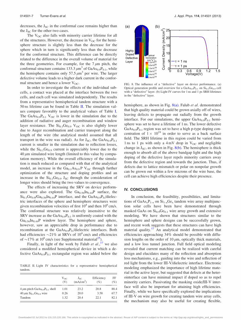
hemisphere, as shown in Fig. 8(a). Falub et al. demonstrated
that high quality material could be grown axially off of wires,
leaving defects to propagate out radially from the growth
interface. For our simulations, the upper GaAs0.9P0.1 hemi-
sphere was set to have a lifetime of 1 ns. The lower defective
GaAs0.9P0.1 region was set to have a high p-type doping con-
centration of 1� 1019 in order to serve as a back surface
field. The SRH lifetime in this region could be varied from
1 ns to 1 ps with only a 4 mV drop in VOC and negligible
change in JSC, as shown in Fig. 8(b). The hemisphere is thick
enough to absorb all of the above bandgap light and the high
doping of the defective layer repels minority carriers away
from the defective region and towards the junction. Thus, if
defects due to lattice mismatch or polar on nonpolar growth
can be grown out within a few microns of the wire base, the
cell can achieve high efficiencies despite their presence.
IV. CONCLUSIONS
In conclusion, the feasibility, possibilities, and limita-
tions of GaAsxP1-x on Si1-xGex tandem wire array multijunc-
tion solar cells have been have demonstrated through
masked GaAs on Si0.9Ge0.1 wire array growth and extensive
modeling. We have shown that structures similar to the
hemisphere and sphere designs can be successfully grown,
and recent work suggests that these structures can have high
material quality.17 An analytical model demonstrated that
efficiencies approaching 34% should be possible with diffu-
sion lengths on the order of 10 lm, optically thick materials,
and a low loss tunnel junction. Full field optical modeling
revealed that current matching can be realized with careful
design and elucidates many of the reflection and absorption
loss mechanisms, e.g., guiding into the wire and reflection of
red light from the lower III-V/dielectric interface. Electronic
modeling emphasized the importance of high lifetime mate-
rial in the active layer, but suggested that defects at the heter-
ointerface can have minimal impact if doped so as to repel
minority carriers. Passivating the masking oxide/III-V inter-
face will also be important for attaining high efficiencies.
Finally, while we have specifically explored the implications
of III-V on wire growth for creating tandem wire array cells,
the mechanism may also be useful for creating flexible,
TABLE II. Light IV characteristics for a representative hemispherical
tandem.
VOC
(V)
JSC
(mA/cm2)
Efficiency
(%)
FF
(%)
4 lm pitch GaAs0.9P0.1 shell 1.01 23.2 20.8 88.4
40 lm Si0.1Ge0.9 wire 0.26 20.0 3.58 67.7
Tandem 1.32 20.4 22.1 82.1
FIG. 8. The influence of a “defective” layer on device performance. (a)
Optical generation profile and overview for a GaAs0.9P0.1 on Si0.1Ge0.9 cell
with a “defective” layer. (b) Light IV curves for 1 ns and 1 ps SRH lifetimes
in the “defective” layer.
014501-7 Turner-Evans et al. J. Appl. Phys. 114, 014501 (2013)
Downloaded 02 Jul 2013 to 131.215.220.166. This article is copyrighted as indicated in the abstract. Reuse of AIP content is subject to the terms at: http://jap.aip.org/about/rights_and_permissions
standalone III–V cells, LEDs, or other devices on a reusable
Si wafer.
ACKNOWLEDGMENTS
We are grateful to Emily Warmann for assistance in
detailed balance calculations, to Dr. Mike Kelzenberg and
Dr. Mike Deceglie for their aid with Sentaurus, to Dr. Nick
Strandwitz for helpful discussion, and to all of our teachers
and family for their help and support through the years.
Support for this work was provided by the United States
Department of Energy under Grant No. DE-EE0005311.
D.B.T-E. acknowledges the NSF for fellowship support.
1E. Garnett and P. D. Yang, Nano Lett. 10, 1082 (2010).2M. D. Kelzenberg, S. W. Boettcher, J. A. Petykiewicz, D. B. Turner-
Evans, M. C. Putnam, E. L. Warren, J. M. Spurgeon, R. M. Briggs, N. S.
Lewis, and H. A. Atwater, Nature Mater. 9, 329 (2010).3M. D. Kelzenberg, D. B. Turner-Evans, M. C. Putnam, S. W. Boettcher,
R. M. Briggs, J. Y. Baek, N. S. Lewis, and H. A. Atwater, Energy
Environ. Sci. 4, 866 (2011).4M. C. Putnam, S. W. Boettcher, M. D. Kelzenberg, D. B. Turner-Evans,
J. M. Spurgeon, E. L. Warren, R. M. Briggs, N. S. Lewis, and H. A.
Atwater, Energy Environ. Sci. 3, 1037 (2010).5H. Goto, K. Nosaki, K. Tomioka, S. Hara, K. Hiruma, J. Motohisa, and T.
Fukui, Appl. Phys. Express 2, 035004 (2009).6G. Mariani, P.-S. Wong, A. M. Katzenmeyer, F. L�eonard, J. Shapiro, and
D. L. Huffaker, Nano Lett. 11, 2490 (2011).7K. Cho, D. J. Ruebusch, M. H. Lee, J. H. Moon, A. C. Ford, R. Kapadia,
K. Takei, O. Ergen, and A. Javey, Appl. Phys. Lett. 98, 203101 (2011).8Z. Fan, R. Kapadia, P. W. Leu, X. Zhang, Y.-L. Chueh, K. Takei, K. Yu,
A. Jamshidi, A. A. Rathore, D. J. Ruebusch, M. Wu, and A. Javey, Nano
Lett. 10, 3823 (2010).9L. Tsakalakos, J. Balch, J. Fronheiser, B. A. Korevaar, O. Sulima, and J.
Rand, Appl. Phys. Lett. 91, 233117 (2007).10C. E. Kendrick, H. P. Yoon, Y. A. Yuwen, G. D. Barber, H. Shen, T. E.
Mallouk, E. C. Dickey, T. S. Mayer, and J. M. Redwing, Appl. Phys. Lett.
97, 143108 (2010).11Z. Fan, H. Razavi, J.-W. Do, A. Moriwaki, O. Ergen, Y.-L. Chueh, P. W.
Leu, J. C. Ho, T. Takahashi, L. A. Reichertz, S. Neale, K. Yu, M. Wu,
J. W. Ager, and A. Javey, Nature Mater. 8, 648 (2009).
12J. Wallentin, N. Anttu, D. Asoli, M. Huffman, I. Aberg, M. H.
Magnusson, G. Siefer, P. Fuss-Kailuweit, F. Dimroth, B. Witzigmann,
H. Q. Xu, L. Samuelson, K. Deppert, and M. T. Borgstr€om, Science
339, 1057 (2013).13K. E. Plass, M. A. Filler, J. M. Spurgeon, B. M. Kayes, S. Maldonado,
B. S. Brunschwig, H. A. Atwater, and N. S. Lewis, Adv. Mater. 21, 325
(2009).14J. M. Spurgeon, K. E. Plass, B. M. Kayes, B. S. Brunschwig, H. A.
Atwater, and N. S. Lewis, Appl. Phys. Lett. 93, 032112 (2008).15S. W. Boettcher, J. M. Spurgeon, M. C. Putnam, E. L. Warren, D. B.
Turner-Evans, M. D. Kelzenberg, J. R. Maiolo, H. A. Atwater, and N. S.
Lewis, Science 327, 185 (2010).16N. C. Strandwitz, D. B. Turner-Evans, A. C. Tamboli, C. T. Chen, H. A.
Atwater, and N. S. Lewis, Adv. Energy Mater. 2, 1109 (2012).17C. V. Falub, H. von K€anel, F. Isa, R. Bergamaschini, A. Marzegalli, D.
Chrastina, G. Isella, E. M€uller, P. Niedermann, and L. Miglio, Science
335, 1330 (2012).18K. K. Lew, L. Pan, E. C. Dickey, and J. M. Redwing, Adv. Mater. 15,
2073 (2003).19E. I. Givargizov, J. Cryst. Growth 20, 217 (1973).20B. M. Kayes, M. A. Filler, M. C. Putnam, M. D. Kelzenberg, N. S. Lewis,
and H. A. Atwater, Appl. Phys. Lett. 91, 103110 (2007).21B. M. Kayes, H. A. Atwater, and N. S. Lewis, J. Appl. Phys. 97, 114302
(2005).22J. Humlicek, in Handbook of Optical Constants of Solids, edited by E. D.
Palik (Elsevier, 1998), Vol. III, Part II, Chap. 22.23The Ioffe Institute (Ioffe Institute, St. Petersburg, 2001), Vol. 2012, see
http://www.ioffe.rssi.ru/SVA/NSM/Semicond/.24C. F. Bohren and D. R. Huffman, Absorption and Scattering of Light by
Small Particles (John Wiley & Sons, New York, 2004).25See supplementary material at http://dx.doi.org/10.1063/1.4812397 for
more information and a plot comparing the Mie theory and Beer Lambert
absorption; further discussion of the effect of increasing the SRV; further
analysis of series resistance effects; further comparison of two dimensional
vs. three dimensional simulations; a comparison between the course and
fine simulations; a summary of the optical absorption and loss mechanisms
and further discussion of the pitch dependence; and more information of
the specific parameters.26R. L.-Y. Sah, R. N. Noyce, and W. Shockley, Proc. IRE 45, 1228 (1957).27M. T. Sheldon, C. N. Eisler, and H. A. Atwater, Adv. Energy Mater. 2,
339 (2012).28See http://www.lumerical.com for more information on the software.29V. E. Ferry, L. A. Sweatlock, D. Pacifici, and H. A. Atwater, Nano Lett. 8,
4391 (2008).30See http://www.synopsys.com for more information on the software.
014501-8 Turner-Evans et al. J. Appl. Phys. 114, 014501 (2013)
Downloaded 02 Jul 2013 to 131.215.220.166. This article is copyrighted as indicated in the abstract. Reuse of AIP content is subject to the terms at: http://jap.aip.org/about/rights_and_permissions